WO2010070964A1 - 回路モジュール及びその管理方法 - Google Patents
回路モジュール及びその管理方法 Download PDFInfo
- Publication number
- WO2010070964A1 WO2010070964A1 PCT/JP2009/066907 JP2009066907W WO2010070964A1 WO 2010070964 A1 WO2010070964 A1 WO 2010070964A1 JP 2009066907 W JP2009066907 W JP 2009066907W WO 2010070964 A1 WO2010070964 A1 WO 2010070964A1
- Authority
- WO
- WIPO (PCT)
- Prior art keywords
- substrate
- circuit module
- identification code
- module
- circuit
- Prior art date
- Legal status (The legal status is an assumption and is not a legal conclusion. Google has not performed a legal analysis and makes no representation as to the accuracy of the status listed.)
- Ceased
Links
Images






Classifications
-
- H—ELECTRICITY
- H05—ELECTRIC TECHNIQUES NOT OTHERWISE PROVIDED FOR
- H05K—PRINTED CIRCUITS; CASINGS OR CONSTRUCTIONAL DETAILS OF ELECTRIC APPARATUS; MANUFACTURE OF ASSEMBLAGES OF ELECTRICAL COMPONENTS
- H05K1/00—Printed circuits
- H05K1/02—Details
- H05K1/0266—Marks, test patterns or identification means
-
- H—ELECTRICITY
- H05—ELECTRIC TECHNIQUES NOT OTHERWISE PROVIDED FOR
- H05K—PRINTED CIRCUITS; CASINGS OR CONSTRUCTIONAL DETAILS OF ELECTRIC APPARATUS; MANUFACTURE OF ASSEMBLAGES OF ELECTRICAL COMPONENTS
- H05K2201/00—Indexing scheme relating to printed circuits covered by H05K1/00
- H05K2201/09—Shape and layout
- H05K2201/09818—Shape or layout details not covered by a single group of H05K2201/09009 - H05K2201/09809
- H05K2201/09927—Machine readable code, e.g. bar code
-
- Y—GENERAL TAGGING OF NEW TECHNOLOGICAL DEVELOPMENTS; GENERAL TAGGING OF CROSS-SECTIONAL TECHNOLOGIES SPANNING OVER SEVERAL SECTIONS OF THE IPC; TECHNICAL SUBJECTS COVERED BY FORMER USPC CROSS-REFERENCE ART COLLECTIONS [XRACs] AND DIGESTS
- Y10—TECHNICAL SUBJECTS COVERED BY FORMER USPC
- Y10T—TECHNICAL SUBJECTS COVERED BY FORMER US CLASSIFICATION
- Y10T29/00—Metal working
- Y10T29/49—Method of mechanical manufacture
- Y10T29/49002—Electrical device making
- Y10T29/49108—Electric battery cell making
-
- Y—GENERAL TAGGING OF NEW TECHNOLOGICAL DEVELOPMENTS; GENERAL TAGGING OF CROSS-SECTIONAL TECHNOLOGIES SPANNING OVER SEVERAL SECTIONS OF THE IPC; TECHNICAL SUBJECTS COVERED BY FORMER USPC CROSS-REFERENCE ART COLLECTIONS [XRACs] AND DIGESTS
- Y10—TECHNICAL SUBJECTS COVERED BY FORMER USPC
- Y10T—TECHNICAL SUBJECTS COVERED BY FORMER US CLASSIFICATION
- Y10T29/00—Metal working
- Y10T29/49—Method of mechanical manufacture
- Y10T29/49002—Electrical device making
- Y10T29/49108—Electric battery cell making
- Y10T29/49115—Electric battery cell making including coating or impregnating
-
- Y—GENERAL TAGGING OF NEW TECHNOLOGICAL DEVELOPMENTS; GENERAL TAGGING OF CROSS-SECTIONAL TECHNOLOGIES SPANNING OVER SEVERAL SECTIONS OF THE IPC; TECHNICAL SUBJECTS COVERED BY FORMER USPC CROSS-REFERENCE ART COLLECTIONS [XRACs] AND DIGESTS
- Y10—TECHNICAL SUBJECTS COVERED BY FORMER USPC
- Y10T—TECHNICAL SUBJECTS COVERED BY FORMER US CLASSIFICATION
- Y10T29/00—Metal working
- Y10T29/49—Method of mechanical manufacture
- Y10T29/49002—Electrical device making
- Y10T29/49117—Conductor or circuit manufacturing
- Y10T29/49121—Beam lead frame or beam lead device
-
- Y—GENERAL TAGGING OF NEW TECHNOLOGICAL DEVELOPMENTS; GENERAL TAGGING OF CROSS-SECTIONAL TECHNOLOGIES SPANNING OVER SEVERAL SECTIONS OF THE IPC; TECHNICAL SUBJECTS COVERED BY FORMER USPC CROSS-REFERENCE ART COLLECTIONS [XRACs] AND DIGESTS
- Y10—TECHNICAL SUBJECTS COVERED BY FORMER USPC
- Y10T—TECHNICAL SUBJECTS COVERED BY FORMER US CLASSIFICATION
- Y10T29/00—Metal working
- Y10T29/49—Method of mechanical manufacture
- Y10T29/49002—Electrical device making
- Y10T29/49117—Conductor or circuit manufacturing
- Y10T29/49124—On flat or curved insulated base, e.g., printed circuit, etc.
- Y10T29/49155—Manufacturing circuit on or in base
Definitions
- the present invention relates to a circuit module and a management method thereof, and more particularly, to a circuit module having an identification code and a management method thereof.
- Patent Document 1 is disclosed as a method for performing production history management of such circuit modules and aggregate substrates.
- a multi-sided board 10 shown in FIG. 1 is a board in which divided boards 11 to 14 divided into, for example, four pieces after component mounting are arranged in a matrix, and a board identification code (board ID) is placed on a portion other than the divided board. 20 and a circuit identification code (circuit ID) 22 are attached to each of the divided substrates 11 to 14.
- the board identification code 20 is unique so as not to overlap with other multi-sided boards 10, and the circuit identification code 22 includes the board identification code 20 as a part thereof.
- the circuit identification codes 22 of the divided boards 11 to 14 are [00010-001] [00010-002] [00010-003] [00010-004], respectively. Can do.
- the circuit module identification code is temporarily assigned to the resin-sealed interior.
- the identification code cannot be easily read during failure analysis.
- an object of the present invention is to provide a small circuit module to which an identification code is attached and a management method thereof.
- the circuit module of the present invention is configured as follows. (1) A circuit module obtained by dividing an aggregate substrate on which a plurality of circuit modules are formed, A rectangular plate-shaped module substrate; An electrode formed on the first main surface of the module substrate; A resist film formed on the first main surface of the module substrate, On the first main surface of the module substrate, there is provided a direction identification region indicating the direction of the module substrate by partial formation / non-formation of the electrode or partial formation / non-formation of the resist film. Have It is assumed that a first identification code having position information of the circuit module on the collective substrate is formed in the direction identification area.
- the first identification code is represented by a dot pattern. As a result, the required resolution is lower than when characters are formed, and an identification code can be formed in a limited space.
- the first identification code is constituted by partial formation / non-formation of the electrode or partial formation / non-formation of the resist film.
- the first identification code can be formed simultaneously when forming the electrode pattern, or the first identification code can be formed simultaneously when forming the resist film, and a special process for forming the first identification code Is no longer necessary.
- the first identification code is constituted by partial formation / non-formation of the electrode, and the direction identification region is covered with the resist film. With this configuration, the first identification code is difficult to peel off, and erroneous recognition is unlikely to occur when the direction identification region is recognized by light reflection.
- the first main surface of the module substrate is a mounting surface of the circuit module, A plurality of components are arranged on the second main surface of the module substrate, The plurality of components are sealed with resin on the module substrate. Thereby, a metal cap becomes unnecessary and it can reduce in thickness. In addition, the identification code can be easily read with the resin sealed. That is, the structure is particularly suitable for a resin-sealed circuit module.
- a second identification code is formed on the outer surface of the module substrate on the second main surface side.
- the second identification code has identification information of the collective board.
- the collective board can be identified by the second identification code, and the position in the collective board can be identified by the first identification code.
- the second identification code is different for each manufacture, but the first identification code can always be formed in the same pattern.
- the first identification code having a fixed pattern can be basically formed by a printing method, there is no increase in cost for forming the first identification code.
- the fluctuating identification code is provided as the second identification code, the number of digits of the second identification code can be minimized, and the circuit module 1 can be formed when forming by laser marking or the like. The time required for each piece does not increase.
- the circuit module management method of the present invention is configured as follows. (8) forming a plurality of circuit modules on the assembly board; Forming a first identification code having position information of a circuit module on the collective substrate in a direction recognition area in each module substrate portion of the collective substrate; Dividing the collective substrate into the module substrate portions; Reading the first identification code to obtain position information of the circuit module on the collective substrate; To manage the circuit module.
- the circuit module can be reduced in size. Further, it is possible to manage from which position in the collective substrate the circuit module is divided, and for example, defect analysis and traceability are improved.
- FIG. 3 is a diagram showing a configuration of a first identification code representing a position on a collective substrate 100 of a module substrate 30 formed in a direction identifying region 39. It is a figure showing the relationship between the pattern of a 1st identification code, and information.
- FIG. 6A is a plan view of the circuit module 50.
- 6B shows the display of the second identification code 51 and its contents. It is a top view by the side of the mounting surface of two types of circuit modules which concern on 2nd Embodiment. It is a figure which shows the structure of the 1st identification code used with the circuit module which concerns on 3rd Embodiment. It is a figure showing the relationship between the pattern of the 1st identification code shown in FIG. 8, and information. It is a top view by the side of the board
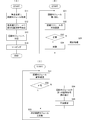
- FIG. 14A is a flowchart showing a procedure of a circuit module manufacturing method
- FIG. 14B is a flowchart showing a procedure for mounting the circuit module
- FIG. 14C is a diagram showing operation confirmation and failure analysis of the circuit module. It is a flowchart which shows a procedure.
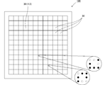
- FIG. 2 is a plan view of the collective substrate in the process of manufacturing the circuit module according to the first embodiment.
- the collective substrate 100 includes a plurality of module substrate units 30. In this example, a module substrate portion of 12 rows ⁇ 12 columns is provided, and 144 circuit modules are obtained by dividing the collective substrate 100 later.
- FIG. 3 is a plan view showing the configuration of one module substrate 30, and is a plan view on the mounting surface side (first main surface side) when completed as a circuit module.
- Signal input / output terminals 42 are arranged on the periphery (four sides) of the module substrate 30.
- Outer ground terminals 41 are formed at the four corners of the module substrate 30.
- Signal input / output terminals may be formed at all or some of the four corners of the module substrate 30. The same applies to other embodiments described later.
- the inner side of the module substrate 30 surrounded by the signal input / output terminal 42 and the outer ground terminal 41 is an inner ground terminal forming region 31.
- an inner ground terminal formation region 31 a plurality of inner ground terminals 40 arranged in a vertical and horizontal matrix are formed.
- the terminal formed in the inner region surrounded by the signal input / output terminal 42 and the outer ground terminal 41 is not limited to the ground terminal, and may be another terminal or electrode.
- a signal input terminal may be formed.
- 6 rows ⁇ 6 columns of inner ground terminals 40 are formed in the inner ground terminal forming region 31, but one corner is a direction identifying region 39, and the direction identifying region 39 has an inner side.
- the ground terminal 40 is not formed.
- a first identification code having position information of the module substrate 30 is formed in the direction identification area 39.
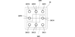
- FIG. 4 is a diagram showing a configuration of a first identification code representing the position of the module substrate 30 formed in the direction identification region 39 on the collective substrate 100.
- the line position information 38R is constituted by the four dot formation regions 38R1, 38R2, 38R3, 38R4.
- the row position information 38C is constituted by the four dot formation regions 38C1, 38C2, 38C3, 38C4.
- the row position information is given by the 4-bit binary code by the four dots in the dot formation areas 38R1 to 38R4, and the column position information is given by the 4-bit binary code by the four dots 38C1 to 38C4.
- the dots are formed by electrodes.
- the bit of (row, column) is represented as (0011, 0100). You can see that they are eyes. That is, it can be seen that this is the module substrate in the module substrate region 30 (4, 3) shown in FIG.
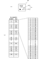
- FIG. 5 is a diagram illustrating the relationship between the pattern of the first identification code and the information.
- row position information and column position information are represented simultaneously.
- “row / column” is a value that represents the number of rows and the number of columns by a decimal code.
- the “bit representation” is a 4-bit binary code.
- the “corresponding mark” is a pattern of the row position information 38R and the column position information 38C shown in FIG. In this way, the maximum (16 rows, 16 columns) module board positions are represented.
- the manufacturing process of the circuit module based on the collective substrate shown in FIG. 2 is as follows. (1) A predetermined electronic component is mounted on the component mounting surface of the collective substrate 100 shown in FIG. 2 (the surface on the back side from the direction shown in FIG. 2). (2) The entire component mounting surface of the collective substrate 100 is sealed with an insulating resin. (3) A groove having a depth from the resin sealing surface side to the center of the thickness of the collective substrate 100 is formed at the boundary line of each module substrate 30. (4) A conductive paste is applied to the surface of the sealed resin and dried and cured.
- FIG. 6A is a plan view of the circuit module 50 manufactured by the manufacturing process.
- FIG. 6B is a diagram showing the display of the second identification code 51A and its contents.
- the second identification code 51 based on the collective substrate number 51A and the production number 51B is laser-marked. It is formed with.
- the production number 51B represents a production lot
- the collective board number 51A represents the number of collective boards in the production factory and production time.
- the second identification code represents the board number of the collective board with two digits of alphanumeric characters 0 to 9 and A to Z.
- the notation of the second identification code 51 is 2B, it means that the circuit module 50 is separated from the 76th assembly board.
- the direction identification region 39 may be entirely covered with a resist film (that is, so as to cover the dot-shaped electrode which is the first identification code 38).
- the resin sealing is performed.
- the present invention can also be applied to the case of sealing with a metal case (cap) without sealing with resin. The same applies to other embodiments described later.
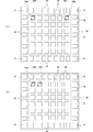
- FIGS. 7A and 7B are plan views on the mounting surface side of two types of circuit modules according to the second embodiment.
- two direction identification regions 39A and 39B are provided in the inner ground terminal formation region 31.
- Row position information 38R is formed in the direction identification area 39A.
- Column position information 38C is formed in the direction identification area 39B.
- the first identification code may be formed using a plurality of regions of the inner ground terminal 40.
- FIG. 8 is a diagram illustrating a configuration of a first identification code used in the circuit module according to the third embodiment.
- the first identification code includes row position information 37R and column position information 37C.
- the number in the circle is the bit digit number.
- the direction identification area 39 may be provided with 8-bit row position information and 8-bit column position information.
- FIG. 9 is a diagram showing the relationship between the pattern of the first identification code shown in FIG. 8 and information.
- row position information and column position information are represented simultaneously.
- “row / column” is a value representing what row and which column is represented by a decimal code.
- the “bit representation” is an 8-bit binary code.
- the “corresponding mark” is a pattern of the row position information 38R or the column position information 38C shown in FIG. In this way, the maximum (255 rows, 255 columns) of module board position information can be provided.
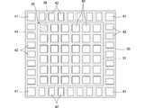
- FIG. 10 is a plan view on the board mounting surface side of the circuit module according to the fourth embodiment, and is a plan view on the mounting surface side (first main surface side) when the circuit module is completed.
- Signal input / output terminals 42 are arranged on the periphery (four sides) of the module substrate 30.
- Outer ground terminals 41 are formed at the four corners of the module substrate 30.
- An inner side of the module substrate 30 surrounded by the signal input / output terminal 42 and the outer ground terminal 41 is an inner ground terminal forming region 31.
- a plurality of inner ground terminals 40 are individually formed in the inner ground terminal forming region 31.
- a resist film 43 is formed between these electrodes.
- the inner ground terminal 40 is not formed, and the first identification code 38 is configured by the electrode of the dot pattern.
- This direction identification region 39 is entirely covered with a resist film 43, including the surface of the first identification code 38 by the electrode of the dot pattern. This can prevent each electrode from being peeled off, and has the effect of preventing erroneous recognition when recognizing the position of the direction identification region based on the difference in the amount of reflected light.
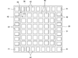
- FIG. 11 is a plan view of the circuit module mounting surface side of the circuit module according to the fifth embodiment, and is a plan view of the mounting surface side (first main surface side) when the circuit module is completed.
- Signal input / output terminals 42 are arranged on the periphery (four sides) of the module substrate 30.
- Outer ground terminals 41 are formed at the four corners of the module substrate 30.
- the inner side of the module substrate 30 surrounded by the signal input / output terminal 42 and the outer ground terminal 41 is an inner ground terminal forming region 31.
- a continuous ground electrode is formed in the inner ground terminal forming region 31.
- a first identification code 38 is formed in the direction identification region 39 by a partial opening (extraction pattern) of the ground electrode.
- the inner ground terminal 40 is provided in a region other than the direction identification region 39 in the inner ground terminal formation region 31 by a partial opening of the resist film 43.
- Resist films 43 are also formed between the adjacent signal input / output terminals 42 and between the outer ground terminal 41 and the signal input / output terminal 42.
- the direction identifying region 39 is entirely covered with a resist film 43, including the surface of the first identification code 38 due to the pattern of the ground electrode. This can prevent each electrode from being peeled off, and has the effect of preventing erroneous recognition when recognizing the position of the direction identification region based on the difference in the amount of reflected light.
- FIG. 12 is a plan view of the circuit module mounting surface side according to the sixth embodiment, and is a plan view of the mounting surface side (first main surface side) when the circuit module is completed.
- Signal input / output terminals 42 are arranged on the periphery (four sides) of the module substrate 30.
- Outer ground terminals 41 are formed at the four corners of the module substrate 30.
- the inner side of the module substrate 30 surrounded by the signal input / output terminal 42 and the outer ground terminal 41 is an inner ground terminal forming region 31.
- a continuous ground electrode is formed in the inner ground terminal forming region 31.
- An inner ground terminal 40 is formed in the inner ground terminal formation region 31 by openings of a plurality of resist films 43.
- a first identification code 38 is formed in the direction identification region 39 by a partial opening (extraction pattern) of the resist film.
- the first identification code may be formed by the pattern of the resist film. With this configuration, the first identification code 38 is difficult to peel off.
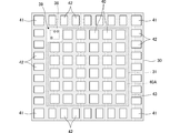
- FIG. 13 is a plan view of the mounting surface side of the circuit module according to the seventh embodiment.
- the continuous ground electrode 40A is formed in the inner ground terminal formation region 31, the inner ground terminal 40 is provided by the opening of the resist film 43, and the first identification code 38 is formed by the pattern of the resist film. ing.
- the ground electrode is not formed around the first identification code 38 (direction identification region 39), and the first identification code 38 is formed only by a resist film in this portion.
- the dot pattern is not limited to a round shape, and may be a rectangle.
- more positions can be expressed with a smaller number of dots. For example, it is possible to give position information in a range exceeding 16 rows ⁇ 16 columns with eight dots shown in FIG. 5 and to identify the position information.
- the shape of the dot pattern of the first identification code may be varied according to the difference.
- These dot patterns can have various shapes such as a round shape, a rectangle shape, a triangle shape, a cross shape, and a hexagon shape.
- the first identification code is not limited to a dot pattern, and may be a bar shape. Further, not only binary codes but also one-dimensional or two-dimensional barcodes may be used. Furthermore, although the first identification code may be formed of characters, the formation of the first identification code using dots or bars has the effect that it can be formed in a limited space.
- FIG. 14A is a flowchart showing the procedure of the circuit module manufacturing method.
- a plurality of circuit modules are formed on the collective substrate 100 (S11).
- a second identification code is formed on the surface side of each circuit module by the laser marking method (S12).
- the circuit module is divided into a plurality of circuit modules and taped so as to fit a predetermined parts feeder (S13 ⁇ S14).
- FIG. 14B is a flowchart showing the mounting procedure of the circuit module.
- the circuit module is taken out from the tape feeder, and the direction of the circuit module is recognized from the position of the direction identification area (S21 ⁇ S22). This is performed by recognizing an image by imaging the mounting surface side of the circuit module with a camera while the circuit module is sucked by a vacuum chuck. If normal, the circuit module is mounted on the mounting board (S23 ⁇ S24). If the direction is abnormal, an abnormal process such as rejecting the circuit module is performed (S25). The circuit module is mounted by repeating the above processing.
- FIG. 14C is a flowchart showing a procedure for operation confirmation and failure analysis of the circuit module.
- the circuit module is connected to the operation check device, and the operation check is automatically performed (S31). If normal, replace with the next circuit module and repeat the same process (S32 ⁇ S33 ⁇ S31). If it is abnormal, the first identification code on the mounting surface side of the circuit module is read, and the position from which the circuit module is cut out is grasped. Then, the failure analysis of the circuit module is performed (S34 ⁇ S35). This makes it possible to statistically manage the relationship (distribution, etc.) between the position of the collective substrate and the failure rate or failure mode.
- the identification code can be read by image recognition, or by using a laser or a microscope.
Landscapes
- Engineering & Computer Science (AREA)
- Microelectronics & Electronic Packaging (AREA)
- Structure Of Printed Boards (AREA)
Abstract
Description
このような回路モジュール及び集合基板の生産履歴管理を行う方法として特許文献1が開示されている。
(1)複数の回路モジュールが形成された集合基板の分割によって得られる回路モジュールであって、
矩形板状のモジュール基板と、
前記モジュール基板の第1の主面に形成された電極と、
前記モジュール基板の第1の主面に形成されたレジスト膜と、を備え、
前記モジュール基板の第1の主面には、前記電極の部分的な形成/非形成によって、または前記レジスト膜の部分的な形成/非形成によって、前記モジュール基板の方向を表す方向識別用領域を有し、
前記方向識別用領域に前記集合基板上の回路モジュールの位置情報をもつ第1の識別符号が形成されたものとする。
これにより、文字を形成する場合よりも必要解像度は低くてすみ、限られたスペースに識別符号を形成できる。
この構成により、電極パターンの形成時に前記第1の識別符号を同時に形成でき、またはレジスト膜の形成時に前記第1の識別符号を同時に形成でき、第1の識別符号を形成するための特別な工程が不要となる。
この構成により、第1の識別符号が剥がれにくく、前記方向識別用領域を光反射により認識する際に誤認識が生じにくい。
前記モジュール基板の第2の主面に複数の部品が配置され、
前記複数の部品は前記モジュール基板上で樹脂により封止されているものとする。
これにより、金属キャップが不要となり、薄型化できる。しかも、樹脂封止された状態のまま識別符号を容易に読み取ることができる。すなわち、特に樹脂封止された回路モジュールに適した構造となる。
この構成により、2つの識別符号を用いて回路モジュールの識別機能が高まる。
これにより、第2の識別符号で集合基板が識別でき、第1の識別符号で集合基板内での位置が識別できる。また、第2の識別符号は製造毎に異なるが、第1の識別符号は常に同じパターンに形成できる。このように一定パターンの第1の識別符号は基本的に印刷法で形成できるので、第1の識別符号を形成するためのコストの増加がない。しかも、変動する識別符号のみ第2の識別符号として設けるだけであるので、第2の識別符号の桁数などを最小限なものとすることができ、レーザマーキング等で形成する際に回路モジュール1個あたりに要する時間が長くなることがない。
(8) 集合基板に複数の回路モジュールを形成するステップと、
前記集合基板の各モジュール基板部内の方向認識用領域に、前記集合基板上の回路モジュールの位置情報をもつ第1の識別符号を形成するステップと、
前記集合基板を前記各モジュール基板部に分割するステップと、
前記第1の識別符号を読み取り、前記集合基板上の回路モジュールの位置情報を取得するステップと、
によって回路モジュールを管理する。
第1の実施形態に係る回路モジュールについて図2~図6を参照して説明する。
図2は第1の実施形態に係る回路モジュールの製造途中における集合基板の状態での平面図である。集合基板100には複数のモジュール基板部30が備えられている。この例では12行×12列のモジュール基板部を備え、後にこの集合基板100を分割することによって144個の回路モジュールを得ることになる。
なお、モジュール基板30の四隅のすべてまたは幾つかに信号入出力端子を形成してもよい。このことは、後に示す他の実施形態についても同様である。
このようにして、最大(16行,16列)のモジュール基板の位置を表す。
(1)図2に示した集合基板100の部品搭載面(図2に示された方向からは裏面側になる面)に所定の電子部品を搭載する。
(2)集合基板100の部品搭載面の全体を絶縁性の樹脂によって封止する。
(3)各モジュール基板30の境界線で、樹脂封止面側から集合基板100の厚みの中央までの深さの溝を形成する。
(4)封止された前記樹脂の表面に導電性ペーストを塗布し、乾燥硬化させる。
(5)その後、各回路モジュールの天面(実装面とは反対側の面)となる位置に、集合基板の識別(その回路モジュールがどの集合基板から分割されたものであるかを表す識別情報)をもつ第2の識別符号を付与する。
(6)最後に、集合基板100全体をカットすることによって個別の回路モジュールを構成する。
図7(A)、図7(B)は、第2の実施形態に係る2種類の回路モジュールの実装面側の平面図である。
図8は、第3の実施形態に係る回路モジュールで用いる第1の識別符号の構成を示す図である。この第1の識別符号は、行位置情報37R及び列位置情報37Cを備えている。丸内の数字はビットの桁番号である。
方向識別用領域39に対してこのように8ビットの行位置情報と8ビットの列位置情報とをもたせてもよい。
このようにして、最大(255行,255列)のモジュール基板の位置情報をもたせることができる。
図10は、第4の実施形態に係る回路モジュールの基板実装面側の平面図であり、回路モジュールとして完成したときの実装面側(第1の主面側)の平面図である。モジュール基板30の周辺部(四辺)には信号入出力端子42が配列されている。またモジュール基板30の四隅には外側グランド端子41が形成されている。
モジュール基板30の前記信号入出力端子42及び外側グランド端子41で囲まれた内側は内側グランド端子形成領域31である。この内側グランド端子形成領域31内に複数の内側グランド端子40が個別に形成されている。これらの各電極間にはレジスト膜43が形成されている。
このことによって、各電極の剥がれを防止できるとともに、方向識別用領域の位置をその光の反射量の違いにより認識する際に、誤認識が生じにくいという効果を奏する。
図11は、第5の実施形態に係る回路モジュールの基板実装面側の平面図であり、回路モジュールとして完成したときの実装面側(第1の主面側)の平面図である。モジュール基板30の周辺部(四辺)には信号入出力端子42が配列されている。またモジュール基板30の四隅には外側グランド端子41が形成されている。
モジュール基板30の、信号入出力端子42及び外側グランド端子41で囲まれた内側は内側グランド端子形成領域31である。この内側グランド端子形成領域31内に連続したグランド電極が形成されている。但し、方向識別用領域39にグランド電極の部分的な開口(抜きパターン)によって第1の識別符号38が形成されている。
このことによって、各電極の剥がれを防止できるとともに、方向識別用領域の位置をその光の反射量の違いにより認識する際に、誤認識が生じにくいという効果を奏する。
図12は、第6の実施形態に係る回路モジュールの基板実装面側の平面図であり、回路モジュールとして完成したときの実装面側(第1の主面側)の平面図である。モジュール基板30の周辺部(四辺)には信号入出力端子42が配列されている。またモジュール基板30の四隅には外側グランド端子41が形成されている。
モジュール基板30の、信号入出力端子42及び外側グランド端子41で囲まれた内側は内側グランド端子形成領域31である。この内側グランド端子形成領域31内に連続したグランド電極が形成されている。そして、内側グランド端子形成領域31内に複数のレジスト膜43の開口による内側グランド端子40が形成されている。但し、方向識別用領域39にはレジスト膜の部分的な開口(抜きパターン)によって第1の識別符号38が形成されている。
この構成により、第1の識別符号38が剥がれにくくなる。
図13は、第7の実施形態に係る回路モジュールの実装面側の平面図である。この例では、内側グランド端子形成領域31に、連続したグランド電極40Aが形成され、レジスト膜43の開口による内側グランド端子40が設けられるとともに、レジスト膜のパターンによって第1の識別符号38が形成されている。この第1の識別符号38の周囲(方向識別用領域39)にはグランド電極が形成されていなくて、この部分にレジスト膜のみによって第1の識別符号38が形成されている。
次に、この発明の回路モジュールの管理方法について図14のフローチャートを参照して説明する。
図14(A)は回路モジュールの製造方法の手順を示すフローチャートである。まず、第1の実施形態で図2等に示したように、集合基板100に対して複数の回路モジュールを形成する(S11)。続いて各回路モジュールの表面側に第2の識別符号をレーザマーキング法で形成する(S12)。その後、複数の回路モジュールへ分割し、所定のパーツフィーダに適合するようにテーピングする(S13→S14)。
もし異常であれば、その回路モジュールの実装面側の第1の識別符号を読み取り、その回路モジュールが集合基板のどの位置から切り出されたものであるかを把握する。そして、その回路モジュールの不良解析を行う(S34→S35)。このことにより、集合基板の位置と不良率や不良モードとの関係(分布等)を統計的に管理できる。
これにより、いつ製造されたどの集合基板のどこから分割された回路モジュールであるかを管理対象にでき、トレーサビリティが向上する。なお、識別符号の読み取りは、画像認識で行ったり、レーザー、顕微鏡を用いて行ったりできる。
30…モジュール基板,モジュール基板部
31…内側グランド端子形成領域
37C…列位置情報
37R…行位置情報
38…第1の識別符号
38C…列位置情報
38C1,38C2,38C3,38C4…ドット形成領域
38R…行位置情報
38R1,38R2,38R3,38R4…ドット形成領域
39…方向識別用領域
39A,39B…方向識別用領域
40…内側グランド端子
41…外側グランド端子
42…信号入出力端子
43…レジスト膜
50…回路モジュール
51…第2の識別符号
51A…集合基板番号
51B…製造番号
Claims (8)
- 複数の回路モジュールが形成された集合基板の分割によって得られる回路モジュールであって、
矩形板状のモジュール基板と、
前記モジュール基板の第1の主面に形成された電極と、
前記モジュール基板の第1の主面に形成されたレジスト膜と、を備え、
前記モジュール基板の第1の主面には、前記電極の部分的な形成/非形成によって、または前記レジスト膜の部分的な形成/非形成によって、前記モジュール基板の方向を表す方向識別用領域を有し、
前記方向識別用領域に前記集合基板上の前記モジュール基板の位置情報をもつ第1の識別符号が形成された回路モジュール。 - 前記第1の識別符号はドットパターンで表された、請求項1に記載の回路モジュール。
- 前記第1の識別符号は、前記電極の部分的な形成/非形成によって、または前記レジスト膜の部分的な形成/非形成によって構成された、請求項1または2に記載の回路モジュール。
- 前記第1の識別符号は、前記電極の部分的な形成/非形成によって構成され、且つ前記方向識別用領域が前記レジスト膜で覆われた、請求項1~3のいずれかに記載の回路モジュール。
- 前記モジュール基板の第1の主面は前記回路モジュールの実装面であり、
前記モジュール基板の第2の主面に複数の部品が配置され、
前記複数の部品は前記モジュール基板上で樹脂により封止されている、請求項1~4のいずれかに記載の回路モジュール。 - 前記モジュール基板の第2の主面側の外面に第2の識別符号が形成された、請求項1~5のいずれかに記載の回路モジュール。
- 前記第2の識別符号は、前記集合基板の識別情報をもつ、請求項6に記載の回路モジュール。
- 集合基板に複数の回路モジュールを形成するステップと、
前記集合基板の各モジュール基板部内の方向認識用領域に、前記集合基板上の回路モジュールの位置情報をもつ第1の識別符号を形成するステップと、
前記集合基板を前記各モジュール基板部に分割するステップと、
前記第1の識別符号を読み取り、前記集合基板上の回路モジュールの位置情報を取得するステップと、
を実行する回路モジュールの管理方法。
Priority Applications (3)
| Application Number | Priority Date | Filing Date | Title |
|---|---|---|---|
| CN200980150341.4A CN102246605B (zh) | 2008-12-16 | 2009-09-29 | 电路模块 |
| JP2010542907A JP5126370B2 (ja) | 2008-12-16 | 2009-09-29 | 回路モジュール |
| US13/155,463 US8431827B2 (en) | 2008-12-16 | 2011-06-08 | Circuit modules and method of managing the same |
Applications Claiming Priority (2)
| Application Number | Priority Date | Filing Date | Title |
|---|---|---|---|
| JP2008319852 | 2008-12-16 | ||
| JP2008-319852 | 2008-12-16 |
Related Child Applications (1)
| Application Number | Title | Priority Date | Filing Date |
|---|---|---|---|
| US13/155,463 Continuation US8431827B2 (en) | 2008-12-16 | 2011-06-08 | Circuit modules and method of managing the same |
Publications (1)
| Publication Number | Publication Date |
|---|---|
| WO2010070964A1 true WO2010070964A1 (ja) | 2010-06-24 |
Family
ID=42268639
Family Applications (1)
| Application Number | Title | Priority Date | Filing Date |
|---|---|---|---|
| PCT/JP2009/066907 Ceased WO2010070964A1 (ja) | 2008-12-16 | 2009-09-29 | 回路モジュール及びその管理方法 |
Country Status (4)
| Country | Link |
|---|---|
| US (1) | US8431827B2 (ja) |
| JP (1) | JP5126370B2 (ja) |
| CN (1) | CN102246605B (ja) |
| WO (1) | WO2010070964A1 (ja) |
Cited By (3)
| Publication number | Priority date | Publication date | Assignee | Title |
|---|---|---|---|---|
| JP2013125935A (ja) * | 2011-12-16 | 2013-06-24 | Murata Mfg Co Ltd | 基板集合体 |
| JP2014116383A (ja) * | 2012-12-07 | 2014-06-26 | Murata Mfg Co Ltd | 電子部品 |
| JP2017118149A (ja) * | 2017-03-21 | 2017-06-29 | 株式会社村田製作所 | 電子部品の実装構造 |
Families Citing this family (6)
| Publication number | Priority date | Publication date | Assignee | Title |
|---|---|---|---|---|
| TWM468814U (zh) * | 2013-08-28 | 2013-12-21 | Bellwether Electronic Corp | 連接器料帶及其連接器模組 |
| JP6622121B2 (ja) * | 2016-03-16 | 2019-12-18 | 新光電気工業株式会社 | 配線基板及びその検査方法 |
| CN107708288A (zh) * | 2017-09-08 | 2018-02-16 | 江西景旺精密电路有限公司 | 一种pcb板及其加工方法 |
| JP6740268B2 (ja) * | 2018-02-23 | 2020-08-12 | 株式会社三共 | 遊技機 |
| CN117813917A (zh) * | 2021-07-26 | 2024-04-02 | 电化株式会社 | 接合基板、电路基板及其制造方法、以及单片基板及其制造方法 |
| KR20240011486A (ko) * | 2022-07-19 | 2024-01-26 | 삼성전자주식회사 | 기판 |
Citations (9)
| Publication number | Priority date | Publication date | Assignee | Title |
|---|---|---|---|---|
| JPH0338654U (ja) * | 1989-08-24 | 1991-04-15 | ||
| JPH05218600A (ja) * | 1992-02-04 | 1993-08-27 | Ibiden Co Ltd | プリント配線板 |
| JP2001156217A (ja) * | 1999-11-29 | 2001-06-08 | Hitachi Ltd | 半導体装置の製造方法 |
| JP2002043703A (ja) * | 2000-07-31 | 2002-02-08 | Optrex Corp | 多面取りマザー基板および液晶表示素子 |
| JP2003188039A (ja) * | 2001-12-20 | 2003-07-04 | Murata Mfg Co Ltd | 積層型電子部品 |
| JP2005183939A (ja) * | 2003-11-28 | 2005-07-07 | Matsushita Electric Ind Co Ltd | 回路基板の生産方法とシステム |
| JP2005277075A (ja) * | 2004-03-24 | 2005-10-06 | Kyocera Corp | 配線基板 |
| JP2005294635A (ja) * | 2004-04-01 | 2005-10-20 | Seiko Epson Corp | 配線基板および電子部品モジュール |
| JP2007042934A (ja) * | 2005-08-04 | 2007-02-15 | Juki Corp | 多面取り基板の生産履歴管理方法及び多面取り基板 |
Family Cites Families (64)
| Publication number | Priority date | Publication date | Assignee | Title |
|---|---|---|---|---|
| US5032542A (en) * | 1988-11-18 | 1991-07-16 | Sanyo Electric Co., Ltd. | Method of mass-producing integrated circuit devices using strip lead frame |
| US5171703A (en) * | 1991-08-23 | 1992-12-15 | Intel Corporation | Device and substrate orientation for defect reduction and transistor length and width increase |
| JP3156896B2 (ja) * | 1994-01-28 | 2001-04-16 | 富士通株式会社 | 半導体装置の製造方法およびかかる製造方法により製造された半導体装置 |
| JP2000156435A (ja) * | 1998-06-22 | 2000-06-06 | Fujitsu Ltd | 半導体装置及びその製造方法 |
| JP3055104B2 (ja) * | 1998-08-31 | 2000-06-26 | 亜南半導体株式会社 | 半導体パッケ―ジの製造方法 |
| JP4234244B2 (ja) * | 1998-12-28 | 2009-03-04 | 富士通マイクロエレクトロニクス株式会社 | ウエハーレベルパッケージ及びウエハーレベルパッケージを用いた半導体装置の製造方法 |
| JP2001144197A (ja) * | 1999-11-11 | 2001-05-25 | Fujitsu Ltd | 半導体装置、半導体装置の製造方法及び試験方法 |
| US6561118B2 (en) * | 2000-01-14 | 2003-05-13 | Kirby J. Mead | Flexible male/female mold for custom surfboard production |
| WO2001073883A2 (en) * | 2000-03-24 | 2001-10-04 | Cymbet Corporation | Low-temperature fabrication of thin-film energy-storage devices |
| JP3605009B2 (ja) * | 2000-08-03 | 2004-12-22 | 三洋電機株式会社 | 半導体装置の製造方法 |
| US6909178B2 (en) * | 2000-09-06 | 2005-06-21 | Sanyo Electric Co., Ltd. | Semiconductor device and method of manufacturing the same |
| JP2002208668A (ja) * | 2001-01-10 | 2002-07-26 | Hitachi Ltd | 半導体装置およびその製造方法 |
| KR100579603B1 (ko) * | 2001-01-15 | 2006-05-12 | 에이에스엠엘 네델란즈 비.브이. | 리소그래피 장치 |
| US7113258B2 (en) * | 2001-01-15 | 2006-09-26 | Asml Netherlands B.V. | Lithographic apparatus |
| JP4649745B2 (ja) * | 2001-02-01 | 2011-03-16 | ソニー株式会社 | 発光素子の転写方法 |
| JP3914451B2 (ja) * | 2001-02-26 | 2007-05-16 | エーエスエムエル ネザーランズ ビー.ブイ. | 測定された位置合わせマークの修正位置を決定するためのコンピュータプログラムと、デバイス製造方法と、該製造方法により製造されるデバイス |
| JP2002319533A (ja) * | 2001-04-24 | 2002-10-31 | Nikon Corp | 転写露光方法、転写露光装置及びデバイス製造方法 |
| US20020160368A1 (en) * | 2001-04-30 | 2002-10-31 | Bass Jay K.. | Chemical arrays with oriented rows |
| EP1256843A1 (en) * | 2001-05-08 | 2002-11-13 | ASML Netherlands B.V. | Method of calibrating a lithographic apparatus |
| TWI253682B (en) * | 2001-05-23 | 2006-04-21 | Asml Netherlands Bv | Substrate provided with an alignment mark, method of designing a mask, computer program, mask for exposing said mark, device manufacturing method, and device manufactured thereby |
| JP4680424B2 (ja) * | 2001-06-01 | 2011-05-11 | Okiセミコンダクタ株式会社 | 重ね合わせ位置検出マークの製造方法 |
| US6747282B2 (en) * | 2001-06-13 | 2004-06-08 | Asml Netherlands B.V. | Lithographic apparatus, device manufacturing method, and device manufactured thereby |
| EP1280204A3 (en) * | 2001-06-27 | 2004-09-01 | Shinko Electric Industries Co. Ltd. | Wiring substrate having position problem |
| JP4023159B2 (ja) * | 2001-07-31 | 2007-12-19 | ソニー株式会社 | 半導体装置の製造方法及び積層半導体装置の製造方法 |
| JP2003045876A (ja) * | 2001-08-01 | 2003-02-14 | Seiko Epson Corp | 半導体装置 |
| TW200300990A (en) * | 2001-12-11 | 2003-06-16 | Nagra Id S A | Low cost electronic module and method for manufacturing such module |
| EP1353229A1 (en) * | 2002-04-09 | 2003-10-15 | ASML Netherlands B.V. | Lithographic apparatus, device manufacturing method and device manufactured thereby |
| KR100563102B1 (ko) * | 2002-09-12 | 2006-03-27 | 에이에스엠엘 네델란즈 비.브이. | 표면들로부터 입자들을 제거함으로써 세정하는 방법,세정장치 및 리소그래피투영장치 |
| US7390457B2 (en) * | 2002-10-31 | 2008-06-24 | Agilent Technologies, Inc. | Integrated microfluidic array device |
| US20040086869A1 (en) * | 2002-10-31 | 2004-05-06 | Schembri Carol T. | Device having multiple molecular arrays |
| US7402279B2 (en) * | 2002-10-31 | 2008-07-22 | Agilent Technologies, Inc. | Device with integrated microfluidic and electronic components |
| US20040087009A1 (en) * | 2002-10-31 | 2004-05-06 | Schembri Carol T. | Array substrates having protective layer |
| US7364896B2 (en) * | 2002-10-31 | 2008-04-29 | Agilent Technologies, Inc. | Test strips including flexible array substrates and method of hybridization |
| US7422911B2 (en) * | 2002-10-31 | 2008-09-09 | Agilent Technologies, Inc. | Composite flexible array substrate having flexible support |
| CN100510962C (zh) * | 2002-12-16 | 2009-07-08 | Asml荷兰有限公司 | 具有对准子系统的光刻装置和使用对准的器件制造方法 |
| SG123589A1 (en) * | 2002-12-19 | 2006-07-26 | Asml Netherlands Bv | A lithographic projection mask, a device manufacturing method using a lithographic projection mask and a device manufactured thereby |
| JP3844467B2 (ja) * | 2003-01-08 | 2006-11-15 | 沖電気工業株式会社 | 半導体装置及びその製造方法 |
| US7022436B2 (en) * | 2003-01-14 | 2006-04-04 | Asml Netherlands B.V. | Embedded etch stop for phase shift masks and planar phase shift masks to reduce topography induced and wave guide effects |
| US7022437B2 (en) * | 2003-01-15 | 2006-04-04 | Asml Netherlands B.V. | Perfluoropolyether liquid pellicle and methods of cleaning masks using perfluoropolyether liquid |
| JP4796271B2 (ja) * | 2003-07-10 | 2011-10-19 | ルネサスエレクトロニクス株式会社 | 半導体装置の製造方法 |
| US7120987B2 (en) * | 2003-08-05 | 2006-10-17 | Avery Dennison Corporation | Method of making RFID device |
| JP3962713B2 (ja) * | 2003-09-30 | 2007-08-22 | キヤノン株式会社 | アライメントマークの形成方法、およびデバイスが構成される基板 |
| JP4241302B2 (ja) * | 2003-09-30 | 2009-03-18 | 株式会社ルネサステクノロジ | 半導体装置の製造方法 |
| JP2005116687A (ja) * | 2003-10-06 | 2005-04-28 | Renesas Technology Corp | リードフレーム、半導体装置及び半導体装置の製造方法 |
| JP4257844B2 (ja) * | 2003-11-04 | 2009-04-22 | パナソニック株式会社 | 半導体装置およびその製造方法 |
| CN1886707B (zh) * | 2003-11-28 | 2010-04-28 | 松下电器产业株式会社 | 电路板的生产方法和系统以及其中用的底板和用该底板的电路板 |
| US7130049B2 (en) * | 2003-12-24 | 2006-10-31 | Asml Netherlands B.V. | Method of measurement, method for providing alignment marks, and device manufacturing method |
| US7259828B2 (en) * | 2004-05-14 | 2007-08-21 | Asml Netherlands B.V. | Alignment system and method and device manufactured thereby |
| JP4353853B2 (ja) * | 2004-05-20 | 2009-10-28 | 三洋電機株式会社 | 回路装置の製造方法および板状体 |
| US7102736B2 (en) * | 2004-06-29 | 2006-09-05 | Asml Netherlands B.V. | Method of calibration, calibration substrate, and method of device manufacture |
| JP4494175B2 (ja) * | 2004-11-30 | 2010-06-30 | 新光電気工業株式会社 | 半導体装置 |
| JP4471213B2 (ja) * | 2004-12-28 | 2010-06-02 | Okiセミコンダクタ株式会社 | 半導体装置およびその製造方法 |
| US20060146307A1 (en) * | 2004-12-30 | 2006-07-06 | Asml Netherlands B.V. | Lithographic apparatus and device manufacturing method |
| JP4731191B2 (ja) * | 2005-03-28 | 2011-07-20 | 富士通セミコンダクター株式会社 | 半導体装置及び半導体装置の製造方法 |
| US7598024B2 (en) * | 2006-03-08 | 2009-10-06 | Asml Netherlands B.V. | Method and system for enhanced lithographic alignment |
| JP2007311378A (ja) * | 2006-05-16 | 2007-11-29 | Renesas Technology Corp | 半導体装置の製造方法および半導体装置 |
| US7879514B2 (en) * | 2006-08-04 | 2011-02-01 | Asml Netherlands B.V. | Lithographic method and patterning device |
| US7901989B2 (en) * | 2006-10-10 | 2011-03-08 | Tessera, Inc. | Reconstituted wafer level stacking |
| US8405318B2 (en) * | 2007-02-28 | 2013-03-26 | Koa Corporation | Light-emitting component and its manufacturing method |
| US8058098B2 (en) * | 2007-03-12 | 2011-11-15 | Infineon Technologies Ag | Method and apparatus for fabricating a plurality of semiconductor devices |
| JP2009010559A (ja) * | 2007-06-27 | 2009-01-15 | Nippon Dempa Kogyo Co Ltd | 圧電部品及びその製造方法 |
| JP5064158B2 (ja) * | 2007-09-18 | 2012-10-31 | 新光電気工業株式会社 | 半導体装置とその製造方法 |
| WO2010021262A1 (ja) * | 2008-08-19 | 2010-02-25 | 株式会社村田製作所 | 回路モジュール及びその製造方法 |
| US20100052191A1 (en) * | 2008-08-29 | 2010-03-04 | Qimonda Ag | Metrology Mark with Elements Arranged in a Matrix, Method of Manufacturing Same and Alignment Method |
-
2009
- 2009-09-29 JP JP2010542907A patent/JP5126370B2/ja active Active
- 2009-09-29 CN CN200980150341.4A patent/CN102246605B/zh active Active
- 2009-09-29 WO PCT/JP2009/066907 patent/WO2010070964A1/ja not_active Ceased
-
2011
- 2011-06-08 US US13/155,463 patent/US8431827B2/en active Active
Patent Citations (9)
| Publication number | Priority date | Publication date | Assignee | Title |
|---|---|---|---|---|
| JPH0338654U (ja) * | 1989-08-24 | 1991-04-15 | ||
| JPH05218600A (ja) * | 1992-02-04 | 1993-08-27 | Ibiden Co Ltd | プリント配線板 |
| JP2001156217A (ja) * | 1999-11-29 | 2001-06-08 | Hitachi Ltd | 半導体装置の製造方法 |
| JP2002043703A (ja) * | 2000-07-31 | 2002-02-08 | Optrex Corp | 多面取りマザー基板および液晶表示素子 |
| JP2003188039A (ja) * | 2001-12-20 | 2003-07-04 | Murata Mfg Co Ltd | 積層型電子部品 |
| JP2005183939A (ja) * | 2003-11-28 | 2005-07-07 | Matsushita Electric Ind Co Ltd | 回路基板の生産方法とシステム |
| JP2005277075A (ja) * | 2004-03-24 | 2005-10-06 | Kyocera Corp | 配線基板 |
| JP2005294635A (ja) * | 2004-04-01 | 2005-10-20 | Seiko Epson Corp | 配線基板および電子部品モジュール |
| JP2007042934A (ja) * | 2005-08-04 | 2007-02-15 | Juki Corp | 多面取り基板の生産履歴管理方法及び多面取り基板 |
Cited By (3)
| Publication number | Priority date | Publication date | Assignee | Title |
|---|---|---|---|---|
| JP2013125935A (ja) * | 2011-12-16 | 2013-06-24 | Murata Mfg Co Ltd | 基板集合体 |
| JP2014116383A (ja) * | 2012-12-07 | 2014-06-26 | Murata Mfg Co Ltd | 電子部品 |
| JP2017118149A (ja) * | 2017-03-21 | 2017-06-29 | 株式会社村田製作所 | 電子部品の実装構造 |
Also Published As
| Publication number | Publication date |
|---|---|
| JPWO2010070964A1 (ja) | 2012-05-24 |
| US8431827B2 (en) | 2013-04-30 |
| CN102246605A (zh) | 2011-11-16 |
| US20110239457A1 (en) | 2011-10-06 |
| CN102246605B (zh) | 2013-08-07 |
| JP5126370B2 (ja) | 2013-01-23 |
Similar Documents
| Publication | Publication Date | Title |
|---|---|---|
| JP5126370B2 (ja) | 回路モジュール | |
| JP2010278133A (ja) | 回路基板 | |
| US9941218B2 (en) | Display apparatus capable of easily acquiring identification about a display panel and a driving chip | |
| US20090126979A1 (en) | Semiconductor package circuit board and method of forming the same | |
| US11646301B2 (en) | Display device | |
| CN117810244B (zh) | 一种像素单元、led显示模组及led显示屏 | |
| US20140110152A1 (en) | Printed circuit board and method for manufacturing same | |
| US9595689B2 (en) | Display device and manufacturing process of display device | |
| US20240306294A1 (en) | Circuit device | |
| CN103390610B (zh) | 电子零件模组及其制造方法 | |
| JPH10173299A (ja) | プリント配線基板 | |
| US20120055356A1 (en) | Method for screen printing printed circuit board substrate | |
| JP2007108590A (ja) | 液晶表示パネル、液晶表示パネルの工程識別子の付与方法及び液晶表示パネルの欠陥特定方法 | |
| CN222106719U (zh) | 一种像素单元、led显示模组及led显示屏 | |
| WO2010125704A1 (ja) | 液晶パネル | |
| JP2008113053A (ja) | 光電変換装置の製造工程管理方法 | |
| US12431421B2 (en) | Semiconductor device | |
| US20240282900A1 (en) | Circuit substrate and manufacturing method and detection method therefor, and electronic apparatus | |
| CN218735132U (zh) | 一种光学点结构及印刷电路板 | |
| JP2002217503A (ja) | プリント基板 | |
| CN210574783U (zh) | 显示屏及显示屏模组 | |
| JPH11354390A (ja) | 固体電解コンデンサ | |
| JP2013069868A (ja) | 小型モジュール、及びその製造方法 | |
| KR20040019531A (ko) | 양불량 인식표가 형성된 반도체용 배선기판 | |
| JP2001007459A (ja) | 多層印刷配線基板 |
Legal Events
| Date | Code | Title | Description |
|---|---|---|---|
| WWE | Wipo information: entry into national phase |
Ref document number: 200980150341.4 Country of ref document: CN |
|
| 121 | Ep: the epo has been informed by wipo that ep was designated in this application |
Ref document number: 09833269 Country of ref document: EP Kind code of ref document: A1 |
|
| WWE | Wipo information: entry into national phase |
Ref document number: 2010542907 Country of ref document: JP |
|
| NENP | Non-entry into the national phase |
Ref country code: DE |
|
| 122 | Ep: pct application non-entry in european phase |
Ref document number: 09833269 Country of ref document: EP Kind code of ref document: A1 |