WO2010024087A1 - 感光性接着剤組成物、並びにそれを用いたフィルム状接着剤、接着シート、接着剤パターン、接着剤層付半導体ウェハ及び半導体装置 - Google Patents
感光性接着剤組成物、並びにそれを用いたフィルム状接着剤、接着シート、接着剤パターン、接着剤層付半導体ウェハ及び半導体装置 Download PDFInfo
- Publication number
- WO2010024087A1 WO2010024087A1 PCT/JP2009/063585 JP2009063585W WO2010024087A1 WO 2010024087 A1 WO2010024087 A1 WO 2010024087A1 JP 2009063585 W JP2009063585 W JP 2009063585W WO 2010024087 A1 WO2010024087 A1 WO 2010024087A1
- Authority
- WO
- WIPO (PCT)
- Prior art keywords
- adhesive
- adhesive composition
- photosensitive
- composition according
- resin
- Prior art date
Links
Images


Classifications
-
- C—CHEMISTRY; METALLURGY
- C08—ORGANIC MACROMOLECULAR COMPOUNDS; THEIR PREPARATION OR CHEMICAL WORKING-UP; COMPOSITIONS BASED THEREON
- C08G—MACROMOLECULAR COMPOUNDS OBTAINED OTHERWISE THAN BY REACTIONS ONLY INVOLVING UNSATURATED CARBON-TO-CARBON BONDS
- C08G73/00—Macromolecular compounds obtained by reactions forming a linkage containing nitrogen with or without oxygen or carbon in the main chain of the macromolecule, not provided for in groups C08G12/00 - C08G71/00
- C08G73/06—Polycondensates having nitrogen-containing heterocyclic rings in the main chain of the macromolecule
- C08G73/10—Polyimides; Polyester-imides; Polyamide-imides; Polyamide acids or similar polyimide precursors
- C08G73/1042—Copolyimides derived from at least two different tetracarboxylic compounds or two different diamino compounds
-
- C—CHEMISTRY; METALLURGY
- C08—ORGANIC MACROMOLECULAR COMPOUNDS; THEIR PREPARATION OR CHEMICAL WORKING-UP; COMPOSITIONS BASED THEREON
- C08G—MACROMOLECULAR COMPOUNDS OBTAINED OTHERWISE THAN BY REACTIONS ONLY INVOLVING UNSATURATED CARBON-TO-CARBON BONDS
- C08G73/00—Macromolecular compounds obtained by reactions forming a linkage containing nitrogen with or without oxygen or carbon in the main chain of the macromolecule, not provided for in groups C08G12/00 - C08G71/00
- C08G73/06—Polycondensates having nitrogen-containing heterocyclic rings in the main chain of the macromolecule
- C08G73/10—Polyimides; Polyester-imides; Polyamide-imides; Polyamide acids or similar polyimide precursors
- C08G73/1046—Polyimides containing oxygen in the form of ether bonds in the main chain
-
- C—CHEMISTRY; METALLURGY
- C08—ORGANIC MACROMOLECULAR COMPOUNDS; THEIR PREPARATION OR CHEMICAL WORKING-UP; COMPOSITIONS BASED THEREON
- C08G—MACROMOLECULAR COMPOUNDS OBTAINED OTHERWISE THAN BY REACTIONS ONLY INVOLVING UNSATURATED CARBON-TO-CARBON BONDS
- C08G73/00—Macromolecular compounds obtained by reactions forming a linkage containing nitrogen with or without oxygen or carbon in the main chain of the macromolecule, not provided for in groups C08G12/00 - C08G71/00
- C08G73/06—Polycondensates having nitrogen-containing heterocyclic rings in the main chain of the macromolecule
- C08G73/10—Polyimides; Polyester-imides; Polyamide-imides; Polyamide acids or similar polyimide precursors
- C08G73/1057—Polyimides containing other atoms than carbon, hydrogen, nitrogen or oxygen in the main chain
- C08G73/106—Polyimides containing other atoms than carbon, hydrogen, nitrogen or oxygen in the main chain containing silicon
-
- C—CHEMISTRY; METALLURGY
- C08—ORGANIC MACROMOLECULAR COMPOUNDS; THEIR PREPARATION OR CHEMICAL WORKING-UP; COMPOSITIONS BASED THEREON
- C08G—MACROMOLECULAR COMPOUNDS OBTAINED OTHERWISE THAN BY REACTIONS ONLY INVOLVING UNSATURATED CARBON-TO-CARBON BONDS
- C08G73/00—Macromolecular compounds obtained by reactions forming a linkage containing nitrogen with or without oxygen or carbon in the main chain of the macromolecule, not provided for in groups C08G12/00 - C08G71/00
- C08G73/06—Polycondensates having nitrogen-containing heterocyclic rings in the main chain of the macromolecule
- C08G73/10—Polyimides; Polyester-imides; Polyamide-imides; Polyamide acids or similar polyimide precursors
- C08G73/1075—Partially aromatic polyimides
- C08G73/1082—Partially aromatic polyimides wholly aromatic in the tetracarboxylic moiety
-
- C—CHEMISTRY; METALLURGY
- C09—DYES; PAINTS; POLISHES; NATURAL RESINS; ADHESIVES; COMPOSITIONS NOT OTHERWISE PROVIDED FOR; APPLICATIONS OF MATERIALS NOT OTHERWISE PROVIDED FOR
- C09J—ADHESIVES; NON-MECHANICAL ASPECTS OF ADHESIVE PROCESSES IN GENERAL; ADHESIVE PROCESSES NOT PROVIDED FOR ELSEWHERE; USE OF MATERIALS AS ADHESIVES
- C09J11/00—Features of adhesives not provided for in group C09J9/00, e.g. additives
-
- C—CHEMISTRY; METALLURGY
- C09—DYES; PAINTS; POLISHES; NATURAL RESINS; ADHESIVES; COMPOSITIONS NOT OTHERWISE PROVIDED FOR; APPLICATIONS OF MATERIALS NOT OTHERWISE PROVIDED FOR
- C09J—ADHESIVES; NON-MECHANICAL ASPECTS OF ADHESIVE PROCESSES IN GENERAL; ADHESIVE PROCESSES NOT PROVIDED FOR ELSEWHERE; USE OF MATERIALS AS ADHESIVES
- C09J163/00—Adhesives based on epoxy resins; Adhesives based on derivatives of epoxy resins
-
- C—CHEMISTRY; METALLURGY
- C09—DYES; PAINTS; POLISHES; NATURAL RESINS; ADHESIVES; COMPOSITIONS NOT OTHERWISE PROVIDED FOR; APPLICATIONS OF MATERIALS NOT OTHERWISE PROVIDED FOR
- C09J—ADHESIVES; NON-MECHANICAL ASPECTS OF ADHESIVE PROCESSES IN GENERAL; ADHESIVE PROCESSES NOT PROVIDED FOR ELSEWHERE; USE OF MATERIALS AS ADHESIVES
- C09J179/00—Adhesives based on macromolecular compounds obtained by reactions forming in the main chain of the macromolecule a linkage containing nitrogen, with or without oxygen, or carbon only, not provided for in groups C09J161/00 - C09J177/00
- C09J179/04—Polycondensates having nitrogen-containing heterocyclic rings in the main chain; Polyhydrazides; Polyamide acids or similar polyimide precursors
- C09J179/08—Polyimides; Polyester-imides; Polyamide-imides; Polyamide acids or similar polyimide precursors
-
- C—CHEMISTRY; METALLURGY
- C09—DYES; PAINTS; POLISHES; NATURAL RESINS; ADHESIVES; COMPOSITIONS NOT OTHERWISE PROVIDED FOR; APPLICATIONS OF MATERIALS NOT OTHERWISE PROVIDED FOR
- C09J—ADHESIVES; NON-MECHANICAL ASPECTS OF ADHESIVE PROCESSES IN GENERAL; ADHESIVE PROCESSES NOT PROVIDED FOR ELSEWHERE; USE OF MATERIALS AS ADHESIVES
- C09J4/00—Adhesives based on organic non-macromolecular compounds having at least one polymerisable carbon-to-carbon unsaturated bond ; adhesives, based on monomers of macromolecular compounds of groups C09J183/00 - C09J183/16
-
- C—CHEMISTRY; METALLURGY
- C09—DYES; PAINTS; POLISHES; NATURAL RESINS; ADHESIVES; COMPOSITIONS NOT OTHERWISE PROVIDED FOR; APPLICATIONS OF MATERIALS NOT OTHERWISE PROVIDED FOR
- C09J—ADHESIVES; NON-MECHANICAL ASPECTS OF ADHESIVE PROCESSES IN GENERAL; ADHESIVE PROCESSES NOT PROVIDED FOR ELSEWHERE; USE OF MATERIALS AS ADHESIVES
- C09J7/00—Adhesives in the form of films or foils
- C09J7/20—Adhesives in the form of films or foils characterised by their carriers
- C09J7/22—Plastics; Metallised plastics
-
- C—CHEMISTRY; METALLURGY
- C09—DYES; PAINTS; POLISHES; NATURAL RESINS; ADHESIVES; COMPOSITIONS NOT OTHERWISE PROVIDED FOR; APPLICATIONS OF MATERIALS NOT OTHERWISE PROVIDED FOR
- C09J—ADHESIVES; NON-MECHANICAL ASPECTS OF ADHESIVE PROCESSES IN GENERAL; ADHESIVE PROCESSES NOT PROVIDED FOR ELSEWHERE; USE OF MATERIALS AS ADHESIVES
- C09J7/00—Adhesives in the form of films or foils
- C09J7/30—Adhesives in the form of films or foils characterised by the adhesive composition
- C09J7/38—Pressure-sensitive adhesives [PSA]
-
- C—CHEMISTRY; METALLURGY
- C09—DYES; PAINTS; POLISHES; NATURAL RESINS; ADHESIVES; COMPOSITIONS NOT OTHERWISE PROVIDED FOR; APPLICATIONS OF MATERIALS NOT OTHERWISE PROVIDED FOR
- C09J—ADHESIVES; NON-MECHANICAL ASPECTS OF ADHESIVE PROCESSES IN GENERAL; ADHESIVE PROCESSES NOT PROVIDED FOR ELSEWHERE; USE OF MATERIALS AS ADHESIVES
- C09J9/00—Adhesives characterised by their physical nature or the effects produced, e.g. glue sticks
-
- G—PHYSICS
- G03—PHOTOGRAPHY; CINEMATOGRAPHY; ANALOGOUS TECHNIQUES USING WAVES OTHER THAN OPTICAL WAVES; ELECTROGRAPHY; HOLOGRAPHY
- G03F—PHOTOMECHANICAL PRODUCTION OF TEXTURED OR PATTERNED SURFACES, e.g. FOR PRINTING, FOR PROCESSING OF SEMICONDUCTOR DEVICES; MATERIALS THEREFOR; ORIGINALS THEREFOR; APPARATUS SPECIALLY ADAPTED THEREFOR
- G03F7/00—Photomechanical, e.g. photolithographic, production of textured or patterned surfaces, e.g. printing surfaces; Materials therefor, e.g. comprising photoresists; Apparatus specially adapted therefor
- G03F7/004—Photosensitive materials
- G03F7/038—Macromolecular compounds which are rendered insoluble or differentially wettable
- G03F7/0387—Polyamides or polyimides
-
- G—PHYSICS
- G03—PHOTOGRAPHY; CINEMATOGRAPHY; ANALOGOUS TECHNIQUES USING WAVES OTHER THAN OPTICAL WAVES; ELECTROGRAPHY; HOLOGRAPHY
- G03F—PHOTOMECHANICAL PRODUCTION OF TEXTURED OR PATTERNED SURFACES, e.g. FOR PRINTING, FOR PROCESSING OF SEMICONDUCTOR DEVICES; MATERIALS THEREFOR; ORIGINALS THEREFOR; APPARATUS SPECIALLY ADAPTED THEREFOR
- G03F7/00—Photomechanical, e.g. photolithographic, production of textured or patterned surfaces, e.g. printing surfaces; Materials therefor, e.g. comprising photoresists; Apparatus specially adapted therefor
- G03F7/004—Photosensitive materials
- G03F7/038—Macromolecular compounds which are rendered insoluble or differentially wettable
- G03F7/0388—Macromolecular compounds which are rendered insoluble or differentially wettable with ethylenic or acetylenic bands in the side chains of the photopolymer
-
- H—ELECTRICITY
- H01—ELECTRIC ELEMENTS
- H01L—SEMICONDUCTOR DEVICES NOT COVERED BY CLASS H10
- H01L24/00—Arrangements for connecting or disconnecting semiconductor or solid-state bodies; Methods or apparatus related thereto
- H01L24/01—Means for bonding being attached to, or being formed on, the surface to be connected, e.g. chip-to-package, die-attach, "first-level" interconnects; Manufacturing methods related thereto
- H01L24/26—Layer connectors, e.g. plate connectors, solder or adhesive layers; Manufacturing methods related thereto
- H01L24/27—Manufacturing methods
-
- H—ELECTRICITY
- H01—ELECTRIC ELEMENTS
- H01L—SEMICONDUCTOR DEVICES NOT COVERED BY CLASS H10
- H01L24/00—Arrangements for connecting or disconnecting semiconductor or solid-state bodies; Methods or apparatus related thereto
- H01L24/01—Means for bonding being attached to, or being formed on, the surface to be connected, e.g. chip-to-package, die-attach, "first-level" interconnects; Manufacturing methods related thereto
- H01L24/26—Layer connectors, e.g. plate connectors, solder or adhesive layers; Manufacturing methods related thereto
- H01L24/28—Structure, shape, material or disposition of the layer connectors prior to the connecting process
- H01L24/29—Structure, shape, material or disposition of the layer connectors prior to the connecting process of an individual layer connector
-
- H—ELECTRICITY
- H01—ELECTRIC ELEMENTS
- H01L—SEMICONDUCTOR DEVICES NOT COVERED BY CLASS H10
- H01L24/00—Arrangements for connecting or disconnecting semiconductor or solid-state bodies; Methods or apparatus related thereto
- H01L24/80—Methods for connecting semiconductor or other solid state bodies using means for bonding being attached to, or being formed on, the surface to be connected
- H01L24/83—Methods for connecting semiconductor or other solid state bodies using means for bonding being attached to, or being formed on, the surface to be connected using a layer connector
-
- C—CHEMISTRY; METALLURGY
- C08—ORGANIC MACROMOLECULAR COMPOUNDS; THEIR PREPARATION OR CHEMICAL WORKING-UP; COMPOSITIONS BASED THEREON
- C08L—COMPOSITIONS OF MACROMOLECULAR COMPOUNDS
- C08L2666/00—Composition of polymers characterized by a further compound in the blend, being organic macromolecular compounds, natural resins, waxes or and bituminous materials, non-macromolecular organic substances, inorganic substances or characterized by their function in the composition
- C08L2666/02—Organic macromolecular compounds, natural resins, waxes or and bituminous materials
- C08L2666/14—Macromolecular compounds according to C08L59/00 - C08L87/00; Derivatives thereof
- C08L2666/22—Macromolecular compounds not provided for in C08L2666/16 - C08L2666/20
-
- C—CHEMISTRY; METALLURGY
- C08—ORGANIC MACROMOLECULAR COMPOUNDS; THEIR PREPARATION OR CHEMICAL WORKING-UP; COMPOSITIONS BASED THEREON
- C08L—COMPOSITIONS OF MACROMOLECULAR COMPOUNDS
- C08L63/00—Compositions of epoxy resins; Compositions of derivatives of epoxy resins
-
- C—CHEMISTRY; METALLURGY
- C08—ORGANIC MACROMOLECULAR COMPOUNDS; THEIR PREPARATION OR CHEMICAL WORKING-UP; COMPOSITIONS BASED THEREON
- C08L—COMPOSITIONS OF MACROMOLECULAR COMPOUNDS
- C08L79/00—Compositions of macromolecular compounds obtained by reactions forming in the main chain of the macromolecule a linkage containing nitrogen with or without oxygen or carbon only, not provided for in groups C08L61/00 - C08L77/00
- C08L79/04—Polycondensates having nitrogen-containing heterocyclic rings in the main chain; Polyhydrazides; Polyamide acids or similar polyimide precursors
- C08L79/08—Polyimides; Polyester-imides; Polyamide-imides; Polyamide acids or similar polyimide precursors
-
- C—CHEMISTRY; METALLURGY
- C09—DYES; PAINTS; POLISHES; NATURAL RESINS; ADHESIVES; COMPOSITIONS NOT OTHERWISE PROVIDED FOR; APPLICATIONS OF MATERIALS NOT OTHERWISE PROVIDED FOR
- C09J—ADHESIVES; NON-MECHANICAL ASPECTS OF ADHESIVE PROCESSES IN GENERAL; ADHESIVE PROCESSES NOT PROVIDED FOR ELSEWHERE; USE OF MATERIALS AS ADHESIVES
- C09J2203/00—Applications of adhesives in processes or use of adhesives in the form of films or foils
- C09J2203/326—Applications of adhesives in processes or use of adhesives in the form of films or foils for bonding electronic components such as wafers, chips or semiconductors
-
- C—CHEMISTRY; METALLURGY
- C09—DYES; PAINTS; POLISHES; NATURAL RESINS; ADHESIVES; COMPOSITIONS NOT OTHERWISE PROVIDED FOR; APPLICATIONS OF MATERIALS NOT OTHERWISE PROVIDED FOR
- C09J—ADHESIVES; NON-MECHANICAL ASPECTS OF ADHESIVE PROCESSES IN GENERAL; ADHESIVE PROCESSES NOT PROVIDED FOR ELSEWHERE; USE OF MATERIALS AS ADHESIVES
- C09J2301/00—Additional features of adhesives in the form of films or foils
- C09J2301/30—Additional features of adhesives in the form of films or foils characterized by the chemical, physicochemical or physical properties of the adhesive or the carrier
-
- C—CHEMISTRY; METALLURGY
- C09—DYES; PAINTS; POLISHES; NATURAL RESINS; ADHESIVES; COMPOSITIONS NOT OTHERWISE PROVIDED FOR; APPLICATIONS OF MATERIALS NOT OTHERWISE PROVIDED FOR
- C09J—ADHESIVES; NON-MECHANICAL ASPECTS OF ADHESIVE PROCESSES IN GENERAL; ADHESIVE PROCESSES NOT PROVIDED FOR ELSEWHERE; USE OF MATERIALS AS ADHESIVES
- C09J2301/00—Additional features of adhesives in the form of films or foils
- C09J2301/40—Additional features of adhesives in the form of films or foils characterized by the presence of essential components
- C09J2301/416—Additional features of adhesives in the form of films or foils characterized by the presence of essential components use of irradiation
-
- C—CHEMISTRY; METALLURGY
- C09—DYES; PAINTS; POLISHES; NATURAL RESINS; ADHESIVES; COMPOSITIONS NOT OTHERWISE PROVIDED FOR; APPLICATIONS OF MATERIALS NOT OTHERWISE PROVIDED FOR
- C09J—ADHESIVES; NON-MECHANICAL ASPECTS OF ADHESIVE PROCESSES IN GENERAL; ADHESIVE PROCESSES NOT PROVIDED FOR ELSEWHERE; USE OF MATERIALS AS ADHESIVES
- C09J2433/00—Presence of (meth)acrylic polymer
-
- C—CHEMISTRY; METALLURGY
- C09—DYES; PAINTS; POLISHES; NATURAL RESINS; ADHESIVES; COMPOSITIONS NOT OTHERWISE PROVIDED FOR; APPLICATIONS OF MATERIALS NOT OTHERWISE PROVIDED FOR
- C09J—ADHESIVES; NON-MECHANICAL ASPECTS OF ADHESIVE PROCESSES IN GENERAL; ADHESIVE PROCESSES NOT PROVIDED FOR ELSEWHERE; USE OF MATERIALS AS ADHESIVES
- C09J2463/00—Presence of epoxy resin
-
- C—CHEMISTRY; METALLURGY
- C09—DYES; PAINTS; POLISHES; NATURAL RESINS; ADHESIVES; COMPOSITIONS NOT OTHERWISE PROVIDED FOR; APPLICATIONS OF MATERIALS NOT OTHERWISE PROVIDED FOR
- C09J—ADHESIVES; NON-MECHANICAL ASPECTS OF ADHESIVE PROCESSES IN GENERAL; ADHESIVE PROCESSES NOT PROVIDED FOR ELSEWHERE; USE OF MATERIALS AS ADHESIVES
- C09J2479/00—Presence of polyamine or polyimide
- C09J2479/08—Presence of polyamine or polyimide polyimide
-
- H—ELECTRICITY
- H01—ELECTRIC ELEMENTS
- H01L—SEMICONDUCTOR DEVICES NOT COVERED BY CLASS H10
- H01L2224/00—Indexing scheme for arrangements for connecting or disconnecting semiconductor or solid-state bodies and methods related thereto as covered by H01L24/00
- H01L2224/01—Means for bonding being attached to, or being formed on, the surface to be connected, e.g. chip-to-package, die-attach, "first-level" interconnects; Manufacturing methods related thereto
- H01L2224/02—Bonding areas; Manufacturing methods related thereto
- H01L2224/04—Structure, shape, material or disposition of the bonding areas prior to the connecting process
- H01L2224/05—Structure, shape, material or disposition of the bonding areas prior to the connecting process of an individual bonding area
- H01L2224/0554—External layer
- H01L2224/0555—Shape
- H01L2224/05552—Shape in top view
- H01L2224/05554—Shape in top view being square
-
- H—ELECTRICITY
- H01—ELECTRIC ELEMENTS
- H01L—SEMICONDUCTOR DEVICES NOT COVERED BY CLASS H10
- H01L2224/00—Indexing scheme for arrangements for connecting or disconnecting semiconductor or solid-state bodies and methods related thereto as covered by H01L24/00
- H01L2224/01—Means for bonding being attached to, or being formed on, the surface to be connected, e.g. chip-to-package, die-attach, "first-level" interconnects; Manufacturing methods related thereto
- H01L2224/26—Layer connectors, e.g. plate connectors, solder or adhesive layers; Manufacturing methods related thereto
- H01L2224/27—Manufacturing methods
- H01L2224/274—Manufacturing methods by blanket deposition of the material of the layer connector
-
- H—ELECTRICITY
- H01—ELECTRIC ELEMENTS
- H01L—SEMICONDUCTOR DEVICES NOT COVERED BY CLASS H10
- H01L2224/00—Indexing scheme for arrangements for connecting or disconnecting semiconductor or solid-state bodies and methods related thereto as covered by H01L24/00
- H01L2224/01—Means for bonding being attached to, or being formed on, the surface to be connected, e.g. chip-to-package, die-attach, "first-level" interconnects; Manufacturing methods related thereto
- H01L2224/26—Layer connectors, e.g. plate connectors, solder or adhesive layers; Manufacturing methods related thereto
- H01L2224/28—Structure, shape, material or disposition of the layer connectors prior to the connecting process
- H01L2224/29—Structure, shape, material or disposition of the layer connectors prior to the connecting process of an individual layer connector
- H01L2224/29001—Core members of the layer connector
- H01L2224/29099—Material
- H01L2224/291—Material with a principal constituent of the material being a metal or a metalloid, e.g. boron [B], silicon [Si], germanium [Ge], arsenic [As], antimony [Sb], tellurium [Te] and polonium [Po], and alloys thereof
- H01L2224/29101—Material with a principal constituent of the material being a metal or a metalloid, e.g. boron [B], silicon [Si], germanium [Ge], arsenic [As], antimony [Sb], tellurium [Te] and polonium [Po], and alloys thereof the principal constituent melting at a temperature of less than 400°C
-
- H—ELECTRICITY
- H01—ELECTRIC ELEMENTS
- H01L—SEMICONDUCTOR DEVICES NOT COVERED BY CLASS H10
- H01L2224/00—Indexing scheme for arrangements for connecting or disconnecting semiconductor or solid-state bodies and methods related thereto as covered by H01L24/00
- H01L2224/01—Means for bonding being attached to, or being formed on, the surface to be connected, e.g. chip-to-package, die-attach, "first-level" interconnects; Manufacturing methods related thereto
- H01L2224/26—Layer connectors, e.g. plate connectors, solder or adhesive layers; Manufacturing methods related thereto
- H01L2224/28—Structure, shape, material or disposition of the layer connectors prior to the connecting process
- H01L2224/29—Structure, shape, material or disposition of the layer connectors prior to the connecting process of an individual layer connector
- H01L2224/29001—Core members of the layer connector
- H01L2224/29099—Material
- H01L2224/2919—Material with a principal constituent of the material being a polymer, e.g. polyester, phenolic based polymer, epoxy
-
- H—ELECTRICITY
- H01—ELECTRIC ELEMENTS
- H01L—SEMICONDUCTOR DEVICES NOT COVERED BY CLASS H10
- H01L2224/00—Indexing scheme for arrangements for connecting or disconnecting semiconductor or solid-state bodies and methods related thereto as covered by H01L24/00
- H01L2224/01—Means for bonding being attached to, or being formed on, the surface to be connected, e.g. chip-to-package, die-attach, "first-level" interconnects; Manufacturing methods related thereto
- H01L2224/26—Layer connectors, e.g. plate connectors, solder or adhesive layers; Manufacturing methods related thereto
- H01L2224/28—Structure, shape, material or disposition of the layer connectors prior to the connecting process
- H01L2224/29—Structure, shape, material or disposition of the layer connectors prior to the connecting process of an individual layer connector
- H01L2224/29001—Core members of the layer connector
- H01L2224/29099—Material
- H01L2224/29198—Material with a principal constituent of the material being a combination of two or more materials in the form of a matrix with a filler, i.e. being a hybrid material, e.g. segmented structures, foams
- H01L2224/29298—Fillers
-
- H—ELECTRICITY
- H01—ELECTRIC ELEMENTS
- H01L—SEMICONDUCTOR DEVICES NOT COVERED BY CLASS H10
- H01L2224/00—Indexing scheme for arrangements for connecting or disconnecting semiconductor or solid-state bodies and methods related thereto as covered by H01L24/00
- H01L2224/01—Means for bonding being attached to, or being formed on, the surface to be connected, e.g. chip-to-package, die-attach, "first-level" interconnects; Manufacturing methods related thereto
- H01L2224/26—Layer connectors, e.g. plate connectors, solder or adhesive layers; Manufacturing methods related thereto
- H01L2224/31—Structure, shape, material or disposition of the layer connectors after the connecting process
- H01L2224/32—Structure, shape, material or disposition of the layer connectors after the connecting process of an individual layer connector
- H01L2224/321—Disposition
- H01L2224/32135—Disposition the layer connector connecting between different semiconductor or solid-state bodies, i.e. chip-to-chip
- H01L2224/32145—Disposition the layer connector connecting between different semiconductor or solid-state bodies, i.e. chip-to-chip the bodies being stacked
-
- H—ELECTRICITY
- H01—ELECTRIC ELEMENTS
- H01L—SEMICONDUCTOR DEVICES NOT COVERED BY CLASS H10
- H01L2224/00—Indexing scheme for arrangements for connecting or disconnecting semiconductor or solid-state bodies and methods related thereto as covered by H01L24/00
- H01L2224/01—Means for bonding being attached to, or being formed on, the surface to be connected, e.g. chip-to-package, die-attach, "first-level" interconnects; Manufacturing methods related thereto
- H01L2224/26—Layer connectors, e.g. plate connectors, solder or adhesive layers; Manufacturing methods related thereto
- H01L2224/31—Structure, shape, material or disposition of the layer connectors after the connecting process
- H01L2224/32—Structure, shape, material or disposition of the layer connectors after the connecting process of an individual layer connector
- H01L2224/321—Disposition
- H01L2224/32151—Disposition the layer connector connecting between a semiconductor or solid-state body and an item not being a semiconductor or solid-state body, e.g. chip-to-substrate, chip-to-passive
- H01L2224/32221—Disposition the layer connector connecting between a semiconductor or solid-state body and an item not being a semiconductor or solid-state body, e.g. chip-to-substrate, chip-to-passive the body and the item being stacked
- H01L2224/32225—Disposition the layer connector connecting between a semiconductor or solid-state body and an item not being a semiconductor or solid-state body, e.g. chip-to-substrate, chip-to-passive the body and the item being stacked the item being non-metallic, e.g. insulating substrate with or without metallisation
-
- H—ELECTRICITY
- H01—ELECTRIC ELEMENTS
- H01L—SEMICONDUCTOR DEVICES NOT COVERED BY CLASS H10
- H01L2224/00—Indexing scheme for arrangements for connecting or disconnecting semiconductor or solid-state bodies and methods related thereto as covered by H01L24/00
- H01L2224/01—Means for bonding being attached to, or being formed on, the surface to be connected, e.g. chip-to-package, die-attach, "first-level" interconnects; Manufacturing methods related thereto
- H01L2224/42—Wire connectors; Manufacturing methods related thereto
- H01L2224/47—Structure, shape, material or disposition of the wire connectors after the connecting process
- H01L2224/48—Structure, shape, material or disposition of the wire connectors after the connecting process of an individual wire connector
- H01L2224/4805—Shape
- H01L2224/4809—Loop shape
- H01L2224/48091—Arched
-
- H—ELECTRICITY
- H01—ELECTRIC ELEMENTS
- H01L—SEMICONDUCTOR DEVICES NOT COVERED BY CLASS H10
- H01L2224/00—Indexing scheme for arrangements for connecting or disconnecting semiconductor or solid-state bodies and methods related thereto as covered by H01L24/00
- H01L2224/01—Means for bonding being attached to, or being formed on, the surface to be connected, e.g. chip-to-package, die-attach, "first-level" interconnects; Manufacturing methods related thereto
- H01L2224/42—Wire connectors; Manufacturing methods related thereto
- H01L2224/47—Structure, shape, material or disposition of the wire connectors after the connecting process
- H01L2224/48—Structure, shape, material or disposition of the wire connectors after the connecting process of an individual wire connector
- H01L2224/481—Disposition
- H01L2224/48151—Connecting between a semiconductor or solid-state body and an item not being a semiconductor or solid-state body, e.g. chip-to-substrate, chip-to-passive
- H01L2224/48221—Connecting between a semiconductor or solid-state body and an item not being a semiconductor or solid-state body, e.g. chip-to-substrate, chip-to-passive the body and the item being stacked
- H01L2224/48225—Connecting between a semiconductor or solid-state body and an item not being a semiconductor or solid-state body, e.g. chip-to-substrate, chip-to-passive the body and the item being stacked the item being non-metallic, e.g. insulating substrate with or without metallisation
- H01L2224/48227—Connecting between a semiconductor or solid-state body and an item not being a semiconductor or solid-state body, e.g. chip-to-substrate, chip-to-passive the body and the item being stacked the item being non-metallic, e.g. insulating substrate with or without metallisation connecting the wire to a bond pad of the item
-
- H—ELECTRICITY
- H01—ELECTRIC ELEMENTS
- H01L—SEMICONDUCTOR DEVICES NOT COVERED BY CLASS H10
- H01L2224/00—Indexing scheme for arrangements for connecting or disconnecting semiconductor or solid-state bodies and methods related thereto as covered by H01L24/00
- H01L2224/73—Means for bonding being of different types provided for in two or more of groups H01L2224/10, H01L2224/18, H01L2224/26, H01L2224/34, H01L2224/42, H01L2224/50, H01L2224/63, H01L2224/71
- H01L2224/732—Location after the connecting process
- H01L2224/73251—Location after the connecting process on different surfaces
- H01L2224/73265—Layer and wire connectors
-
- H—ELECTRICITY
- H01—ELECTRIC ELEMENTS
- H01L—SEMICONDUCTOR DEVICES NOT COVERED BY CLASS H10
- H01L2224/00—Indexing scheme for arrangements for connecting or disconnecting semiconductor or solid-state bodies and methods related thereto as covered by H01L24/00
- H01L2224/80—Methods for connecting semiconductor or other solid state bodies using means for bonding being attached to, or being formed on, the surface to be connected
- H01L2224/83—Methods for connecting semiconductor or other solid state bodies using means for bonding being attached to, or being formed on, the surface to be connected using a layer connector
- H01L2224/831—Methods for connecting semiconductor or other solid state bodies using means for bonding being attached to, or being formed on, the surface to be connected using a layer connector the layer connector being supplied to the parts to be connected in the bonding apparatus
- H01L2224/83101—Methods for connecting semiconductor or other solid state bodies using means for bonding being attached to, or being formed on, the surface to be connected using a layer connector the layer connector being supplied to the parts to be connected in the bonding apparatus as prepeg comprising a layer connector, e.g. provided in an insulating plate member
-
- H—ELECTRICITY
- H01—ELECTRIC ELEMENTS
- H01L—SEMICONDUCTOR DEVICES NOT COVERED BY CLASS H10
- H01L2224/00—Indexing scheme for arrangements for connecting or disconnecting semiconductor or solid-state bodies and methods related thereto as covered by H01L24/00
- H01L2224/80—Methods for connecting semiconductor or other solid state bodies using means for bonding being attached to, or being formed on, the surface to be connected
- H01L2224/83—Methods for connecting semiconductor or other solid state bodies using means for bonding being attached to, or being formed on, the surface to be connected using a layer connector
- H01L2224/8319—Arrangement of the layer connectors prior to mounting
- H01L2224/83191—Arrangement of the layer connectors prior to mounting wherein the layer connectors are disposed only on the semiconductor or solid-state body
-
- H—ELECTRICITY
- H01—ELECTRIC ELEMENTS
- H01L—SEMICONDUCTOR DEVICES NOT COVERED BY CLASS H10
- H01L2224/00—Indexing scheme for arrangements for connecting or disconnecting semiconductor or solid-state bodies and methods related thereto as covered by H01L24/00
- H01L2224/80—Methods for connecting semiconductor or other solid state bodies using means for bonding being attached to, or being formed on, the surface to be connected
- H01L2224/83—Methods for connecting semiconductor or other solid state bodies using means for bonding being attached to, or being formed on, the surface to be connected using a layer connector
- H01L2224/838—Bonding techniques
- H01L2224/8385—Bonding techniques using a polymer adhesive, e.g. an adhesive based on silicone, epoxy, polyimide, polyester
- H01L2224/83855—Hardening the adhesive by curing, i.e. thermosetting
-
- H—ELECTRICITY
- H01—ELECTRIC ELEMENTS
- H01L—SEMICONDUCTOR DEVICES NOT COVERED BY CLASS H10
- H01L2224/00—Indexing scheme for arrangements for connecting or disconnecting semiconductor or solid-state bodies and methods related thereto as covered by H01L24/00
- H01L2224/91—Methods for connecting semiconductor or solid state bodies including different methods provided for in two or more of groups H01L2224/80 - H01L2224/90
- H01L2224/92—Specific sequence of method steps
- H01L2224/922—Connecting different surfaces of the semiconductor or solid-state body with connectors of different types
- H01L2224/9222—Sequential connecting processes
- H01L2224/92242—Sequential connecting processes the first connecting process involving a layer connector
- H01L2224/92247—Sequential connecting processes the first connecting process involving a layer connector the second connecting process involving a wire connector
-
- H—ELECTRICITY
- H01—ELECTRIC ELEMENTS
- H01L—SEMICONDUCTOR DEVICES NOT COVERED BY CLASS H10
- H01L24/00—Arrangements for connecting or disconnecting semiconductor or solid-state bodies; Methods or apparatus related thereto
- H01L24/01—Means for bonding being attached to, or being formed on, the surface to be connected, e.g. chip-to-package, die-attach, "first-level" interconnects; Manufacturing methods related thereto
- H01L24/42—Wire connectors; Manufacturing methods related thereto
- H01L24/47—Structure, shape, material or disposition of the wire connectors after the connecting process
- H01L24/48—Structure, shape, material or disposition of the wire connectors after the connecting process of an individual wire connector
-
- H—ELECTRICITY
- H01—ELECTRIC ELEMENTS
- H01L—SEMICONDUCTOR DEVICES NOT COVERED BY CLASS H10
- H01L24/00—Arrangements for connecting or disconnecting semiconductor or solid-state bodies; Methods or apparatus related thereto
- H01L24/73—Means for bonding being of different types provided for in two or more of groups H01L24/10, H01L24/18, H01L24/26, H01L24/34, H01L24/42, H01L24/50, H01L24/63, H01L24/71
-
- H—ELECTRICITY
- H01—ELECTRIC ELEMENTS
- H01L—SEMICONDUCTOR DEVICES NOT COVERED BY CLASS H10
- H01L25/00—Assemblies consisting of a plurality of individual semiconductor or other solid state devices ; Multistep manufacturing processes thereof
- H01L25/03—Assemblies consisting of a plurality of individual semiconductor or other solid state devices ; Multistep manufacturing processes thereof all the devices being of a type provided for in the same subgroup of groups H01L27/00 - H01L33/00, or in a single subclass of H10K, H10N, e.g. assemblies of rectifier diodes
- H01L25/04—Assemblies consisting of a plurality of individual semiconductor or other solid state devices ; Multistep manufacturing processes thereof all the devices being of a type provided for in the same subgroup of groups H01L27/00 - H01L33/00, or in a single subclass of H10K, H10N, e.g. assemblies of rectifier diodes the devices not having separate containers
- H01L25/065—Assemblies consisting of a plurality of individual semiconductor or other solid state devices ; Multistep manufacturing processes thereof all the devices being of a type provided for in the same subgroup of groups H01L27/00 - H01L33/00, or in a single subclass of H10K, H10N, e.g. assemblies of rectifier diodes the devices not having separate containers the devices being of a type provided for in group H01L27/00
- H01L25/0657—Stacked arrangements of devices
-
- H—ELECTRICITY
- H01—ELECTRIC ELEMENTS
- H01L—SEMICONDUCTOR DEVICES NOT COVERED BY CLASS H10
- H01L2924/00—Indexing scheme for arrangements or methods for connecting or disconnecting semiconductor or solid-state bodies as covered by H01L24/00
- H01L2924/0001—Technical content checked by a classifier
- H01L2924/00013—Fully indexed content
-
- H—ELECTRICITY
- H01—ELECTRIC ELEMENTS
- H01L—SEMICONDUCTOR DEVICES NOT COVERED BY CLASS H10
- H01L2924/00—Indexing scheme for arrangements or methods for connecting or disconnecting semiconductor or solid-state bodies as covered by H01L24/00
- H01L2924/0001—Technical content checked by a classifier
- H01L2924/00014—Technical content checked by a classifier the subject-matter covered by the group, the symbol of which is combined with the symbol of this group, being disclosed without further technical details
-
- H—ELECTRICITY
- H01—ELECTRIC ELEMENTS
- H01L—SEMICONDUCTOR DEVICES NOT COVERED BY CLASS H10
- H01L2924/00—Indexing scheme for arrangements or methods for connecting or disconnecting semiconductor or solid-state bodies as covered by H01L24/00
- H01L2924/01—Chemical elements
- H01L2924/01004—Beryllium [Be]
-
- H—ELECTRICITY
- H01—ELECTRIC ELEMENTS
- H01L—SEMICONDUCTOR DEVICES NOT COVERED BY CLASS H10
- H01L2924/00—Indexing scheme for arrangements or methods for connecting or disconnecting semiconductor or solid-state bodies as covered by H01L24/00
- H01L2924/01—Chemical elements
- H01L2924/01005—Boron [B]
-
- H—ELECTRICITY
- H01—ELECTRIC ELEMENTS
- H01L—SEMICONDUCTOR DEVICES NOT COVERED BY CLASS H10
- H01L2924/00—Indexing scheme for arrangements or methods for connecting or disconnecting semiconductor or solid-state bodies as covered by H01L24/00
- H01L2924/01—Chemical elements
- H01L2924/01006—Carbon [C]
-
- H—ELECTRICITY
- H01—ELECTRIC ELEMENTS
- H01L—SEMICONDUCTOR DEVICES NOT COVERED BY CLASS H10
- H01L2924/00—Indexing scheme for arrangements or methods for connecting or disconnecting semiconductor or solid-state bodies as covered by H01L24/00
- H01L2924/01—Chemical elements
- H01L2924/01012—Magnesium [Mg]
-
- H—ELECTRICITY
- H01—ELECTRIC ELEMENTS
- H01L—SEMICONDUCTOR DEVICES NOT COVERED BY CLASS H10
- H01L2924/00—Indexing scheme for arrangements or methods for connecting or disconnecting semiconductor or solid-state bodies as covered by H01L24/00
- H01L2924/01—Chemical elements
- H01L2924/01013—Aluminum [Al]
-
- H—ELECTRICITY
- H01—ELECTRIC ELEMENTS
- H01L—SEMICONDUCTOR DEVICES NOT COVERED BY CLASS H10
- H01L2924/00—Indexing scheme for arrangements or methods for connecting or disconnecting semiconductor or solid-state bodies as covered by H01L24/00
- H01L2924/01—Chemical elements
- H01L2924/01015—Phosphorus [P]
-
- H—ELECTRICITY
- H01—ELECTRIC ELEMENTS
- H01L—SEMICONDUCTOR DEVICES NOT COVERED BY CLASS H10
- H01L2924/00—Indexing scheme for arrangements or methods for connecting or disconnecting semiconductor or solid-state bodies as covered by H01L24/00
- H01L2924/01—Chemical elements
- H01L2924/01019—Potassium [K]
-
- H—ELECTRICITY
- H01—ELECTRIC ELEMENTS
- H01L—SEMICONDUCTOR DEVICES NOT COVERED BY CLASS H10
- H01L2924/00—Indexing scheme for arrangements or methods for connecting or disconnecting semiconductor or solid-state bodies as covered by H01L24/00
- H01L2924/01—Chemical elements
- H01L2924/0102—Calcium [Ca]
-
- H—ELECTRICITY
- H01—ELECTRIC ELEMENTS
- H01L—SEMICONDUCTOR DEVICES NOT COVERED BY CLASS H10
- H01L2924/00—Indexing scheme for arrangements or methods for connecting or disconnecting semiconductor or solid-state bodies as covered by H01L24/00
- H01L2924/01—Chemical elements
- H01L2924/01023—Vanadium [V]
-
- H—ELECTRICITY
- H01—ELECTRIC ELEMENTS
- H01L—SEMICONDUCTOR DEVICES NOT COVERED BY CLASS H10
- H01L2924/00—Indexing scheme for arrangements or methods for connecting or disconnecting semiconductor or solid-state bodies as covered by H01L24/00
- H01L2924/01—Chemical elements
- H01L2924/01027—Cobalt [Co]
-
- H—ELECTRICITY
- H01—ELECTRIC ELEMENTS
- H01L—SEMICONDUCTOR DEVICES NOT COVERED BY CLASS H10
- H01L2924/00—Indexing scheme for arrangements or methods for connecting or disconnecting semiconductor or solid-state bodies as covered by H01L24/00
- H01L2924/01—Chemical elements
- H01L2924/01029—Copper [Cu]
-
- H—ELECTRICITY
- H01—ELECTRIC ELEMENTS
- H01L—SEMICONDUCTOR DEVICES NOT COVERED BY CLASS H10
- H01L2924/00—Indexing scheme for arrangements or methods for connecting or disconnecting semiconductor or solid-state bodies as covered by H01L24/00
- H01L2924/01—Chemical elements
- H01L2924/01033—Arsenic [As]
-
- H—ELECTRICITY
- H01—ELECTRIC ELEMENTS
- H01L—SEMICONDUCTOR DEVICES NOT COVERED BY CLASS H10
- H01L2924/00—Indexing scheme for arrangements or methods for connecting or disconnecting semiconductor or solid-state bodies as covered by H01L24/00
- H01L2924/01—Chemical elements
- H01L2924/0104—Zirconium [Zr]
-
- H—ELECTRICITY
- H01—ELECTRIC ELEMENTS
- H01L—SEMICONDUCTOR DEVICES NOT COVERED BY CLASS H10
- H01L2924/00—Indexing scheme for arrangements or methods for connecting or disconnecting semiconductor or solid-state bodies as covered by H01L24/00
- H01L2924/01—Chemical elements
- H01L2924/01044—Ruthenium [Ru]
-
- H—ELECTRICITY
- H01—ELECTRIC ELEMENTS
- H01L—SEMICONDUCTOR DEVICES NOT COVERED BY CLASS H10
- H01L2924/00—Indexing scheme for arrangements or methods for connecting or disconnecting semiconductor or solid-state bodies as covered by H01L24/00
- H01L2924/01—Chemical elements
- H01L2924/01046—Palladium [Pd]
-
- H—ELECTRICITY
- H01—ELECTRIC ELEMENTS
- H01L—SEMICONDUCTOR DEVICES NOT COVERED BY CLASS H10
- H01L2924/00—Indexing scheme for arrangements or methods for connecting or disconnecting semiconductor or solid-state bodies as covered by H01L24/00
- H01L2924/01—Chemical elements
- H01L2924/01047—Silver [Ag]
-
- H—ELECTRICITY
- H01—ELECTRIC ELEMENTS
- H01L—SEMICONDUCTOR DEVICES NOT COVERED BY CLASS H10
- H01L2924/00—Indexing scheme for arrangements or methods for connecting or disconnecting semiconductor or solid-state bodies as covered by H01L24/00
- H01L2924/01—Chemical elements
- H01L2924/0105—Tin [Sn]
-
- H—ELECTRICITY
- H01—ELECTRIC ELEMENTS
- H01L—SEMICONDUCTOR DEVICES NOT COVERED BY CLASS H10
- H01L2924/00—Indexing scheme for arrangements or methods for connecting or disconnecting semiconductor or solid-state bodies as covered by H01L24/00
- H01L2924/01—Chemical elements
- H01L2924/01051—Antimony [Sb]
-
- H—ELECTRICITY
- H01—ELECTRIC ELEMENTS
- H01L—SEMICONDUCTOR DEVICES NOT COVERED BY CLASS H10
- H01L2924/00—Indexing scheme for arrangements or methods for connecting or disconnecting semiconductor or solid-state bodies as covered by H01L24/00
- H01L2924/01—Chemical elements
- H01L2924/01057—Lanthanum [La]
-
- H—ELECTRICITY
- H01—ELECTRIC ELEMENTS
- H01L—SEMICONDUCTOR DEVICES NOT COVERED BY CLASS H10
- H01L2924/00—Indexing scheme for arrangements or methods for connecting or disconnecting semiconductor or solid-state bodies as covered by H01L24/00
- H01L2924/01—Chemical elements
- H01L2924/01075—Rhenium [Re]
-
- H—ELECTRICITY
- H01—ELECTRIC ELEMENTS
- H01L—SEMICONDUCTOR DEVICES NOT COVERED BY CLASS H10
- H01L2924/00—Indexing scheme for arrangements or methods for connecting or disconnecting semiconductor or solid-state bodies as covered by H01L24/00
- H01L2924/01—Chemical elements
- H01L2924/01077—Iridium [Ir]
-
- H—ELECTRICITY
- H01—ELECTRIC ELEMENTS
- H01L—SEMICONDUCTOR DEVICES NOT COVERED BY CLASS H10
- H01L2924/00—Indexing scheme for arrangements or methods for connecting or disconnecting semiconductor or solid-state bodies as covered by H01L24/00
- H01L2924/01—Chemical elements
- H01L2924/01078—Platinum [Pt]
-
- H—ELECTRICITY
- H01—ELECTRIC ELEMENTS
- H01L—SEMICONDUCTOR DEVICES NOT COVERED BY CLASS H10
- H01L2924/00—Indexing scheme for arrangements or methods for connecting or disconnecting semiconductor or solid-state bodies as covered by H01L24/00
- H01L2924/01—Chemical elements
- H01L2924/01079—Gold [Au]
-
- H—ELECTRICITY
- H01—ELECTRIC ELEMENTS
- H01L—SEMICONDUCTOR DEVICES NOT COVERED BY CLASS H10
- H01L2924/00—Indexing scheme for arrangements or methods for connecting or disconnecting semiconductor or solid-state bodies as covered by H01L24/00
- H01L2924/01—Chemical elements
- H01L2924/01082—Lead [Pb]
-
- H—ELECTRICITY
- H01—ELECTRIC ELEMENTS
- H01L—SEMICONDUCTOR DEVICES NOT COVERED BY CLASS H10
- H01L2924/00—Indexing scheme for arrangements or methods for connecting or disconnecting semiconductor or solid-state bodies as covered by H01L24/00
- H01L2924/01—Chemical elements
- H01L2924/01084—Polonium [Po]
-
- H—ELECTRICITY
- H01—ELECTRIC ELEMENTS
- H01L—SEMICONDUCTOR DEVICES NOT COVERED BY CLASS H10
- H01L2924/00—Indexing scheme for arrangements or methods for connecting or disconnecting semiconductor or solid-state bodies as covered by H01L24/00
- H01L2924/013—Alloys
- H01L2924/014—Solder alloys
-
- H—ELECTRICITY
- H01—ELECTRIC ELEMENTS
- H01L—SEMICONDUCTOR DEVICES NOT COVERED BY CLASS H10
- H01L2924/00—Indexing scheme for arrangements or methods for connecting or disconnecting semiconductor or solid-state bodies as covered by H01L24/00
- H01L2924/049—Nitrides composed of metals from groups of the periodic table
- H01L2924/0495—5th Group
- H01L2924/04953—TaN
-
- H—ELECTRICITY
- H01—ELECTRIC ELEMENTS
- H01L—SEMICONDUCTOR DEVICES NOT COVERED BY CLASS H10
- H01L2924/00—Indexing scheme for arrangements or methods for connecting or disconnecting semiconductor or solid-state bodies as covered by H01L24/00
- H01L2924/06—Polymers
- H01L2924/0665—Epoxy resin
-
- H—ELECTRICITY
- H01—ELECTRIC ELEMENTS
- H01L—SEMICONDUCTOR DEVICES NOT COVERED BY CLASS H10
- H01L2924/00—Indexing scheme for arrangements or methods for connecting or disconnecting semiconductor or solid-state bodies as covered by H01L24/00
- H01L2924/06—Polymers
- H01L2924/078—Adhesive characteristics other than chemical
- H01L2924/07802—Adhesive characteristics other than chemical not being an ohmic electrical conductor
-
- H—ELECTRICITY
- H01—ELECTRIC ELEMENTS
- H01L—SEMICONDUCTOR DEVICES NOT COVERED BY CLASS H10
- H01L2924/00—Indexing scheme for arrangements or methods for connecting or disconnecting semiconductor or solid-state bodies as covered by H01L24/00
- H01L2924/095—Indexing scheme for arrangements or methods for connecting or disconnecting semiconductor or solid-state bodies as covered by H01L24/00 with a principal constituent of the material being a combination of two or more materials provided in the groups H01L2924/013 - H01L2924/0715
- H01L2924/097—Glass-ceramics, e.g. devitrified glass
- H01L2924/09701—Low temperature co-fired ceramic [LTCC]
-
- H—ELECTRICITY
- H01—ELECTRIC ELEMENTS
- H01L—SEMICONDUCTOR DEVICES NOT COVERED BY CLASS H10
- H01L2924/00—Indexing scheme for arrangements or methods for connecting or disconnecting semiconductor or solid-state bodies as covered by H01L24/00
- H01L2924/10—Details of semiconductor or other solid state devices to be connected
- H01L2924/102—Material of the semiconductor or solid state bodies
- H01L2924/1025—Semiconducting materials
- H01L2924/10251—Elemental semiconductors, i.e. Group IV
- H01L2924/10253—Silicon [Si]
-
- H—ELECTRICITY
- H01—ELECTRIC ELEMENTS
- H01L—SEMICONDUCTOR DEVICES NOT COVERED BY CLASS H10
- H01L2924/00—Indexing scheme for arrangements or methods for connecting or disconnecting semiconductor or solid-state bodies as covered by H01L24/00
- H01L2924/10—Details of semiconductor or other solid state devices to be connected
- H01L2924/11—Device type
- H01L2924/12—Passive devices, e.g. 2 terminal devices
- H01L2924/1204—Optical Diode
- H01L2924/12041—LED
-
- H—ELECTRICITY
- H01—ELECTRIC ELEMENTS
- H01L—SEMICONDUCTOR DEVICES NOT COVERED BY CLASS H10
- H01L2924/00—Indexing scheme for arrangements or methods for connecting or disconnecting semiconductor or solid-state bodies as covered by H01L24/00
- H01L2924/15—Details of package parts other than the semiconductor or other solid state devices to be connected
- H01L2924/151—Die mounting substrate
- H01L2924/153—Connection portion
- H01L2924/1531—Connection portion the connection portion being formed only on the surface of the substrate opposite to the die mounting surface
- H01L2924/15311—Connection portion the connection portion being formed only on the surface of the substrate opposite to the die mounting surface being a ball array, e.g. BGA
-
- H—ELECTRICITY
- H01—ELECTRIC ELEMENTS
- H01L—SEMICONDUCTOR DEVICES NOT COVERED BY CLASS H10
- H01L2924/00—Indexing scheme for arrangements or methods for connecting or disconnecting semiconductor or solid-state bodies as covered by H01L24/00
- H01L2924/15—Details of package parts other than the semiconductor or other solid state devices to be connected
- H01L2924/151—Die mounting substrate
- H01L2924/156—Material
- H01L2924/15786—Material with a principal constituent of the material being a non metallic, non metalloid inorganic material
- H01L2924/15788—Glasses, e.g. amorphous oxides, nitrides or fluorides
-
- H—ELECTRICITY
- H01—ELECTRIC ELEMENTS
- H01L—SEMICONDUCTOR DEVICES NOT COVERED BY CLASS H10
- H01L2924/00—Indexing scheme for arrangements or methods for connecting or disconnecting semiconductor or solid-state bodies as covered by H01L24/00
- H01L2924/15—Details of package parts other than the semiconductor or other solid state devices to be connected
- H01L2924/161—Cap
- H01L2924/162—Disposition
- H01L2924/16235—Connecting to a semiconductor or solid-state bodies, i.e. cap-to-chip
-
- H—ELECTRICITY
- H01—ELECTRIC ELEMENTS
- H01L—SEMICONDUCTOR DEVICES NOT COVERED BY CLASS H10
- H01L2924/00—Indexing scheme for arrangements or methods for connecting or disconnecting semiconductor or solid-state bodies as covered by H01L24/00
- H01L2924/15—Details of package parts other than the semiconductor or other solid state devices to be connected
- H01L2924/181—Encapsulation
-
- H—ELECTRICITY
- H01—ELECTRIC ELEMENTS
- H01L—SEMICONDUCTOR DEVICES NOT COVERED BY CLASS H10
- H01L2924/00—Indexing scheme for arrangements or methods for connecting or disconnecting semiconductor or solid-state bodies as covered by H01L24/00
- H01L2924/30—Technical effects
- H01L2924/35—Mechanical effects
- H01L2924/351—Thermal stress
-
- Y—GENERAL TAGGING OF NEW TECHNOLOGICAL DEVELOPMENTS; GENERAL TAGGING OF CROSS-SECTIONAL TECHNOLOGIES SPANNING OVER SEVERAL SECTIONS OF THE IPC; TECHNICAL SUBJECTS COVERED BY FORMER USPC CROSS-REFERENCE ART COLLECTIONS [XRACs] AND DIGESTS
- Y10—TECHNICAL SUBJECTS COVERED BY FORMER USPC
- Y10T—TECHNICAL SUBJECTS COVERED BY FORMER US CLASSIFICATION
- Y10T428/00—Stock material or miscellaneous articles
- Y10T428/24—Structurally defined web or sheet [e.g., overall dimension, etc.]
- Y10T428/24479—Structurally defined web or sheet [e.g., overall dimension, etc.] including variation in thickness
-
- Y—GENERAL TAGGING OF NEW TECHNOLOGICAL DEVELOPMENTS; GENERAL TAGGING OF CROSS-SECTIONAL TECHNOLOGIES SPANNING OVER SEVERAL SECTIONS OF THE IPC; TECHNICAL SUBJECTS COVERED BY FORMER USPC CROSS-REFERENCE ART COLLECTIONS [XRACs] AND DIGESTS
- Y10—TECHNICAL SUBJECTS COVERED BY FORMER USPC
- Y10T—TECHNICAL SUBJECTS COVERED BY FORMER US CLASSIFICATION
- Y10T428/00—Stock material or miscellaneous articles
- Y10T428/28—Web or sheet containing structurally defined element or component and having an adhesive outermost layer
- Y10T428/2809—Web or sheet containing structurally defined element or component and having an adhesive outermost layer including irradiated or wave energy treated component
-
- Y—GENERAL TAGGING OF NEW TECHNOLOGICAL DEVELOPMENTS; GENERAL TAGGING OF CROSS-SECTIONAL TECHNOLOGIES SPANNING OVER SEVERAL SECTIONS OF THE IPC; TECHNICAL SUBJECTS COVERED BY FORMER USPC CROSS-REFERENCE ART COLLECTIONS [XRACs] AND DIGESTS
- Y10—TECHNICAL SUBJECTS COVERED BY FORMER USPC
- Y10T—TECHNICAL SUBJECTS COVERED BY FORMER US CLASSIFICATION
- Y10T428/00—Stock material or miscellaneous articles
- Y10T428/31504—Composite [nonstructural laminate]
Definitions
- the present invention relates to a photosensitive adhesive composition, and a film adhesive, an adhesive sheet, an adhesive pattern, a semiconductor wafer with an adhesive layer, and a semiconductor device using the same.
- an adhesive used for manufacturing a semiconductor package is required to have a photosensitive function.
- a photosensitive adhesive composition having a photosensitive function those based on a polyimide resin precursor (polyamic acid) are conventionally known (Patent Documents 1 to 3).
- the conventional photosensitive adhesive composition is not always sufficient in terms of connection reliability. According to the study by the present inventors, it has been found that in the conventional photosensitive adhesive composition, if the pattern formability is prioritized, a sufficient adhesion area cannot be obtained at the time of thermocompression bonding after the pattern formation.
- the present invention relates to a photosensitive adhesive composition having thermocompression bonding capability that can improve connection reliability, and a film adhesive, an adhesive sheet, an adhesive pattern, and a semiconductor wafer with an adhesive layer using the same. Another object is to provide a semiconductor device.
- the present inventors have designed a photosensitive adhesive composition at a low temperature by using the minimum melt viscosity in a specific temperature range after pattern formation as an index.
- the present inventors have found that a photosensitive adhesive composition that is excellent in thermocompression bonding property and can be satisfactorily connected to a semiconductor wafer or the like, and has completed the present invention.
- the first photosensitive adhesive composition of the present invention is characterized in that the minimum melt viscosity at 20 ° C. to 200 ° C. after pattern formation is 30000 Pa ⁇ s or less.
- the first photosensitive adhesive composition is excellent in thermocompression bonding at a low temperature after pattern formation (hereinafter also referred to as “low temperature thermocompression bonding”) by having the specific minimum melt viscosity. As a result, the connection reliability of the semiconductor package can be improved. This also makes it easy to achieve both low temperature thermocompression bonding and other desirable characteristics.
- the first photosensitive adhesive composition preferably contains (A) an alkali-soluble resin, (B) a thermosetting resin, (C) a radiation polymerizable compound, and (D) a photoinitiator.
- the photosensitive adhesive composition has not only low temperature thermocompression bonding property but also low temperature sticking property when formed into a film (hereinafter referred to as “low temperature sticking property”), and a cured product.
- low temperature sticking property low temperature sticking property
- the average functional group equivalent of the (C) radiation polymerizable compound is 230 g / eq or more.
- the crosslinking density at the time of photocuring can be reduced while maintaining the pattern forming property, and the warpage of the adherend after curing can be reduced (hereinafter referred to as “low warpage” or “low stress”).
- “average functional group equivalent” means the average value (g / eq) of the radiation polymerizable group equivalents of all the components (C) (radiation polymerizable compound) contained in the photosensitive adhesive composition. Means.
- the component (C) whose radiation polymerizable group equivalent is Y (g / eq) is y (g), and the radiation polymerizable equivalent is Z (g / eq) (C )
- the “average functional group equivalent” is determined by the following formula.
- Formula average functional group equivalent (g / eq) (Y ⁇ y + Z ⁇ z) / (y + z)
- the (C) radiation polymerizable compound preferably contains a (meth) acrylate having a urethane bond and / or an isocyanuric ring. Thereby, pattern formation property and high temperature adhesiveness can be improved.
- the (C) radiation polymerizable compound preferably contains a monofunctional (meth) acrylate.
- the 5% weight reduction temperature of the monofunctional (meth) acrylate is preferably 150 ° C. or higher.
- 5% mass reduction temperature means a differential thermothermal gravimetric simultaneous measurement device (manufactured by SII NanoTechnology: TG / DTA6300), a heating rate of 10 ° C./min, and a nitrogen flow. The temperature when the mass is reduced by 5% when measured under (400 ml / min) is shown.
- the monofunctional (meth) acrylate is preferably a monofunctional (meth) acrylate having an epoxy group. Thereby, high temperature adhesiveness and heat-resistant reliability can be improved more.
- the second photosensitive adhesive composition of the present invention contains (A) an alkali-soluble resin, (B) a thermosetting resin, (C) a radiation polymerizable compound, and (D) a photoinitiator, and (C)
- the radiation functional compound has an average functional group equivalent of 230 g / eq or more.
- the low-temperature thermocompression bonding property and the high-temperature adhesion property are not sufficient, and it is difficult to achieve both the low-temperature sticking property and the pattern forming property. Moreover, thermal stress is likely to occur, and improvement has been desired from the viewpoint of low stress.
- the second photosensitive adhesive composition is excellent in all the points of low-temperature thermocompression bonding, low-temperature adhesiveness, high-temperature adhesion, and pattern formation by containing the above components. Moreover, it becomes what was excellent also in the point of low stress by making the average functional group equivalent of (C) component into the said range.
- the (C) radiation polymerizable compound preferably contains a (meth) acrylate having a urethane bond and / or an isocyanuric ring.
- the third photosensitive adhesive composition of the present invention contains (A) a thermoplastic resin, (B) a thermosetting resin, (C) a radiation polymerizable compound, and (D) a photoinitiator, and (C)
- the radiation polymerizable compound includes a compound having an ethylenically unsaturated group and an epoxy group.
- the low-temperature thermocompression bonding property and the high-temperature adhesion property are not sufficient, and it is difficult to achieve both the low-temperature sticking property and the pattern forming property.
- the third photosensitive adhesive composition is excellent in all the points of low-temperature thermocompression bonding, low-temperature adhesiveness, high-temperature adhesiveness, and pattern formability by containing the above components. Moreover, when (C) component contains the compound which has an ethylenically unsaturated group and an epoxy group, it becomes what was excellent in low temperature thermocompression bonding property and high temperature adhesiveness, maintaining pattern formation property.
- the photosensitive adhesive composition of the present invention has these characteristics for the following reasons, for example.
- a compound having an ethylenically unsaturated group and an epoxy group is introduced into the network between radiation-polymerizable compounds after light irradiation, the apparent crosslink density is reduced and thermocompression bonding is improved.
- this epoxy group reacts with a thermosetting group or a curing agent, particularly a carboxyl group or a phenolic hydroxyl group in the polymer side chain, the entanglement of molecular chains increases, and a radiation-polymerizable compound and a thermosetting resin are simply added.
- a network stronger than the system in which each crosslinking reaction proceeds independently is formed.
- the photosensitive adhesive composition of the present invention is sufficiently excellent in terms of all the above characteristics.
- thermoplastic resin is preferably an alkali-soluble resin.
- the 5% weight reduction temperature of the ethylenically unsaturated group and the epoxy group is preferably 150 ° C. or higher.
- the compound having an ethylenically unsaturated group and an epoxy group is preferably a monofunctional (meth) acrylate having an epoxy group.
- thermosetting resin preferably contains an epoxy resin.
- the Tg (glass transition temperature) of the alkali-soluble resin is preferably 150 ° C. or lower. Thereby, low temperature sticking property, low temperature thermocompression bonding property, pattern formability, and low stress property are improved.
- the alkali-soluble resin is preferably a thermoplastic resin having a carboxyl group and / or a hydroxyl group from the viewpoint of pattern formation.
- the alkali-soluble resin is preferably a polyimide resin. Thereby, film formation property, pattern formation property, heat resistance, and adhesiveness improve.
- the first and third photosensitive adhesive compositions of the present invention preferably further contain (E) a thermal radical generator.
- E a thermal radical generator.
- unreacted radiation-polymerizable compounds can be reduced by heat treatment after bonding, so generation of outgas in the package during assembly heating and after assembly can be sufficiently reduced, and the cured product can be uniformly made highly elastic. can do.
- a cured product having high heat resistance, low moisture permeability, and low moisture absorption can be obtained, and high-temperature adhesiveness and moisture resistance reliability are improved.
- the above composition is such that the reaction is difficult to proceed by coating drying when forming a pattern or a film, low temperature thermocompression after pattern formation or low temperature application when formed into a film Sex will be sufficient.
- the thermal radical generator is preferably an organic peroxide.
- an organic peroxide that has a high half-life temperature, high radical generation efficiency, and high solubility in a solvent as a thermal radical generator, the amount of unreacted radiation-polymerizable compounds in the photosensitive adhesive composition is further reduced. Can be made. Moreover, since it melt
- the present invention provides a film adhesive, an adhesive sheet, an adhesive pattern, a semiconductor wafer with an adhesive layer, or a semiconductor device using the first to third photosensitive adhesive compositions.
- the film adhesive of the present invention can be obtained by forming the above photosensitive adhesive composition into a film.
- the adhesive sheet of this invention is equipped with a base material and the adhesive bond layer which consists of the said film adhesive formed on this base material.
- the adhesive layer composed of the film adhesive laminated on the adherend is exposed through a photomask, and the exposed adhesive layer is developed with an alkaline developer. Can be obtained. Further, the adhesive pattern of the present invention is obtained by directly drawing and exposing an adhesive layer made of the above film adhesive laminated on an adherend using a direct drawing exposure technique, and then exposing the adhesive layer. May be obtained by developing with an aqueous alkali solution. Since the pattern forming property of the photosensitive adhesive composition is good, the adhesive pattern of the present invention has a high definition. Moreover, the adhesive pattern of this invention is excellent also in low-temperature thermocompression bonding property and low stress property.
- the semiconductor wafer with an adhesive layer of the present invention includes a semiconductor wafer and an adhesive layer made of the film adhesive laminated on the semiconductor wafer.
- the semiconductor device of the present invention has a structure in which the semiconductor elements are bonded to each other and / or the semiconductor element and the semiconductor element mounting support member using the photosensitive adhesive composition.
- the semiconductor element mounting support member may be a transparent substrate.
- the photosensitive adhesive composition which has the thermocompression bonding property which can improve connection reliability, and the film adhesive using the same, an adhesive sheet, an adhesive pattern, and a semiconductor wafer with an adhesive layer
- a semiconductor device can be provided.
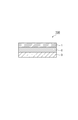
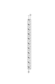
- FIG. 6 is an end view taken along line IV-IV in FIG. 5. It is a top view which shows one Embodiment of the adhesive agent pattern of this invention.
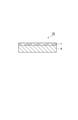
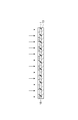
- FIG. 8 is an end view taken along line VV in FIG. 7. It is a top view which shows one Embodiment of the adhesive agent pattern of this invention.
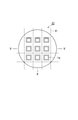
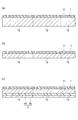
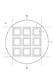
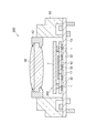
- FIG. 10 is an end view taken along line VI-VI in FIG. 9. It is an end elevation showing one embodiment of a semiconductor device of the present invention. It is an end elevation showing one embodiment of a semiconductor device of the present invention. It is an end view which shows one Embodiment of the manufacturing method of the semiconductor device of this invention. It is an end view which shows one Embodiment of the manufacturing method of the semiconductor device of this invention. It is a top view which shows one Embodiment of the manufacturing method of the semiconductor device of this invention. It is an end view which shows one Embodiment of the manufacturing method of the semiconductor device of this invention. It is an end view which shows one Embodiment of the manufacturing method of the semiconductor device of this invention. It is an end view which shows one Embodiment of the manufacturing method of the semiconductor device of this invention. It is an end view which shows one Embodiment of the manufacturing method of the semiconductor device of this invention.
- FIG. 27 is an end view showing an example of a CMOS sensor using the semiconductor device shown in FIG. 26 as a solid-state image sensor.
- the photosensitive adhesive composition according to the first embodiment of the present invention (hereinafter referred to as “first photosensitive adhesive composition”) has a minimum melt viscosity of 30000 Pa at 20 ° C. to 200 ° C. after pattern formation.
- -It is the photosensitive adhesive composition which is s or less.
- the “minimum melt viscosity” was measured using a viscoelasticity measuring device ARES (manufactured by Rheometrics Scientific F.E.) with a sample irradiated with a light amount of 1000 mJ / cm 2 .
- the minimum value of the melt viscosity at 20 ° C. to 200 ° C. is shown.
- the measurement plate is a parallel plate having a diameter of 8 mm, the measurement conditions are a temperature increase of 5 ° C./min, the measurement temperature is ⁇ 50 ° C. to 300 ° C., and the frequency is 1 Hz.
- the minimum melt viscosity is preferably 20000 Pa ⁇ s or less, more preferably 18000 Pa ⁇ s or less, and particularly preferably 15000 Pa ⁇ s or less.
- the first photosensitive adhesive composition can ensure sufficient low-temperature thermocompression bonding while controlling pattern deformation, and can be used for uneven substrates. Even good adhesion can be imparted.
- the lower limit of the minimum melt viscosity is not particularly provided, it is preferably 100 Pa ⁇ s or more from the viewpoint of handleability.
- the first photosensitive adhesive composition preferably contains (A) an alkali-soluble resin, (B) a thermosetting resin, (C) a radiation polymerizable compound, and (D) a photoinitiator.
- the average functional group equivalent of the (C) radiation polymerizable compound is preferably 230 g / eq or more, more preferably 245 g / eq or more, and 270 g / eq or more. Even more preferably.
- a radiation-polymerizable compound having a high functional group equivalent and making the average functional group equivalent of component (C) within the above range low stress, low warpage and low temperature thermocompression bonding can be improved.
- the minimum melt viscosity after pattern formation can be made 30000 Pa ⁇ s or less.
- the upper limit of the average functional group equivalent is not particularly provided, but the average functional group equivalent is preferably 1000 g / eq or less from the viewpoint of heat resistance reliability after development, adhesiveness, and moisture resistance reliability.
- Examples of the (C) radiation polymerizable compound contained in the first photosensitive adhesive composition include compounds having an unsaturated hydrocarbon group, and examples of the unsaturated hydrocarbon group include a vinyl group, an allyl group, and propargyl.
- Examples, butenyl group, ethynyl group, phenylethynyl group, maleimide group, nadiimide group, (meth) acryl group and the like, and (meth) acryl group is preferable from the viewpoint of reactivity.
- the (meth) acrylate having a (meth) acryl group is not limited, but diethylene glycol diacrylate, triethylene glycol diacrylate, tetraethylene glycol diacrylate, diethylene glycol dimethacrylate, triethylene glycol dimethacrylate, tetraethylene glycol dimethacrylate.
- polyimide resins polyamide polyurethane resins, polyamide imide resins, polyether imide resins, polyurethane resins, polyurethane imide resins, phenoxy resins, phenol resins, etc. are modified with unsaturated hydrocarbon groups on the side chains and / or terminals. Can be mentioned.
- R 19 and R 20 each independently represent a hydrogen atom or a methyl group, and g and h each independently represent an integer of 1 to 20.
- a vinyl copolymer containing a functional group to an addition reaction with a compound having at least one ethylenically unsaturated group and a functional group such as an oxirane ring, an isocyanate group, a hydroxyl group, or a carboxyl group.
- a radiation-polymerizable copolymer having an ethylenically unsaturated group in the chain can be used. These radiation polymerizable compounds can be used singly or in combination of two or more.
- the radiation-polymerizable compound having an ether skeleton represented by the general formula (18) is preferable in that it is alkali-soluble and can sufficiently impart solvent resistance after curing, (meth) acrylate having a urethane bond, Di (meth) acrylate and tri (meth) acrylate having an isocyanuric ring are preferable in that they can sufficiently impart high-temperature adhesiveness after curing.
- the component (C) preferably contains a (meth) acrylate having a urethane bond and / or an isocyanuric ring from the viewpoint of pattern formation and high temperature adhesiveness.
- the component (C) preferably contains a monofunctional (meth) acrylate.
- the 5% weight reduction temperature of the monofunctional (meth) acrylate is preferably 150 ° C. or higher.
- Such monofunctional (meth) acrylate is not particularly limited, but includes glycidyl group-containing (meth) acrylate, phenol EO-modified (meth) acrylate, phenol PO-modified (meth) acrylate, nonylphenol EO-modified (meth) acrylate, Nonylphenol PO modified (meth) acrylate, phenolic hydroxyl group-containing (meth) acrylate, hydroxyl group-containing (meth) acrylate, imide group-containing (meth) acrylate, carboxyl group-containing (meth) acrylate, 2-phenylphenoxyethyl (meth) acrylate, 5% weight loss temperature is 150 ° C.
- the 5% weight loss temperature is preferably 150 ° C. or higher, more preferably 180 ° C. or higher, even more preferably 200 ° C. or higher, and most preferably 260 ° C. or higher.
- the monofunctional (meth) acrylate is preferably a monofunctional (meth) acrylate having an epoxy group from the viewpoints of adhesiveness, low outgassing property, heat resistance and moisture resistance reliability.
- the monofunctional (meth) acrylate having an epoxy group is not particularly limited, but in addition to glycidyl methacrylate, glycidyl acrylate, 4-hydroxybutyl acrylate glycidyl ether, 4-hydroxybutyl methacrylate glycidyl ether, polyfunctional epoxy resin and epoxy group And a compound obtained by reacting a monofunctional (meth) acrylate having a functional group that reacts with.
- the monofunctional (meth) acrylate having an epoxy group is, for example, in the presence of triphenylphosphine or tetrabutylammonium bromide, a polyfunctional epoxy resin having at least two epoxy groups in one molecule, and 1 equivalent of an epoxy group. It is obtained by reacting with 0.1 to 0.9 equivalent of (meth) acrylic acid. Also, by reacting a polyfunctional isocyanate compound with a hydroxy group-containing (meth) acrylate and a hydroxy group-containing epoxy compound in the presence of dibutyltin dilaurate, or reacting a polyfunctional epoxy resin with an isocyanate group-containing (meth) acrylate. And glycidyl group-containing urethane (meth) acrylate and the like.
- the above monofunctional (meth) acrylate having an epoxy group has a 5% weight reduction temperature from the viewpoint of storage stability, adhesiveness, low outgassing of the package during assembly heating and after assembly, heat resistance and moisture resistance, and film formation. It is preferably 150 ° C. or higher in terms of suppressing volatilization or segregation on the surface due to heat drying at the time, and it is 180 ° C. or higher in terms of suppressing voids due to outgassing at the time of thermosetting, peeling, and adhesion deterioration. More preferably, it is still more preferable that it is 200 degreeC or more.
- a monofunctional (meth) acrylate having an epoxy group a compound having an aromatic ring in the molecule is preferable.
- the monofunctional (meth) acrylate having an epoxy group has a high purity in which alkali metal ions, alkaline earth metal ions, halogen ions, particularly chlorine ions and hydrolyzable chlorine, which are impurity ions, are reduced to 1000 ppm or less. It is preferable to use a product from the viewpoint of preventing electromigration and preventing corrosion of a metal conductor circuit.
- the impurities described above are used.
- the ion concentration can be satisfied.
- the total chlorine content can be measured according to JIS K7243-3.
- the glycidyl ether of bisphenol A type (or AD type, S type, F type), water addition bisphenol A type Glycidyl ether, ethylene oxide adduct bisphenol A and / or F type glycidyl ether, propylene oxide adduct bisphenol A and / or F type glycidyl ether, phenol novolac resin glycidyl ether, cresol novolac resin glycidyl ether, bisphenol A novolak resin Glycidyl ether, naphthalene resin glycidyl ether, trifunctional (or tetrafunctional) glycidyl ether, dicyclopentadienephenol resin glycidyl ether, dimer acid glycidyl ether Ether, 3 glycidylamine functional type (or tetrafunctional) g
- the monofunctional (meth) acrylate having such an epoxy group is not particularly limited, but compounds represented by the following general formulas (13) to (17) are preferably used.
- R 12 and R 16 represent a hydrogen atom or a methyl group
- R 10 , R 11 , R 13 and R 14 represent a divalent organic group
- R 15 to R 18 represent an epoxy group or an ethylenic group.
- An organic group having a saturated group is shown.
- the content of the component (C) is preferably 20 to 300 parts by mass, more preferably 30 to 250 parts by mass with respect to 100 parts by mass of the component (A).
- this content exceeds 300 parts by mass, the fluidity at the time of heat melting decreases due to polymerization, and the adhesiveness at the time of thermocompression bonding tends to decrease.
- it is less than 20 parts by mass, the solvent resistance after photocuring by exposure becomes low and it becomes difficult to form a pattern, that is, the change in film thickness before and after development increases and / or the residue increases. There is a tendency. Moreover, it melts at the time of thermocompression bonding and the pattern tends to be deformed.
- the content of the monofunctional (meth) acrylate having an epoxy group is not particularly limited as long as the minimum melt viscosity after pattern formation is 30000 Pa ⁇ s or less, but is 1 to 100 with respect to 100 parts by mass of the component (A). It is preferably part by mass, more preferably 2 to 70 parts by mass, and even more preferably 5 to 40 parts by mass. If this content exceeds 100 parts by mass, the thixotropy tends to decrease during film formation, and the film tends to be difficult to form, and the tack tends to increase and the handleability tends to be insufficient. Further, developability is reduced during pattern formation, and the pattern tends to be deformed during thermocompression bonding because the melt viscosity after photocuring is too low. On the other hand, when it is less than 1 part by mass, the effect of addition tends not to be sufficiently observed.
- the photosensitive adhesive composition according to the second embodiment of the present invention includes (A) an alkali-soluble resin, (B) a thermosetting resin, (C) A photosensitive adhesive composition containing a radiation polymerizable compound and (D) a photoinitiator, and the average functional group equivalent of the (C) radiation polymerizable compound is 230 g / eq or more.
- 2nd photosensitive adhesive composition becomes the thing excellent in all the points of low-temperature thermocompression-bonding property, low-temperature sticking property, high-temperature adhesiveness, and pattern formation property by containing the said component.
- the average functional group equivalent of the (C) radiation polymerizable compound is 230 g / eq or more, more preferably 245 g / eq or more, and more preferably 270 g / eq or more. Even more preferred.
- a radiation-polymerizable compound having a high functional group equivalent and making the average functional group equivalent of component (C) within the above range low stress, low warpage and low temperature thermocompression bonding can be improved.
- the minimum melt viscosity after heating at 150 ° C. for 10 minutes after pattern formation can be made 30000 Pa ⁇ s or less.
- the upper limit of the average functional group equivalent is not particularly provided, but the average functional group equivalent is preferably 1000 g / eq or less from the viewpoint of heat resistance reliability after development, adhesiveness, and moisture resistance reliability.
- the component (C) contained in the second photosensitive adhesive composition examples include compounds having an unsaturated hydrocarbon group exemplified in the first photosensitive resin composition.
- the component (C) preferably contains a (meth) acrylate having a urethane bond and / or an isocyanuric ring from the viewpoint of pattern formation and high-temperature adhesiveness. .
- the content of the component (C) in the second photosensitive adhesive composition is the same as that in the first photosensitive adhesive composition.
- the photosensitive adhesive composition according to the third embodiment of the present invention includes (A) a thermoplastic resin, (B) a thermosetting resin, (C) It is a photosensitive adhesive composition containing a radiation polymerizable compound and (D) a photoinitiator, and the (C) radiation polymerizable compound contains a compound having an ethylenically unsaturated group and an epoxy group.
- 3rd photosensitive adhesive composition becomes the thing excellent in all the points of low-temperature thermocompression-bonding property, low-temperature sticking property, high-temperature adhesiveness, and pattern formation property by containing the said component.
- the third photosensitive adhesive composition contains a thermoplastic resin having film-forming ability.
- Thermoplastic resin with film-forming ability has strong molecular entanglement and cohesion, so when the third photosensitive adhesive composition is used in paste form, it gives stability and thixotropy of the applied resin.
- a tough resin excellent in low stress property and adhesiveness after curing can be obtained.
- the film formability during coating can be improved, and defects such as resin seepage and pinholes can be improved.
- a tough resin excellent in low stress and adhesiveness can be obtained.
- component (A) when producing a film-like adhesive using a photosensitive adhesive composition containing a thermoplastic resin having film-forming ability, for example, as component (A), the following method may be used. It is preferable to use a resin that can form the film. 60 parts by mass of component (A) in a solvent selected from dimethylformamide, toluene, benzene, xylene, methyl ethyl ketone, tetrahydrofuran, ethyl cellosolve, ethyl cellosolve acetate, dioxane, cyclohexanone, ethyl acetate, and N-methyl-pyrrolidinone %, And coated on a PET film so that the film thickness after drying is 50 ⁇ m, heated in an oven at 80 ° C. for 20 minutes, and then heated at 120 ° C. for 20 minutes to form a film.
- a resin that can be formed is preferably used.
- thermoplastic resin is preferably an alkali-soluble resin from the viewpoint of pattern formation.
- the component (C) contains a compound having an ethylenically unsaturated group and an epoxy group, so that the crosslinking density can be reduced during photocuring, and low-temperature thermocompression bonding, low stress, and adhesiveness after photocuring. Further, after heat curing, the alkali resistance, solvent resistance and plating resistance are excellent.
- examples of the ethylenically unsaturated group include vinyl group, allyl group, propargyl group, butenyl group, ethynyl group, phenylethynyl group, maleimide group, nadiimide group, (meth) An acrylic group etc. are mentioned, From a reactive viewpoint, a (meth) acryl group is preferable.
- the compound having an ethylenically unsaturated group and an epoxy group is not particularly limited, but glycidyl methacrylate, glycidyl acrylate, 4-hydroxybutyl acrylate glycidyl ether, 4-hydroxybutyl methacrylate glycidyl ether, and other functional groups that react with epoxy groups. And a compound obtained by reacting a compound having a group and an ethylenically unsaturated group with a polyfunctional epoxy resin.
- An isocyanate group a carboxyl group, a phenolic hydroxyl group, a hydroxyl group, an acid anhydride, an amino group, a thiol group, an amide group etc. are mentioned. These compounds can be used individually by 1 type or in combination of 2 or more types.
- the compound having an ethylenically unsaturated group and an epoxy group is, for example, a polyfunctional epoxy resin having at least two epoxy groups in one molecule in the presence of triphenylphosphine or tetrabutylammonium bromide, and 1 equivalent of an epoxy group.
- a polyfunctional isocyanate compound with a hydroxy group-containing (meth) acrylate and a hydroxy group-containing epoxy compound in the presence of dibutyltin dilaurate or reacting a polyfunctional epoxy resin with an isocyanate group-containing (meth) acrylate.
- a compound having an ethylenically unsaturated group and an epoxy group has a 5% weight reduction temperature from the viewpoint of storage stability, adhesiveness, low outgassing of the package during and after assembly heating, and heat and humidity resistance, and film formation. It is preferably 150 ° C. or higher in terms of suppressing volatilization or segregation on the surface due to heat drying at the time, and it is 180 ° C. or higher in terms of suppressing voids due to outgassing at the time of thermosetting, peeling, and adhesion deterioration. More preferably, it is still more preferable that it is 200 degreeC or more.
- a compound having an ethylenically unsaturated group and an epoxy group a compound having an aromatic ring in the molecule is preferable.
- the compounds having an ethylenically unsaturated group and an epoxy group include high impurity ions, alkaline earth metal ions, halogen ions, particularly chlorine ions and hydrolyzable chlorine, which are reduced to 1000 ppm or less. It is preferable to use a pure product from the viewpoint of preventing electromigration and preventing corrosion of metal conductor circuits.
- the impurity ion concentration can be satisfied by using a polyfunctional epoxy resin with reduced alkali metal ions, alkaline earth metal ions, halogen ions, and the like as a raw material.
- the total chlorine content can be measured according to JIS K7243-3.
- Bisphenol A type (or AD type, S type, F type) glycidyl ether, water addition bisphenol A type Glycidyl ether, bisphenol A and / or F type glycidyl ether, propylene oxide adduct bisphenol A and / or F type glycidyl ether, glycidyl ether of phenol novolac resin, glycidyl ether of cresol novolac resin, bisphenol A novolak Glycidyl ether of resin, glycidyl ether of naphthalene resin, trifunctional (or tetrafunctional) glycidyl ether, glycidyl ether of dicyclopentadienephenol resin, glycidyl of dimer acid Ester, 3 glycidylamine functional type (or tetrafunctional) include
- the number of epoxy groups and ethylenically unsaturated groups of a compound having an ethylenically unsaturated group and an epoxy group is improved in order to improve the thermocompression bonding property, low stress property and adhesiveness, and maintain developability during pattern formation.
- Examples of the monofunctional (meth) acrylate having such an epoxy group include those exemplified in the first photosensitive adhesive composition.
- the content of the component (C) in the third photosensitive adhesive composition is the same as that in the first photosensitive adhesive composition.
- the content of the compound having an ethylenically unsaturated group and an epoxy group in the third photosensitive adhesive composition is preferably 1 to 100 parts by mass with respect to 100 parts by mass of component (A).
- the amount is more preferably part by mass, and further preferably 5 to 50 parts by mass. If this content exceeds 100 parts by mass, the thixotropy tends to be reduced during film formation, and film formation tends to be difficult, and tackiness tends to increase, resulting in insufficient handling properties. In addition, developability tends to be reduced during pattern formation, and the pattern tends to be deformed during thermocompression bonding because the melt viscosity after photocuring becomes too low. On the other hand, when the content of the compound having an ethylenically unsaturated group and an epoxy group is less than 1 part by mass, the effect of addition tends to be insufficient.
- the first and third photosensitive adhesive compositions further contain (E) a thermal radical generator.
- E a thermal radical generator.
- unreacted radiation-polymerizable compounds can be reduced by heat treatment after bonding, so generation of outgas in the package during assembly heating and after assembly can be sufficiently reduced, and the cured product can be uniformly made highly elastic. can do.
- a cured product having high heat resistance, low moisture permeability, and low moisture absorption can be obtained, and high-temperature adhesiveness and moisture resistance reliability are improved.
- the above composition is such that the reaction is difficult to proceed by coating drying when forming a pattern or a film, low temperature thermocompression after pattern formation or low temperature application when formed into a film Sex will be sufficient.
- the thermal radical generator is preferably an organic peroxide.
- an organic peroxide that has a high half-life temperature, high radical generation efficiency, and high solubility in a solvent as a thermal radical generator, the amount of unreacted radiation-polymerizable compounds in the photosensitive adhesive composition is further reduced. Can be made. Moreover, since it melt
- the minimum melt viscosity at 20 ° C. to 200 ° C. after pattern formation is preferably 30000 Pa ⁇ s or less, more preferably 20000 Pa ⁇ s or less, and 18000 Pa. -It is still more preferable that it is s or less, and it is still more preferable that it is 15000 Pa-s or less.
- the lower limit of the minimum melt viscosity is not particularly provided, it is preferably 100 Pa ⁇ s or more from the viewpoint of handleability.
- the first to third photosensitive adhesive compositions have good developability by containing an alkali-soluble resin as the component (A).
- the Tg of the component (A) is preferably 150 ° C. or less, more preferably ⁇ 20 ° C. to 150 ° C.
- the temperature for applying the film adhesive to the back surface of the wafer is preferably 20 to 150 ° C., more preferably 25 to 100 ° C., from the viewpoint of suppressing warpage of the semiconductor wafer.
- the Tg of the film adhesive is preferably set to 150 ° C. or lower. On the other hand, if Tg is less than ⁇ 20 ° C., the tackiness of the film surface in the B-stage state becomes too strong, and the handleability tends to be poor.
- Tg means the main dispersion peak temperature when the component (A) is formed into a film.
- RSA-2 viscoelasticity analyzer manufactured by Rheometrics Co., Ltd., measured under conditions of a heating rate of 5 ° C./min, a frequency of 1 Hz, and a measurement temperature of ⁇ 150 to 300 ° C.
- a tan ⁇ peak temperature near Tg was the main dispersion peak temperature.
- the weight average molecular weight of the component (A) is preferably controlled within the range of 5000 to 500,000, and is 10,000 to 300,000 from the viewpoint that the low temperature sticking property and the thermocompression bonding property and the high temperature adhesiveness can be highly compatible. Is more preferable, and is more preferably from 10,000 to 100,000 from the viewpoint of further improving the pattern formability. If the weight average molecular weight is within the above range, the strength, flexibility and tackiness of the photosensitive adhesive composition in the form of a sheet or film will be good, and the thermal fluidity will be good. It is possible to ensure good embedding property with respect to the wiring step (unevenness) on the substrate surface. When the weight average molecular weight is less than 5,000, the film formability tends to be insufficient.
- the weight average molecular weight means a weight average molecular weight when measured in terms of polystyrene using high performance liquid chromatography “C-R4A” (trade name) manufactured by Shimadzu Corporation.
- the temperature for attaching to the backside of the wafer can be kept low, and heating when the semiconductor element is bonded and fixed to the semiconductor element mounting support member
- the temperature (thermocompression bonding temperature) can also be lowered, and an increase in warpage of the semiconductor element can be suppressed.
- sticking property, thermocompression bonding property and developability can be effectively imparted.
- the “sticking property” means the sticking property when a film adhesive obtained by forming the photosensitive adhesive composition into a film is used.
- the component (A) (alkali-soluble resin)
- a polymer having an alkali-soluble group is preferable, and one having an alkali-soluble group at a terminal or a side chain is more preferable.
- the alkali-soluble group include an ethylene glycol group, a carboxyl group, a hydroxyl group, a sulfonyl group, and a phenolic hydroxyl group. These functional groups can be used alone or in combination of two or more.
- the component (A) is, for example, a thermoplastic resin having a carboxyl group and / or a hydroxyl group.
- polyester resin polyether resin, polyimide resin, polyamide resin, polyamideimide resin, polyetherimide resin, polyurethane resin, polyurethaneimide resin, polyurethaneamideimide resin, siloxane polyimide resin, polyester
- imide resins copolymers thereof, precursors thereof (polyamide acid, etc.)
- polybenzoxazole resins phenoxy resins, polysulfone resins, polyethersulfone resins, polyphenylene sulfide resins, polyester resins, polyether resins, polycarbonate resins And polyether ketone resins, (meth) acrylic copolymers having a weight average molecular weight of 10,000 to 1,000,000, novolak resins, phenol resins and the like.
- acrylic copolymers having a weight average molecular weight of 10,000 to 1,000,000, novolak resins, phenol resins and the like.
- an ether group, a carboxyl group, and / or a hydroxyl group may be added to
- the component (A) is preferably a polyimide resin and / or a polyamide-imide resin from the viewpoints of high-temperature adhesiveness, heat resistance, and film formability.
- the polyimide resin and / or the polyamideimide resin can be obtained, for example, by subjecting tetracarboxylic dianhydride and diamine to a condensation reaction by a known method. That is, in the organic solvent, tetracarboxylic dianhydride and diamine are equimolar, or if necessary, the total amount of diamine is preferably 0.00 with respect to the total 1.0 mol of tetracarboxylic dianhydride.
- the composition ratio is adjusted in the range of 5 to 2.0 mol, more preferably 0.8 to 1.0 mol (the order of addition of each component is arbitrary), and the addition reaction is performed at a reaction temperature of 80 ° C. or lower, preferably 0 to 60 ° C. .
- the viscosity of the reaction solution gradually increases, and polyamic acid, which is a polyimide resin precursor, is generated.
- said tetracarboxylic dianhydride is what recrystallized and refined with acetic anhydride.
- the amount of acid-terminated polyimide resin and / or polyamideimide resin oligomer tends to increase.
- the weight average molecular weight of the resin and / or the polyamide-imide resin tends to be low, and various properties including the heat resistance of the resin composition tend to be insufficient.
- the polyimide resin and / or the polyamideimide resin can be obtained by dehydrating and ring-closing the reaction product (polyamide acid).
- the dehydration ring closure can be performed by a thermal ring closure method in which heat treatment is performed, a chemical ring closure method using a dehydrating agent, or the like.
- the tetracarboxylic dianhydride used as a raw material for the polyimide resin and / or polyamideimide resin is not particularly limited.
- the tetracarboxylic dianhydride represented by the general formula (1) can be synthesized from, for example, trimellitic anhydride monochloride and the corresponding diol, specifically 1,2- (ethylene) bis ( Trimellitate anhydride), 1,3- (trimethylene) bis (trimellitic anhydride), 1,4- (tetramethylene) bis (trimellitate anhydride), 1,5- (pentamethylene) bis (trimellitate anhydride), 1 , 6- (Hexamethylene) bis (trimellitic anhydride), 1,7- (heptamethylene) bis (trimellitic anhydride), 1,8- (octamethylene) bis (trimellitic anhydride), 1,9- (nonamethylene) ) Bis (trimellitic anhydride), 1,10- (decamethylene) bis (trimellitate anhydrous), 1,12- (dodecamechi) Emissions) bis (trimellitate anhydride), 1,16 (hexamethylene decamethylene) bis (
- the tetracarboxylic dianhydride is a tetracarboxylic acid represented by the following general formula (2) or (3) from the viewpoint of imparting good solubility in solvents and moisture resistance, and transparency to 365 nm light.
- a dianhydride is preferred.
- tetracarboxylic dianhydrides can be used singly or in combination of two or more.
- the component (A) is preferably a carboxyl group and / or hydroxyl group-containing polyimide resin and / or a polyamideimide resin.
- the diamine used as a raw material for the carboxyl group and / or hydroxyl group-containing polyimide resin and / or polyamideimide resin is an aromatic diamine represented by the following general formula (4), (5), (6) or (7). It is preferable to include.
- the diamines represented by the following general formulas (4) to (7) are preferably 1 to 100 mol%, more preferably 3 to 80 mol%, and more preferably 5 to 50 mol% of the total diamine. Most preferably.
- diamines used as raw materials for the polyimide resin and / or polyamideimide resin are not particularly limited, and examples thereof include o-phenylenediamine, m-phenylenediamine, p-phenylenediamine, 3,3′-diaminodiphenyl ether, 3 , 4′-diaminodiphenyl ether, 4,4′-diaminodiphenyl ether, 3,3′-diaminodiphenylmethane, 3,4′-diaminodiphenylmethane, 4,4′-diaminodiphenylethermethane, bis (4-amino-3,5- Dimethylphenyl) methane, bis (4-amino-3,5-diisopropylphenyl) methane, 3,3′-diaminodiphenyldifluoromethane, 3,4′-diaminodiphenyldifluoromethane, 4,4′-
- Aromatic diamines 1,3-bis (aminomethyl) cyclohexane, 2,2-bis (4-aminophenoxyphenyl) propane, aliphatic ether diamines represented by the following general formula (8), -1), and siloxane diamines represented by the following general formula (9).
- R 1 , R 2 and R 3 each independently represents an alkylene group having 1 to 10 carbon atoms, and b represents an integer of 1 to 80.
- c represents an integer of 5 to 20.
- the aliphatic ether diamines represented by the above general formula (8) are preferable in terms of imparting compatibility with other components, organic solvent solubility, and alkali solubility, and ethylene glycol and / or propylene glycol diamines. Is more preferable.
- aliphatic ether diamines include Jeffamine D-230, D-400, D-2000, D-4000, ED-600, ED-900, ED-2000, and EDR manufactured by Sun Techno Chemical Co., Ltd. 148, aliphatic diamines such as polyoxyalkylene diamines such as polyetheramine D-230, D-400, D-2000 and the like. These diamines are preferably 1 to 80 mol% of the total diamine, and are 5 to 60 mol in terms of compatibility with other compounding components and high compatibility between low temperature sticking property, thermocompression bonding property and high temperature adhesiveness. % Is more preferable.
- this amount is less than 1 mol%, it tends to be difficult to impart high-temperature adhesiveness and hot fluidity. On the other hand, if it exceeds 80 mol%, the Tg of the polyimide resin becomes too low, Self-supporting tends to be impaired.
- the siloxane diamine represented by following General formula (9) is preferable at the point which provides the adhesiveness and adhesiveness in room temperature.
- R 4 and R 9 each independently represents an alkylene group having 1 to 5 carbon atoms or a phenylene group which may have a substituent
- Each of 8 independently represents an alkyl group having 1 to 5 carbon atoms, a phenyl group or a phenoxy group
- d represents an integer of 1 to 5.
- These diamines are preferably used in an amount of 0.5 to 80 mol% of the total diamine, and more preferably 1 to 50 mol% in terms of achieving a high degree of compatibility between low temperature sticking property, thermocompression bonding property and high temperature adhesiveness. .
- the amount is less than 0.5 mol%, the effect of adding siloxane diamine is reduced.
- the amount exceeds 80 mol%, the compatibility with other components, high-temperature adhesiveness, and developability tend to be lowered.
- d in the formula (9) is 1, 1,1,3,3-tetramethyl-1,3-bis (4- Aminophenyl) disiloxane, 1,1,3,3-tetraphenoxy-1,3-bis (4-aminoethyl) disiloxane, 1,1,3,3-tetraphenyl-1,3-bis (2- Aminoethyl) disiloxane, 1,1,3,3-tetraphenyl-1,3-bis (3-aminopropyl) disiloxane, 1,1,3,3-tetramethyl-1,3-bis (2- Aminoethyl) disiloxane, 1,1,3,3-tetramethyl-1,3-bis (3-aminopropyl) disiloxane, 1,1,3,3-tetramethyl-1,3-bis (3- Aminobutyl) disiloxane, 1,3-dimethyl-1,3 Examples include dime
- diamines can be used singly or in combination of two or more.
- the said polyimide resin and / or a polyamide-imide resin can be used individually by 1 type or in mixture (blend) of 2 or more types as needed.
- the Tg when determining the composition of the polyimide resin and / or the polyamideimide resin, it is preferable to design the Tg to be 150 ° C. or less. It is particularly preferable to use an aliphatic ether diamine represented by the general formula (8).
- a monofunctional acid anhydride and / or a monofunctional amine such as a compound represented by the following general formula (10), (11) or (12) is condensed into a reaction solution. It is possible to introduce a functional group other than an acid anhydride or a diamine at the polymer terminal. Thereby, the molecular weight of the polymer can be lowered, and the developability and thermocompression property at the time of pattern formation can be improved.
- Alkali-soluble groups such as a carboxyl group, a phenolic hydroxyl group, and an ether group, are preferable at the point which improves the alkali solubility at the time of pattern formation.
- the compound which has radiation-polymerizable groups and / or thermosetting groups such as the compound represented by following General formula (12), and the (meth) acrylate which has an amino group, is preferably used at the point which provides adhesiveness.
- a compound having a siloxane skeleton or the like is also preferably used in terms of imparting low hygroscopicity.
- the polyimide resin and / or the polyamideimide resin has a transmittance of 365 nm when formed into a film of 30 ⁇ m, and is 10% or more in that the side wall of the pattern is perpendicular to the adherend. It is preferable that it is 20% or more because a pattern can be formed with a lower exposure amount.
- a polyimide resin is represented by, for example, an acid anhydride represented by the general formula (2), an aliphatic ether diamine represented by the general formula (8), and / or the general formula (9). It can be synthesized by reacting with siloxane diamine.
- the content of the component (A) is preferably 5 to 90% by mass, and 20 to 80% by mass based on the total solid content of the photosensitive adhesive composition. It is more preferable that If the content is less than 20% by mass, the developability during pattern formation tends to be insufficient, and if it exceeds 80% by mass, the developability and adhesiveness during pattern formation tend to be insufficient.
- a resin having a carboxyl group and / or a hydroxyl group and / or a resin having a hydrophilic group is added as a dissolution aid. May be.
- the resin having a hydrophilic group is not particularly limited as long as it is an alkali-soluble resin, and examples thereof include resins having glycol groups such as ethylene glycol and propylene glycol groups.
- the thermosetting resin preferably contains at least two epoxy groups in the molecule, and phenol and phenol are preferable from the viewpoint of curability and cured product characteristics.
- the glycidyl ether type epoxy resin is more preferable.
- examples of such resins include bisphenol A type (or AD type, S type, and F type) glycidyl ether, water-added bisphenol A type glycidyl ether, ethylene oxide adduct bisphenol A type glycidyl ether, and propylene oxide adduct.
- thermosetting resin is a high-purity product in which impurity ions such as alkali metal ions, alkaline earth metal ions, halogen ions, particularly chlorine ions and hydrolyzable chlorine are reduced to 300 ppm or less. It is preferable to use it from the viewpoint of preventing electromigration and preventing corrosion of a metal conductor circuit.
- the content of the component (B) is preferably 0.1 to 100 parts by mass and more preferably 2 to 50 parts by mass with respect to 100 parts by mass of the component (A).
- this content exceeds 100 parts by mass, the solubility in an alkaline aqueous solution is lowered, and the pattern formability tends to be insufficient.
- the content is less than 0.1 parts by mass, the high-temperature adhesiveness tends to be insufficient.
- a curing agent In addition to the component (B), a curing agent, a curing accelerator, a radiation polymerizable compound, and the like may be included.
- the curing agent examples include phenolic compounds, aliphatic amines, alicyclic amines, aromatic polyamines, polyamides, aliphatic acid anhydrides, alicyclic acid anhydrides, aromatic acid anhydrides, dicyandiamide, and organic acid dihydrazides. , Boron trifluoride amine complexes, imidazoles, tertiary amines and the like. Among these, phenol compounds are preferable, and phenol compounds having at least two phenolic hydroxyl groups in the molecule are more preferable.
- Examples of such compounds include phenol novolak, cresol novolak, t-butylphenol novolak, dicyclopentadiene cresol novolak, dicyclopentadienephenol novolak, xylylene-modified phenol novolak, naphthol compound, trisphenol compound, tetrakisphenol novolak, bisphenol.
- a novolak, poly-p-vinylphenol, phenol aralkyl resin and the like those having a number average molecular weight in the range of 400 to 4000 are preferable. Thereby, the outgas at the time of heating which causes the contamination of the semiconductor element or the device at the time of assembling the semiconductor device can be suppressed.
- the content of the phenolic compound is preferably 1 to 100 parts by weight, more preferably 2 to 50 parts by weight, and more preferably 2 to 30 parts by weight with respect to 100 parts by weight of component (A). Most preferred.
- this content exceeds 100 parts by mass, the reactivity of the compound having an ethylenically unsaturated group and epoxy group and the radiation polymerizable compound at the time of exposure becomes poor, or the acid value and phenolic hydroxyl value of the resin increase.
- the film thickness tends to decrease or swell after development.
- the penetration of the developer into the resin pattern increases, outgassing during subsequent heat curing and assembly heat history tends to increase, and heat resistance reliability and moisture resistance reliability tend to be greatly reduced.
- the content is less than 1 part by mass, there is a tendency that sufficient high-temperature adhesiveness cannot be obtained.
- the curing accelerator is not particularly limited as long as it contains a curing accelerator that accelerates curing / polymerization of epoxy by heating.
- a curing accelerator that accelerates curing / polymerization of epoxy by heating.
- examples include tetraphenylborate, 2-ethyl-4-methylimidazole-tetraphenylborate, 1,8-diazabicyclo [5.4.0] undecene-7-tetraphenylborate.
- the content of the curing accelerator in the photosensitive adhesive composition is preferably 0.01 to 50 parts by mass with respect to 100 parts by mass of the epoxy resin.
- the component (D) (photoinitiator) has a molecular extinction coefficient of 1000 ml / g ⁇ cm or more for light having a wavelength of 365 nm from the viewpoint of improving sensitivity. And more preferably 2000 ml / g ⁇ cm or more.
- a 0.001 mass% acetonitrile solution of the sample is prepared, and the absorbance of this solution is measured using a spectrophotometer (manufactured by Hitachi High-Technologies Corporation, “U-3310” (trade name)). Is required.
- the component (D) is more preferably bleached by light irradiation.
- Examples of such component (D) include 2-benzyl-2-dimethylamino-1- (4-morpholinophenyl) -butanone-1,2,2-dimethoxy-1,2-diphenylethane-1-one.
- Benzyl derivatives such as aromatic ketones, benzyldimethyl ketal, 2- (o-chlorophenyl) -4,5-diphenylimidazole dimer, 2- (o-chlorophenyl) -4,5-di (m-methoxyphenyl) imidazole Dimer, 2- (o-fluorophenyl) -4,5-phenylimidazole dimer, 2- (o Methoxyphenyl) -4,5-diphenylimidazole dimer, 2- (p-methoxyphenyl) -4,5-diphenylimidazole dimer, 2,4-di (p-methoxyphenyl) -5-phenylimidazole dimer 2,4,5-triarylimidazole dimers such as 2- (2,4-dimethoxyphenyl) -4,5-diphenylimidazole dimer, 9-phenylacridine, 1,7-bis (9 , 9'-acridinyl) h
- the component may contain the photoinitiator which expresses the function which accelerates
- a photoinitiator include a photobase generator that generates a base by irradiation, a photoacid generator that generates an acid by irradiation, and the photobase generator is particularly preferable.
- the photobase generator By using the photobase generator, the high-temperature adhesion and moisture resistance of the photosensitive adhesive composition to the adherend can be further improved. This is because the base generated from the photobase generator acts as a curing catalyst for the epoxy resin efficiently, so that the crosslinking density can be further increased, and the generated curing catalyst corrodes the substrate and the like. This is thought to be because there are few. Moreover, by including a photobase generator in the photosensitive adhesive composition, the crosslink density can be improved, and the outgas during standing at high temperature can be further reduced. Furthermore, it is considered that the curing process temperature can be lowered and shortened.
- the photosensitive adhesive composition containing a photobase generator a base is generated by irradiation of the radiation, whereby the carboxyl remaining after the reaction of the above carboxyl group and / or hydroxyl group with the epoxy resin.
- the group and / or hydroxyl group can be reduced, and it becomes possible to achieve a higher level of moisture resistance, adhesion and pattern formation.
- the photobase generator can be used without particular limitation as long as it is a compound that generates a base upon irradiation with radiation.
- a strongly basic compound is preferable in terms of reactivity and curing speed.
- a pKa value that is a logarithm of an acid dissociation constant is used as a basic index, and a base having a pKa value in an aqueous solution of 7 or more is preferable, and a base of 9 or more is more preferable.
- Examples of the base generated upon irradiation with radiation include imidazole derivatives such as imidazole, 2,4-dimethylimidazole, and 1-methylimidazole, piperazine derivatives such as piperazine and 2,5-dimethylpiperazine, piperidine, 1,2, and the like.
- -A piperidine derivative such as dimethylpiperidine, a proline derivative, a trialkylamine derivative such as trimethylamine, triethylamine or triethanolamine, an amino group or an alkylamino group substituted at the 4-position of 4-methylaminopyridine, 4-dimethylaminopyridine, etc.
- Pyridine derivatives such as pyrrolidine, n-methylpyrrolidine, dihydropyridine derivatives, triethylenediamine, alicyclic amine derivatives such as 1,8-diazabiscyclo (5,4,0) undecene-1 (DBU) Body, benzyl methyl amine, benzyl dimethyl amine, and the like benzylamine derivatives such as benzyl diethylamine.
- pyrrolidine derivatives such as pyrrolidine, n-methylpyrrolidine, dihydropyridine derivatives, triethylenediamine, alicyclic amine derivatives such as 1,8-diazabiscyclo (5,4,0) undecene-1 (DBU) Body, benzyl methyl amine, benzyl dimethyl amine, and the like benzylamine derivatives such as benzyl diethylamine.
- the photobase generator a compound in which a group capable of generating a base is introduced into the main chain and / or side chain of the polymer may be used.
- the molecular weight in this case is preferably a weight average molecular weight of 1,000 to 100,000, more preferably 5,000 to 30,000, from the viewpoints of adhesiveness, fluidity and heat resistance as an adhesive.
- the above-mentioned photobase generator does not show reactivity with the epoxy resin in a state where it is not irradiated with radiation at room temperature, and therefore has excellent storage stability at room temperature.
- a thermal radical generator can be used as necessary.
- the thermal radical generator is preferably an organic peroxide.
- the organic peroxide preferably has a one minute half-life temperature of 120 ° C. or higher, more preferably 150 ° C. or higher.
- the organic peroxide is selected in consideration of preparation conditions of the photosensitive adhesive composition, film forming temperature, curing (bonding) conditions, other process conditions, storage stability, and the like.
- the peroxide that can be used is not particularly limited.
- thermal radical generators include, for example, perhexa 25B (manufactured by NOF Corporation), 2,5-dimethyl-2,5-di (t-butylperoxyhexane) (1 minute) Half-life temperature: 180 ° C., Park mill D (manufactured by NOF Corporation), dicumyl peroxide (1 minute half-life temperature: 175 ° C.), and the like.
- the addition amount of the thermal radical generator is preferably 0.01 to 20% by weight, more preferably 0.1 to 10% by weight, more preferably 0.5 to 4% by weight based on the total amount of the compound having an ethylenically unsaturated group. 5% by weight is most preferred. If it is 0.01% by weight or less, the curability is lowered and the effect of addition is reduced, and if it exceeds 5% by weight, the outgas amount is increased and the storage stability is lowered.
- a sensitizer can be used in combination as necessary.
- the sensitizer include camphorquinone, benzyl, diacetyl, benzyldimethyl ketal, benzyldiethyl ketal, benzyldi (2-methoxyethyl) ketal, 4,4′-dimethylbenzyl-dimethyl ketal, anthraquinone, 1-chloroanthraquinone.
- quinones In order to impart storage stability, process adaptability or antioxidant properties to the first to third photosensitive adhesive compositions, quinones, polyhydric phenols, phenols, phosphites, sulfurs, etc.
- a polymerization inhibitor or an antioxidant may be further added as long as the curability is not impaired.
- the above-mentioned photosensitive adhesive composition can contain a filler as appropriate.
- the filler include metal fillers such as silver powder, gold powder, copper powder, and nickel powder, alumina, aluminum hydroxide, magnesium hydroxide, calcium carbonate, magnesium carbonate, calcium silicate, magnesium silicate, calcium oxide, magnesium oxide, Inorganic fillers such as aluminum oxide, aluminum nitride, crystalline silica, amorphous silica, boron nitride, titania, glass, iron oxide, and ceramics, and organic fillers such as carbon and rubber fillers are included. Regardless, it can be used without any particular restrictions.
- the filler can be used properly according to the desired function.
- a metal filler is added for the purpose of imparting conductivity, thermal conductivity, thixotropy, etc. to the resin composition
- a nonmetallic inorganic filler is added to the adhesive layer for thermal conductivity, low thermal expansion, low hygroscopicity, etc.
- the organic filler is added for the purpose of imparting toughness to the adhesive layer.
- metal fillers, inorganic fillers or organic fillers can be used singly or in combination of two or more.
- metal fillers, inorganic fillers, or insulating fillers are preferable in terms of being able to impart conductivity, thermal conductivity, low moisture absorption characteristics, insulating properties, and the like required for adhesive materials for semiconductor devices, and inorganic fillers or insulating fillers.
- a silica filler is more preferable in that it has good dispersibility with respect to the resin varnish and can impart a high adhesive force when heated.
- the filler preferably has an average particle size of 10 ⁇ m or less and a maximum particle size of 30 ⁇ m or less, more preferably an average particle size of 5 ⁇ m or less and a maximum particle size of 20 ⁇ m or less.
- the average particle diameter exceeds 10 ⁇ m and the maximum particle diameter exceeds 30 ⁇ m, the effect of improving fracture toughness tends to be insufficient.
- the lower limits of the average particle size and the maximum particle size are not particularly limited, but usually both are 0.001 ⁇ m.
- the content of the filler is determined according to the properties or functions to be imparted, but is preferably 0 to 50% by mass, more preferably 1 to 40% by mass, and more preferably 3 to 30% by mass with respect to the total of the resin component and the filler. Is more preferable.
- a high elastic modulus can be achieved, and dicing properties (cutability by a dicer blade), wire bonding properties (ultrasonic efficiency), and adhesive strength during heating can be effectively improved.
- the filler content is preferably within the above range.
- the optimum filler content is determined in order to balance the required properties. Mixing and kneading in the case of using a filler can be carried out by appropriately combining dispersers such as ordinary stirrers, raking machines, three rolls, and ball mills.
- Various coupling agents can be added to the photosensitive adhesive composition in order to improve interfacial bonding between different materials.
- the coupling agent include silane-based, titanium-based, and aluminum-based.
- a silane-based coupling agent is preferable because of its high effect, and a thermosetting group such as an epoxy group, methacrylate, and / or acrylate.
- a compound having a radiation polymerizable group such as is more preferred.
- the boiling point and / or decomposition temperature of the silane coupling agent is preferably 150 ° C. or higher, more preferably 180 ° C. or higher, and even more preferably 200 ° C. or higher. That is, a silane coupling agent having a boiling point of 200 ° C.
- the amount of the coupling agent used is preferably 0.01 to 20 parts by mass with respect to 100 parts by mass of the component (A) to be used, from the viewpoints of the effect, heat resistance and cost.
- an ion scavenger can be further added in order to adsorb ionic impurities and improve insulation reliability during moisture absorption.
- an ion scavenger is not particularly limited.
- triazine thiol compound a compound known as a copper damage preventer for preventing copper from being ionized and dissolved, such as a phenol-based reducing agent, Inorganic compounds such as bismuth-based, antimony-based, magnesium-based, aluminum-based, zirconium-based, calcium-based, titanium-based, zuzu-based, and mixed systems thereof.
- IXE-300 antimony type
- IXE-500 bismuth type
- IXE-600 antimony, bismuth mixed type
- IXE-700 magnesium and aluminum mixed system
- IXE-800 zirconium system
- IXE-1100 calcium system
- the amount of the ion scavenger used is preferably 0.01 to 10 parts by mass with respect to 100 parts by mass of component (A) from the viewpoints of the effect of addition, heat resistance, cost, and the like.
- a film adhesive can be obtained by forming the first to third photosensitive adhesive compositions into a film.
- FIG. 1 is an end view showing an embodiment of the film adhesive of the present invention.
- a film adhesive 1 shown in FIG. 1 is obtained by forming the photosensitive adhesive composition into a film.
- the film-like adhesive 1 is formed into a film shape by, for example, applying the photosensitive adhesive composition on the substrate 3 shown in FIG. 2 and drying it.
- the adhesive sheet 100 provided with the base material 3 and the adhesive layer 1 made of the film-like adhesive formed on the base material 3 is obtained.
- FIG. 2 is an end view showing an embodiment of the adhesive sheet 100 of the present invention.
- the adhesive sheet 100 shown in FIG. 2 is comprised from the base material 3 and the adhesive bond layer 1 which consists of a film adhesive provided on the one side.
- FIG. 3 is an end view showing another embodiment of the adhesive sheet of the present invention.
- the adhesive sheet 100 shown in FIG. 3 is comprised from the base material 3, the adhesive bond layer 1 and cover film 2 which consist of a film adhesive provided on the one side of this.
- the component (A), the component (B), the component (C), the component (D) and other components added as necessary are mixed in an organic solvent, and the mixed solution is kneaded.
- the varnish can be prepared by applying the varnish on the base material 3 to form a varnish layer, drying the varnish layer by heating, and then removing the base material 3. At this time, the substrate 3 can be stored or used in the state of the adhesive sheet 100 without removing the substrate 3.
- the organic solvent used for preparing the varnish is not particularly limited as long as the material can be uniformly dissolved or dispersed.
- examples include dimethylformamide, toluene, benzene, xylene, methyl ethyl ketone, tetrahydrofuran, ethyl cellosolve, ethyl cellosolve acetate, dioxane, cyclohexanone, ethyl acetate, and N-methyl-pyrrolidinone.
- the above mixing and kneading can be performed by appropriately combining dispersers such as a normal stirrer, a raking machine, a three-roller, and a ball mill.
- the drying by heating is performed at a temperature at which the component (B) does not sufficiently react and the solvent is sufficiently volatilized.
- the “temperature at which the component (B) does not sufficiently react” refers to DSC (for example, “DSC-7 type” (trade name) manufactured by PerkinElmer, Inc.), sample amount: 10 mg
- the temperature is equal to or lower than the peak temperature of the heat of reaction when measured under the conditions of temperature rising rate: 5 ° C./min and measurement atmosphere: air.
- the varnish layer is dried usually by heating at 60 to 180 ° C. for 0.1 to 90 minutes.
- the preferred thickness of the varnish layer before drying is 1 to 200 ⁇ m. If this thickness is less than 1 ⁇ m, the adhesive fixing function tends to be insufficient, and if it exceeds 200 ⁇ m, the residual volatile matter described later tends to increase.
- the preferred residual volatile content of the obtained varnish layer is 10% by mass or less. If this residual volatile content exceeds 10% by mass, voids tend to remain inside the adhesive layer due to foaming due to solvent volatilization during assembly heating, and the moisture resistance tends to be insufficient. Moreover, there is a tendency that peripheral materials or members are contaminated by volatile components generated during heating.
- the measurement conditions of said residual volatile component are as follows. That is, for the film-like adhesive 1 cut to a size of 50 mm ⁇ 50 mm, the initial mass is M1, and the mass after heating the film-like adhesive 1 in an oven at 160 ° C. for 3 hours is M2, and the following formula To obtain the remaining volatile content (%).
- Formula Residual volatile content (%) [(M2-M1) / M1] ⁇ 100
- the substrate 3 is not particularly limited as long as it can withstand the above drying conditions.
- a polyester film, a polypropylene film, a polyethylene terephthalate film, a polyimide film, a polyetherimide film, a polyether naphthalate film, or a methylpentene film can be used as the substrate 3.
- the film as the substrate 3 may be a multilayer film in which two or more kinds are combined, or the surface may be treated with a release agent such as a silicone or silica.
- the film adhesive 1 and the dicing sheet can be laminated to form an adhesive sheet.
- the dicing sheet is a sheet provided with a pressure-sensitive adhesive layer on a substrate, and the pressure-sensitive adhesive layer may be either a pressure-sensitive type or a radiation curable type.
- the base material is preferably a base material that can be expanded.
- FIG. 5 is a top view showing an embodiment of a semiconductor wafer with an adhesive layer of the present invention
- FIG. 6 is an end view taken along the line IV-IV in FIG.
- a semiconductor wafer 20 with an adhesive layer shown in FIGS. 5 and 6 includes a semiconductor wafer 8 and a film adhesive (adhesive layer) 1 provided on one surface thereof.
- the semiconductor wafer 20 with an adhesive layer is obtained by laminating the film adhesive 1 on the semiconductor wafer 8 while heating.
- the film adhesive 1 can be attached to the semiconductor wafer 8 at a low temperature of about room temperature (25 ° C.) to 150 ° C., for example.
- FIGS. 7, 8, 9 and 10 are respectively a top view showing an embodiment of the adhesive pattern of the present invention
- FIG. 8 is an end view taken along the line VV of FIG. 7
- FIG. FIG. 6 is an end view taken along the line VI.
- the adhesive pattern 1a shown in FIGS. 7, 8, 9 and 10 is formed on the semiconductor wafer 8 as the adherend so as to have a pattern along a substantially square side or a square pattern.
- the adhesive pattern 1a is obtained by laminating the adhesive layer 1 on a semiconductor wafer 8 as an adherend to obtain a semiconductor wafer 20 with an adhesive layer, exposing the adhesive layer 1 through a photomask, and after exposure.
- the adhesive layer 1 is developed by an alkaline developer. Thereby, the semiconductor wafer 20 with an adhesive layer in which the adhesive pattern 1a is formed is obtained.
- FIG. 11 is an end view showing an embodiment of the semiconductor device of the present invention.
- the semiconductor element 12 is bonded to the semiconductor element mounting support member 13 via the film adhesive 1, and the connection terminal (not shown) of the semiconductor element 12 is externally connected via the wire 14. It is electrically connected to a connection terminal (not shown) and sealed with a sealing material 15.
- FIG. 12 is an end view showing another embodiment of the semiconductor device of the present invention.
- the first-stage semiconductor element 12a is bonded to the semiconductor-element mounting support member 13 on which the terminals 16 are formed via the film adhesive 1
- the first-stage semiconductor element 12a is bonded to the first-stage semiconductor element 12a.
- a second-stage semiconductor element 12b is bonded via a film adhesive 1.
- the connection terminals (not shown) of the first-stage semiconductor element 12a and the second-stage semiconductor element 12b are electrically connected to the external connection terminals via the wires 14, and are sealed with a sealing material.
- the film adhesive of the present invention can be suitably used for a semiconductor device having a structure in which a plurality of semiconductor elements are stacked.
- the semiconductor wafer 20 with the adhesive layer shown in FIG. 9 is diced along the broken line D, and the semiconductor element with the adhesive layer after dicing is mounted on the semiconductor element. It can be obtained by thermocompression bonding to the supporting member 13 and bonding them together, followed by steps such as a wire bonding step and, if necessary, a sealing step with a sealing material.
- the heating temperature in the thermocompression bonding is usually 20 to 250 ° C.
- the load is usually 0.01 to 20 kgf
- the heating time is usually 0.1 to 300 seconds.
- FIG. 18 there is a semiconductor device according to an embodiment of the present invention as shown in FIG.
- a method for manufacturing the semiconductor device shown in FIG. 18 will be described in detail with reference to the drawings.
- 13, 14 and 16 to 19 are end views showing an embodiment of a method for manufacturing a semiconductor device of the present invention
- FIG. 15 is a top view showing an embodiment of a method for manufacturing a semiconductor device of the present invention. .
- the manufacturing method of the semiconductor device of the present embodiment includes the following (Step 1) to (Step 7).
- Step 1) Step of laminating a film adhesive (adhesive layer) 1 on the circuit surface 18 of the semiconductor chip (semiconductor element) 12 formed in the semiconductor wafer 8 (FIGS. 13A and 13B) .
- Step 2) A step of patterning the adhesive layer 1 provided on the circuit surface 18 of the semiconductor chip 12 by exposure and development (FIGS. 13C and 14A).
- Step 3) A step of thinning the semiconductor wafer 8 by polishing the semiconductor wafer 8 from the surface opposite to the circuit surface 18 (FIG. 14B).
- Step 4 A step of dicing the semiconductor wafer 8 into a plurality of semiconductor chips 12 by dicing (FIGS. 14C and 16A).
- Step 5 A step of picking up the semiconductor chip 12 and mounting it on a plate-like support member (semiconductor element mounting support member) 13 for a semiconductor device (FIGS. 16B and 17A).
- Step 6) A step of laminating the second semiconductor chip 12b on the adhesive layer 1 patterned on the circuit surface 18 of the semiconductor chip 12a mounted on the support member 13 (FIG. 17B).
- Step 7) A step of connecting the semiconductor chips 12a and 12b to the external connection terminals, respectively (FIG. 18).
- Step 1 In the semiconductor wafer 8 shown in FIG. 13A, a plurality of semiconductor chips 12 divided by dicing lines D are formed. A film adhesive (adhesive layer) 1 is laminated on the surface of the semiconductor chip 12 on the circuit surface 18 side (FIG. 13B).
- a method of laminating the adhesive layer 1 a method of preparing a film-like adhesive previously formed into a film shape and affixing it to the semiconductor wafer 8 is simple, but it is liquid using a spin coat method or the like. A method of applying a varnish of a photosensitive adhesive composition to the semiconductor wafer 8 and drying by heating may be used.
- the adhesive layer 1 is a negative photosensitive adhesive that has adhesiveness to an adherend after being patterned by exposure and development and is capable of alkali development. More specifically, a resist pattern (adhesive pattern) formed by patterning the adhesive layer 1 by exposure and development has adhesion to an adherend such as a semiconductor chip or a support member. For example, the adhesive pattern and the adherend can be bonded to each other by pressing the adherend to the adhesive pattern while heating if necessary.
- Actinic rays (typically ultraviolet rays) are irradiated to the adhesive layer 1 laminated on the semiconductor wafer 8 through the mask 4 having openings at predetermined positions (FIG. 13C). Thereby, the adhesive layer 1 is exposed in a predetermined pattern.
- the adhesive layer 1 is patterned so that the opening 11 is formed by removing the unexposed portion of the adhesive layer 1 by development using an alkaline developer (FIG. 14A).
- an alkaline developer FIG. 14A
- FIG. 15 is a top view showing a state where the adhesive layer 1 is patterned.
- the bonding pad of the semiconductor chip 12 is exposed. That is, the patterned adhesive layer 1 is a buffer coat film of the semiconductor chip 12.
- a plurality of rectangular openings 11 are formed side by side on each semiconductor chip 12. The shape, arrangement, and number of the openings 11 are not limited to those in the present embodiment, and can be appropriately modified so that a predetermined portion such as a bonding pad is exposed.
- 14 is an end view taken along the line II-II in FIG.
- polishing is performed, for example, by attaching an adhesive film on the adhesive layer 1 and fixing the semiconductor wafer 8 to a polishing jig with the adhesive film.
- the semiconductor wafer 8 is cut along with the adhesive layer 1 and the composite film 5 along the dicing line D. Thereby, a plurality of semiconductor chips 12 each having the adhesive layer 1 and the composite film are obtained (FIG. 16A).
- This dicing is performed using a dicing blade in a state where the whole is fixed to the frame by the dicing tape 40, for example.
- Step 6 A second semiconductor chip 12b is stacked on the adhesive layer 1 on the semiconductor chip 12a mounted on the support member 13 (FIG. 17B). That is, the semiconductor chip 12a and the semiconductor chip 12b located in an upper layer thereof are bonded by the patterned adhesive layer 1 (buffer coat film) interposed therebetween. The semiconductor chip 12b is bonded to a position where the opening 11 is not blocked in the patterned adhesive layer 1. A patterned adhesive layer 1 (buffer coat film) is also formed on the circuit surface 18 of the semiconductor chip 12b.
- the bonding of the semiconductor chip 12b is performed, for example, by a method of thermocompression bonding while heating to a temperature at which the adhesive layer 1 exhibits fluidity. After the thermocompression bonding, the adhesive layer 1 is heated as necessary to further cure.
- Step 7 Thereafter, the semiconductor chip 12a is connected to an external connection terminal on the support member 13 via a wire 14a connected to the bonding pad, and the semiconductor chip 12b is connected to the support member 13 via a wire 14b connected to the bonding pad. Connected to the external connection terminal.
- the stacked body including the semiconductor chips 12a and 12b is sealed with the sealing material 15 to obtain the semiconductor device 200 (FIG. 18).
- the manufacturing method of the semiconductor device of the present invention is not limited to the above embodiment, and can be appropriately changed without departing from the gist of the present invention.
- the order of (Step 1) to (Step 7) can be changed as appropriate.
- dicing may be performed after the semiconductor wafer 8 on which the adhesive layer 1 is formed is thinned by polishing.
- the adhesive layer 1 is patterned by exposure and development to obtain a laminate similar to that shown in FIG.
- the semiconductor wafer may be thinned by polishing and diced, and then the film adhesive 1 may be attached, exposed and developed.
- three or more layers of semiconductor chips 12 may be stacked. In that case, at least one pair of adjacent semiconductor chips are directly bonded by the patterned adhesive layer 1 (lower layer buffer coat film).
- FIG. 20 is an end view showing another embodiment of the semiconductor device of the present invention.
- a semiconductor device 200 shown in FIG. 20 includes a support member (first adherend) 13 having a connection terminal (first connection portion: not shown) and a connection electrode portion (second connection portion: not shown).
- a semiconductor chip (second adherend) 12 an adhesive layer 1 made of an insulating material, and a conductive layer 9 made of a conductive material.
- the support member 13 has a circuit surface 18 that faces the semiconductor chip 12, and is disposed at a predetermined interval from the semiconductor chip 12.
- the adhesive layer 1 is formed in contact with each other between the support member 13 and the semiconductor chip 12 and has a predetermined pattern.
- the conductive layer 9 is formed in a portion between the support member 13 and the semiconductor chip 12 where the adhesive layer 1 is not disposed.
- the connection electrode portion of the semiconductor chip 12 is electrically connected to the connection terminal of the support member 13 through the conductive layer 9.
- FIGS. 21 to 25 are end views showing one embodiment of a method for manufacturing a semiconductor device of the present invention.
- the method for manufacturing a semiconductor device of this embodiment includes the following (first step) to (fourth step).
- (1st process) The process of providing the adhesive bond layer 1 on the supporting member 13 which has a connection terminal (FIG.21 and FIG.22).
- (Second Step) A step of patterning the adhesive layer 1 by exposure and development so as to form the opening 11 through which the connection terminal is exposed (FIGS. 23 and 24).
- (Third Step) A step of filling the opening 11 with a conductive material to form the conductive layer 9 (FIG. 25).
- the adhesive layer 1 is laminated on the circuit surface 18 of the support member 13 shown in FIG. 21 (FIG. 22).
- a laminating method a method of preparing a film-like adhesive previously formed into a film shape and sticking it to the support member 13 is simple, but using a spin coating method or the like, a photosensitive adhesive composition is used. You may laminate
- the photosensitive adhesive composition is a negative photosensitive adhesive that has an adhesive property to an adherend after being patterned by exposure and development and is capable of alkali development. More specifically, a resist pattern formed by patterning a photosensitive adhesive by exposure and development has adhesion to adherends such as semiconductor chips and substrates. For example, it is possible to bond the resist pattern and the adherend by applying pressure to the adherend while heating the resist pattern as necessary.
- the adhesive layer 1 provided on the support member 13 is irradiated with actinic rays (typically ultraviolet rays) through the mask 4 having openings formed at predetermined positions (FIG. 23). Thereby, the adhesive layer 1 is exposed in a predetermined pattern.
- actinic rays typically ultraviolet rays
- the portion of the adhesive layer 1 that has not been exposed is removed by development using an alkaline developer so that the opening 11 through which the connection terminal of the support member 13 is exposed is formed. Is patterned (FIG. 24).
- a positive photosensitive adhesive instead of the negative type, and in this case, the exposed portion of the adhesive layer 1 is removed by development.
- the conductive layer 9 is formed by filling the opening 11 of the obtained resist pattern with a conductive material (FIG. 25).
- a conductive material As a method for filling the conductive material, various methods such as gravure printing, indentation with a roll, and filling under reduced pressure can be adopted.
- the conductive material used here is a metal such as solder, gold, silver, nickel, copper, platinum, palladium or ruthenium oxide, or an electrode material made of a metal oxide, etc.
- conductive Examples include those containing at least particles and a resin component.
- conductive particles for example, conductive particles such as metals or metal oxides such as gold, silver, nickel, copper, platinum, palladium, or ruthenium oxide, or organic metal compounds are used.
- a resin component curable resin compositions mentioned above, such as an epoxy resin and its hardening
- the semiconductor chip 12 is directly bonded to the adhesive layer 1 on the support member 13.
- the connection electrode portion of the semiconductor chip 12 is electrically connected to the connection terminal of the support member 13 through the conductive layer 9.
- a patterned adhesive layer (buffer coat film) may be formed on the circuit surface of the semiconductor chip 12 opposite to the adhesive layer 1.
- the semiconductor chip 12 is bonded by, for example, a method of thermocompression bonding while heating to a temperature at which the adhesive layer 1 (photosensitive adhesive composition) exhibits fluidity. After the thermocompression bonding, the adhesive layer 1 is heated as necessary to further cure.
- the semiconductor device 200 shown in FIG. 20 is obtained by the above method.
- the method for manufacturing a semiconductor device of the present invention is not limited to the above-described embodiment, and can be appropriately changed without departing from the gist of the present invention.
- the adhesive layer 1 is not limited to being provided on the support member 13 first, but may be provided on the semiconductor chip 12 first.
- the manufacturing method of the semiconductor device includes, for example, a first step of providing the adhesive layer 1 on the semiconductor chip 12 having the connection electrode portion, and exposing and developing the adhesive layer 1 so that the connection electrode portion is formed.
- a second step of patterning so as to form the exposed opening 11, a third step of filling the opening 11 with a conductive material to form the conductive layer 9, and a support member 13 having a connection terminal are formed on the semiconductor chip.
- the adhesive layer 1 is bonded directly to the adhesive layer 1 of the laminate of the adhesive layer 1 and the adhesive layer 1, and the connection terminal of the support member 13 and the connection electrode portion of the semiconductor chip 12 are electrically connected via the conductive layer 9. 4 steps.
- connection is made between the support member 13 and the semiconductor chip 12 that are separated into pieces, it is easy to connect the connection terminal on the support member 13 and the connection electrode portion on the semiconductor chip 12. Is preferable.
- the adhesive layer 1 can be first provided on a semiconductor wafer composed of a plurality of semiconductor chips 12.
- the semiconductor device manufacturing method includes, for example, a first step of providing the adhesive layer 1 on a semiconductor wafer including a plurality of semiconductor chips 12 having connection electrode portions, and exposing the adhesive layer 1 and A second step of patterning so as to form an opening 11 through which the connection electrode portion is exposed by development, a third step of filling the opening 11 with a conductive material to form the conductive layer 9, and connecting terminals
- a wafer-sized support member 13 (a support member having the same size as a semiconductor wafer) is directly bonded to the adhesive layer 1 side of the laminate of the semiconductor wafer and the adhesive layer 1, and the support member 13
- the semiconductor chip Isolate every two (diced) includes a fifth step.
- the adhesive layer 1 is provided on the wafer-sized support member 13 in the first step, and the semiconductor wafer is laminated with the support member 13 and the adhesive layer 1 in the fourth step. And directly connecting the connection terminal of the support member 13 to the connection electrode portion of the semiconductor chip 12 constituting the semiconductor wafer via the conductive layer 9, in the fifth step 2, the laminated body of the semiconductor wafer, the adhesive layer 1 and the support member 13 may be cut for each semiconductor chip 12.
- the process up to the connection between the semiconductor wafer and the support member 13 can be performed in the wafer size, which is preferable in terms of work efficiency.
- Another method for manufacturing a semiconductor device includes a first step of providing an adhesive layer 1 on a semiconductor wafer composed of a plurality of semiconductor chips 12 having connection electrode portions, and exposing and developing the adhesive layer 1.
- the fourth step of dicing the laminated body with the agent layer 1 for each semiconductor chip 12 and the supporting member 13 having the connection terminals are separated from the laminated body of the semiconductor chip 12 and the adhesive layer 1 that are separated into pieces.
- the adhesive layer 1 is provided on the wafer-size support member 13 in the first step, and in the fourth step, the laminate of the wafer-size support member 13 and the adhesive layer 1 is a semiconductor chip.
- the semiconductor chip 12 is directly bonded to the adhesive layer 1 side of the laminated support member 13 and the adhesive layer 1, and the support member 13 is connected.
- the terminal and the connection electrode portion of the semiconductor chip 12 may be electrically connected via the conductive layer 9.
- the above manufacturing method is preferable in that the process from the formation of the adhesive layer 1 to the conductive material filling step (third step) can be performed in a wafer size and the dicing step (fourth step) can be performed smoothly.
- a semiconductor device semiconductor laminate
- semiconductor laminate can be configured by bonding semiconductor wafers or semiconductor chips using a film adhesive. It is also possible to form a through electrode in this laminate.
- the semiconductor device manufacturing method includes, for example, a first step of providing the adhesive layer 1 made of a photosensitive adhesive on the first semiconductor chip 12 having the connection electrode portion of the through electrode, and an adhesive layer.
- a semiconductor wafer may be used instead of the semiconductor chip.
- the semiconductor device of the present invention may be a solid-state image sensor as shown in FIG.
- FIG. 26 is an end view showing an embodiment of a semiconductor device of the invention.
- a semiconductor device (solid-state imaging device) 200 shown in FIG. 26 includes a glass substrate 7, a semiconductor chip 12, an adhesive layer 1, and an effective pixel region 17. The glass substrate 7 and the semiconductor chip 12 are bonded via the patterned adhesive layer 1, and an effective pixel region 17 is formed on the surface of the semiconductor chip 12 on the support member 13 side.
- FIGS. 27 to 33 are end views or plan views showing one embodiment of a method for manufacturing a semiconductor device of the present invention.
- the method for manufacturing a semiconductor device of this embodiment includes the following (first step) to (fourth step).
- (Step 1) Adhesive layer made of the photosensitive adhesive composition of the present invention on the surface 7a of the glass substrate 7 having the front surface (first main surface) 7a and the back surface (second main surface) 7b facing each other. 1 is provided (FIGS. 27 and 28).
- Step 2 A step of exposing the adhesive layer 1 by irradiating light from the back surface 7b side and patterning the adhesive layer 1 by development (FIGS. 29 to 31).
- Step 3 A step of directly bonding the semiconductor element 12 to the patterned adhesive layer 1 so that the circuit surface thereof faces the glass substrate 7 (FIG. 32).
- Step 4 A step of dicing the glass substrate 7 and the semiconductor element 12 bonded to each other to cut them into a plurality of semiconductor devices 200 (FIG. 33).
- Step 1 An adhesive layer 1 made of the photosensitive adhesive composition of the present invention is provided on the surface 7a of the glass substrate 7 shown in FIG. 27 (FIG. 28).
- molding the photosensitive adhesive composition of this invention in a film form, and affixing this on the glass substrate 7 is simple.
- the adhesive layer 1 made of the photosensitive adhesive composition of the present invention can function as a negative photosensitive adhesive capable of alkali development, and after being patterned by exposure and development, a semiconductor element and a glass substrate It can have sufficient low-temperature thermocompression bonding properties to adherends such as. For example, it is possible to bond the resist pattern and the adherend by applying pressure to the adherend while heating the resist pattern as necessary. Details of the photosensitive adhesive composition of the present invention having such a function are as described above.
- a mask 4 having an opening formed at a predetermined position is disposed on the back surface 7 b of the glass substrate 7, and the back surface 7 b is interposed through the mask 4.
- Actinic rays typically ultraviolet rays
- the actinic ray passes through the glass substrate 7 and is applied to the adhesive layer 1, and the adhesive layer 1 is exposed to light in a predetermined pattern as photocuring proceeds.
- the adhesive layer 1 is patterned by removing an unexposed portion of the adhesive layer 1 by development using an alkaline developer (FIG. 30).
- the adhesive layer 1 is formed so as to have a pattern along a substantially square side (FIG. 31).
- a positive photosensitive adhesive instead of the negative type, and in this case, the exposed portion of the adhesive layer 1 is removed by development.
- a plurality of effective pixel regions 17 provided on the circuit surface of the semiconductor element 12 are each surrounded by an adhesive layer 1 formed in a pattern along a substantially square side, and the circuit surface of the semiconductor element 12 is on the glass substrate 7 side.
- the semiconductor element 12 is directly bonded to the adhesive layer 1 so as to face (FIG. 32).
- the adhesive layer 1 functions as a spacer for adhering the semiconductor element 12 and securing a space surrounding the effective pixel region 17.
- the semiconductor element 12 is bonded by, for example, a method of thermocompression bonding while heating to a temperature at which the adhesive layer 1 exhibits fluidity. After the thermocompression bonding, the adhesive layer 1 is heated as necessary to further cure.
- dicing along the broken line D yields a plurality of semiconductor devices 200 shown in FIG.
- a plurality of semiconductor devices 200 are obtained by sticking a dicing film on the surface opposite to the circuit surface of the semiconductor element 200 and cutting the glass substrate 7 and the semiconductor element 12 together with the dicing film.
- the dicing is performed using a dicing blade in a state where the whole is fixed to the frame by a dicing film.
- the manufacturing method of the semiconductor device is not limited to the embodiment described above, and can be appropriately changed without departing from the gist of the present invention.
- the semiconductor device (solid-state imaging device) 200 is used for manufacturing a CMOS sensor as shown in FIG.
- FIG. 34 is an end view showing an example of a CMOS sensor using the semiconductor device shown in FIG. 26 as a solid-state imaging device.
- the semiconductor device 200 is electrically connected to a connection terminal (not shown) on the semiconductor element mounting support member 13 via a plurality of conductive bumps 32.
- the semiconductor device 200 is connected to the connection terminals on the semiconductor element mounting support member 13 through conductive wires. It may be.
- the CMOS sensor 300 includes a lens 38 provided so as to be located immediately above the effective pixel region 17 (opposite side of the semiconductor chip 12), and a side wall 50 provided so as to enclose the semiconductor device 200 together with the lens 38.
- a fitting member 42 interposed between the lens 38 and the side wall 50 in a state in which the lens 38 is fitted is mounted on the semiconductor element mounting support member 13.
- the semiconductor device 200 manufactured by the method as described above is connected to the connection terminals on the semiconductor element mounting support member 13 and the semiconductor chip 12 via the conductive bumps 32, and the semiconductor device 200 is included.
- the lens 38, the side wall 50, and the fitting member 42 are formed on the semiconductor element mounting support member 13.
- DABA 3,5-diaminobenzoic acid
- D-400 aliphatic ether diamine
- LP-7100 1,1,3,3-tetramethyl-1,3-bis (4-aminophenyl) Disiloxane
- solvent NMP N-methyl-2-pyrrolidone
- ODPA 4,4′-oxydiphthalic dianhydride
- PI-2 2,2-bis (4- (4-aminophenoxy) phenyl) propane (molecular weight 410.5) (hereinafter referred to as “a diamine”) in a flask equipped with a stirrer, a thermometer, and a nitrogen displacement device (nitrogen inflow pipe).
- BAPP nitrogen inflow pipe
- EBTA 1,2- (ethylene) bis (trimellitic anhydride)
- Photosensitive adhesive composition Using the polyimide resins (PI-1) and (PI-2) obtained above, each component was blended in the composition ratios (unit: parts by mass) shown in Tables 1 and 2 below. No. 7 and Comparative Examples 1 to 3 photosensitive adhesive compositions (varnish for forming an adhesive layer) were obtained.
- each symbol means the following.
- EA-5222 Shin-Nakamura Chemical Co., Ltd., polymerized functional group equivalent 380 g / eq, ethoxylated bisphenol A diepoxy acrylate BPE-100: Shin-Nakamura Chemical Co., Ltd., polymerized functional group equivalent 240 g / eq, ethoxylated bisphenol A di Methacrylate BPE-500: Shin-Nakamura Chemical Co., Ltd., polymerization functional group equivalent 565 g / eq, ethoxylated bisphenol A dimethacrylate A-9300: Shin-Nakamura Chemical Co., Ltd., polymerization functional group equivalent 140 g / eq, isocyanuric acid EO-modified tri Acrylate UA-3110: Shin-Nakamura Chemical Co., Ltd., polymerization functional group equivalent 350 g / eq, isocyanuric acid-modified triacrylate UA-3330: Shin-Nakamur
- ⁇ Adhesive sheet> The obtained photosensitive adhesive compositions of Examples 1 to 7 and Comparative Examples 1 to 3 were each applied onto a substrate (peeling agent-treated PET film) so that the film thickness after drying was 50 ⁇ m. The mixture was heated in an oven at 80 ° C. for 20 minutes, and then heated at 120 ° C. for 20 minutes to form an adhesive layer made of the photosensitive adhesive composition on the substrate. Thus, the adhesive sheet which has a base material and the adhesive bond layer formed on the base material was obtained. The adhesive sheets obtained from the photosensitive adhesive compositions of Examples 1 to 7 and Comparative Examples 1 to 3 were used as the adhesive sheets of Examples 1 to 7 and Comparative Examples 1 to 3, respectively.
- the obtained laminate was exposed at 1000 mJ / cm 2 with a high-precision parallel exposure machine (“EXM-1172-B- ⁇ ” (trade name) manufactured by Oak Manufacturing Co., Ltd.), and about 30 seconds on a hot plate at 80 ° C. I left it alone.
- EXM-1172-B- ⁇ trade name
- TMAH tetramethylammonium hydride
- the adhesive bond layer which consists of a photosensitive adhesive composition was formed on the Teflon sheet.
- the base material PET film
- the laminate composed of the Teflon sheet and the adhesive layer was laminated so that the thickness was about 200 ⁇ m, cut into a size of 10 mm ⁇ 10 mm, and used as a sample.
- the temperature conditions of the laminate were 80 ° C. for Examples 1 to 7 and Comparative Examples 1 and 2, and 200 ° C. for Comparative Example 3.
- the Teflon sheet on one side of the obtained sample is peeled off, dried by heating at 150 ° C. for 10 minutes, and the minimum melt viscosity is measured using a viscoelasticity measuring device ARES (manufactured by Rheometrics Scientific F.E.). went.
- the measurement plate was a parallel plate having a diameter of 8 mm, and the measurement conditions were set to a temperature increase of 5 ° C./min and a frequency of 1 Hz.
- the lowest melt viscosity at ⁇ 50 ° C. to 300 ° C. was defined as the minimum melt viscosity.
- the measurement results are shown in Tables 1 and 2.
- a silicon wafer (6 inch diameter, 400 ⁇ m thickness) is placed on a support base, and the adhesive sheet is rolled on the silicon wafer so that the adhesive layer is in contact with the back surface (the surface opposite to the support base) of the silicon wafer.
- the layers were laminated by pressurization (temperature 100 ° C., linear pressure 4 kgf / cm, feed rate 0.5 m / min).
- PET film base material
- the sample of the laminated body which consists of a silicon wafer, an adhesive bond layer, and a polyimide film, and these are laminated
- the obtained sample was subjected to a 90 ° peel test at room temperature using a rheometer (manufactured by Toyo Seisakusho Co., Ltd., “Strograph ES” (trade name)) to peel the adhesive layer and the polyimide film. The strength was measured. Based on the measurement result, the sample having a peel strength of 2 N / cm or more was designated as A, and the sample having a peel strength of less than 2 N / cm was designated as B, and the low temperature sticking property was evaluated. The evaluation results are shown in Tables 1 and 2.
- TMAH tetramethylammonium hydride
- the obtained laminate consisting of the silicon wafer and the adhesive layer was separated into pieces of 3 mm ⁇ 3 mm. After drying the separated laminate at 150 ° C. for 10 minutes, the laminate was laminated on a glass substrate (10 mm ⁇ 10 mm ⁇ 0.55 mm) so that the adhesive layer was in contact with the glass substrate, and pressurized with 2 kgf. Crimped for 10 seconds.
- the crimping temperature was 150 ° C. for Examples 1 to 7 and Comparative Examples 1 and 2, and 200 ° C. for Comparative Example 3.
- the sample of the laminated body which consists of a silicon wafer, an adhesive bond layer, and a glass substrate and these are laminated
- the obtained sample was heated in an oven at 180 ° C. for 3 hours, and further heated on a heating plate at 260 ° C. for 10 seconds, and then a shear adhesion tester “Dage-4000” (trade name) was used. Used to measure the adhesion. The measurement results are shown in Tables 1 and 2.
- the temperature of the roll pressurization was 50 ° C. for the adhesive sheets of Examples 1 to 7 and Comparative Examples 1 and 2, and 150 ° C. for the adhesive sheet of Comparative Example 3.
- the frame shape 6 was used instead of the negative pattern mask.
- a glass substrate (15 mm ⁇ 40 mm ⁇ 0.55 mm) was laminated on the surface opposite to the silicon wafer of the formed adhesive pattern. While pressing at 5 MPa, pressure was applied at 150 ° C. for 10 minutes to obtain a sample of a laminate comprising a silicon wafer, an adhesive pattern, and a glass substrate, which were laminated in this order.
- the obtained sample was observed with a microscope (magnification: 50 times), and the unbonded portion (gap) was 20% or less with respect to the bonding area between the glass substrate and the adhesive pattern. Some were evaluated as B and evaluated for low-temperature thermocompression bonding. The evaluation results are shown in Tables 1 and 2.
- the surface roughness of the obtained laminate was measured using a surface roughness meter (“SE-2300”, manufactured by Kosaka Laboratory). After measuring the diagonal line, IR reflow at 250 ° C. for 10 seconds was performed three times, and the average value of both diagonal lines was taken as the amount of warpage. The results are shown in Tables 1 and 2.
- the photosensitive adhesives or adhesive sheets of Examples 1 to 7 have a low temperature thermocompression bonding property as compared with the photosensitive adhesives or adhesive sheets of Comparative Examples 1 to 3. It was remarkably excellent.
- DABA 3,5-diaminobenzoic acid
- D-400 aliphatic ether diamine
- LP-7100 1,1,3,3-tetramethyl-1,3-bis (4-aminophenyl) Disiloxane
- solvent NMP N-methyl-2-pyrrolidone
- ODPA 4,4′-oxydiphthalic dianhydride
- PI-2 2,2-bis (4- (4-aminophenoxy) phenyl) propane (molecular weight 410.5) (hereinafter referred to as “a diamine”) in a flask equipped with a stirrer, a thermometer, and a nitrogen displacement device (nitrogen inflow pipe).
- BAPP nitrogen inflow pipe
- EBTA 1,2- (ethylene) bis (trimellitic anhydride)
- ⁇ (C) component radiation polymerizable compound> (C-1)
- C-1 In a 500 mL flask equipped with a stirrer, a thermometer, and a nitrogen displacement device (nitrogen inflow pipe), 178 g (1.0 equivalent) of liquid high-purity bisphenol A bisglycidyl ether epoxy resin (epoxy equivalent 178 g / eq), acrylic acid 36 g (0.5 equivalent), 0.5 g of triphenylphosphine, and 0.15 g of hydroquinone were charged and reacted at 100 ° C. for 7 hours, whereby a radiation polymerizable compound (monofunctional (meth) acrylate having an epoxy group) ( C-1) was obtained.
- (C-1) is a reactive compound having an ethylenically unsaturated group and an epoxy group.
- the acid value of (C-1) was 0.3 KOHmg / g or less, and the 5% weight loss temperature was 300 ° C.
- the acid value is determined by titration with an ethanol solution of potassium hydroxide, and the 5% weight loss temperature is determined by a differential thermothermal gravimetric simultaneous measurement apparatus (“TG / DTA 6300” (trade name, manufactured by SII Nanotechnology). )) was measured under the condition of nitrogen flow: 400 ml / min.
- the number of epoxy groups in (C-1) was about 1, the number of ethylenically unsaturated groups was about 1, the radiation polymerizable functional group equivalent was 410 g / eq, and the total chlorine content was 400 ppm or less.
- (C-2) (C-2) In the same manner as (C-1), except that 168 g (1.0 equivalent) of liquid high-purity bisphenol F bisglycidyl ether epoxy resin (epoxy equivalent 160 g / eq) was used as the epoxy resin. Got.
- the acid value of (C-2) was 0.3 KOHmg / g or less, and the 5% weight loss temperature was 300 ° C.
- the number of epoxy groups in (C-2) was about 1, the number of ethylenically unsaturated groups was about 1, the radiation polymerizable functional group equivalent was 395 g / eq, and the total chlorine content was 400 ppm or less.
- Photosensitive adhesive composition Using the polyimide resins (PI-1) and (PI-2) and the radiation polymerizable compounds (C-1) and (C-2) obtained above, the composition ratios (units) shown in Table 3 and Table 4 below are used. : Parts by mass), and the photosensitive adhesive compositions (varnish for forming an adhesive layer) of Examples I to V and Comparative Examples I to II were obtained.
- YDF-870GS manufactured by Tohto Kasei Co., Ltd., bisphenol F bisglycidyl ether (5% weight loss temperature: 270 ° C.)
- TrisP-PA manufactured by Honshu Chemical Co., Ltd., trisphenol compound ( ⁇ , ⁇ , ⁇ '-tris (4-hydroxyphenol) -1-ethyl-4-isopropylbenzene) (5% weight loss temperature: 350 ° C.)
- R-972 manufactured by Nippon Aerosil Co., Ltd., hydrophobic fumed silica (average particle size: about 16 nm)
- I-819 Ciba Specialty Chemicals, bis (2,4,6-trimethylbenzoyl) -phenylphosphine oxide Parkmill D: NOF Corporation, Dicumyl peroxide (1 minute half-life temperature: 175 ° C)
- NMP manufactured by Kanto Chemical Co., Inc., N-methyl-2-pyrrolidone
- ⁇ Adhesive sheet> The obtained photosensitive adhesive compositions of Examples I to V and Comparative Examples I to II were each applied onto a substrate (peeling agent-treated PET film) so that the film thickness after drying was 50 ⁇ m. The mixture was heated in an oven at 80 ° C. for 20 minutes, and then heated at 120 ° C. for 20 minutes to form an adhesive layer made of the photosensitive adhesive composition on the substrate. Thus, the adhesive sheet which has a base material and the adhesive bond layer formed on the base material was obtained. The adhesive sheets obtained from the photosensitive adhesive compositions of Examples I to V and Comparative Examples I to II were used as the adhesive sheets of Examples I to V and Comparative Examples I to II, respectively.
- the obtained laminate was exposed at 1000 mJ / cm 2 with a high-precision parallel exposure machine (“EXM-1172-B- ⁇ ” (trade name) manufactured by Oak Manufacturing Co., Ltd.), and about 30 seconds on a hot plate at 80 ° C. I left it alone.
- EXM-1172-B- ⁇ trade name
- TMAH tetramethylammonium hydride
- the adhesive bond layer which consists of a photosensitive adhesive composition was formed on the Teflon sheet.
- the base material PET film
- the laminate composed of the Teflon sheet and the adhesive layer was laminated at 80 ° C. so that the thickness was about 200 ⁇ m, and cut into a size of 10 mm ⁇ 10 mm to obtain a sample.
- the Teflon sheet on one side of the obtained sample is peeled off, dried by heating at 150 ° C. for 10 minutes, and the minimum melt viscosity is measured using a viscoelasticity measuring device ARES (manufactured by Rheometrics Scientific F.E.). went.
- the measurement plate was a parallel plate having a diameter of 8 mm, and the measurement conditions were set to a temperature increase of 5 ° C./min and a frequency of 1 Hz.
- the lowest melt viscosity at ⁇ 50 ° C. to 300 ° C. was defined as the minimum melt viscosity.
- the measurement results are shown in Tables 3 and 4.
- a silicon wafer (6 inch diameter, 400 ⁇ m thickness) is placed on a support base, and the adhesive sheet is rolled on the silicon wafer so that the adhesive layer is in contact with the back surface (the surface opposite to the support base) of the silicon wafer.
- the layers were laminated by pressurization (temperature 100 ° C., linear pressure 4 kgf / cm, feed rate 0.5 m / min).
- PET film base material
- the sample of the laminated body which consists of a silicon wafer, an adhesive bond layer, and a polyimide film, and these are laminated
- the obtained sample was subjected to a 90 ° peel test at room temperature using a rheometer (manufactured by Toyo Seisakusho Co., Ltd., “Strograph ES” (trade name)) to peel the adhesive layer and the polyimide film. The strength was measured. Based on the measurement result, the sample having a peel strength of 2 N / cm or more was designated as A, and the sample having a peel strength of less than 2 N / cm was designated as B, and the low temperature sticking property was evaluated. The evaluation results are shown in Tables 3 and 4.
- the temperature of the roll pressurization was the same as the low temperature sticking evaluation test except that the adhesive sheets of Examples I to V and Comparative Example I were 50 ° C. and the adhesive sheet of Comparative Example II was 150 ° C. Then, an adhesive sheet was laminated on the silicon wafer. The obtained laminate was exposed from the adhesive sheet side at 1000 mJ / cm 2 with a high-precision parallel exposure machine (“EXM-1172-B- ⁇ ” (trade name), manufactured by Oak Seisakusho), and a hot plate at 80 ° C. Left for about 30 seconds above.
- EXM-1172-B- ⁇ (trade name), manufactured by Oak Seisakusho
- TMAH tetramethylammonium hydride
- the obtained laminate consisting of the silicon wafer and the adhesive layer was separated into pieces of 3 mm ⁇ 3 mm. After drying the separated laminate at 150 ° C. for 10 minutes, the laminate was laminated on a glass substrate (10 mm ⁇ 10 mm ⁇ 0.55 mm) so that the adhesive layer was in contact with the glass substrate, and pressurized with 2 kgf. Crimped for 10 seconds.
- the crimping temperature was 150 ° C. for Examples 1 to 7 and Comparative Examples 1 and 2, and 200 ° C. for Comparative Example 3.
- the sample of the laminated body which consists of a silicon wafer, an adhesive bond layer, and a glass substrate and these are laminated
- the obtained sample was heated in an oven at 180 ° C. for 3 hours, and further heated on a heating plate at 260 ° C. for 10 seconds, and then a shear adhesion tester “Dage-4000” (trade name) was used. Used to measure the adhesion. The measurement results are shown in Tables 3 and 4.
- the temperature of the roll pressurization was the same as the evaluation test for high temperature adhesiveness except that the temperature was 60 ° C. for the adhesive sheets of Examples I to V and Comparative Example I and 150 ° C. for the adhesive sheet of Comparative Example II. Then, an adhesive sheet was laminated on the silicon wafer. The obtained laminate was exposed from the adhesive sheet side through a negative pattern mask (manufactured by Hitachi Chemical Co., Ltd., “No. G-2” (trade name)) in the same manner as in the above test. Next, in the same manner as in the above test, after leaving on a hot plate, the substrate was removed, and development and washing were performed. Thus, the adhesive pattern which consists of a photosensitive adhesive composition was formed on the silicon wafer.
- the roll pressing temperature was 50 ° C. for the adhesive sheets of Examples I to V and Comparative Example I, and 150 ° C. for the adhesive sheet of Comparative Example II. Except for using a mask pattern (hollow part 2 mm, line width 0.5 mm), an adhesive pattern made of a photosensitive adhesive composition was formed on a silicon wafer in the same manner as the pattern formation evaluation test described above. did.
- a glass substrate (15 mm ⁇ 40 mm ⁇ 0.55 mm) was laminated on the surface opposite to the silicon wafer of the formed adhesive pattern. While pressing at 5 MPa, pressure was applied at 150 ° C. for 10 minutes to obtain a sample of a laminate comprising a silicon wafer, an adhesive pattern, and a glass substrate, which were laminated in this order.
- the obtained sample was observed with a microscope (magnification: 50 times), and the unbonded portion (gap) was 20% or less with respect to the bonding area between the glass substrate and the adhesive pattern. Some were evaluated as B and evaluated for low-temperature thermocompression bonding. The evaluation results are shown in Tables 3 and 4.
- the photosensitive adhesives or adhesive sheets of Examples I to V have a low temperature thermocompression bonding property as compared with the photosensitive adhesives or adhesive sheets of Comparative Examples I and II. It was remarkably excellent.
- thermoplastic resin Polyimide resin (PI-3)
- PI-3 Polyimide resin
- PI-3 polyimide resin
- MBAA 5,5′-methylenebis (anthranilic acid) (molecular weight 286.3)
- PI-4 In a flask equipped with a stirrer, a thermometer, and a nitrogen displacement device, MBA (5.72 g, 0.02 mol), “D-400”, 13.57 g (0.03 mol), and “BY16-871EG”, 2.48 g, are diamines. (0.01 mol), 8.17 g (0.04 mol) of 1,4-butanediol bis (3-aminopropyl) ether (trade name “B-12”, manufactured by Tokyo Chemical Industry, molecular weight 204.31), a solvent 110 g of NMP was charged and stirred to dissolve the diamine in the solvent.
- (Meth) acrylic copolymer (Polymer-1) 240 g of propylene glycol monomethyl ether acetate, 60 g of methyl lactate, methacryloyloxytricyclo [5.2.1.0 2,6 ] decane (manufactured by Hitachi Chemical Co., Ltd., “FANCYL FA-513M”), 86.4 g, N -36.5 g of cyclohexylmaleimide, 106.7 g of 2-hydroxyethyl methacrylate, and 40.5 g of methacrylic acid were mixed and dissolved with nitrogen bubbling. After confirming the dissolution of N-cyclohexylmaleimide, 3 g of 2,2′-azobisisobutyronitrile was dissolved to prepare a mixed solution (a).
- a solution (b) was prepared by dissolving 0.6 g of 2,2'-azobisisobutyronitrile in 40 g of diethylene glycol dimethyl ether.
- 2-methacryloyloxyethyl isocyanate and a tin-based catalyst were added to the obtained polymer solution.
- 2-Methacryloyloxyethyl isocyanate was added to the polymer in an amount of 1.5 mmol / g. Thereafter, it was kept at 80 ° C. for 2 to 3 hours and then naturally cooled to obtain a solution of a (meth) acrylic copolymer (Polymer-1) having an ethylenically unsaturated bond at the side chain and / or terminal.
- Mw was 30000 in terms of polystyrene.
- the Tg of (Polymer-1) was 60 ° C.
- ⁇ (C) component radiation polymerizable compound> (C-1)
- C-1 In a 500 mL flask equipped with a stirrer, a thermometer, and a nitrogen displacement device (nitrogen inflow pipe), 178 g (1.0 equivalent) of liquid high-purity bisphenol A bisglycidyl ether epoxy resin (epoxy equivalent 178 g / eq), acrylic acid 36 g (0.5 equivalent), 0.5 g of triphenylphosphine, and 0.15 g of hydroquinone were charged and reacted at 100 ° C. for 7 hours, whereby a radiation polymerizable compound (monofunctional (meth) acrylate having an epoxy group) ( C-1) was obtained.
- (C-1) is a reactive compound having an ethylenically unsaturated group and an epoxy group.
- the acid value of (C-1) was 0.3 KOHmg / g or less, and the 5% weight loss temperature was 300 ° C.
- the acid value is determined by titration with an ethanol solution of potassium hydroxide, and the 5% weight loss temperature is determined by a differential thermothermal gravimetric simultaneous measurement apparatus (“TG / DTA 6300” (trade name, manufactured by SII Nanotechnology). )) was measured under the condition of nitrogen flow: 400 ml / min.
- the number of epoxy groups in (C-1) was about 1, the number of ethylenically unsaturated groups was about 1, the radiation polymerizable functional group equivalent was 410 g / eq, and the total chlorine content was 400 ppm or less.
- (C-2) (C-2) In the same manner as (C-1), except that 168 g (1.0 equivalent) of liquid high-purity bisphenol F bisglycidyl ether epoxy resin (epoxy equivalent 160 g / eq) was used as the epoxy resin. Got.
- the acid value of (C-2) was 0.3 KOHmg / g or less, and the 5% weight loss temperature was 300 ° C.
- the number of epoxy groups in (C-2) was about 1, the number of ethylenically unsaturated groups was about 1, the radiation polymerizable functional group equivalent was 395 g / eq, and the total chlorine content was 400 ppm or less.
- (C-3) is a reactive compound having an ethylenically unsaturated group and an epoxy group.
- the acid value of (C-3) was 0.3 KOHmg / g or less, and the 5% weight loss temperature was 310 ° C.
- the acid value is determined by titration with an ethanol solution of potassium hydroxide, and the 5% weight loss temperature is determined by a differential thermothermal gravimetric simultaneous measurement apparatus (“TG / DTA 6300” (trade name, manufactured by SII Nanotechnology). )) was measured under the condition of nitrogen flow: 400 ml / min.
- the number of epoxy groups in (C-3) was about 1.7, the number of ethylenically unsaturated groups was about 1.7, the radiation polymerizable functional group equivalent was 440 g / eq, and the total chlorine content was 400 ppm or less.
- Photosensitive adhesive composition Using the polyimide resins (PI-3) to (PI-5) and the radiation polymerizable compounds (C-1) to (C-3) obtained above, the composition ratios (units) shown in Table 5 and Table 6 below are used. : Parts by mass) to prepare photosensitive adhesive compositions (varnishes for forming an adhesive layer) of Examples i to viii and Comparative Examples i to vii.
- each symbol means the following.
- BPE-100 manufactured by Shin-Nakamura Chemical Co., Ltd., ethoxylated bisphenol A dimethacrylate (radiation polymerizable functional group equivalent 240 g / eq, 5% weight reduction temperature: 330 ° C.)
- A-9300 Shin-Nakamura Chemical Co., Ltd., isocyanuric acid EO-modified triacrylate (radiation polymerizable functional group equivalent 140 g / eq, 5% weight loss temperature:> 400 ° C.)
- EA-1020 Shin-Nakamura Chemical Co., Ltd., bisphenol A bisglycidyl ether type diacrylate (radiation polymerizable functional group equivalent 228 g / eq, 5% weight reduction temperature: 300 ° C.)
- M-140 manufactured by Toagosei Co., Ltd., 2- (1,2-cyclohexacarboximide) ethyl acrylate (radiation polymerizable functional
- YDF-870GS manufactured by Tohto Kasei Co., Ltd., bisphenol F bisglycidyl ether (5% weight loss temperature: 270 ° C.)
- TrisP-PA manufactured by Honshu Chemical Co., Ltd., trisphenol compound ( ⁇ , ⁇ , ⁇ '-tris (4-hydroxyphenol) -1-ethyl-4-isopropylbenzene) (5% weight loss temperature: 350 ° C.)
- HRM-2019 Showa Polymer Co., Ltd., phenolic hydroxyl group-containing acrylate (5% weight loss temperature: 210 ° C., phenolic hydroxyl group number: about 4, acrylic group number: about 4)
- R-972 manufactured by Nippon Aerosil Co., Ltd., hydrophobic fumed silica (average particle size: about 16 nm)
- I-819 Ciba Specialty Chemicals, bis (2,4,6-trimethylbenzoyl) -phenylphosphine oxide Parkmill D: NOF Corporation
- Total chlorine content was measured according to JIS K7243-3.
- ⁇ Adhesive sheet> The obtained photosensitive adhesive compositions of Examples i to viii and Comparative Examples i to vii were respectively applied on a substrate (peeling agent-treated PET film) so that the film thickness after drying was 50 ⁇ m. The mixture was heated in an oven at 80 ° C. for 20 minutes, and then heated at 120 ° C. for 20 minutes to form an adhesive layer made of the photosensitive adhesive composition on the substrate. Thus, the adhesive sheet which has a base material and the adhesive bond layer formed on the base material was obtained. The adhesive sheets obtained from the photosensitive adhesive compositions of Examples i to viii and Comparative Examples i to vii were used as the adhesive sheets of Examples i to viii and Comparative examples i to vii, respectively.
- TMAH tetramethylammonium hydride
- the obtained laminate consisting of the silicon wafer and the adhesive layer was separated into pieces of 3 mm ⁇ 3 mm. Separated laminates were placed on a hot plate for 10 minutes at 150 ° C. for Examples i to vi and viii, Comparative Examples i to v and vii, and at 120 ° C. for 10 minutes for Example vii and Comparative Example vi. After drying, the film was laminated on a glass substrate (10 mm ⁇ 10 mm ⁇ 0.55 mm) so that the adhesive layer was in contact with the glass substrate, and pressure-bonded at 150 ° C. for 10 seconds while being pressurized with 2 kgf. Thus, the sample of the laminated body which consists of a silicon wafer, an adhesive bond layer, and a glass substrate and these are laminated
- the obtained sample was heated in an oven at 180 ° C. for 3 hours, and further heated on a heating plate at 260 ° C. for 10 seconds, and then a shear adhesion tester “Dage-4000” (trade name) was used. Used to measure the adhesion. The measurement results are shown in Tables 5 and 6.
- the obtained sample was observed with a microscope (magnification: 50 times), and the unbonded portion (gap) was 20% or less with respect to the bonding area between the glass substrate and the adhesive pattern. Some were evaluated as B and evaluated for low-temperature thermocompression bonding. The evaluation results are shown in Tables 5 and 6.
- the photosensitive adhesives or adhesive sheets of Examples i to viii are lower in thermocompression bonding property than the photosensitive adhesives or adhesive sheets of Comparative Examples i to vii.
- the pattern forming property, heat resistance and moisture resistance were remarkably excellent.
- Examples a to e and comparative examples a to e ⁇ (A) component polyimide resin> (PI-3)
- PI-3 polyimide resin>
- PI-3 polyimide resin>
- PI-3 polyimide resin>
- BAPP 2,2-bis (4- (4-aminophenoxy) phenyl) propane (molecular weight 410.5)
- BAPP 2,2-bis (4- (4-aminophenoxy) phenyl) propane
- EBTA 1,2- (ethylene) bis (trimellitic anhydride) (molecular weight 410.3)
- each symbol means the following.
- BPE-100 manufactured by Shin-Nakamura Chemical Co., Ltd., ethoxylated bisphenol A dimethacrylate (radiation polymerizable functional group equivalent 240 g / eq, 5% weight reduction temperature: 330 ° C.)
- BPE-500 Shin-Nakamura Chemical Co., Ltd., ethoxylated bisphenol A dimethacrylate (radiation polymerizable functional group equivalent 565 g / eq, 5% weight reduction temperature: 330 ° C.)
- A-9300 Shin-Nakamura Chemical Co., Ltd., isocyanuric acid EO-modified triacrylate (radiation polymerizable functional group equivalent 140 g / eq, 5% weight loss temperature:> 400 ° C.)
- U-2PPA manufactured by Shin-Nakamura Chemical Co., Ltd., bifunctional urethane acrylate (radiation polymerizable functional group equivalent 230 g / eq
- YDF-870GS manufactured by Tohto Kasei Co., Ltd., bisphenol F bisglycidyl ether (5% weight loss temperature: 270 ° C.)
- TrisP-PA manufactured by Honshu Chemical Co., Ltd., trisphenol compound ( ⁇ , ⁇ , ⁇ '-tris (4-hydroxyphenol) -1-ethyl-4-isopropylbenzene) (5% weight loss temperature: 350 ° C.)
- R-972 manufactured by Nippon Aerosil Co., Ltd., hydrophobic fumed silica (average particle size: about 16 nm)
- I-819 Ciba Specialty Chemicals, bis (2,4,6-trimethylbenzoyl) -phenylphosphine oxide Perhexa 25B: NOF Corporation, 2,5-dimethyl-2,5-di (t- Butylperoxyhexane) (1 minute half-life temperature: 180 ° C) Park Mill D: NOF's dicumyl peroxide (1 minute half
- ⁇ Adhesive sheet> The obtained photosensitive adhesive compositions of Examples a to e and Comparative examples a to e were applied on a substrate (peeling agent-treated PET film) so that the film thickness after drying was 50 ⁇ m, The mixture was heated in an oven at 80 ° C. for 20 minutes, and then heated at 120 ° C. for 20 minutes to form an adhesive layer made of the photosensitive adhesive composition on the substrate. Thus, the adhesive sheet which has a base material and the adhesive bond layer formed on the base material was obtained.
- the adhesive sheets obtained from the photosensitive adhesive compositions of Examples a to e and Comparative examples a to e were used as the adhesive sheets of Examples a to e and Comparative examples a to e, respectively.
- a silicon wafer was formed in the same manner as in the low-temperature sticking evaluation test except that the roll pressing temperature was 50 ° C. for Examples a to e and Comparative Examples a to d and 200 ° C. for Comparative Example e.
- An adhesive sheet was laminated on top. The obtained laminate was exposed from the adhesive sheet side at 1000 mJ / cm 2 with a high-precision parallel exposure machine (“EXM-1172-B- ⁇ ” (trade name), manufactured by Oak Seisakusho), and a hot plate at 80 ° C. Left for about 30 seconds above.
- TMAH tetramethylammonium hydride
- the resulting laminate composed of the silicon wafer and the adhesive layer was singulated into a size of 5 mm ⁇ 5 mm.
- the laminate was laminated on a glass substrate (10 mm ⁇ 10 mm ⁇ 0.55 mm) so that the adhesive layer was in contact with the glass substrate, and pressurized with 2 kgf.
- Examples a to e and Comparative examples a to d were subjected to pressure bonding at 150 ° C., and Comparative example e was pressure bonded at 300 ° C. for 10 seconds.
- the sample of the laminated body which consists of a silicon wafer, an adhesive bond layer, and a glass substrate and these are laminated
- the obtained sample was heated in an oven at 150 ° C. for 3 hours, and further heated on a heating plate at 260 ° C. for 10 seconds, and then a shear adhesion tester “Dage-4000” (trade name) was used. Used to measure the adhesion. Tables 7 and 8 show the measurement results.
- the adhesive sheet was laminated on the silicon wafer in the same manner as the high temperature adhesiveness evaluation test.
- the obtained laminate is exposed from the adhesive sheet side through a frame-like 6-inch size mask pattern (hollow part 2 mm, line width 0.5 mm) with a high-precision parallel exposure machine at 500 mJ / cm 2 , and 80 ° C. For about 30 seconds.
- a 2.38 mass% aqueous solution of TMAH is used as a developer, and spray development is performed at a temperature of 26 ° C. and a spray pressure of 0.18 MPa, and then a temperature of 25 ° C.
- a humidification reliability test was performed using the obtained sample for evaluation. After processing for 48 hours under the conditions of a temperature of 85 ° C. and a humidity of 85%, the sample was put in an environment of a temperature of 25 ° C. and a humidity of 50%, and the inside of the glass of the sample for evaluation was observed with a microscope (magnification: 50 ⁇ ) . The case where condensation was not observed was evaluated as A, and the case where condensation was observed was evaluated as B. The results are shown in Table 7 and Table 8.
- the photosensitive adhesives or adhesive sheets of Examples a to e are lower in temperature sticking property and lower temperature than the photosensitive adhesives or adhesive sheets of Comparative Examples a to e.
- the thermocompression bonding property, pattern forming property, high temperature adhesion property and moisture resistance were remarkably excellent.
- the photosensitive adhesive composition of the present invention is excellent in low temperature thermocompression bonding, it is used for protection of semiconductor elements, optical elements, solid-state imaging elements, etc., or adhesives and / or buffer coats that require a fine adhesive region, etc. It can be suitably used for a wafer circuit surface protective film application, and the reliability of an apparatus having these can be improved.
- SYMBOLS 1 Film adhesive (adhesive layer), 1a ... Adhesive pattern, 2 ... Cover film, 3 ... Base material, 4 ... Mask, 5 ... Composite film, 6 ... Adhesive layer, 7 ... Glass substrate, 8 ... Semiconductor wafer, 9 ... conductive layer, 11 ... opening, 12, 12a, 12b ... semiconductor element (semiconductor chip), 13 ... semiconductor element mounting support member (support member), 14, 14a, 14b ... wire, 15 ... sealing Material: 16 ... Terminal, 17 ... Effective pixel area, 18 ... Circuit surface, 20 ... Semiconductor wafer with adhesive layer, 30 ... Die bonding material, 32 ... Conductive bump, 38 ... Lens, 40 ... Dicing tape, 42 ... Insertion 50, side wall, 100 ... adhesive sheet, 200 ... semiconductor device, 300 ... CMOS sensor, D ... dicing line.
Abstract
Description
式
平均官能基当量(g/eq)=(Y×y+Z×z)/(y+z)


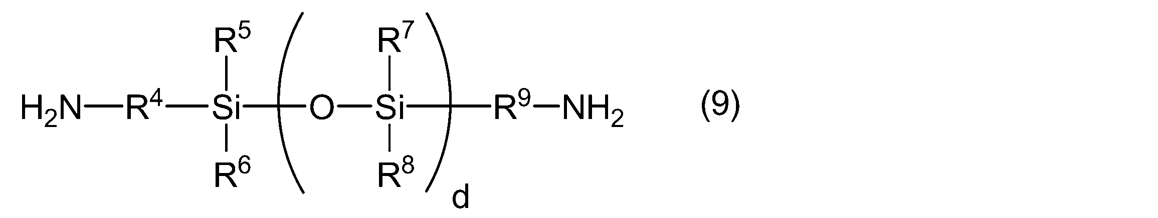

式 残存揮発分(%)=[(M2-M1)/M1]×100
(工程1)半導体ウェハ8内に形成された半導体チップ(半導体素子)12の回路面18上にフィルム状接着剤(接着剤層)1を積層する工程(図13(a)及び(b))。
(工程2)半導体チップ12の回路面18上に設けられた接着剤層1を露光及び現像によってパターニングする工程(図13(c)及び図14(a))。
(工程3)半導体ウェハ8を回路面18とは反対側の面から研磨して半導体ウェハ8を薄くする工程(図14(b))。
(工程4)半導体ウェハ8をダイシングにより複数の半導体チップ12に切り分ける工程(図14(c)及び図16(a))。
(工程5)半導体チップ12をピックアップして半導体装置用の板状の支持部材(半導体素子搭載用支持部材)13にマウントする工程(図16(b)及び図17(a))。
(工程6)支持部材13にマウントされた半導体チップ12aの回路面18上でパターニングされた接着剤層1に2層目の半導体チップ12bを積層する工程(図17(b))。
(工程7)半導体チップ12a及び12bをそれぞれ外部接続端子と接続する工程(図18)。
(工程1)
図13(a)に示す半導体ウェハ8内には、ダイシングラインDによって区分された複数の半導体チップ12が形成されている。この半導体チップ12の回路面18側の面にフィルム状接着剤(接着剤層)1を積層する(図13(b))。接着剤層1を積層する方法としては、予めフィルム状に成形されたフィルム状接着剤を準備し、これを半導体ウェハ8に貼り付ける方法が簡便であるが、スピンコート法などを用いて液状の感光性接着剤組成物のワニスを半導体ウェハ8に塗布し、加熱乾燥する方法によってもよい。
接着剤層1は、露光及び現像によってパターニングされた後に被着体に対する接着性を有し、アルカリ現像が可能なネガ型の感光性接着剤である。より詳細には、接着剤層1を露光及び現像によってパターニングして形成されるレジストパターン(接着剤パターン)が、半導体チップや支持部材等の被着体に対する接着性を有している。例えば接着剤パターンに被着体を必要により加熱しながら圧着することにより、接着剤パターンと被着体とを接着することが可能である。
パターニングの後、半導体ウェハ8の接着剤層1とは反対側の面を研磨して、半導体ウェハ8を所定の厚さまで薄くする(図14(b))。研磨は、例えば、接着剤層1上に粘着フィルムを貼り付け、粘着フィルムによって半導体ウェハ8を研磨用の治具に固定して行う。
研磨後、半導体ウェハ8の接着剤層1とは反対側の面に、ダイボンディング材30及びダイシングテープ40を有しこれらが積層している複合フィルム5を、ダイボンディング材30が半導体ウェハ8に接する向きで貼り付ける。貼り付けは必要により加熱しながら行う。
ダイシングの後、切り分けられた半導体チップ12を、接着剤層1及びダイボンディング材30とともにピックアップし(図16(b))、支持部材13にダイボンディング材30を介してマウントする(図17(a))。
支持部材13にマウントされた半導体チップ12a上の接着剤層1上に、2層目の半導体チップ12bを積層する(図17(b))。すなわち、半導体チップ12aと、その上層に位置する半導体チップ12bとが、それらの間に介在するパターニングされた接着剤層1(バッファーコート膜)によって接着される。半導体チップ12bは、パターニングされた接着剤層1のうち開口11は塞がないような位置に接着される。なお、半導体チップ12bの回路面18上にもパターニングされた接着剤層1(バッファーコート膜)が形成されている。
その後、半導体チップ12aはそのボンディングパッドに接続されたワイヤ14aを介して支持部材13上の外部接続端子と接続され、半導体チップ12bはそのボンディングパッドに接続されたワイヤ14bを介して支持部材13上の外部接続端子と接続される。次いで、半導体チップ12a及び12bを含む積層体を封止材15によって封止することにより、半導体装置200が得られる(図18)。
(第1工程)接続端子を有する支持部材13上に接着剤層1を設ける工程(図21及び図22)。
(第2工程)接着剤層1を露光及び現像により、接続端子が露出する開口11が形成されるようにパターニングする工程(図23及び図24)。
(第3工程)開口11に導電材を充填して導電層9を形成する工程(図25)。
(第4工程)接続用電極部を有する半導体チップ12を、支持部材13と接着剤層1との積層体の接着剤層1側に接着すると共に、支持部材13の接続端子と半導体チップ12の接続用電極部とを導電層9を介して電気的に接続する工程(図20)。
(第1工程)
図21に示す支持部材13の回路面18上に、接着剤層1を積層する(図22)。積層方法としては、予めフィルム状に成形されたフィルム状接着剤を準備し、これを支持部材13に貼り付ける方法が簡便であるが、スピンコート法などを用いて、感光性接着剤組成物を含有する液状のワニスを支持部材13上に塗布し、加熱乾燥する方法によって積層してもよい。
支持部材13上に設けられた接着剤層1に対して、所定の位置に開口が形成されているマスク4を介して活性光線(典型的には紫外線)を照射する(図23)。これにより接着剤層1が所定のパターンで露光される。
得られたレジストパターンの開口11に導電材を充填して導電層9を形成する(図25)。導電材の充填方法は、グラビア印刷、ロールによる押し込み、減圧充填等各種の方法が採用できる。ここで使用する導電材は、半田、金、銀、ニッケル、銅、白金、パラジウム若しくは酸化ルテニウム等の金属、又は、金属酸化物等からなる電極材料、上記金属のバンプの他、例えば、導電性粒子と樹脂成分とを少なくとも含有してなるものが挙げられる。導電性粒子としては、例えば、金、銀、ニッケル、銅、白金、パラジウム若しくは酸化ルテニウム等の金属若しくは金属酸化物、又は有機金属化合物等の導電性粒子が用いられる。また、樹脂成分としては、例えば、エポキシ樹脂及びその硬化剤等の上述した硬化性樹脂組成物が用いられる
支持部材13上の接着剤層1に対して、半導体チップ12が直接接着される。半導体チップ12の接続用電極部は、導電層9を介して支持部材13の接続端子と電気的に接続される。なお、半導体チップ12における接着剤層1と反対側の回路面上に、パターン化された接着剤層(バッファーコート膜)が形成されていてもよい。
(工程1)互いに対向する表面(第1の主面)7a及び裏面(第2の主面)7bを有するガラス基板7の表面7a上に本発明の感光性接着剤組成物からなる接着剤層1を設ける工程(図27及び図28)。
(工程2)裏面7b側から光を照射して接着剤層1を露光し、現像により接着層1をパターニングする工程(図29~図31)。
(工程3)パターニングされた接着剤層1に半導体素子12をその回路面がガラス基板7側に向くように直接接着する工程(図32)。
(工程4)互いに接着されたガラス基板7と半導体素子12とをダイシングして複数の半導体装置200に切り分ける工程(図33)。
(工程1)
図27に示されるガラス基板7の表面7a上に、本発明の感光性接着剤組成物からなる接着剤層1が設けられる(図28)。本実施形態においては、予め本発明の感光性接着剤組成物をフィルム状に成形してなるフィルム状接着剤を準備し、これをガラス基板7に貼り付ける方法が簡便である。
ガラス基板7の表面7a上に設けられた接着剤層1に対して、所定の位置に開口が形成されているマスク4をガラス基板7の裏面7b上に配置し、マスク4を介して裏面7b側から活性光線(典型的には紫外線)を照射する(図29)。これにより、活性光線はガラス基板7を透過して接着剤層1に照射され、接着剤層1は光硬化が進行して所定のパターンで露光される。
半導体素子12の回路面上に設けられた複数の有効画素領域17が、略正方形の辺に沿ったパターンに形成された接着層1にそれぞれ囲まれ、半導体素子12の回路面がガラス基板7側に向くように、半導体素子12が接着剤層1に直接接着される(図32)。接着剤層1は、半導体素子12を接着すると共に、有効画素領域17を囲む空間を確保するためのスペーサとしても機能している。半導体素子12の接着は、例えば、接着剤層1が流動性を発現するような温度にまで加熱しながら熱圧着する方法により行われる。熱圧着後、必要により接着剤層1を加熱して更に硬化を進行させる。
<(A)成分:ポリイミド樹脂>
(PI-1)
撹拌機、温度計及び窒素置換装置(窒素流入管)を備えたフラスコ内に、ジアミンである3,5-ジアミノ安息香酸(分子量152.2)(以下「DABA」と略す。)1.89g、脂肪族エーテルジアミン(BASF社製「D-400」(商品名)、分子量452.4)15.21g、及び1,1,3,3-テトラメチル-1,3-ビス(4-アミノフェニル)ジシロキサン(信越化学社製「LP-7100」(商品名)、分子量248.5)0.39gと、溶媒であるNMP(N-メチル-2-ピロリドン)116gを仕込み、撹拌してジアミンを溶媒に溶解させた。
撹拌機、温度計及び窒素置換装置(窒素流入管)を備えたフラスコ内に、ジアミンである2,2-ビス(4-(4-アミノフェノキシ)フェニル)プロパン(分子量410.5)(以下「BAPP」と略す。)20.5gと、溶媒であるNMP101gを仕込み、撹拌してジアミンを溶媒に溶解させた。
上記で得られたポリイミド樹脂(PI-1)及び(PI-2)を用いて、下記表1及び表2に示す組成比(単位:質量部)にて各成分を配合し、実施例1~7及び比較例1~3の感光性接着剤組成物(接着剤層形成用ワニス)を得た。
EA-5222:新中村化学工業社製、重合官能基当量380g/eq、エトキシ化ビスフェノールAジエポキシアクリレート
BPE-100:新中村化学工業社製、重合官能基当量240g/eq、エトキシ化ビスフェノールAジメタクリレート
BPE-500:新中村化学工業社製、重合官能基当量565g/eq、エトキシ化ビスフェノールAジメタクリレート
A―9300:新中村化学工業社製、重合官能基当量140g/eq、イソシアヌル酸EO変性トリアクリレート
UA-3110:新中村化学工業社製、重合官能基当量350g/eq、イソシアヌル酸変性トリアクリレート
UA-3330:新中村化学工業社製、重合官能基当量310g/eq、イソシアヌル酸変性トリアクリレート UF-8001G:共栄社化学社製、重合官能基当量2250g/eq、2官能ウレタンアクリレート
A―DPH:新中村化学工業社製、プロポキシ化ジペンタエリスリトールヘキサアクリレート、重合官能基当量95g/eq、6官能脂肪族系アクリレート
VG-3101:プリンテック、3官能エポキシ樹脂
YDF-8170C:東都化成社製、ビスフェノールFビスグリシジルエーテル
TrisP-PA:本州化学社製、トリスフェノール化合物(α,α,α´-トリス(4-ヒドロキシフェノル)-1-エチル-4-イソプロピルベンゼン)
R972:日本アエロジル社製、疎水性フュームドシリカ(平均粒径:約16nm)
I-819:チバ・スペシャルティ・ケミカルズ社製、ビス(2,4,6-トリメチルベンゾイル)-フェニルフォスフィンオキサイド
NMP:関東化学社製、N-メチル-2-ピロリドン


得られた実施例1~7及び比較例1~3の感光性接着剤組成物を、乾燥後の膜厚が50μmとなるように、それぞれ基材(剥離剤処理PETフィルム)上に塗布し、オーブン中にて80℃で20分間加熱し、続いて120℃で20分間加熱して、基材上に感光性接着剤組成物からなる接着剤層を形成した。このようにして、基材及び基材上に形成された接着剤層を有する接着シートを得た。実施例1~7及び比較例1~3の感光性接着剤組成物から得られた接着シートを、それぞれ、実施例1~7及び比較例1~3の接着シートとした。
(最低溶融粘度)
得られた実施例1~7及び比較例1~3の接着シートを、テフロンシート上に、ロール加圧(線圧4kgf/cm、送り速度0.5m/分)によって、接着剤層がテフロンシートと接するように積層(ラミネート)した。ロール加圧の温度条件は、実施例1~7及び比較例1~2の接着シートについては50℃とし、比較例3の接着シートについては150℃とした。このようにして、テフロンシート、接着剤層及び基材からなり、これらがこの順に積層する積層体を得た。
支持台上にシリコンウェハ(6インチ径、厚さ400μm)を載せ、その上に、上記接着シートを、接着剤層がシリコンウェハの裏面(支持台と反対側の面)と接するように、ロール加圧(温度100℃、線圧4kgf/cm、送り速度0.5m/分)により積層した。基材(PETフィルム)を剥離除去した後、露出した接着剤層上に、厚み80μm、幅10mm、長さ40mmのポリイミドフィルム(宇部興産社製、「ユーピレックス」(商品名))を、上記と同様の条件でロール加圧して積層した。このようにして、シリコンウェハ、接着剤層及びポリイミドフィルムからなり、これらがこの順に積層する積層体のサンプルを得た。
ロール加圧の温度を、実施例1~7及び比較例1~2の接着シートについては50℃、比較例3の接着シートについては150℃としたこと以外は、上記低温貼付性の評価試験と同様にして、シリコンウェハ上に接着シートを積層した。得られた積層体を、接着シート側から、高精度平行露光機(オーク製作所製、「EXM-1172-B-∞」(商品名))により1000mJ/cm2で露光し、80℃のホットプレート上で約30秒間放置した。基材(PETフィルム)を剥離除去した後、コンベア現像機(ヤコー社製)を用いて、テトラメチルアンモニウムハイドライド(TMAH)2.38質量%溶液を現像液とし、温度26℃、スプレー圧0.18MPaの条件でスプレー現像した後、温度25℃の純水にてスプレー圧0.02MPaの条件で6分間水洗し、150℃で1分間乾燥させた。このようにして、シリコンウェハ上に、感光性接着剤組成物からなる接着剤層を形成した。
ロール加圧の温度を、実施例1~7及び比較例1~2の接着シートについては60℃、比較例3の接着シートについては150℃としたこと以外は、上記高温接着性の評価試験と同様にして、シリコンウェハ上に接着シートを積層した。得られた積層体を、接着シート側から、ネガ型パターン用マスク(日立化成社製、「No.G-2」(商品名))を介して、上記試験と同様に露光した。次いで、上記試験と同様に、ホットプレート上で放置後、基材を除去し、現像・水洗を行った。このようにして、シリコンウェハ上に、感光性接着剤組成物からなる接着剤パターンを形成した。
ロール加圧の温度を、実施例1~7及び比較例1~2の接着シートについては50℃、比較例3の接着シートについては150℃とし、上記ネガ型パターン用マスクに代えて額縁状6インチサイズマスクパターン(中空部2mm、線幅0.5mm)を用いたこと以外は、上記パターン形成性の評価試験と同様にして、シリコンウェハ上に、感光性接着剤組成物からなる接着剤パターンを形成した。
シリコンウェハの厚さを280μmとし、ロール加圧の温度を50℃としたこと以外は、上記低温貼付性の評価試験と同様にして、シリコンウェハ上に接着シートを積層した。得られた積層体を、接着シート側から、高精度平行露光機(オーク製作所製、「EXM-1172-B-∞」(商品名))により1000mJ/cm2で露光し、80℃のホットプレート上で約30秒間放置後、15mm×40mmの大きさに個片化した。基材(PETフィルム)を剥がし、オーブン中で180℃、3時間の条件で加熱硬化することにより、シリコンウェハと、感光性接着剤組成物の硬化物からなる硬化物層からなる積層体が得られる。
<(A)成分:ポリイミド樹脂>
(PI-1)
撹拌機、温度計及び窒素置換装置(窒素流入管)を備えたフラスコ内に、ジアミンである3,5-ジアミノ安息香酸(分子量152.2)(以下「DABA」と略す。)1.89g、脂肪族エーテルジアミン(BASF社製「D-400」(商品名)、分子量452.4)15.21g、及び1,1,3,3-テトラメチル-1,3-ビス(4-アミノフェニル)ジシロキサン(信越化学社製「LP-7100」(商品名)、分子量248.5)0.39gと、溶媒であるNMP(N-メチル-2-ピロリドン)116gを仕込み、撹拌してジアミンを溶媒に溶解させた。
撹拌機、温度計及び窒素置換装置(窒素流入管)を備えたフラスコ内に、ジアミンである2,2-ビス(4-(4-アミノフェノキシ)フェニル)プロパン(分子量410.5)(以下「BAPP」と略す。)20.5gと、溶媒であるNMP101gを仕込み、撹拌してジアミンを溶媒に溶解させた。
(C-1)
撹拌機、温度計及び窒素置換装置(窒素流入管)を備えた500mLフラスコ内に、液状の高純度ビスフェノールAビスグリシジルエーテルエポキシ樹脂(エポキシ当量178g/eq)178g(1.0当量)、アクリル酸36g(0.5当量)、トリフェニルホスフィン0.5g、及びヒドロキノン0.15gを仕込み、100℃で7時間反応させることにより、エポキシ基を有する単官能(メタ)アクリレートである放射線重合性化合物(C-1)を得た。(C-1)は、エチレン性不飽和基及びエポキシ基を有する反応性化合物である。(C-1)の酸価は0.3KOHmg/g以下であり、5%重量減少温度は300℃であった。なお、酸価は水酸化カリウムのエタノール溶液で滴定することにより求め、5%重量減少温度は、示差熱熱重量同時測定装置(エスアイアイ・ナノテクノロジー社製、「TG/DTA 6300」(商品名))を用いて、窒素フロー:400ml/minの条件下で測定した。(C-1)のエポキシ基数は約1、エチレン性不飽和基数は約1、放射線重合性官能基当量は410g/eqであり、全塩素含量は400ppm以下であった。
エポキシ樹脂として、液状の高純度ビスフェノールFビスグリシジルエーテルエポキシ樹脂(エポキシ当量160g/eq)168g(1.0当量)を用いたこと以外は(C-1)と同様にして、(C-2)を得た。(C-2)の酸価は0.3KOHmg/g以下であり、5%重量減少温度は300℃であった。(C-2)のエポキシ基数は約1、エチレン性不飽和基数は約1、放射線重合性官能基当量は395g/eqであり、全塩素含量は400ppm以下であった。
上記で得られたポリイミド樹脂(PI-1)及び(PI-2)並びに放射線重合性化合物(C-1)及び(C-2)を用いて、下記表3及び表4に示す組成比(単位:質量部)にて各成分を配合し、実施例I~V及び比較例I~IIの感光性接着剤組成物(接着剤層形成用ワニス)を得た。
BPE-100:新中村化学工業社製、エトキシ化ビスフェノールAジメタクリレート(放射線重合性官能基当量240g/eq、5%重量減少温度:330℃)
A-9300:新中村化学工業社製、イソシアヌル酸EO変性トリアクリレート(放射線重合性官能基当量140g/eq、5%重量減少温度:>400℃)
M-140:東亜合成社製、2-(1,2-シクロヘキサカルボキシイミド)エチルアクリレート(放射線重合性官能基当量251g/eq、5%重量減少温度:200℃、グリシジル基数:0、アクリル基数:1)
4-HBAGE:日本化成社製、4-ヒドロキシブチルアクリレートグリシジルエーテル(放射線重合性官能基当量200g/eq、5%重量減少温度:135℃)
VG-3101:プリンテック(株)製、3官能エポキシ樹脂(5%重量減少温度:350℃)
YDF-870GS:東都化成社製、ビスフェノールFビスグリシジルエーテル(5%重量減少温度:270℃)
TrisP-PA:本州化学社製、トリスフェノール化合物(α,α,α’-トリス(4-ヒドロキシフェノル)-1-エチル-4-イソプロピルベンゼン)(5%重量減少温度:350℃)
R-972:日本アエロジル社製、疎水性フュームドシリカ(平均粒径:約16nm)
I-819:チバ・スペシャルティ・ケミカルズ社製、ビス(2,4,6-トリメチルベンゾイル)-フェニルフォスフィンオキサイド
パークミルD:日油社製、ジクミルパーオキサイド(1分間半減期温度:175℃)
NMP:関東化学社製、N-メチル-2-ピロリドン

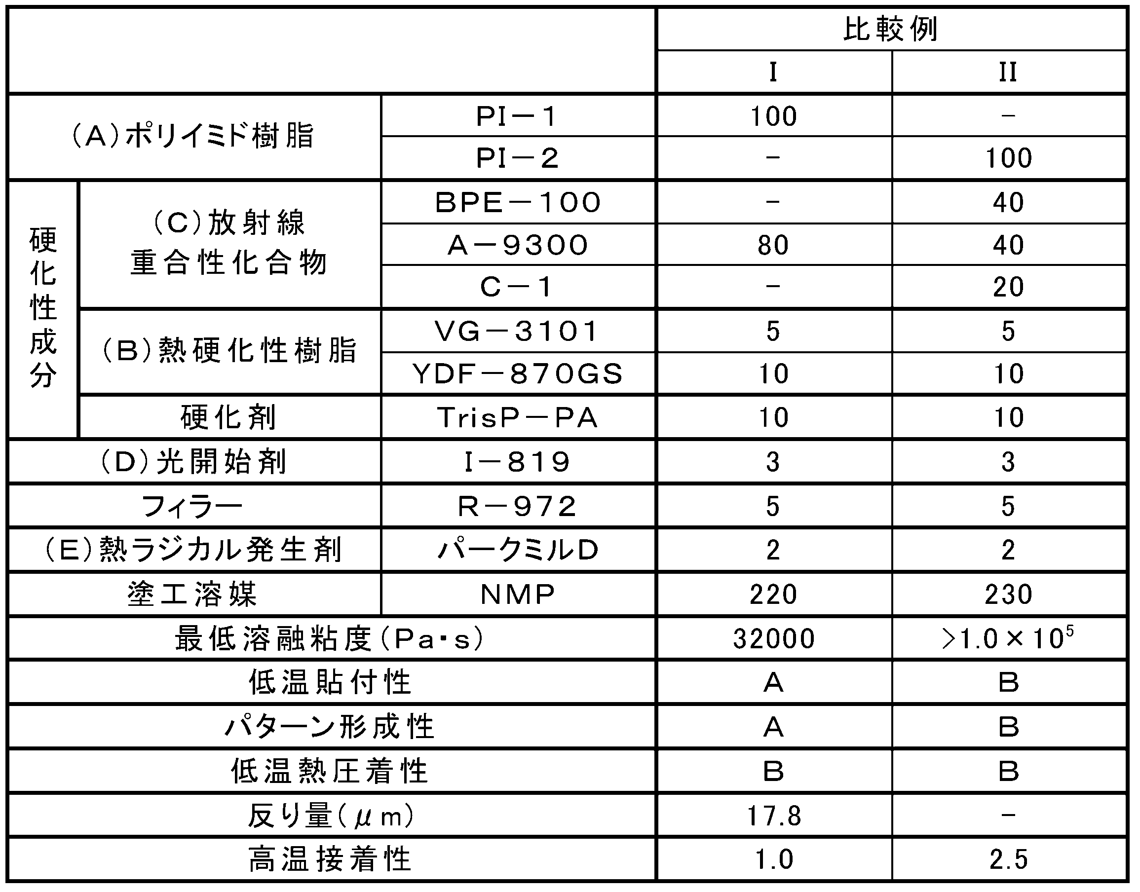
得られた実施例I~V及び比較例I~IIの感光性接着剤組成物を、乾燥後の膜厚が50μmとなるように、それぞれ基材(剥離剤処理PETフィルム)上に塗布し、オーブン中にて80℃で20分間加熱し、続いて120℃で20分間加熱して、基材上に感光性接着剤組成物からなる接着剤層を形成した。このようにして、基材及び基材上に形成された接着剤層を有する接着シートを得た。実施例I~V及び比較例I~IIの感光性接着剤組成物から得られた接着シートを、それぞれ、実施例I~V及び比較例I~IIの接着シートとした。
(最低溶融粘度)
得られた実施例I~V及び比較例I~IIの接着シートを、テフロンシート上に、ロール加圧(温度50℃、線圧4kgf/cm、送り速度0.5m/分)によって、接着剤層がテフロンシートと接するように積層(ラミネート)した。このようにして、テフロンシート、接着剤層及び基材からなり、これらがこの順に積層する積層体を得た。
支持台上にシリコンウェハ(6インチ径、厚さ400μm)を載せ、その上に、上記接着シートを、接着剤層がシリコンウェハの裏面(支持台と反対側の面)と接するように、ロール加圧(温度100℃、線圧4kgf/cm、送り速度0.5m/分)により積層した。基材(PETフィルム)を剥離除去した後、露出した接着剤層上に、厚み80μm、幅10mm、長さ40mmのポリイミドフィルム(宇部興産社製、「ユーピレックス」(商品名))を、上記と同様の条件でロール加圧して積層した。このようにして、シリコンウェハ、接着剤層及びポリイミドフィルムからなり、これらがこの順に積層する積層体のサンプルを得た。
ロール加圧の温度を、実施例I~V及び比較例Iの接着シートについては50℃、比較例IIの接着シートについては150℃としたこと以外は、上記低温貼付性の評価試験と同様にして、シリコンウェハ上に接着シートを積層した。得られた積層体を、接着シート側から、高精度平行露光機(オーク製作所製、「EXM-1172-B-∞」(商品名))により1000mJ/cm2で露光し、80℃のホットプレート上で約30秒間放置した。基材(PETフィルム)を剥離除去した後、コンベア現像機(ヤコー社製)を用いて、テトラメチルアンモニウムハイドライド(TMAH)2.38質量%溶液を現像液とし、温度26℃、スプレー圧0.18MPaの条件でスプレー現像した後、温度25℃の純水にてスプレー圧0.02MPaの条件で6分間水洗し、150℃で1分間乾燥させた。このようにして、シリコンウェハ上に、感光性接着剤組成物からなる接着剤層を形成した。
ロール加圧の温度を、実施例I~V及び比較例Iの接着シートについては60℃、比較例IIの接着シートについては150℃としたこと以外は、上記高温接着性の評価試験と同様にして、シリコンウェハ上に接着シートを積層した。得られた積層体を、接着シート側から、ネガ型パターン用マスク(日立化成社製、「No.G-2」(商品名))を介して、上記試験と同様に露光した。次いで、上記試験と同様に、ホットプレート上で放置後、基材を除去し、現像・水洗を行った。このようにして、シリコンウェハ上に、感光性接着剤組成物からなる接着剤パターンを形成した。
ロール加圧の温度を、実施例I~V及び比較例Iの接着シートについては50℃、比較例IIの接着シートについては150℃とし、上記ネガ型パターン用マスクに代えて額縁状6インチサイズマスクパターン(中空部2mm、線幅0.5mm)を用いたこと以外は、上記パターン形成性の評価試験と同様にして、シリコンウェハ上に、感光性接着剤組成物からなる接着剤パターンを形成した。
<(A)成分:熱可塑性樹脂>
ポリイミド樹脂
(PI-3)
撹拌機、温度計及び窒素置換装置(窒素流入管)を備えた300mLフラスコ内に、ジアミンである5,5´-メチレンビス(アントラニル酸)(分子量286.3)(以下「MBAA」と略す。)2.16g(0.0075mol)、ポリオキシプロピレンジアミン(商品名「D-400」(分子量:452.4)、BASF製製)15.13g(0.0335mol)、及び1,1,3,3-テトラメチル-1,3-ビス(3-アミノプロピル)ジシロキサン(商品名「BY16-871EG」、東レ・ダウコーニング(株)製)1.63g(0.0065mol)と、溶媒であるNMP(N-メチル-2-ピロリドン)115gを仕込み、撹拌してジアミンを溶媒に溶解させた。
撹拌機、温度計及び窒素置換装置を備えたフラスコ内に、ジアミンであるMBAA5.72g(0.02mol)、「D-400」13.57g(0.03mol)、「BY16-871EG」2.48g(0.01mol)、及び1,4-ブタンジオール ビス(3-アミノプロピル)エーテル(商品名「B-12」、東京化成製、分子量204.31)8.17g(0.04mol)と、溶媒であるNMP110gを仕込み、撹拌してジアミンを溶媒に溶解させた。
撹拌機、温度計及び窒素置換装置を備えた500mLフラスコ内に、ジアミンであるMBAA34.32g(0.12mol)、「D-400」17.32g(0.04mol)、及び「BY16-871EG」7.454g(0.03mol)と、溶媒であるNMP140gを仕込み、撹拌してジアミンを溶媒に溶解させた。
(Polymer―1)
プロピレングリコールモノメチルエーテルアセテート240g、乳酸メチル60g、メタクリロイルオキシトリシクロ[5.2.1.02,6]デカン(日立化成工業(株)社製、「FANCRYL FA-513M」)86.4g、N-シクロヘキシルマレイミド36.5g、2-ヒドロキシエチルメタクリレート106.7g、及びメタクリル酸40.5gを混合し、窒素バブリングしながら溶解させた。N-シクロヘキシルマレイミドの溶解を確認した後、2,2’-アゾビスイソブチロニトリル3gを溶解させ、混合溶液(a)を調製した。
(C-1)
撹拌機、温度計及び窒素置換装置(窒素流入管)を備えた500mLフラスコ内に、液状の高純度ビスフェノールAビスグリシジルエーテルエポキシ樹脂(エポキシ当量178g/eq)178g(1.0当量)、アクリル酸36g(0.5当量)、トリフェニルホスフィン0.5g、及びヒドロキノン0.15gを仕込み、100℃で7時間反応させることにより、エポキシ基を有する単官能(メタ)アクリレートである放射線重合性化合物(C-1)を得た。(C-1)は、エチレン性不飽和基及びエポキシ基を有する反応性化合物である。(C-1)の酸価は0.3KOHmg/g以下であり、5%重量減少温度は300℃であった。なお、酸価は水酸化カリウムのエタノール溶液で滴定することにより求め、5%重量減少温度は、示差熱熱重量同時測定装置(エスアイアイ・ナノテクノロジー社製、「TG/DTA 6300」(商品名))を用いて、窒素フロー:400ml/minの条件下で測定した。(C-1)のエポキシ基数は約1、エチレン性不飽和基数は約1、放射線重合性官能基当量410g/eqであり、全塩素含量は400ppm以下であった。
エポキシ樹脂として、液状の高純度ビスフェノールFビスグリシジルエーテルエポキシ樹脂(エポキシ当量160g/eq)168g(1.0当量)を用いたこと以外は(C-1)と同様にして、(C-2)を得た。(C-2)の酸価は0.3KOHmg/g以下であり、5%重量減少温度は300℃であった。(C-2)のエポキシ基数は約1、エチレン性不飽和基数は約1、放射線重合性官能基当量395g/eqであり、全塩素含量は400ppm以下であった。
撹拌機、温度計及び窒素置換装置を備えた500mLフラスコ内に、フェノールノボラック型エポキシ樹脂(エポキシ当量174g/eq、東都化成社製「YDPN-638」)174g(1.0当量)、アクリル酸36g(0.5当量)、トリフェニルホスフィン0.48g、及びヒドロキノン0.10gを仕込み、90℃~100℃で7時間反応させることにより、エポキシ基を有する単官能(メタ)アクリレートである放射線重合性化合物(C-3)を得た。(C-3)は、エチレン性不飽和基及びエポキシ基を有する反応性化合物である。(C-3)の酸価は0.3KOHmg/g以下であり、5%重量減少温度は310℃であった。なお、酸価は水酸化カリウムのエタノール溶液で滴定することにより求め、5%重量減少温度は、示差熱熱重量同時測定装置(エスアイアイ・ナノテクノロジー社製、「TG/DTA 6300」(商品名))を用いて、窒素フロー:400ml/minの条件下で測定した。(C-3)のエポキシ基数は約1.7、エチレン性不飽和基数は約1.7、放射線重合性官能基当量440g/eqであり、全塩素含量は400ppm以下であった。
上記で得られたポリイミド樹脂(PI-3)~(PI-5)及び放射線重合性化合物(C-1)~(C-3)を用いて、下記表5及び表6に示す組成比(単位:質量部)にて各成分を配合し、実施例i~viii及び比較例i~viiの感光性接着剤組成物(接着剤層形成用ワニス)を得た。
BPE-100:新中村化学工業社製、エトキシ化ビスフェノールAジメタクリレート(放射線重合性官能基当量240g/eq、5%重量減少温度:330℃)
A-9300:新中村化学工業社製、イソシアヌル酸EO変性トリアクリレート(放射線重合性官能基当量140g/eq、5%重量減少温度:>400℃)
EA-1020:新中村化学工業社製、ビスフェノールAビスグリシジルエーテル型ジアクリレート(放射線重合性官能基当量228g/eq、5%重量減少温度:300℃)
M-140:東亜合成社製、2-(1,2-シクロヘキサカルボキシイミド)エチルアクリレート(放射線重合性官能基当量251g/eq、5%重量減少温度:200℃、グリシジル基数:0、アクリル基数:1)
VG-3101:プリンテック(株)製、3官能エポキシ樹脂(5%重量減少温度:350℃)
YDF-870GS:東都化成社製、ビスフェノールFビスグリシジルエーテル(5%重量減少温度:270℃)
TrisP-PA:本州化学社製、トリスフェノール化合物(α,α,α’-トリス(4-ヒドロキシフェノル)-1-エチル-4-イソプロピルベンゼン)(5%重量減少温度:350℃)
HRM-2019:昭和高分子社製、フェノール性水酸基含有アクリレート(5%重量減少温度:210℃、フェノール性水酸基数:約4、アクリル基数:約4)
R-972:日本アエロジル社製、疎水性フュームドシリカ(平均粒径:約16nm)
I-819:チバ・スペシャルティ・ケミカルズ社製、ビス(2,4,6-トリメチルベンゾイル)-フェニルフォスフィンオキサイド
パークミルD:日油社製、ジクミルパーオキサイド(1分間半減期温度:175℃)
NMP:関東化学社製、N-メチル-2-ピロリドン
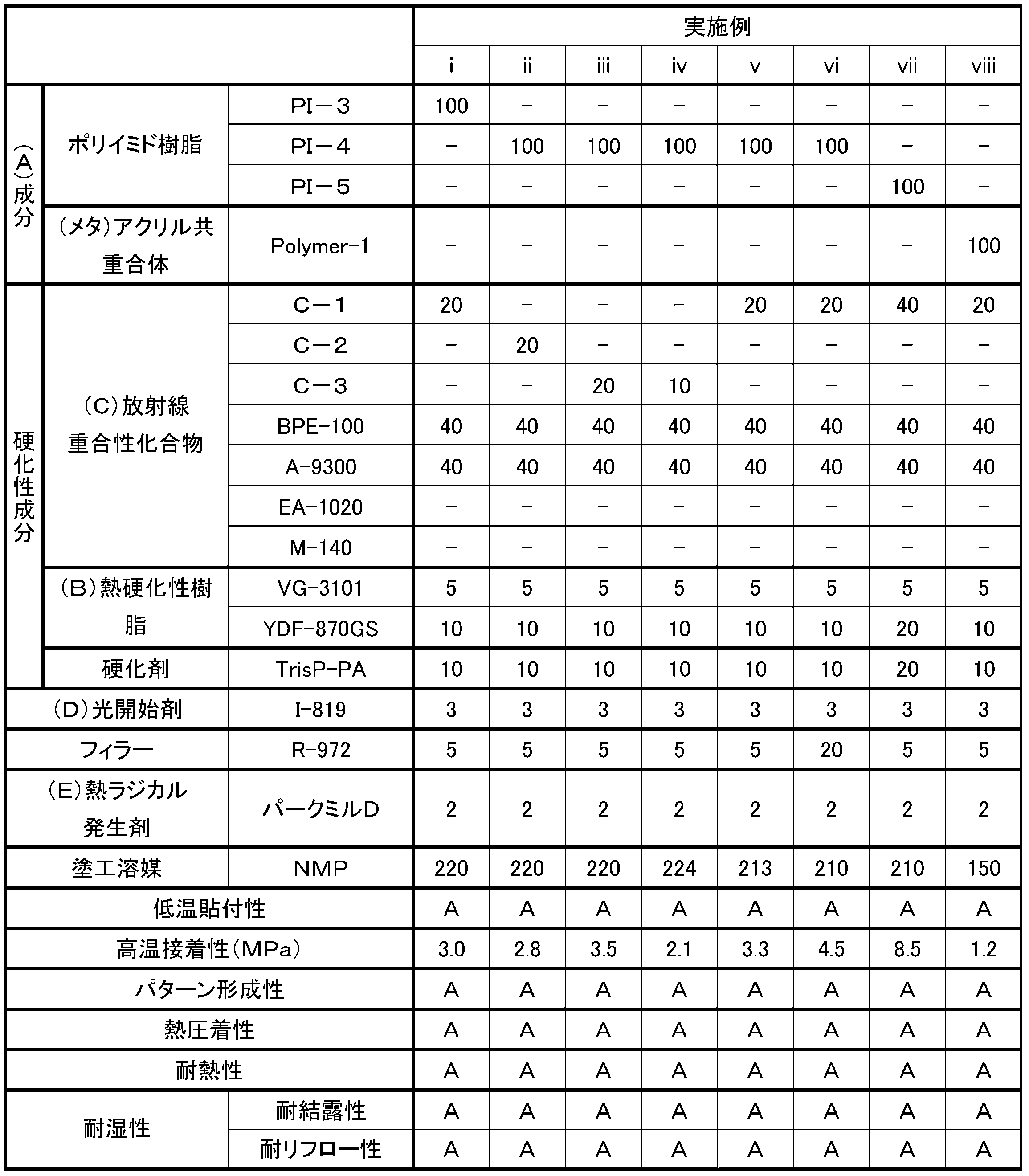

サンプルを示差熱熱重量同時測定装置(エスアイアイ・ナノテクノロジー社製、商品名「TG/DTA6300」)を用いて、昇温速度10℃/min、窒素フロー(400ml/分)下で5%重量減少温度を測定した。
全塩素含量はJIS K7243-3に準じて測定した。
得られた実施例i~viii及び比較例i~viiの感光性接着剤組成物を、乾燥後の膜厚が50μmとなるように、それぞれ基材(剥離剤処理PETフィルム)上に塗布し、オーブン中にて80℃で20分間加熱し、続いて120℃で20分間加熱して、基材上に感光性接着剤組成物からなる接着剤層を形成した。このようにして、基材及び基材上に形成された接着剤層を有する接着シートを得た。実施例i~viii及び比較例i~viiの感光性接着剤組成物から得られた接着シートを、それぞれ、実施例i~viii及び比較例i~viiの接着シートとした。
実施例I~V及び比較例I~IIと同様に、低温貼付性の評価を行った。評価結果を表5及び表6に示す。
ロール加圧の温度を80℃としたこと以外は、上記低温貼付性の評価試験と同様にして、シリコンウェハ上に接着シートを積層した。得られた積層体を、接着シート側から、高精度平行露光機(オーク製作所製、「EXM-1172-B-∞」(商品名))により1000mJ/cm2で露光し、80℃のホットプレート上で約30秒間放置した。基材(PETフィルム)を剥離除去した後、コンベア現像機(ヤコー社製)を用いて、テトラメチルアンモニウムハイドライド(TMAH)2.38質量%溶液を現像液とし、温度26℃、スプレー圧0.18MPaの条件でスプレー現像した後、温度25℃の純水にてスプレー圧0.02MPaの条件で6分間水洗し、150℃で1分間乾燥させた。このようにして、シリコンウェハ上に、感光性接着剤組成物からなる接着剤層を形成した。
ロール加圧の温度を80℃としたこと以外は、実施例I~V及び比較例I~IIと同様に、パターン形成性の評価を行った。評価結果を表5及び表6に示す。
上記ネガ型パターン用マスクに代えて額縁状6インチサイズマスクパターン(中空部2mm、線幅0.5mm)を用いたこと以外は、上記パターン形成性の評価試験と同様にして、シリコンウェハ上に、感光性接着剤組成物からなる接着剤パターンを形成した。
上記低温熱圧着性の評価試験と同様にして、シリコンウェハ、接着剤パターン及びガラス基板からなり、これらがこの順に積層する積層体のサンプルを得た。得られたサンプルを、オーブン中で180℃、3時間の条件で加熱し、さらに、260℃のホットプレート上に30分間静置した。その後、サンプルを顕微鏡(倍率:50倍)にて観察し、1ICサイズ以上の剥離が見られなかったものをA、1ICサイズ以上の剥離が見られたものをBとして、耐熱性の評価を行った。評価結果を表5及び表6に示す。
上記耐熱性の評価試験と同様に、積層体のサンプルをオーブン中で180℃にて3時間加熱した。加熱後のサンプルを、温度85℃、湿度60%の条件下で168時間処理した後、温度25℃、湿度50%の環境に置き、サンプルのガラス内部が結露するか顕微鏡(倍率:50倍)で観察した。結露が見られなかったものをA、結露が見られたものをBとして、耐湿性(耐結露性)の評価を行った。評価結果を表5及び表6に示す。
<(A)成分:ポリイミド樹脂>
(PI-3)
撹拌機、温度計及び窒素置換装置(窒素流入管)を備えた300mLフラスコ内に、ジアミンである5,5´-メチレンビス(アントラニル酸)(分子量286.3)(以下「MBAA」と略す。)2.16g(0.0075mol)、ポリオキシプロピレンジアミン(商品名「D-400」(分子量:452.4)、BASF製製)15.13g(0.0335mol)、及び1,1,3,3-テトラメチル-1,3-ビス(3-アミノプロピル)ジシロキサン(商品名「BY16-871EG」、東レ・ダウコーニング(株)製)1.63g(0.0065mol)と、溶媒であるNMP(N-メチル-2-ピロリドン)115gを仕込み、撹拌してジアミンを溶媒に溶解させた。
撹拌機、温度計及び窒素置換装置を備えたフラスコ内に、ジアミンである2,2-ビス(4-(4-アミノフェノキシ)フェニル)プロパン(分子量410.5)(以下「BAPP」と略す。)20.5gと、溶媒であるNMP101gを仕込み、撹拌してジアミンを溶媒に溶解させた。
上記で得られたポリイミド樹脂(PI-3)及び(PI-6)を用いて、下記表7及び表8に示す組成比(単位:質量部)にて各成分を配合し、実施例a~e及び比較例a~eの感光性接着剤組成物(接着剤層形成用ワニス)を得た。
BPE-100:新中村化学工業社製、エトキシ化ビスフェノールAジメタクリレート(放射線重合性官能基当量240g/eq、5%重量減少温度:330℃)
BPE-500:新中村化学工業社製、エトキシ化ビスフェノールAジメタクリレート(放射線重合性官能基当量565g/eq、5%重量減少温度:330℃)
A-9300:新中村化学工業社製、イソシアヌル酸EO変性トリアクリレート(放射線重合性官能基当量140g/eq、5%重量減少温度:>400℃)
U-2PPA:新中村化学工業社製、2官能ウレタンアクリレート(放射線重合性官能基当量230g/eq、5%重量減少温度:160℃)
VG-3101:プリンテック(株)製、3官能エポキシ樹脂(5%重量減少温度:350℃)
YDF-870GS:東都化成社製、ビスフェノールFビスグリシジルエーテル(5%重量減少温度:270℃)
TrisP-PA:本州化学社製、トリスフェノール化合物(α,α,α’-トリス(4-ヒドロキシフェノル)-1-エチル-4-イソプロピルベンゼン)(5%重量減少温度:350℃)
R-972:日本アエロジル社製、疎水性フュームドシリカ(平均粒径:約16nm)
I-819:チバ・スペシャルティ・ケミカルズ社製、ビス(2,4,6-トリメチルベンゾイル)-フェニルフォスフィンオキサイド
パーヘキサ25B:日油社製、2,5-ジメチル-2,5-ジ(t-ブチルパーオキシへキサン)(1分間半減期温度:180℃)
パークミルD:日油社製、ジクミルパーオキサイド(1分間半減期温度:175℃)
パーロイルL:日油社製、ジラウロイルパーオキサイド(1分間半減期温度:116℃)
NMP:関東化学社製、N-メチル-2-ピロリドン
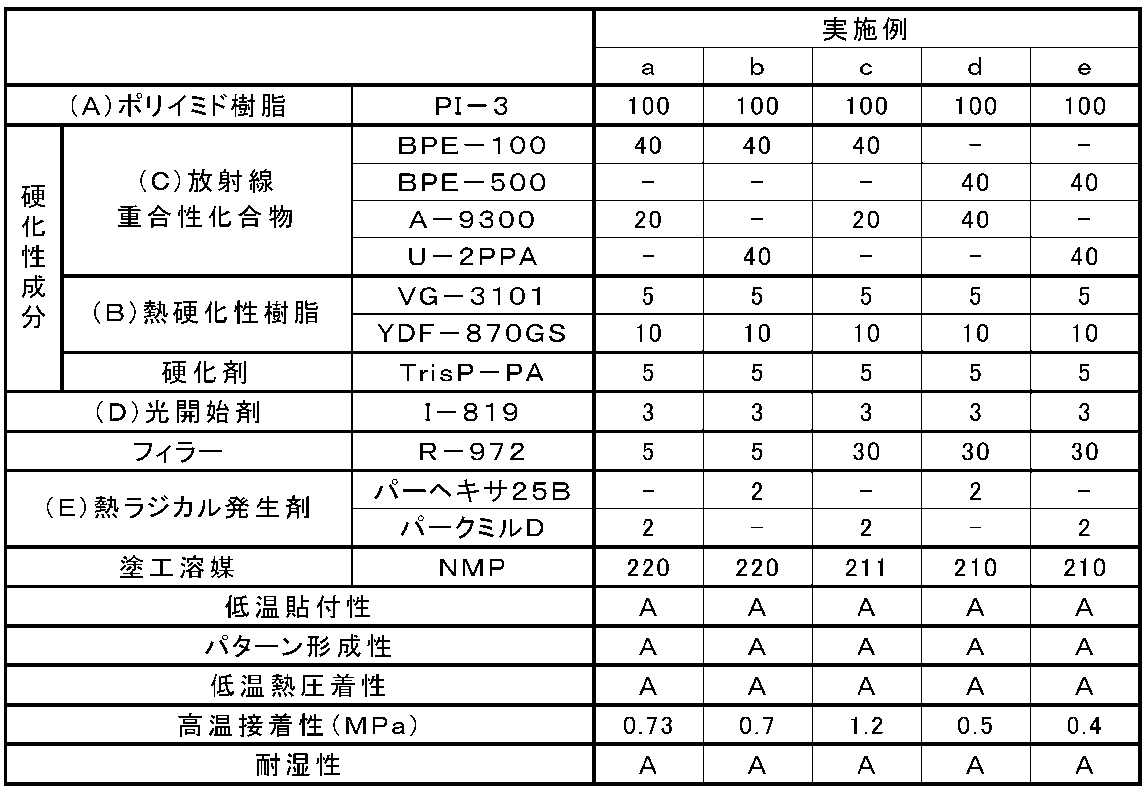

得られた実施例a~e及び比較例a~eの感光性接着剤組成物を、乾燥後の膜厚が50μmとなるように、それぞれ基材(剥離剤処理PETフィルム)上に塗布し、オーブン中にて80℃で20分間加熱し、続いて120℃で20分間加熱して、基材上に感光性接着剤組成物からなる接着剤層を形成した。このようにして、基材及び基材上に形成された接着剤層を有する接着シートを得た。実施例a~e及び比較例a~eの感光性接着剤組成物から得られた接着シートを、それぞれ、実施例a~e及び比較例a~eの接着シートとした。
実施例I~V及び比較例I~IIと同様に、低温貼付性の評価を行った。評価結果を表7及び表8に示す。
ロール加圧の温度を、実施例a~e及び比較例a~dについては50℃、比較例eについては200℃としたこと以外は、上記低温貼付性の評価試験と同様にして、シリコンウェハ上に接着シートを積層した。得られた積層体を、接着シート側から、高精度平行露光機(オーク製作所製、「EXM-1172-B-∞」(商品名))により1000mJ/cm2で露光し、80℃のホットプレート上で約30秒間放置した。基材(PETフィルム)を剥離除去した後、コンベア現像機(ヤコー社製)を用いて、テトラメチルアンモニウムハイドライド(TMAH)2.38質量%溶液を現像液とし、温度26℃、スプレー圧0.18MPaの条件でスプレー現像した後、温度25℃の純水にてスプレー圧0.02MPaの条件で6分間水洗し、150℃で1分間乾燥させた。このようにして、シリコンウェハ上に、感光性接着剤組成物からなる接着剤層を形成した。
ロール加圧の温度を50℃としたこと以外は、実施例I~V及び比較例I~IIと同様に低温熱圧着性の評価試験を行った。結果を表7及び表8に示す。
ロール加圧の温度を、実施例a~e及び比較例a~dについては100℃、比較例eについては200℃としたこと以外は実施例I~V及び比較例I~IIと同様にパターン形成性の評価試験を行った。結果を表7及び表8に示す。
上記高温接着性の評価試験と同様にして、シリコンウェハ上に接着シートを積層した。得られた積層体を、接着シート側から、額縁状6インチサイズマスクパターン(中空部2mm、線幅0.5mm)を介して、高精度平行露光機により500mJ/cm2で露光し、80℃のホットプレート上で約30秒間放置した。基材(PETフィルム)を剥離除去した後、コンベア現像機を用いて、TMAH2.38質量%水溶液を現像液とし、温度26℃、スプレー圧0.18MPaの条件でスプレー現像した後、温度25℃の純水にてスプレー圧0.02MPaの条件で6分間水洗した。接着剤層付きシリコンウェハを150℃で1分間乾燥させた後、ガラス基板(15mm×40mm×0.55mm)を、接着剤層をガラス基板側にして載せ、0.5MPaで加圧しながら、実施例a~e及び比較例a~dの接着シートは温度150℃で、比較例eの接着シートは温度300℃で10分間圧着した。こうして得られた試験片を、オーブン中で150℃、3時間の条件で加熱硬化した。
Claims (47)
- パターン形成後の20℃~200℃における最低溶融粘度が30000Pa・s以下である感光性接着剤組成物。
- (A)アルカリ可溶性樹脂、(B)熱硬化性樹脂、(C)放射線重合性化合物及び(D)光開始剤を含有する、請求項1に記載の感光性接着剤組成物。
- 前記(C)放射線重合性化合物の平均官能基当量が230g/eq以上である、請求項2に記載の感光性接着剤組成物。
- 前記(C)放射線重合性化合物が、ウレタン結合及び/又はイソシアヌル環を有する(メタ)アクリレートを含む、請求項2又は3に記載の感光性接着剤組成物。
- 前記(C)放射線重合性化合物が単官能(メタ)アクリレートを含む、請求項2に記載の感光性接着剤組成物。
- 前記単官能(メタ)アクリレートの5%重量減少温度が150℃以上である、請求項5に記載の感光性接着剤組成物。
- 前記単官能(メタ)アクリレートが、エポキシ基を有する単官能(メタ)アクリレートである、請求項6に記載の感光性接着剤組成物。
- 前記(B)熱硬化性樹脂がエポキシ樹脂を含む、請求項2~7のいずれか一項に記載の感光性接着剤組成物。
- 前記(A)アルカリ可溶性樹脂のTgが150℃以下である、請求項2~8のいずれか一項に記載の感光性接着剤組成物。
- 前記(A)アルカリ可溶性樹脂がカルボキシル基及び/又は水酸基を有する熱可塑性樹脂である、請求項2~9のいずれか一項に記載の感光性接着剤組成物。
- 前記(A)アルカリ可溶性樹脂がポリイミド樹脂である、請求項2~10のいずれか一項に記載の感光性接着剤組成物。
- (E)熱ラジカル発生剤を更に含有する、請求項2~11のいずれか一項に記載の感光性樹脂組成物。
- 前記(E)熱ラジカル発生剤が有機過酸化物である、請求項12に記載の感光性接着剤組成物。
- 請求項1~13のいずれか一項に記載の感光性接着剤組成物をフィルム状に成形することにより得られる、フィルム状接着剤。
- 基材と、該基材上に形成された請求項14に記載のフィルム状接着剤からなる接着剤層と、を備える接着シート。
- 被着体上に積層された請求項14に記載のフィルム状接着剤からなる接着剤層を、フォトマスクを介して露光し、露光後の前記接着剤層をアルカリ現像液により現像処理することにより得られる接着剤パターン。
- 半導体ウェハと、該半導体ウェハ上に積層された請求項14に記載のフィルム状接着剤からなる接着剤層と、を備える接着剤層付半導体ウェハ。
- 請求項1~13のいずれか一項に記載の感光性接着剤組成物を用いて、半導体素子同士、及び/又は、半導体素子と半導体素子搭載用支持部材とが接着された構造を有する半導体装置。
- 前記半導体素子搭載用支持部材が透明基板である、請求項18に記載の半導体装置。
- (A)アルカリ可溶性樹脂、(B)熱硬化性樹脂、(C)放射線重合性化合物及び(D)光開始剤を含有する感光性接着剤組成物であって、
前記(C)放射線重合性化合物の平均官能基当量が230g/eq以上である、感光性接着剤組成物。 - 前記(C)放射線重合性化合物が、ウレタン結合及び/又はイソシアヌル環を有する(メタ)アクリレートを含む、請求項20に記載の感光性接着剤組成物。
- 前記(B)熱硬化性樹脂がエポキシ樹脂を含む、請求項20又は21に記載の感光性接着剤組成物。
- 前記(A)アルカリ可溶性樹脂のTgが150℃以下である、請求項20~22のいずれか一項に記載の感光性接着剤組成物。
- 前記(A)アルカリ可溶性樹脂がカルボキシル基及び/又は水酸基を有する熱可塑性樹脂である、請求項20~23のいずれか一項に記載の感光性接着剤組成物。
- 前記(A)アルカリ可溶性樹脂がポリイミド樹脂である、請求項20~24のいずれか一項に記載の感光性接着剤組成物。
- 請求項20~25のいずれか一項に記載の感光性接着剤組成物をフィルム状に成形することにより得られる、フィルム状接着剤。
- 基材と、該基材上に形成された請求項26に記載のフィルム状接着剤からなる接着剤層と、を備える接着シート。
- 被着体上に積層された請求項26に記載のフィルム状接着剤からなる接着剤層を、フォトマスクを介して露光し、露光後の前記接着剤層をアルカリ現像液により現像処理することにより得られる接着剤パターン。
- 半導体ウェハと、該半導体ウェハ上に積層された請求項26に記載のフィルム状接着剤からなる接着剤層と、を備える接着剤層付半導体ウェハ。
- 請求項20~25のいずれか一項に記載の感光性接着剤組成物を用いて、半導体素子同士、及び/又は、半導体素子と半導体素子搭載用支持部材とが接着された構造を有する半導体装置。
- 前記半導体素子搭載用支持部材が透明基板である、請求項30に記載の半導体装置。
- (A)熱可塑性樹脂、(B)熱硬化性樹脂、(C)放射線重合性化合物及び(D)光開始剤を含有する感光性接着剤組成物であって、
前記(C)放射線重合性化合物がエチレン性不飽和基及びエポキシ基を有する化合物を含む、感光性接着剤組成物。 - 前記(A)熱可塑性樹脂がアルカリ可溶性樹脂である、請求項32に記載の感光性接着剤組成物。
- 前記エチレン性不飽和基及びエポキシ基を有する化合物の5%重量減少温度が150℃以上である、請求項32又は33に記載の感光性接着剤組成物。
- 前記エチレン性不飽和基及びエポキシ基を有する化合物がエポキシ基を有する単官能(メタ)アクリレートである、請求項32~34のいずれか一項に記載の感光性接着剤組成物。
- 前記(B)熱硬化性樹脂がエポキシ樹脂を含む、請求項32~35のいずれか一項に記載の感光性接着剤組成物。
- 前記アルカリ可溶性樹脂のTgが150℃以下である、請求項33~36のいずれか一項に記載の感光性接着剤組成物。
- 前記アルカリ可溶性樹脂がカルボキシル基及び/又は水酸基を有する熱可塑性樹脂である、請求項33~37のいずれか一項に記載の感光性接着剤組成物。
- 前記アルカリ可溶性樹脂がポリイミド樹脂である、請求項33~38のいずれか一項に記載の感光性接着剤組成物。
- (E)熱ラジカル発生剤を更に含有する、請求項32~39のいずれか一項に記載の感光性樹脂組成物。
- 前記(E)熱ラジカル発生剤が有機過酸化物である、請求項40に記載の感光性接着剤組成物。
- 請求項32~41のいずれか一項に記載の感光性接着剤組成物をフィルム状に成形することにより得られる、フィルム状接着剤。
- 基材と、該基材上に形成された請求項42に記載のフィルム状接着剤からなる接着剤層と、を備える接着シート。
- 被着体上に積層された請求項42に記載のフィルム状接着剤からなる接着剤層を、フォトマスクを介して露光し、露光後の前記接着剤層をアルカリ現像液により現像処理することにより得られる接着剤パターン。
- 半導体ウェハと、該半導体ウェハ上に積層された請求項42に記載のフィルム状接着剤からなる接着剤層と、を備える接着剤層付半導体ウェハ。
- 請求項32~41のいずれか一項に記載の感光性接着剤組成物を用いて、半導体素子同士、及び/又は、半導体素子と半導体素子搭載用支持部材とが接着された構造を有する半導体装置。
- 前記半導体素子搭載用支持部材が透明基板である、請求項46に記載の半導体装置。
Priority Applications (4)
| Application Number | Priority Date | Filing Date | Title |
|---|---|---|---|
| CN2009801327658A CN102131883A (zh) | 2008-08-27 | 2009-07-30 | 感光性粘接剂组合物、以及使用该组合物的膜状粘接剂、粘接片、粘接剂图形、带有粘接剂层的半导体晶片和半导体装置 |
| BRPI0917927A BRPI0917927A2 (pt) | 2008-08-27 | 2009-07-30 | composição adesiva fotossensível e um filme adesivo, folha adesiva, padrão de adesivo, wafer semicondutor com camada adesiva e dispositivo semicondutor que utiliza a composição adesiva fotossensível |
| US13/060,685 US20110151195A1 (en) | 2008-08-27 | 2009-07-30 | Photosensitive adhesive composition, and film adhesive, adhesive sheet, adhesive pattern, semiconductor wafer with adhesive layer and semiconductor device using the photosensitive adhesive composition |
| EP09809741A EP2319893A4 (en) | 2008-08-27 | 2009-07-30 | LIGHT-SENSITIVE ADHESIVE, ADHESIVE, LACQUER, SHAFT, SEMICONDUCTOR WITH HAZARD AND SEMICONDUCTOR ELEMENT WITH LIGHT SENSITIVE COMPOSITION |
Applications Claiming Priority (8)
| Application Number | Priority Date | Filing Date | Title |
|---|---|---|---|
| JP2008218048 | 2008-08-27 | ||
| JP2008-218048 | 2008-08-27 | ||
| JP2009-068049 | 2009-03-19 | ||
| JP2009068049A JP5830830B2 (ja) | 2009-03-19 | 2009-03-19 | 感光性接着剤組成物、それを用いたフィルム状接着剤、接着シート、接着剤層付半導体ウェハ、半導体装置、感光性接着剤組成物及びフィルム状接着剤の製造方法、並びに接着剤パターンの形成方法 |
| JP2009095695A JP6045772B2 (ja) | 2008-08-27 | 2009-04-10 | 感光性接着剤組成物、フィルム状接着剤、接着シート、接着剤パターン、接着剤層付半導体ウェハ、半導体装置、及び半導体装置の製造方法 |
| JP2009-095695 | 2009-04-10 | ||
| JP2009-105509 | 2009-04-23 | ||
| JP2009105509 | 2009-04-23 |
Publications (1)
| Publication Number | Publication Date |
|---|---|
| WO2010024087A1 true WO2010024087A1 (ja) | 2010-03-04 |
Family
ID=43829360
Family Applications (1)
| Application Number | Title | Priority Date | Filing Date |
|---|---|---|---|
| PCT/JP2009/063585 WO2010024087A1 (ja) | 2008-08-27 | 2009-07-30 | 感光性接着剤組成物、並びにそれを用いたフィルム状接着剤、接着シート、接着剤パターン、接着剤層付半導体ウェハ及び半導体装置 |
Country Status (7)
| Country | Link |
|---|---|
| US (1) | US20110151195A1 (ja) |
| EP (2) | EP2319893A4 (ja) |
| KR (1) | KR20110036749A (ja) |
| CN (2) | CN102131883A (ja) |
| BR (1) | BRPI0917927A2 (ja) |
| TW (1) | TWI411655B (ja) |
| WO (1) | WO2010024087A1 (ja) |
Cited By (12)
| Publication number | Priority date | Publication date | Assignee | Title |
|---|---|---|---|---|
| JP2011246627A (ja) * | 2010-05-27 | 2011-12-08 | Hitachi Chem Co Ltd | 感光性接着シート、及びパターニングされた接着フィルムの形成方法 |
| WO2012005079A1 (ja) * | 2010-07-09 | 2012-01-12 | 東レ株式会社 | 感光性接着剤組成物、感光性接着剤フィルムおよびこれらを用いた半導体装置 |
| CN102344646A (zh) * | 2010-07-29 | 2012-02-08 | 日东电工株式会社 | 倒装芯片型半导体背面用膜及其用途 |
| JP2012041410A (ja) * | 2010-08-17 | 2012-03-01 | Jsr Corp | 感光性接着剤組成物、前記組成物を用いる積層体または固体撮像素子の製造方法、および固体撮像素子 |
| JP2012238699A (ja) * | 2011-05-11 | 2012-12-06 | Hitachi Chem Co Ltd | 半導体装置の製造方法、半導体素子付き半導体ウェハの製造方法及び接着剤層付き半導体ウェハの製造方法 |
| JP2012238704A (ja) * | 2011-05-11 | 2012-12-06 | Hitachi Chem Co Ltd | 半導体装置の製造方法、接着剤層付き半導体ウェハの製造方法、半導体素子付き半導体ウェハの製造方法、及び半導体ウェハ積層体の製造方法 |
| WO2013035164A1 (ja) * | 2011-09-06 | 2013-03-14 | 日立化成株式会社 | 接着剤組成物及び接続体 |
| JP2015228524A (ja) * | 2015-09-02 | 2015-12-17 | 日立化成株式会社 | 液状感光性接着剤 |
| JPWO2013179943A1 (ja) * | 2012-05-30 | 2016-01-18 | 東レ株式会社 | バンプ電極付き半導体装置製造用接着剤シートおよび半導体装置の製造方法 |
| JP2016042581A (ja) * | 2015-09-02 | 2016-03-31 | 日立化成株式会社 | 液状感光性接着剤 |
| JP2017201694A (ja) * | 2017-05-31 | 2017-11-09 | 日立化成株式会社 | 液状感光性接着剤、接着剤層付き半導体ウェハの製造方法、半導体装置の製造方法及び半導体素子付き半導体ウェハの製造方法 |
| TWI712857B (zh) * | 2015-12-25 | 2020-12-11 | 日商東麗股份有限公司 | 感光性樹脂組成物、硬化膜、積層體、觸控面板用構件及硬化膜之製造方法 |
Families Citing this family (41)
| Publication number | Priority date | Publication date | Assignee | Title |
|---|---|---|---|---|
| KR101068372B1 (ko) | 2005-07-05 | 2011-09-28 | 히다치 가세고교 가부시끼가이샤 | 감광성 접착제, 및 이것을 이용하여 얻어지는 접착 필름, 접착 시트, 접착제층 부착 반도체 웨이퍼, 반도체장치 및 전자부품 |
| CN102834472B (zh) * | 2010-02-05 | 2015-04-22 | 凯博瑞奥斯技术公司 | 光敏墨组合物和透明导体以及它们的使用方法 |
| US9911683B2 (en) * | 2010-04-19 | 2018-03-06 | Nitto Denko Corporation | Film for back surface of flip-chip semiconductor |
| JP5680330B2 (ja) * | 2010-04-23 | 2015-03-04 | 株式会社東芝 | 半導体装置の製造方法 |
| KR101820074B1 (ko) * | 2010-05-20 | 2018-01-18 | 히타치가세이가부시끼가이샤 | 감광성 수지 조성물, 감광성 필름, 리브 패턴의 형성 방법, 중공 구조와 그 형성 방법 및 전자 부품 |
| WO2012067194A1 (ja) * | 2010-11-18 | 2012-05-24 | 日立化成工業株式会社 | 多層樹脂シート及び樹脂シート積層体 |
| CN102842541A (zh) * | 2011-06-22 | 2012-12-26 | 日东电工株式会社 | 层叠膜及其使用 |
| JP5739372B2 (ja) * | 2012-04-25 | 2015-06-24 | 信越化学工業株式会社 | 接着剤組成物、並びにこれを用いた接着シート、半導体装置保護用材料、及び半導体装置 |
| KR20140076320A (ko) * | 2012-12-12 | 2014-06-20 | 제일모직주식회사 | 감광성 수지 조성물 및 이를 이용한 블랙 스페이서 |
| JP6029506B2 (ja) | 2013-03-26 | 2016-11-24 | 富士フイルム株式会社 | インプリント用下層膜形成組成物およびパターン形成方法 |
| WO2015008330A1 (ja) | 2013-07-16 | 2015-01-22 | 日立化成株式会社 | 感光性樹脂組成物、フィルム状接着剤、接着シート、接着剤パターン、接着剤層付半導体ウェハ及び半導体装置 |
| TWI613517B (zh) * | 2013-07-18 | 2018-02-01 | Hitachi Chemical Co Ltd | 感光性樹脂組成物、薄膜狀黏著劑、黏著片、黏著劑圖案、附有黏著劑層之半導體晶圓及半導體裝置 |
| CN104345563B (zh) | 2013-08-09 | 2018-09-21 | 第一毛织株式会社 | 光敏树脂组合物和使用其的光阻挡层 |
| KR20150022560A (ko) * | 2013-08-23 | 2015-03-04 | 삼성전기주식회사 | 인쇄회로기판 및 인쇄회로기판 제조 방법 |
| JP6232855B2 (ja) * | 2013-08-30 | 2017-11-22 | デクセリアルズ株式会社 | ラジカル重合型接着剤組成物、及び電気接続体の製造方法 |
| JP6129696B2 (ja) * | 2013-09-11 | 2017-05-17 | デクセリアルズ株式会社 | アンダーフィル材、及びこれを用いた半導体装置の製造方法 |
| JP2017503040A (ja) * | 2013-12-18 | 2017-01-26 | ブルー キューブ アイピー エルエルシー | 蒸留されたエポキシノボラック樹脂 |
| CN108359390A (zh) | 2014-01-29 | 2018-08-03 | 日立化成株式会社 | 粘接剂组合物、使用了粘接剂组合物的半导体装置的制造方法、以及固体摄像元件 |
| CN105934488A (zh) | 2014-01-29 | 2016-09-07 | 日立化成株式会社 | 粘接剂组合物、由粘接剂组合物得到的树脂固化物、使用了粘接剂组合物的半导体装置的制造方法、以及固体摄像元件 |
| JP6610263B2 (ja) | 2014-01-29 | 2019-11-27 | 日立化成株式会社 | 半導体装置の製造方法及び固体撮像素子 |
| JP6234864B2 (ja) * | 2014-03-28 | 2017-11-22 | 富士フイルム株式会社 | 感光性樹脂組成物、積層体、半導体デバイスの製造方法、半導体デバイス |
| JP6568715B2 (ja) * | 2014-07-04 | 2019-08-28 | 太陽インキ製造株式会社 | 感光性熱硬化性樹脂組成物、ドライフィルムおよびプリント配線板 |
| CN105278241B (zh) * | 2014-07-04 | 2020-08-11 | 太阳油墨制造株式会社 | 感光性热固性树脂组合物、干膜以及印刷电路板 |
| KR101921488B1 (ko) * | 2014-10-20 | 2018-11-23 | 세키스이가세이힝코교가부시키가이샤 | 접착 용도를 갖는 점착성 겔 시트, 그 제조 방법, 한 쌍의 피착체의 고정 방법 및 복합재 |
| CN107406590B (zh) * | 2015-01-27 | 2020-08-04 | 东丽株式会社 | 树脂、感光性树脂组合物及使用了它们的电子部件、显示装置 |
| CN106340463A (zh) * | 2015-07-06 | 2017-01-18 | 勤友光电股份有限公司 | 薄化基板的贴合制程方法及其结构 |
| WO2017057584A1 (ja) * | 2015-09-30 | 2017-04-06 | 富士フイルム株式会社 | 静電容量型入力装置の電極保護膜用の組成物、静電容量型入力装置の電極保護膜、転写フィルム、積層体、静電容量型入力装置および画像表示装置。 |
| KR102592641B1 (ko) * | 2015-10-07 | 2023-10-24 | 헨켈 아게 운트 코. 카게아아 | 3d tsv 패키지용 제제 및 그의 용도 |
| KR102554798B1 (ko) | 2015-12-29 | 2023-07-12 | 쓰리엠 이노베이티브 프로퍼티즈 컴파니 | 연속 적층 제조 장치 |
| BR112018013462A2 (pt) * | 2015-12-29 | 2018-12-04 | 3M Innovative Properties Co | métodos de fabricação de aditivo para adesivos e artigos adesivos |
| CN108430649A (zh) | 2015-12-29 | 2018-08-21 | 3M创新有限公司 | 连续的添加剂制备方法 |
| KR102012789B1 (ko) * | 2016-03-28 | 2019-08-21 | 주식회사 엘지화학 | 반도체 장치 |
| JP6707146B2 (ja) | 2016-12-08 | 2020-06-10 | 富士フイルム株式会社 | 転写フィルム、電極保護膜、積層体、静電容量型入力装置、及び、タッチパネルの製造方法 |
| KR102042617B1 (ko) * | 2017-02-09 | 2019-11-08 | 동우 화인켐 주식회사 | 점착제 조성물 및 이로부터 형성되는 점착 패턴 |
| CN108273518B (zh) * | 2018-01-17 | 2021-03-02 | 济南大学 | 一种花状复合结构SnS2/Mn3O4的合成方法及所得产品 |
| JP7111031B2 (ja) * | 2018-03-23 | 2022-08-02 | 信越化学工業株式会社 | 感光性樹脂組成物、感光性樹脂積層体、及びパターン形成方法 |
| US10847410B2 (en) * | 2018-09-13 | 2020-11-24 | Taiwan Semiconductor Manufacturing Co., Ltd. | Ruthenium-containing semiconductor structure and method of manufacturing the same |
| KR102207604B1 (ko) * | 2018-11-06 | 2021-01-26 | (주)이녹스첨단소재 | Fpic 필름 및 이의 제조방법 |
| DE102020130523B4 (de) * | 2019-12-31 | 2023-08-10 | Taiwan Semiconductor Manufacturing Co., Ltd. | Verfahren zur bildung einer fotolackstruktur |
| EP4119589A1 (en) * | 2021-07-16 | 2023-01-18 | Hilti Aktiengesellschaft | Epoxy resin mixtures comprising epoxide-acrylate hybrid molecules and multicomponent reactive resin compositions therefrom |
| KR20230039291A (ko) * | 2021-09-14 | 2023-03-21 | 주식회사 케이씨씨 | 감광성 수지 조성물 |
Citations (5)
| Publication number | Priority date | Publication date | Assignee | Title |
|---|---|---|---|---|
| JPH1124257A (ja) | 1997-07-04 | 1999-01-29 | Hitachi Chem Co Ltd | 感光性ポリイミド前駆体組成物及びそれを用いたパターン製造法 |
| JP2000290501A (ja) | 1999-04-05 | 2000-10-17 | Nitto Denko Corp | 感光性ポリイミド樹脂前駆体及び接着剤 |
| JP2001329233A (ja) | 2000-03-15 | 2001-11-27 | Shin Etsu Chem Co Ltd | フィルム状電子部品用接着剤及び電子部品 |
| WO2007004569A1 (ja) * | 2005-07-05 | 2007-01-11 | Hitachi Chemical Company, Ltd. | 感光性接着剤組成物、並びにこれを用いて得られる接着フィルム、接着シート、接着剤層付半導体ウェハ、半導体装置及び電子部品 |
| JP2008088403A (ja) * | 2006-09-05 | 2008-04-17 | Hitachi Chem Co Ltd | 感光性接着剤組成物、及びそれを用いた接着フィルム、接着シート、接着剤パターン、並びに半導体装置 |
Family Cites Families (3)
| Publication number | Priority date | Publication date | Assignee | Title |
|---|---|---|---|---|
| JP3943883B2 (ja) * | 2001-10-02 | 2007-07-11 | 新日鐵化学株式会社 | 絶縁用樹脂組成物及びこれを用いた積層体 |
| CN101724354B (zh) * | 2004-03-19 | 2014-07-09 | 住友电木株式会社 | 树脂组合物及采用该树脂组合物制作的半导体装置 |
| TWI473245B (zh) * | 2006-10-31 | 2015-02-11 | Sumitomo Bakelite Co | 半導體電子零件及使用該半導體電子零件之半導體裝置 |
-
2009
- 2009-07-30 KR KR1020117003512A patent/KR20110036749A/ko not_active Application Discontinuation
- 2009-07-30 CN CN2009801327658A patent/CN102131883A/zh active Pending
- 2009-07-30 EP EP09809741A patent/EP2319893A4/en not_active Withdrawn
- 2009-07-30 WO PCT/JP2009/063585 patent/WO2010024087A1/ja active Application Filing
- 2009-07-30 BR BRPI0917927A patent/BRPI0917927A2/pt not_active IP Right Cessation
- 2009-07-30 US US13/060,685 patent/US20110151195A1/en not_active Abandoned
- 2009-07-30 CN CN201310088478.XA patent/CN103257527B/zh active Active
- 2009-07-30 EP EP20110165788 patent/EP2366751A3/en not_active Withdrawn
- 2009-07-31 TW TW98125892A patent/TWI411655B/zh not_active IP Right Cessation
Patent Citations (5)
| Publication number | Priority date | Publication date | Assignee | Title |
|---|---|---|---|---|
| JPH1124257A (ja) | 1997-07-04 | 1999-01-29 | Hitachi Chem Co Ltd | 感光性ポリイミド前駆体組成物及びそれを用いたパターン製造法 |
| JP2000290501A (ja) | 1999-04-05 | 2000-10-17 | Nitto Denko Corp | 感光性ポリイミド樹脂前駆体及び接着剤 |
| JP2001329233A (ja) | 2000-03-15 | 2001-11-27 | Shin Etsu Chem Co Ltd | フィルム状電子部品用接着剤及び電子部品 |
| WO2007004569A1 (ja) * | 2005-07-05 | 2007-01-11 | Hitachi Chemical Company, Ltd. | 感光性接着剤組成物、並びにこれを用いて得られる接着フィルム、接着シート、接着剤層付半導体ウェハ、半導体装置及び電子部品 |
| JP2008088403A (ja) * | 2006-09-05 | 2008-04-17 | Hitachi Chem Co Ltd | 感光性接着剤組成物、及びそれを用いた接着フィルム、接着シート、接着剤パターン、並びに半導体装置 |
Non-Patent Citations (5)
| Title |
|---|
| CHEMISTRY OF MATERIALS, vol. 11, 1999, pages 170 - 176 |
| JOURNAL OF AMERICAN CHEMICAL SOCIETY, vol. 118, 1996, pages 12925 |
| JOURNAL OF PHOTOPOLYMER SCIENCE AND TECHNOLOGY, vol. 12, 1999, pages 313 - 314 |
| POLYMER JOURNAL, vol. 28, 1996, pages 795 |
| See also references of EP2319893A4 |
Cited By (19)
| Publication number | Priority date | Publication date | Assignee | Title |
|---|---|---|---|---|
| JP2011246627A (ja) * | 2010-05-27 | 2011-12-08 | Hitachi Chem Co Ltd | 感光性接着シート、及びパターニングされた接着フィルムの形成方法 |
| CN102985505B (zh) * | 2010-07-09 | 2014-08-20 | 东丽株式会社 | 感光性粘合剂组合物、感光性粘合剂膜和使用它们的半导体装置 |
| WO2012005079A1 (ja) * | 2010-07-09 | 2012-01-12 | 東レ株式会社 | 感光性接着剤組成物、感光性接着剤フィルムおよびこれらを用いた半導体装置 |
| KR101823711B1 (ko) * | 2010-07-09 | 2018-01-30 | 도레이 카부시키가이샤 | 감광성 접착제 조성물, 감광성 접착제 필름 및 이들을 이용한 반도체 장치 |
| JP5935323B2 (ja) * | 2010-07-09 | 2016-06-15 | 東レ株式会社 | 感光性接着剤組成物、感光性接着剤フィルムおよびこれらを用いた半導体装置 |
| CN102985505A (zh) * | 2010-07-09 | 2013-03-20 | 东丽株式会社 | 感光性粘合剂组合物、感光性粘合剂膜和使用它们的半导体装置 |
| JPWO2012005079A1 (ja) * | 2010-07-09 | 2013-09-02 | 東レ株式会社 | 感光性接着剤組成物、感光性接着剤フィルムおよびこれらを用いた半導体装置 |
| US8759989B2 (en) | 2010-07-09 | 2014-06-24 | Toray Industries, Inc. | Photosensitive adhesive composition, photosensitive adhesive film, and semiconductor device using each |
| CN102344646A (zh) * | 2010-07-29 | 2012-02-08 | 日东电工株式会社 | 倒装芯片型半导体背面用膜及其用途 |
| JP2012041410A (ja) * | 2010-08-17 | 2012-03-01 | Jsr Corp | 感光性接着剤組成物、前記組成物を用いる積層体または固体撮像素子の製造方法、および固体撮像素子 |
| JP2012238699A (ja) * | 2011-05-11 | 2012-12-06 | Hitachi Chem Co Ltd | 半導体装置の製造方法、半導体素子付き半導体ウェハの製造方法及び接着剤層付き半導体ウェハの製造方法 |
| JP2012238704A (ja) * | 2011-05-11 | 2012-12-06 | Hitachi Chem Co Ltd | 半導体装置の製造方法、接着剤層付き半導体ウェハの製造方法、半導体素子付き半導体ウェハの製造方法、及び半導体ウェハ積層体の製造方法 |
| JPWO2013035164A1 (ja) * | 2011-09-06 | 2015-03-23 | 日立化成株式会社 | 接着剤組成物及び接続体 |
| WO2013035164A1 (ja) * | 2011-09-06 | 2013-03-14 | 日立化成株式会社 | 接着剤組成物及び接続体 |
| JPWO2013179943A1 (ja) * | 2012-05-30 | 2016-01-18 | 東レ株式会社 | バンプ電極付き半導体装置製造用接着剤シートおよび半導体装置の製造方法 |
| JP2015228524A (ja) * | 2015-09-02 | 2015-12-17 | 日立化成株式会社 | 液状感光性接着剤 |
| JP2016042581A (ja) * | 2015-09-02 | 2016-03-31 | 日立化成株式会社 | 液状感光性接着剤 |
| TWI712857B (zh) * | 2015-12-25 | 2020-12-11 | 日商東麗股份有限公司 | 感光性樹脂組成物、硬化膜、積層體、觸控面板用構件及硬化膜之製造方法 |
| JP2017201694A (ja) * | 2017-05-31 | 2017-11-09 | 日立化成株式会社 | 液状感光性接着剤、接着剤層付き半導体ウェハの製造方法、半導体装置の製造方法及び半導体素子付き半導体ウェハの製造方法 |
Also Published As
| Publication number | Publication date |
|---|---|
| KR20110036749A (ko) | 2011-04-08 |
| CN103257527A (zh) | 2013-08-21 |
| CN102131883A (zh) | 2011-07-20 |
| EP2366751A3 (en) | 2012-01-18 |
| TWI411655B (zh) | 2013-10-11 |
| BRPI0917927A2 (pt) | 2015-11-17 |
| TW201016815A (en) | 2010-05-01 |
| EP2366751A2 (en) | 2011-09-21 |
| CN103257527B (zh) | 2016-08-31 |
| EP2319893A4 (en) | 2012-01-18 |
| EP2319893A1 (en) | 2011-05-11 |
| US20110151195A1 (en) | 2011-06-23 |
Similar Documents
| Publication | Publication Date | Title |
|---|---|---|
| WO2010024087A1 (ja) | 感光性接着剤組成物、並びにそれを用いたフィルム状接着剤、接着シート、接着剤パターン、接着剤層付半導体ウェハ及び半導体装置 | |
| JP5732815B2 (ja) | 感光性接着剤組成物、並びにそれを用いたフィルム状接着剤、接着シート、接着剤パターン、接着剤層付半導体ウェハ、接着剤層付透明基板、及び半導体装置。 | |
| JP5549671B2 (ja) | 感光性接着剤、並びにそれを用いたフィルム状接着剤、接着シート、接着剤パターン、接着剤層付半導体ウェハ及び半導体装置 | |
| JP5830830B2 (ja) | 感光性接着剤組成物、それを用いたフィルム状接着剤、接着シート、接着剤層付半導体ウェハ、半導体装置、感光性接着剤組成物及びフィルム状接着剤の製造方法、並びに接着剤パターンの形成方法 | |
| JP6029839B2 (ja) | フィルム状接着剤、接着シート、半導体装置、及び、半導体装置の製造方法 | |
| JP6045772B2 (ja) | 感光性接着剤組成物、フィルム状接着剤、接着シート、接着剤パターン、接着剤層付半導体ウェハ、半導体装置、及び半導体装置の製造方法 | |
| JP5737185B2 (ja) | 半導体装置、半導体装置の製造方法及び接着剤層付き半導体ウェハ | |
| JP5093229B2 (ja) | 感光性接着剤組成物、フィルム状接着剤、接着シート、接着剤パターン、接着剤層付半導体ウェハ、半導体装置、及び、半導体装置の製造方法 | |
| JP5712475B2 (ja) | 感光性接着剤組成物、並びにそれを用いたフィルム状接着剤、接着シート、接着剤パターン、接着剤層付半導体ウェハ及び半導体装置。 | |
| JP6436081B2 (ja) | 感光性樹脂組成物、フィルム状接着剤、接着シート、接着剤パターン、接着剤層付半導体ウェハ及び半導体装置 | |
| JP5035476B2 (ja) | 接着剤組成物、それを用いた半導体装置及びその製造方法 | |
| WO2009090922A1 (ja) | 感光性接着剤組成物、フィルム状接着剤、接着シート、接着剤パターン、接着剤層付半導体ウェハ、半導体装置、及び、半導体装置の製造方法 | |
| JP5353064B2 (ja) | 感光性接着剤組成物、これを用いて得られる接着フィルム、接着シート、接着剤パターン、及び半導体装置 | |
| WO2010024295A1 (ja) | 感光性接着剤組成物、フィルム状感光性接着剤、接着剤パターン、接着剤付き半導体ウェハ、半導体装置、及び電子部品 | |
| JP5663826B2 (ja) | 接着シート、接着剤層付半導体ウェハ、並びに半導体装置及びその製造方法 | |
| JP2008088403A (ja) | 感光性接着剤組成物、及びそれを用いた接着フィルム、接着シート、接着剤パターン、並びに半導体装置 | |
| JP5648514B2 (ja) | 感光性接着剤組成物、接着剤パターン、接着剤層付半導体ウェハ、及び、半導体装置の製造方法。 | |
| WO2010032529A1 (ja) | 半導体装置及びその製造方法 | |
| JP2014215440A (ja) | 感光性樹脂組成物、フィルム状接着剤、接着シート、接着剤パターン、接着剤層付半導体ウェハ、及び半導体装置 | |
| JP5994266B2 (ja) | 感光性樹脂組成物、フィルム状接着剤、接着シート、接着剤パターン、接着剤層付半導体ウェハ、及び半導体装置 |
Legal Events
| Date | Code | Title | Description |
|---|---|---|---|
| WWE | Wipo information: entry into national phase |
Ref document number: 200980132765.8 Country of ref document: CN |
|
| 121 | Ep: the epo has been informed by wipo that ep was designated in this application |
Ref document number: 09809741 Country of ref document: EP Kind code of ref document: A1 |
|
| WWE | Wipo information: entry into national phase |
Ref document number: 2009809741 Country of ref document: EP |
|
| ENP | Entry into the national phase |
Ref document number: 20117003512 Country of ref document: KR Kind code of ref document: A |
|
| WWE | Wipo information: entry into national phase |
Ref document number: 13060685 Country of ref document: US |
|
| WWE | Wipo information: entry into national phase |
Ref document number: 1408/CHENP/2011 Country of ref document: IN |
|
| NENP | Non-entry into the national phase |
Ref country code: DE |
|
| ENP | Entry into the national phase |
Ref document number: PI0917927 Country of ref document: BR Kind code of ref document: A2 Effective date: 20110228 |