WO2010004702A1 - 電球形照明用光源 - Google Patents
電球形照明用光源 Download PDFInfo
- Publication number
- WO2010004702A1 WO2010004702A1 PCT/JP2009/003015 JP2009003015W WO2010004702A1 WO 2010004702 A1 WO2010004702 A1 WO 2010004702A1 JP 2009003015 W JP2009003015 W JP 2009003015W WO 2010004702 A1 WO2010004702 A1 WO 2010004702A1
- Authority
- WO
- WIPO (PCT)
- Prior art keywords
- heat sink
- sink member
- mounting substrate
- bulb
- light source
- Prior art date
Links
Images


Classifications
-
- F—MECHANICAL ENGINEERING; LIGHTING; HEATING; WEAPONS; BLASTING
- F21—LIGHTING
- F21V—FUNCTIONAL FEATURES OR DETAILS OF LIGHTING DEVICES OR SYSTEMS THEREOF; STRUCTURAL COMBINATIONS OF LIGHTING DEVICES WITH OTHER ARTICLES, NOT OTHERWISE PROVIDED FOR
- F21V29/00—Protecting lighting devices from thermal damage; Cooling or heating arrangements specially adapted for lighting devices or systems
- F21V29/50—Cooling arrangements
- F21V29/70—Cooling arrangements characterised by passive heat-dissipating elements, e.g. heat-sinks
- F21V29/71—Cooling arrangements characterised by passive heat-dissipating elements, e.g. heat-sinks using a combination of separate elements interconnected by heat-conducting means, e.g. with heat pipes or thermally conductive bars between separate heat-sink elements
-
- F—MECHANICAL ENGINEERING; LIGHTING; HEATING; WEAPONS; BLASTING
- F21—LIGHTING
- F21V—FUNCTIONAL FEATURES OR DETAILS OF LIGHTING DEVICES OR SYSTEMS THEREOF; STRUCTURAL COMBINATIONS OF LIGHTING DEVICES WITH OTHER ARTICLES, NOT OTHERWISE PROVIDED FOR
- F21V3/00—Globes; Bowls; Cover glasses
- F21V3/02—Globes; Bowls; Cover glasses characterised by the shape
-
- F—MECHANICAL ENGINEERING; LIGHTING; HEATING; WEAPONS; BLASTING
- F21—LIGHTING
- F21K—NON-ELECTRIC LIGHT SOURCES USING LUMINESCENCE; LIGHT SOURCES USING ELECTROCHEMILUMINESCENCE; LIGHT SOURCES USING CHARGES OF COMBUSTIBLE MATERIAL; LIGHT SOURCES USING SEMICONDUCTOR DEVICES AS LIGHT-GENERATING ELEMENTS; LIGHT SOURCES NOT OTHERWISE PROVIDED FOR
- F21K9/00—Light sources using semiconductor devices as light-generating elements, e.g. using light-emitting diodes [LED] or lasers
- F21K9/20—Light sources comprising attachment means
- F21K9/23—Retrofit light sources for lighting devices with a single fitting for each light source, e.g. for substitution of incandescent lamps with bayonet or threaded fittings
- F21K9/233—Retrofit light sources for lighting devices with a single fitting for each light source, e.g. for substitution of incandescent lamps with bayonet or threaded fittings specially adapted for generating a spot light distribution, e.g. for substitution of reflector lamps
-
- F—MECHANICAL ENGINEERING; LIGHTING; HEATING; WEAPONS; BLASTING
- F21—LIGHTING
- F21K—NON-ELECTRIC LIGHT SOURCES USING LUMINESCENCE; LIGHT SOURCES USING ELECTROCHEMILUMINESCENCE; LIGHT SOURCES USING CHARGES OF COMBUSTIBLE MATERIAL; LIGHT SOURCES USING SEMICONDUCTOR DEVICES AS LIGHT-GENERATING ELEMENTS; LIGHT SOURCES NOT OTHERWISE PROVIDED FOR
- F21K9/00—Light sources using semiconductor devices as light-generating elements, e.g. using light-emitting diodes [LED] or lasers
- F21K9/20—Light sources comprising attachment means
- F21K9/23—Retrofit light sources for lighting devices with a single fitting for each light source, e.g. for substitution of incandescent lamps with bayonet or threaded fittings
- F21K9/238—Arrangement or mounting of circuit elements integrated in the light source
-
- F—MECHANICAL ENGINEERING; LIGHTING; HEATING; WEAPONS; BLASTING
- F21—LIGHTING
- F21V—FUNCTIONAL FEATURES OR DETAILS OF LIGHTING DEVICES OR SYSTEMS THEREOF; STRUCTURAL COMBINATIONS OF LIGHTING DEVICES WITH OTHER ARTICLES, NOT OTHERWISE PROVIDED FOR
- F21V23/00—Arrangement of electric circuit elements in or on lighting devices
- F21V23/001—Arrangement of electric circuit elements in or on lighting devices the elements being electrical wires or cables
- F21V23/002—Arrangements of cables or conductors inside a lighting device, e.g. means for guiding along parts of the housing or in a pivoting arm
-
- F—MECHANICAL ENGINEERING; LIGHTING; HEATING; WEAPONS; BLASTING
- F21—LIGHTING
- F21V—FUNCTIONAL FEATURES OR DETAILS OF LIGHTING DEVICES OR SYSTEMS THEREOF; STRUCTURAL COMBINATIONS OF LIGHTING DEVICES WITH OTHER ARTICLES, NOT OTHERWISE PROVIDED FOR
- F21V29/00—Protecting lighting devices from thermal damage; Cooling or heating arrangements specially adapted for lighting devices or systems
- F21V29/50—Cooling arrangements
- F21V29/70—Cooling arrangements characterised by passive heat-dissipating elements, e.g. heat-sinks
- F21V29/71—Cooling arrangements characterised by passive heat-dissipating elements, e.g. heat-sinks using a combination of separate elements interconnected by heat-conducting means, e.g. with heat pipes or thermally conductive bars between separate heat-sink elements
- F21V29/713—Cooling arrangements characterised by passive heat-dissipating elements, e.g. heat-sinks using a combination of separate elements interconnected by heat-conducting means, e.g. with heat pipes or thermally conductive bars between separate heat-sink elements in direct thermal and mechanical contact of each other to form a single system
-
- F—MECHANICAL ENGINEERING; LIGHTING; HEATING; WEAPONS; BLASTING
- F21—LIGHTING
- F21V—FUNCTIONAL FEATURES OR DETAILS OF LIGHTING DEVICES OR SYSTEMS THEREOF; STRUCTURAL COMBINATIONS OF LIGHTING DEVICES WITH OTHER ARTICLES, NOT OTHERWISE PROVIDED FOR
- F21V29/00—Protecting lighting devices from thermal damage; Cooling or heating arrangements specially adapted for lighting devices or systems
- F21V29/50—Cooling arrangements
- F21V29/70—Cooling arrangements characterised by passive heat-dissipating elements, e.g. heat-sinks
- F21V29/74—Cooling arrangements characterised by passive heat-dissipating elements, e.g. heat-sinks with fins or blades
-
- F—MECHANICAL ENGINEERING; LIGHTING; HEATING; WEAPONS; BLASTING
- F21—LIGHTING
- F21V—FUNCTIONAL FEATURES OR DETAILS OF LIGHTING DEVICES OR SYSTEMS THEREOF; STRUCTURAL COMBINATIONS OF LIGHTING DEVICES WITH OTHER ARTICLES, NOT OTHERWISE PROVIDED FOR
- F21V29/00—Protecting lighting devices from thermal damage; Cooling or heating arrangements specially adapted for lighting devices or systems
- F21V29/85—Protecting lighting devices from thermal damage; Cooling or heating arrangements specially adapted for lighting devices or systems characterised by the material
- F21V29/89—Metals
-
- F—MECHANICAL ENGINEERING; LIGHTING; HEATING; WEAPONS; BLASTING
- F21—LIGHTING
- F21V—FUNCTIONAL FEATURES OR DETAILS OF LIGHTING DEVICES OR SYSTEMS THEREOF; STRUCTURAL COMBINATIONS OF LIGHTING DEVICES WITH OTHER ARTICLES, NOT OTHERWISE PROVIDED FOR
- F21V3/00—Globes; Bowls; Cover glasses
- F21V3/04—Globes; Bowls; Cover glasses characterised by materials, surface treatments or coatings
- F21V3/06—Globes; Bowls; Cover glasses characterised by materials, surface treatments or coatings characterised by the material
- F21V3/061—Globes; Bowls; Cover glasses characterised by materials, surface treatments or coatings characterised by the material the material being glass
-
- F—MECHANICAL ENGINEERING; LIGHTING; HEATING; WEAPONS; BLASTING
- F21—LIGHTING
- F21V—FUNCTIONAL FEATURES OR DETAILS OF LIGHTING DEVICES OR SYSTEMS THEREOF; STRUCTURAL COMBINATIONS OF LIGHTING DEVICES WITH OTHER ARTICLES, NOT OTHERWISE PROVIDED FOR
- F21V3/00—Globes; Bowls; Cover glasses
- F21V3/04—Globes; Bowls; Cover glasses characterised by materials, surface treatments or coatings
- F21V3/06—Globes; Bowls; Cover glasses characterised by materials, surface treatments or coatings characterised by the material
- F21V3/062—Globes; Bowls; Cover glasses characterised by materials, surface treatments or coatings characterised by the material the material being plastics
-
- F—MECHANICAL ENGINEERING; LIGHTING; HEATING; WEAPONS; BLASTING
- F21—LIGHTING
- F21Y—INDEXING SCHEME ASSOCIATED WITH SUBCLASSES F21K, F21L, F21S and F21V, RELATING TO THE FORM OR THE KIND OF THE LIGHT SOURCES OR OF THE COLOUR OF THE LIGHT EMITTED
- F21Y2115/00—Light-generating elements of semiconductor light sources
- F21Y2115/10—Light-emitting diodes [LED]
Definitions
- the present invention relates to a light source for a light bulb shaped illumination using a light emitting element such as an LED, and more particularly to a heat radiation technology for efficiently radiating the light emitting element.
- Patent Document 1 In recent years, in the field of lighting, technology to apply light emitting elements such as LEDs to light sources for lighting has been researched and developed (refer to Patent Document 1), and as part of it, consideration is also considered to apply to light sources for bulb shaped lighting (See Patent Documents 2 and 3).
- the light source for bulb-type illumination is required to limit the external dimensions to that of an incandescent lamp in consideration of compatibility with the luminaire, and it is further required to obtain a total luminous flux suitable for an illumination application.
- a large-volume heat sink member is usually disposed on the surface (lower surface) opposite to the LED mounting surface of the LED mounting substrate.
- the light source for bulb-shaped illumination is used as general illumination for home use, it is necessary to cover the mounting substrate with a protective cover (globe), and the heat radiation effect by natural air cooling can not be expected so much. Further, as described above, since the light source for the bulb-shaped illumination is restricted in the outer dimensions, there is a limit to increasing the volume of the heat sink member on the lower surface of the mounting substrate. Thus, when it is going to apply light emitting elements, such as LED, to a light source for bulb-shaped illuminations, it is necessary to re-examine heat dissipation structure again from various restrictions.
- an object of this invention is to provide the light source for bulb-shaped illuminations which applied the light emitting element which has a thermal radiation characteristic better than before.
- the light source for a bulb-shaped illumination is a light source for a bulb-shaped illumination that receives power supply through a cap, and has a cap-like case having a cap protruding and having a power supply circuit housed therein; A first heat sink member fixed in a state of sealing the opening of the bowl-like case, a mounting substrate disposed in surface contact with a surface facing the opening sealing surface of the first heat sink member, and the mounting A light emitting element mounted on the surface opposite to the contact surface of the substrate to the first heat sink member, receiving a power supply from the power supply circuit and emitting light, and a wavelength conversion member for converting the wavelength of light emitted from the light emitting element
- a light emitting portion including the light emitting portion, a globe covering at least the light emitting direction of the light emitting portion, and a first portion of the surface of the mounting substrate in surface contact with the region where the light emitting portion is not provided; And a second heat sink member and a second portion in surface contact with the sink member.
- the inventors of the present invention have studied the structure of the heat sink, and when the heat radiation path starting from the light emitting element mounting surface of the mounting substrate is secured, the envelope volume of the heat sink disposed on the surface opposite to the light emitting element mounting surface. It has been found that better heat dissipation characteristics can be obtained than in the case of increasing.
- the present invention is based on this new finding, and a second heat sink is provided to secure a heat dissipation path starting from the light emitting element mounting surface of the mounting substrate. With this configuration, the heat dissipation characteristics of the light source for bulb-shaped illumination can be made better than in the past.
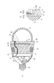
- FIG. 1 An exploded perspective view showing a configuration of a light source for illumination according to an embodiment of the present invention Sectional drawing which shows the structure of the light source for illumination which concerns on embodiment of this invention Top view for explaining the heat sink member and the contact portion of the mounting substrate
- Sectional drawing which shows the structure of the light source for illumination which concerns on the modification of this invention
- Sectional drawing which shows the structure of the light source for illumination which concerns on the modification of this invention
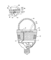
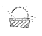
- FIG. 1 is an exploded perspective view showing a configuration of a light source for illumination according to an embodiment of the present invention.
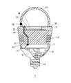
- FIG. 2 is a cross-sectional view showing the configuration of the illumination light source according to the embodiment of the present invention.
- the illumination light source 1 has a bowl-shaped case 15 in which an E-type cap 16 is formed to protrude, a heat sink member 11 fixed in a state of closing the opening of the case 15, and an upper surface of the heat sink member 11
- the mounting substrate 21 disposed on the surface facing the opening sealing surface 14, the light emitting unit 24 disposed on the top surface of the mounting substrate 21 (the surface facing the contact surface to the heat sink member 11), the heat sink member 11
- the heat sink member 31 disposed on the upper surface 14 of the above, and the globe 41 which is fixed to the heat sink member 31 and covers the light emitting direction of the light emitting portion 24 are provided. Further, as shown in FIG.
- a power supply circuit 18 for supplying commercial power supplied through the E-type cap 16 to the light emitting unit 24 is housed inside the case 15.
- the power supply circuit 18 is one in which various electronic components are mounted on the printed wiring board 17, and the printed wiring board 17 is fixed inside the case 15.
- the power supply circuit 18 and the light emitting unit 24 are electrically connected through the wiring 19.
- the wires 19 are passed through the through holes 13 provided in the heat sink member 11 and the through holes 33 provided in the heat sink member 31.
- the case 15 is made of resin, ceramic or the like and has electrical insulation.
- a bowl shape refers to the whole shape which has an opening at the end on the opposite side to the end where the E-type mouth ring 16 is provided, and the shape of the opening is not particularly limited to a circle.
- the heat sink member 11 is made of metal, for example, anodized aluminum, and the fins 12 are formed on the side of the substantially truncated cone shape and the upper surface 14 is flat. Further, a through hole 13 for introducing a wire is bored.
- the mounting substrate 21 is configured of a metal substrate 22 made of aluminum, copper or the like, and an insulating layer 23 made of resin, ceramics, etc. laminated on the upper surface of the metal substrate 22 (the surface facing the contact surface to the heat sink member 11). It is done.
- the light emitting unit 24 and the electrode pad 27 are mounted on the insulating layer 23.
- the peripheral portion 28 on the upper surface of the mounting substrate 21 is a region in which the light emitting unit 24 is not provided. In the peripheral portion 28, the insulating layer 23 is not present, and the upper surface of the metal substrate 22 is exposed.
- the light emitting portion 24 is configured of the LED 25 and the silicone resin molded body 26 (see an enlarged view of a portion A in FIG. 2).
- the LED 25 is a light emitting element that emits blue light.
- the silicone resin molded body 26 contains a yellow phosphor and functions as a wavelength conversion member that converts blue light into yellow light.
- the heat sink member 31 is, for example, a substantially disc-shaped flat plate made of metal such as anodized aluminum, and the lower surface thereof is formed in an opening 32 having a recess 34 and a part of the recess 34 penetrating to the upper surface It is done.
- the lower surface of the heat sink member 31 is in surface contact with the upper surface 14 of the heat sink member 11.
- the recessed portion 34 of the heat sink member 31 is formed so as to accommodate the mounting substrate 21 and to be in surface contact with the peripheral edge portion 28 of the upper surface of the mounting substrate 21.
- the opening 32 of the heat sink member 31 is formed to accommodate the light emitting unit 24.
- the globe 41 is made of a translucent resin, glass or the like, and is provided above the light emitting portion 24 and the mounting substrate 21 in order to protect the light emitting portion 24 and the mounting substrate 21 from direct contact with the user and scattering of water and the like. Is attached to the heat sink member 31 so as to cover the The globe 41 is attached to the upper surface of the heat sink member 31 with a thermally conductive bonding material, or screwed into a screw groove provided in the heat sink member 31. The peripheral edge portion 35 of the heat sink member 31 is not covered by the globe 41, and is in contact with the outside air (see FIG. 2).
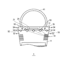
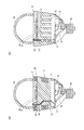
- FIG. 3 is a top view for explaining the contact portion of the heat sink member and the mounting substrate.
- the contact area between the mounting substrate 21 and the heat sink member 31 is larger than the area where the light emitting portion 24 which is a heat source is disposed.
- the mounting substrate 21 is a square in top view, and the heat sink member 31 is in surface contact with the three sides of the peripheral portion 28 of the mounting substrate 21. If a metal-based mounting substrate is employed as the mounting substrate on which the light emitting portion is disposed, better heat radiation characteristics can be obtained as compared to the case where a ceramic substrate is employed. However, the metal-based mounting substrate has a disadvantage that when a temperature difference occurs between the upper surface and the lower surface, internal stress is generated due to the difference in thermal expansion amount to cause warpage. If the mounting substrate is warped, the contact area between the lower surface of the mounting substrate and the heat sink member is narrowed, and the heat dissipation characteristics are degraded.
- the heat sink member 31 since the heat sink member 31 is in surface contact with the upper surface of the mounting substrate 21, the heat sink member 31 exerts an effect of suppressing the temperature difference between the upper surface and the lower surface of the mounting substrate 21. Even if stress is generated, the upper surface of the mounting substrate 21 can be pressed to exert the effect of restricting warpage. Furthermore, in the present embodiment, since the heat sink member 31 is in surface contact with the three sides of the peripheral edge portion 28 of the mounting substrate 21, the effect of restricting the warp of the mounting substrate 21 can be further enhanced.
- the thickness T2 of the portion of the heat sink member 31 in surface contact with the upper surface of the mounting substrate 21 is larger than the thickness T1 of the mounting substrate 21 (see the enlarged view of A in FIG. 2).
- the rigidity of the heat sink member 31 can be enhanced, and the effect of controlling the warpage of the mounting substrate 21 can be further enhanced.
- the heat sink member 31 is in direct contact with the metal substrate 22 without the interposition of the insulating layer 23 (see an enlarged view of a portion A in FIG. 2). Therefore, the thermal resistance at the interface between the mounting substrate 21 and the heat sink member 31 can be reduced, and good heat dissipation characteristics can be realized.
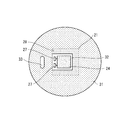
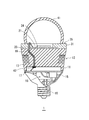
- FIG. 4 is a view showing a heat radiation path of the illumination light source according to the embodiment of the present invention.
- heat is conducted to the heat sink member 11 starting from the lower surface (symbol 51), natural air cooling from the heat sink member 11 (symbol 52) is conducted, and heat is conducted to the heat sink member 31 from the top surface (symbol 53), heat is conducted from the heat sink member 31 to the heat sink member 31 from the heat sink member 31 to the natural air cooling (code 54) path and the upper surface as the starting point (code 53); ), A path for natural air cooling from the heat sink member 11 (reference numeral 52) is formed. As described above, in the present embodiment, not only the lower surface of the mounting substrate 21 but also the heat dissipation path starting from the upper surface are formed.
- the heat radiation characteristics when the heat radiation path starting from the upper surface of the mounting substrate 21 is formed will be verified based on the experimental results.
- the inventors first conducted an experiment on the change of the heat radiation characteristic when the envelope volume of the heat sink member disposed on the lower surface of the mounting substrate is changed.
- FIG. 5 is a view schematically showing an experimental system of heat dissipation characteristics.
- the sample of the LED module is manufactured by arranging the light emitting unit 64 on the mounting substrate 62.
- a heat sink member 61 is disposed on the lower surface of the mounting substrate 62.
- An alumina substrate is adopted as the mounting substrate 62, and a 1.0 mm square LED chip is adopted as a light emitting element of the light emitting portion 64. Twelve LED chips are flip chip mounted on the alumina substrate.
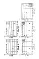
- FIG. 6 is a graph showing the measured temperature and junction temperature at each position, and (a) shows the sample top surface Pos. (B) shows the heat sink member top surface Pos. (C) shows the heat sink member end upper surface Pos. 3 shows the temperature of (3), (d) is the heat sink member lower surface Pos. (E) shows the junction temperature of the LED chip.
- the temperature at each position becomes lower as the envelope volume of the heat sink member disposed on the lower surface of the mounting substrate is larger.
- the effect of temperature reduction by increasing the envelope volume gradually decreases as the envelope volume increases.
- the sample top surface Pos. In No. 1 when the envelope volume of the heat sink member is changed from 54 cm 3 to 208 cm 3 , an excellent temperature drop effect can be obtained.
- the envelope volume of the heat sink member is changed from 1108.8 cm 3 to 2625 cm 3 , the effect of temperature drop is hardly obtained.
- Such tendency is shown in the sample horizontal Pos. 2.
- Tj At the junction temperature Tj, the sample top surface Pos. The same tendency as 1 is seen.
- the effect of temperature reduction can be obtained by increasing the envelope volume of the heat sink member disposed on the lower surface of the mounting substrate, but it is understood that there is also a limit. It is presumed that the heat radiation effect is regulated by the envelope volume when the envelope volume of the heat sink member is small, and that the radiation effect is regulated by the contact area between the heat sink member and the mounting substrate when the envelope volume is large to a certain extent. Be done. Based on the above experimental results, the inventors conducted an experiment on the change of the heat release characteristic when the contact area between the heat sink member and the mounting substrate is changed while the envelope volume remains the same.
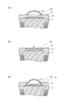
- FIG. 7 is a diagram schematically showing an experimental system of heat dissipation characteristics, (a) shows a sample size of the LED module, (b) shows a version 1 system, and (c) shows a version 2 system (D) shows a version 3 system.
- the heat sink member is disposed only on the lower surface of the mounting substrate, and the envelope volume of the heat sink member is 200 cm 3 .
- the heat sink member is disposed only on the lower surface of the mounting substrate, and the envelope volume of the heat sink member is 300 cm 3 .
- the heat sink members are disposed on the lower surface and the upper surface of the mounting substrate, and the envelope volume of the heat sink member is 300 cm 3 .
- FIG. 8 is a graph showing the measured temperature in each version.
- the above versions 1 and 2 correspond to the conventional example, and version 3 corresponds to the present embodiment. Therefore, the present embodiment can obtain better heat radiation characteristics than the conventional one, and can contribute to the downsizing of the illumination light source.
- the electrode pad 27 is provided on the upper surface of the mounting substrate 21, and the wiring 19 is connected to the electrode pad 27 on the upper surface of the mounting substrate 21.
- the present invention is not limited to this.
- the electrode pad 27 is provided on the lower surface of the mounting substrate 21, the wiring pattern 29 and the electrode pad 27 are electrically connected by through holes, and the wiring 19 is an electrode on the lower surface of the mounting substrate 21. It may be connected to the pad 27.
- the heat sink member 31 is not provided with a fin, but the present invention is not limited to this.
- the fins 36 may be provided on the side of the heat sink member 31.
- the fin is provided in the side part in the heat sink member 11 in embodiment, this invention is not limited to this.
- FIG. 12A the fins 36 may be provided on the side of the heat sink member 31.
- the fins 12 may be provided inside the heat sink member 11.
- the globe 41 has a shape similar to a light bulb, but the present invention is not limited thereto.
- the globe 41 may be made as small as possible, and the portion of the heat sink member 31 in contact with the outside air may be made large.
- the inner circumference of the opening of the heat sink member 31 is constant everywhere, the present invention is not limited to this.
- the opening may have an inner circumferential surface 37 which gradually widens as it approaches the top surface of the heat sink member. This can enhance the light extraction efficiency.
- a metal-based mounting substrate is used, but the present invention is not limited to this.
- the same effect can be obtained with a ceramic substrate such as an alumina substrate.
- the upper surface of the heat sink member 11 is a flat surface
- the lower surface of the heat sink member 31 has a recess for accommodating the mounting substrate 21.
- a recess for accommodating the mounting substrate 21 may be provided on the top surface of the heat sink member 11, and the heat sink member 31 may be provided with only an opening for receiving the light emitting portion 24 and extracting the light.
- recessed portions may be provided on both the upper surface of the heat sink member 11 and the lower surface of the heat sink member 31, and the mounting substrate 21 may be accommodated in both of the recessed portions.
- the light emitting unit 24 is completely accommodated in the opening of the heat sink member 31, but the present invention is not limited to this.
- the surface 39 of the top of the light emitting unit 24 may protrude in the direction perpendicular to the insulating substrate 21 more than the surface 38 of the heat sink member 31. By doing so, the light extraction efficiency can be enhanced.
- the rigidity of the heat sink member 31 is enhanced to secure the effect of restricting the warp of the mounting substrate 21.
- the gas in the inner space of the glove 41 is not mentioned, air or nitrogen gas may be sealed. Since nitrogen gas has better thermal conductivity than air, better heat dissipation characteristics can be obtained when nitrogen gas is enclosed. Moreover, it can prevent that a luminescent property degrades by moisture absorption of LED and a fluorescent substance.
- the sealing of the internal space of the glove 41 can be realized, for example, by the aspect shown in FIGS.
- the opening of the through hole 13 provided in the heat sink 11 is sealed with a sealing material 43
- the sealing valve 42 is provided in the globe 41.
- the sealing valve 42 is provided at the opening of the through hole 13.
- the sealing valve 42 is provided at the opening of the through hole 33.
- a mechanical vacuum valve or the like can be used as the sealing valve 42. Glass, resin, cement or the like can be used as the sealing material 43.
- the LED 25 is sealed by the silicone resin molded body 26.
- the present invention is not limited to this.
- the LED 25 may be exposed.
- the phosphor layer 44 on the inner surface of the glove 41, white light can be obtained as in the embodiment. Further, in order to prevent the LED and the phosphor from absorbing moisture, it is desirable to enclose nitrogen gas or dry air in the internal space of the glove 41 or to evacuate the internal gas and keep it in a vacuum state.
- the present invention can be widely used in lighting in general.
Abstract
Description
<構成>
図1は、本発明の実施形態に係る照明用光源の構成を示す分解斜視図である。図2は、本発明の実施形態に係る照明用光源の構成を示す断面図である。
<検証>
発明者らは、まず実装基板の下面に配設されたヒートシンク部材の包絡体積を変化させたときの放熱特性の変化に関する実験を行った。
(1)実施形態では、電極パッド27が実装基板21の上面に設けられており、配線19は実装基板21の上面の電極パッド27に接続されている。しかしながら本発明はこれに限られない。例えば、図9に示すように、実装基板21の下面に電極パッド27を設け、配線パターン29と電極パッド27とをスルーホールにて電気的に接続し、配線19を実装基板21の下面の電極パッド27に接続することとしてもよい。このようにすることで、図10に示すように実装基板21の上面における発光部が配設されていない領域を広げることができ、実装基板21の四辺にヒートシンク部材31を面接触させることができる。また図11に示すように、実装基板21の上面から下面にかけて貫通孔を穿設し、この貫通孔に配線19を通すこととしてもよい。
(2)実施形態では、ヒートシンク部材31にはフィンが設けられていないが、本発明はこれに限られない。例えば、図12(a)に示すように、ヒートシンク部材31の側部にフィン36を設けることとしてもよい。また実施の形態では、ヒートシンク部材11には側部にフィンが設けられているが、本発明はこれに限られない。例えば、図12(b)に示すように、ヒートシンク部材11の内部にフィン12を設けることとしてもよい。
(3)実施形態では、グローブ41を電球形に類似した形状としているが、本発明はこれに限られない。例えば、図13に示すように、グローブ41をできるだけ小さくして、ヒートシンク部材31が外気に触れる部分を大きくしてもよい。
(4)実施形態では、ヒートシンク部材31の開口の内周はどこでも一定であるが、本発明はこれに限られない。例えば、図14に示すように、開口がヒートシンク部材上面に近づくにつれて次第に広がる内周面37を有することとしてもよい。これにより光の取出し効率を高めることができる。
(5)実施形態では、金属ベースの実装基板を用いているが、本発明はこれに限られない。例えば、アルミナ基板等のセラミックス基板でも同様の効果を得ることができる。
(6)実施形態では、ヒートシンク部材11の上面が平坦面であり、ヒートシンク部材31の下面が実装基板21を収容するための凹入部をもつが、本発明はこれに限られない。例えば、ヒートシンク部材11の上面に実装基板21を収容するための凹入部を設け、ヒートシンク部材31には発光部24を収容して光を取出すための開口のみを設けることとしてもよい。またヒートシンク部材11の上面およびヒートシンク部材31の下面の両方に凹入部を設け、両方の凹入部で実装基板21を収容することとしてもよい。
(7)実施形態では、発光部24はヒートシンク部材31の開口に完全に収容されているが、本発明はこれに限られない。例えば、図15に示すように、発光部24の頂部の面39がヒートシンク部材31の表面38よりも絶縁基板21に垂直な方向に突出していてもよい。そうすることで光取出し効率を高めることができる。なお、この場合においても、ヒートシンク部材31の厚みT2を実装基板21の厚みT1よりも大きくしておくことにより、ヒートシンク部材31の剛性を高めて実装基板21の反りを規制する効果を確保することができる。
(8)実施形態では、グローブ41の内部空間のガスについて言及していないが、空気でもよいし窒素ガスを封入することとしてもよい。窒素ガスは空気に比べて熱伝導性が良いので、窒素ガスを封入した場合にはさらに良好な放熱特性を得ることができる。また、LEDおよび蛍光体が吸湿することにより発光特性が劣化してしまうことを防止することができる。
(9)実施形態では、LED25はシリコーン樹脂成形体26により封止されているが、本発明は、これに限らない。例えば、図18に示すように、LED25が露出していてもよい。この場合、グローブ41の内面に蛍光体層44を設けることにより、実施形態同様に白色光を得ることができる。また、LEDおよび蛍光体が吸湿することを防止するため、グローブ41の内部空間に窒素ガスや乾燥空気を封入するか、内部のガスを排気して真空状態にしておくのが望ましい。
11 ヒートシンク部材
12 フィン
13 貫通孔
14 上面
15 ケース
16 E型口金
17 プリント配線板
18 電源回路
19 配線
21 実装基板
22 金属基板
23 絶縁層
24 発光部
25 LED
26 シリコーン樹脂成形体
27 電極パッド
28 周縁部
29 配線パターン
31 ヒートシンク部材
32 開口
33 貫通孔
34 凹入部
35 周縁部
36 フィン
37 次第に広がる内周面
38 ヒートシンク部材の表面
39 発光部の頂部の面
41 グローブ
42 封止弁
43 封止部材
44 蛍光体層
61 ヒートシンク部材
62 実装基板
64 発光部
Claims (10)
- 口金を通じて電力供給を受ける電球形照明用光源であって、
口金が突設形成されていると共に内部に電源回路を収容している椀状ケースと、
前記椀状ケースの開口を封塞する状態で固定された第1のヒートシンク部材と、
前記第1のヒートシンク部材の開口封塞面に対向する表面に面接触させて配置された実装基板と、
前記実装基板の前記第1のヒートシンク部材への接触面に対向する表面に実装され、前記電源回路から電力供給を受けて発光する発光素子および当該発光素子から出射された光の波長を変換する波長変換部材を含む発光部と、
少なくとも前記発光部の光射出方向を覆うグローブと、
実装基板の前記表面における前記発光部が配設されていない領域に面接触する第1部分と前記第1のヒートシンク部材に面接触する第2部分とを有する第2のヒートシンク部材と
を備えることを特徴とする電球形照明用光源。 - 前記第2のヒートシンク部材の少なくとも一部は、前記グローブに覆われずに外部に露出していること
を特徴とする請求項1に記載の電球形照明用光源。 - 前記第2のヒートシンク部材は、平板であり、その一方の主面が前記第2の部分であり、前記主面の一部が凹入されて前記第1の部分が形成されていると共に、凹入部の一部が他方の主面まで貫通する開口に形成され、当該開口に前記発光部が収容されていること
を特徴とする請求項1に記載の電球形照明用光源。 - 前記開口の内周は、前記他方の主面に近づくにつれて次第に広がること
を特徴とする請求項3に記載の電球形照明用光源。 - 前記第2のヒートシンク部材と前記実装基板との接触面積は、前記発光部と前記実装基板との接触面積よりも広いこと
を特徴とする請求項1に記載の電球形照明用光源。 - 前記第2のヒートシンク部材における前記第1部分は、実装基板の前記表面における周縁部全周にわたり面接触しており、または、実装基板の前記表面に配された電極パッド付近を除いて全周にわたり面接触していること
を特徴とする請求項1に記載の電球形照明用光源。 - 前記第2のヒートシンク部材における前記第1部分の厚みは、前記実装基板の厚みよりも大きいこと
を特徴とする請求項1に記載の電球形照明用光源。 - 前記実装基板は、前記第1のヒートシンク部材の開口封塞面に対向する表面に面接触させて配置された金属基板と、当該金属基板の前記第1のヒートシンク部材への接触面に対向する表面の一部領域に積層された絶縁層とから構成され、
前記発光部は、前記絶縁層に配設されており、
前記第2のヒートシンク部材における前記第1部分は、前記金属基板の前記表面における前記絶縁層が積層されていない領域に面接触していること
を特徴とする請求項1に記載の電球形照明用光源。 - 前記グローブは、前記第2のヒートシンク部材に設けられたねじ溝にねじ嵌めされ、または、熱伝導性接合材で接合されて、前記第2のヒートシンク部材に連結されていること
を特徴とする請求項1に記載の電球形照明用光源。 - 前記発光部の頂部は、前記第2のヒートシンク部材の表面よりも実装基板に垂直な方向に突出していること
を特徴とする請求項1に記載の電球形照明用光源。
Priority Applications (4)
| Application Number | Priority Date | Filing Date | Title |
|---|---|---|---|
| EP09794150.4A EP2309168B1 (en) | 2008-07-07 | 2009-06-30 | Bulb-type lighting source |
| US12/996,523 US8337049B2 (en) | 2008-07-07 | 2009-06-30 | Bulb-type lighting source |
| CN200980126425.4A CN102089567B (zh) | 2008-07-07 | 2009-06-30 | 灯泡形照明用光源 |
| JP2010519630A JP5129329B2 (ja) | 2008-07-07 | 2009-06-30 | 電球形照明用光源 |
Applications Claiming Priority (2)
| Application Number | Priority Date | Filing Date | Title |
|---|---|---|---|
| JP2008-176916 | 2008-07-07 | ||
| JP2008176916 | 2008-07-07 |
Publications (1)
| Publication Number | Publication Date |
|---|---|
| WO2010004702A1 true WO2010004702A1 (ja) | 2010-01-14 |
Family
ID=41506830
Family Applications (1)
| Application Number | Title | Priority Date | Filing Date |
|---|---|---|---|
| PCT/JP2009/003015 WO2010004702A1 (ja) | 2008-07-07 | 2009-06-30 | 電球形照明用光源 |
Country Status (6)
| Country | Link |
|---|---|
| US (1) | US8337049B2 (ja) |
| EP (1) | EP2309168B1 (ja) |
| JP (2) | JP5129329B2 (ja) |
| KR (1) | KR101217201B1 (ja) |
| CN (1) | CN102089567B (ja) |
| WO (1) | WO2010004702A1 (ja) |
Cited By (15)
| Publication number | Priority date | Publication date | Assignee | Title |
|---|---|---|---|---|
| DE102010001047A1 (de) * | 2010-01-20 | 2011-07-21 | Osram Gesellschaft mit beschränkter Haftung, 81543 | Leuchtvorrichtung |
| WO2011132399A1 (ja) * | 2010-04-19 | 2011-10-27 | パナソニック株式会社 | ガラス組成物、光源装置および照明装置 |
| JP2011243502A (ja) * | 2010-05-20 | 2011-12-01 | Ichikoh Ind Ltd | 車両用灯具 |
| JP2012059636A (ja) * | 2010-09-10 | 2012-03-22 | Sharp Corp | 照明装置 |
| JP2012099335A (ja) * | 2010-11-02 | 2012-05-24 | Rohm Co Ltd | Led電球 |
| WO2012095931A1 (ja) * | 2011-01-14 | 2012-07-19 | パナソニック株式会社 | ランプ及び照明装置 |
| JP2012227143A (ja) * | 2011-04-15 | 2012-11-15 | Lextar Electronics Corp | 発光ダイオードカップ灯 |
| CN102792087A (zh) * | 2010-03-22 | 2012-11-21 | 欧司朗股份有限公司 | 具有反射机构和反射元件的灯 |
| US20130077318A1 (en) * | 2010-05-31 | 2013-03-28 | Sharp Kabushiki Kaisha | Lighting apparatus |
| JPWO2011132402A1 (ja) * | 2010-04-19 | 2013-07-18 | パナソニック株式会社 | ガラス組成物、光源装置および照明装置 |
| JP5379335B1 (ja) * | 2012-07-05 | 2013-12-25 | パナソニック株式会社 | ランプ及び照明装置 |
| JP2014099423A (ja) * | 2014-03-07 | 2014-05-29 | Sharp Corp | 電球型の照明装置 |
| JP2014132584A (ja) * | 2014-02-24 | 2014-07-17 | Sharp Corp | 照明装置 |
| US20140247598A1 (en) * | 2012-02-02 | 2014-09-04 | Posco Led Company Ltd. | Heat sink and led illuminating apparatus comprising the same |
| WO2015045814A1 (ja) * | 2013-09-24 | 2015-04-02 | 堺ディスプレイプロダクト株式会社 | 光源モジュール及び表示装置 |
Families Citing this family (23)
| Publication number | Priority date | Publication date | Assignee | Title |
|---|---|---|---|---|
| CN102175000B (zh) * | 2008-07-30 | 2013-11-06 | 东芝照明技术株式会社 | 灯装置及照明器具 |
| JP5573439B2 (ja) * | 2010-07-09 | 2014-08-20 | Tdk株式会社 | ワイヤレス給電装置、光源カートリッジおよびワイヤレス照明システム |
| US10400959B2 (en) * | 2010-11-09 | 2019-09-03 | Lumination Llc | LED lamp |
| KR101739379B1 (ko) | 2011-01-11 | 2017-05-24 | 삼성전자주식회사 | 디지털 촬영 장치 및 이의 제어 방법 |
| DE102011013052A1 (de) * | 2011-03-04 | 2012-09-06 | Osram Opto Semiconductors Gmbh | Verfahren zur Herstellung zumindest eines optoelektronischen Halbleiterbauelements |
| US8604684B2 (en) * | 2011-05-16 | 2013-12-10 | Cree, Inc. | UV stable optical element and LED lamp using same |
| WO2012160731A1 (ja) * | 2011-05-20 | 2012-11-29 | パナソニック株式会社 | ランプ |
| DE102011081672A1 (de) * | 2011-08-26 | 2013-02-28 | Osram Ag | Lichtquellenvorrichtung |
| FI20125933A (fi) * | 2012-09-08 | 2014-03-09 | Lumichip Ltd | LED-chip-on-board-komponentti ja -valaistusmoduuli |
| JP2014130777A (ja) * | 2012-12-28 | 2014-07-10 | Toshiba Lighting & Technology Corp | 照明装置 |
| JP2014146510A (ja) * | 2013-01-29 | 2014-08-14 | Panasonic Corp | 照明用光源および照明装置 |
| KR101347392B1 (ko) * | 2013-03-05 | 2014-01-06 | 주식회사 포스코엘이디 | 히트싱크 및 이를 포함하는 엘이디 조명장치 |
| KR101412959B1 (ko) * | 2013-07-05 | 2014-06-27 | 주식회사 포스코엘이디 | 엘이디 조명장치 |
| WO2015045206A1 (ja) * | 2013-09-25 | 2015-04-02 | パナソニックIpマネジメント株式会社 | 照明ユニット |
| JP2016153873A (ja) * | 2015-02-17 | 2016-08-25 | セイコーエプソン株式会社 | 波長変換装置、照明装置およびプロジェクター |
| US11686459B2 (en) | 2015-12-15 | 2023-06-27 | Wangs Alliance Corporation | LED lighting methods and apparatus |
| US10208935B2 (en) | 2015-12-15 | 2019-02-19 | Wangs Alliance Corporation | LED lighting apparatus with adjustable beam angle lens |
| DE102016203668A1 (de) * | 2016-03-07 | 2017-09-07 | Ledvance Gmbh | Retrofitlampe |
| US11056629B2 (en) * | 2017-03-21 | 2021-07-06 | Lumileds Llc | Mounting an LED element on a flat carrier |
| KR102137143B1 (ko) * | 2019-03-11 | 2020-07-24 | 엘지이노텍 주식회사 | 조명 장치 |
| US11598517B2 (en) | 2019-12-31 | 2023-03-07 | Lumien Enterprise, Inc. | Electronic module group |
| CN110985903B (zh) | 2019-12-31 | 2020-08-14 | 江苏舒适照明有限公司 | 一种灯模组 |
| CN111503556B (zh) | 2020-04-23 | 2020-11-27 | 江苏舒适照明有限公司 | 一种射灯结构 |
Citations (10)
| Publication number | Priority date | Publication date | Assignee | Title |
|---|---|---|---|---|
| JPH0686359U (ja) * | 1993-05-31 | 1994-12-13 | オプトニクス株式会社 | Ledランプ |
| JP2002093206A (ja) * | 2000-09-18 | 2002-03-29 | Stanley Electric Co Ltd | Led信号灯具 |
| JP2002299700A (ja) * | 2001-04-02 | 2002-10-11 | Nichia Chem Ind Ltd | Led照明装置 |
| JP2003124528A (ja) | 2001-08-09 | 2003-04-25 | Matsushita Electric Ind Co Ltd | Led照明装置およびカード型led照明光源 |
| JP2004265619A (ja) | 2003-02-07 | 2004-09-24 | Matsushita Electric Ind Co Ltd | カード型led光源用回動ソケット |
| JP2005038798A (ja) | 2003-07-18 | 2005-02-10 | Matsushita Electric Ind Co Ltd | 照明装置及びランプモジュール |
| JP2005166578A (ja) * | 2003-12-05 | 2005-06-23 | Hamai Denkyu Kogyo Kk | 電球形ledランプ |
| JP2005294292A (ja) | 2004-03-31 | 2005-10-20 | Citizen Electronics Co Ltd | 発光装置及び発光装置の製造方法 |
| JP2006313717A (ja) * | 2005-04-08 | 2006-11-16 | Toshiba Lighting & Technology Corp | 電球型ランプ |
| JP3142963U (ja) * | 2008-04-21 | 2008-07-03 | 秦文隆 | 高効率ledランプ |
Family Cites Families (15)
| Publication number | Priority date | Publication date | Assignee | Title |
|---|---|---|---|---|
| JPH03142963A (ja) | 1989-10-30 | 1991-06-18 | Matsushita Electron Corp | 半導体装置 |
| JP3142963B2 (ja) | 1992-08-21 | 2001-03-07 | 三井化学株式会社 | 架橋ポリオレフィンの製造方法 |
| JP2806165B2 (ja) | 1992-08-31 | 1998-09-30 | 日本電気株式会社 | デジタル無線電話システムの追跡交換チャネル切替方法 |
| CN1464953A (zh) * | 2001-08-09 | 2003-12-31 | 松下电器产业株式会社 | Led照明装置和卡型led照明光源 |
| US6465961B1 (en) * | 2001-08-24 | 2002-10-15 | Cao Group, Inc. | Semiconductor light source using a heat sink with a plurality of panels |
| US20040256630A1 (en) * | 2001-08-24 | 2004-12-23 | Densen Cao | Illuminating light |
| JP2003124258A (ja) | 2001-10-09 | 2003-04-25 | Rohm Co Ltd | 半導体チップの実装方法、および半導体チップの実装構造 |
| DE602004028099D1 (de) * | 2003-02-07 | 2010-08-26 | Panasonic Corp | Beleuchtungseinrichtung, einen sockel verwendend, um ein flaches led-modul auf einen kühlkörper zu montieren |
| JP2007528588A (ja) * | 2003-09-16 | 2007-10-11 | 松下電器産業株式会社 | Led照明光源およびled照明装置 |
| US20060098440A1 (en) * | 2004-11-05 | 2006-05-11 | David Allen | Solid state lighting device with improved thermal management, improved power management, adjustable intensity, and interchangable lenses |
| JP2006156187A (ja) * | 2004-11-30 | 2006-06-15 | Mitsubishi Electric Corp | Led光源装置及びled電球 |
| CN2786421Y (zh) * | 2005-02-23 | 2006-06-07 | 李洲科技股份有限公司 | 发光二极体照明设备 |
| US7758223B2 (en) * | 2005-04-08 | 2010-07-20 | Toshiba Lighting & Technology Corporation | Lamp having outer shell to radiate heat of light source |
| JP5785361B2 (ja) * | 2006-11-30 | 2015-09-30 | クリー インコーポレイテッドCree Inc. | 安定器内蔵型固体照明装置 |
| CN200986121Y (zh) * | 2006-12-04 | 2007-12-05 | 品能科技股份有限公司 | 发光二极管灯泡结构 |
-
2009
- 2009-06-30 US US12/996,523 patent/US8337049B2/en active Active
- 2009-06-30 JP JP2010519630A patent/JP5129329B2/ja active Active
- 2009-06-30 KR KR1020107027355A patent/KR101217201B1/ko not_active IP Right Cessation
- 2009-06-30 CN CN200980126425.4A patent/CN102089567B/zh active Active
- 2009-06-30 WO PCT/JP2009/003015 patent/WO2010004702A1/ja active Application Filing
- 2009-06-30 EP EP09794150.4A patent/EP2309168B1/en not_active Not-in-force
-
2012
- 2012-07-17 JP JP2012158607A patent/JP5082019B1/ja active Active
Patent Citations (10)
| Publication number | Priority date | Publication date | Assignee | Title |
|---|---|---|---|---|
| JPH0686359U (ja) * | 1993-05-31 | 1994-12-13 | オプトニクス株式会社 | Ledランプ |
| JP2002093206A (ja) * | 2000-09-18 | 2002-03-29 | Stanley Electric Co Ltd | Led信号灯具 |
| JP2002299700A (ja) * | 2001-04-02 | 2002-10-11 | Nichia Chem Ind Ltd | Led照明装置 |
| JP2003124528A (ja) | 2001-08-09 | 2003-04-25 | Matsushita Electric Ind Co Ltd | Led照明装置およびカード型led照明光源 |
| JP2004265619A (ja) | 2003-02-07 | 2004-09-24 | Matsushita Electric Ind Co Ltd | カード型led光源用回動ソケット |
| JP2005038798A (ja) | 2003-07-18 | 2005-02-10 | Matsushita Electric Ind Co Ltd | 照明装置及びランプモジュール |
| JP2005166578A (ja) * | 2003-12-05 | 2005-06-23 | Hamai Denkyu Kogyo Kk | 電球形ledランプ |
| JP2005294292A (ja) | 2004-03-31 | 2005-10-20 | Citizen Electronics Co Ltd | 発光装置及び発光装置の製造方法 |
| JP2006313717A (ja) * | 2005-04-08 | 2006-11-16 | Toshiba Lighting & Technology Corp | 電球型ランプ |
| JP3142963U (ja) * | 2008-04-21 | 2008-07-03 | 秦文隆 | 高効率ledランプ |
Non-Patent Citations (1)
| Title |
|---|
| See also references of EP2309168A4 * |
Cited By (27)
| Publication number | Priority date | Publication date | Assignee | Title |
|---|---|---|---|---|
| CN102713409A (zh) * | 2010-01-20 | 2012-10-03 | 欧司朗股份有限公司 | 照明装置 |
| DE102010001047A1 (de) * | 2010-01-20 | 2011-07-21 | Osram Gesellschaft mit beschränkter Haftung, 81543 | Leuchtvorrichtung |
| CN102792087A (zh) * | 2010-03-22 | 2012-11-21 | 欧司朗股份有限公司 | 具有反射机构和反射元件的灯 |
| CN102803170A (zh) * | 2010-04-19 | 2012-11-28 | 松下电器产业株式会社 | 玻璃组合物、光源装置以及照明装置 |
| JP5842178B2 (ja) * | 2010-04-19 | 2016-01-13 | パナソニックIpマネジメント株式会社 | 光源装置および照明装置 |
| JP5828065B2 (ja) * | 2010-04-19 | 2015-12-02 | パナソニックIpマネジメント株式会社 | 光源装置および照明装置 |
| EP2562145A1 (en) * | 2010-04-19 | 2013-02-27 | Panasonic Corporation | Glass composition, light source device and illumination device |
| WO2011132399A1 (ja) * | 2010-04-19 | 2011-10-27 | パナソニック株式会社 | ガラス組成物、光源装置および照明装置 |
| JPWO2011132402A1 (ja) * | 2010-04-19 | 2013-07-18 | パナソニック株式会社 | ガラス組成物、光源装置および照明装置 |
| EP2562145A4 (en) * | 2010-04-19 | 2013-09-18 | Panasonic Corp | GLASS COMPOSITION, LIGHT SOURCE DEVICE AND LIGHTING DEVICE |
| JP2011243502A (ja) * | 2010-05-20 | 2011-12-01 | Ichikoh Ind Ltd | 車両用灯具 |
| US9562651B2 (en) * | 2010-05-31 | 2017-02-07 | Sharp Kabushiki Kaisha | Lighting apparatus |
| US20130077318A1 (en) * | 2010-05-31 | 2013-03-28 | Sharp Kabushiki Kaisha | Lighting apparatus |
| JP2012059636A (ja) * | 2010-09-10 | 2012-03-22 | Sharp Corp | 照明装置 |
| JP2012099335A (ja) * | 2010-11-02 | 2012-05-24 | Rohm Co Ltd | Led電球 |
| CN103080631A (zh) * | 2011-01-14 | 2013-05-01 | 松下电器产业株式会社 | 灯及照明装置 |
| WO2012095931A1 (ja) * | 2011-01-14 | 2012-07-19 | パナソニック株式会社 | ランプ及び照明装置 |
| US8690388B2 (en) | 2011-04-15 | 2014-04-08 | Lextar Electronics Corporation | Light emitting diode cup light |
| JP2012227143A (ja) * | 2011-04-15 | 2012-11-15 | Lextar Electronics Corp | 発光ダイオードカップ灯 |
| US20140247598A1 (en) * | 2012-02-02 | 2014-09-04 | Posco Led Company Ltd. | Heat sink and led illuminating apparatus comprising the same |
| JP2014029866A (ja) * | 2012-07-05 | 2014-02-13 | Panasonic Corp | ランプ及び照明装置 |
| JP5379335B1 (ja) * | 2012-07-05 | 2013-12-25 | パナソニック株式会社 | ランプ及び照明装置 |
| WO2015045814A1 (ja) * | 2013-09-24 | 2015-04-02 | 堺ディスプレイプロダクト株式会社 | 光源モジュール及び表示装置 |
| JPWO2015045814A1 (ja) * | 2013-09-24 | 2017-03-09 | 堺ディスプレイプロダクト株式会社 | 光源モジュール及び表示装置 |
| US9739932B2 (en) | 2013-09-24 | 2017-08-22 | Sakai Display Products Corporation | Light source module and display apparatus |
| JP2014132584A (ja) * | 2014-02-24 | 2014-07-17 | Sharp Corp | 照明装置 |
| JP2014099423A (ja) * | 2014-03-07 | 2014-05-29 | Sharp Corp | 電球型の照明装置 |
Also Published As
| Publication number | Publication date |
|---|---|
| EP2309168B1 (en) | 2015-09-23 |
| JP5129329B2 (ja) | 2013-01-30 |
| US20110090699A1 (en) | 2011-04-21 |
| JP2012238601A (ja) | 2012-12-06 |
| KR20110002883A (ko) | 2011-01-10 |
| JP5082019B1 (ja) | 2012-11-28 |
| EP2309168A1 (en) | 2011-04-13 |
| CN102089567B (zh) | 2014-02-26 |
| EP2309168A4 (en) | 2013-12-04 |
| KR101217201B1 (ko) | 2012-12-31 |
| US8337049B2 (en) | 2012-12-25 |
| JPWO2010004702A1 (ja) | 2011-12-22 |
| CN102089567A (zh) | 2011-06-08 |
Similar Documents
| Publication | Publication Date | Title |
|---|---|---|
| WO2010004702A1 (ja) | 電球形照明用光源 | |
| KR101032415B1 (ko) | 방사형 방열장치 및 이를 이용한 전구형 led 조명장치 | |
| JP4840185B2 (ja) | 照明装置 | |
| JP5508113B2 (ja) | ランプ及び照明装置 | |
| JP5029822B2 (ja) | 光源および照明装置 | |
| JP5327472B2 (ja) | 電球形ランプおよび照明器具 | |
| JP2010016223A (ja) | ランプ | |
| TW201102577A (en) | Bulb-shaped lamp and illumination device | |
| JP2010045030A (ja) | 発光ダイオード照明装置 | |
| TWM382586U (en) | Hermetic light emitting device | |
| TW201243235A (en) | Lighting device | |
| JP2007324547A (ja) | 発光ダイオード光源装置、照明装置、表示装置及び交通信号機 | |
| KR101038213B1 (ko) | 고휘도 엘이디용 쾌속 방열장치 | |
| JP2015076281A (ja) | 照明装置 | |
| WO2012008175A1 (ja) | 照明装置 | |
| JP2008153466A (ja) | 発光装置 | |
| TWI500881B (zh) | 燈具 | |
| KR20130025718A (ko) | 엘이디 램프 | |
| JP2012146552A (ja) | 照明装置 | |
| TWM482691U (zh) | 燈具 | |
| JP2016134571A (ja) | 発光装置および照明装置 | |
| TWM496094U (zh) | 燈具 | |
| JP5582365B2 (ja) | 照明装置 | |
| KR101611391B1 (ko) | 절연 방열판이 구비된 led등 | |
| WO2016021354A1 (ja) | 発光装置、照明装置、および発光装置の製造方法 |
Legal Events
| Date | Code | Title | Description |
|---|---|---|---|
| WWE | Wipo information: entry into national phase |
Ref document number: 200980126425.4 Country of ref document: CN |
|
| 121 | Ep: the epo has been informed by wipo that ep was designated in this application |
Ref document number: 09794150 Country of ref document: EP Kind code of ref document: A1 |
|
| WWE | Wipo information: entry into national phase |
Ref document number: 2010519630 Country of ref document: JP |
|
| ENP | Entry into the national phase |
Ref document number: 20107027355 Country of ref document: KR Kind code of ref document: A |
|
| WWE | Wipo information: entry into national phase |
Ref document number: 12996523 Country of ref document: US |
|
| WWE | Wipo information: entry into national phase |
Ref document number: 2009794150 Country of ref document: EP |
|
| NENP | Non-entry into the national phase |
Ref country code: DE |