WO2006070602A1 - 導電性エンドレスベルト、その製造方法およびそれを用いた画像形成装置 - Google Patents
導電性エンドレスベルト、その製造方法およびそれを用いた画像形成装置 Download PDFInfo
- Publication number
- WO2006070602A1 WO2006070602A1 PCT/JP2005/022977 JP2005022977W WO2006070602A1 WO 2006070602 A1 WO2006070602 A1 WO 2006070602A1 JP 2005022977 W JP2005022977 W JP 2005022977W WO 2006070602 A1 WO2006070602 A1 WO 2006070602A1
- Authority
- WO
- WIPO (PCT)
- Prior art keywords
- endless belt
- conductive endless
- curable resin
- resin
- conductive
- Prior art date
- Legal status (The legal status is an assumption and is not a legal conclusion. Google has not performed a legal analysis and makes no representation as to the accuracy of the status listed.)
- Ceased
Links
Classifications
-
- B—PERFORMING OPERATIONS; TRANSPORTING
- B29—WORKING OF PLASTICS; WORKING OF SUBSTANCES IN A PLASTIC STATE IN GENERAL
- B29D—PRODUCING PARTICULAR ARTICLES FROM PLASTICS OR FROM SUBSTANCES IN A PLASTIC STATE
- B29D29/00—Producing belts or bands
-
- G—PHYSICS
- G03—PHOTOGRAPHY; CINEMATOGRAPHY; ANALOGOUS TECHNIQUES USING WAVES OTHER THAN OPTICAL WAVES; ELECTROGRAPHY; HOLOGRAPHY
- G03G—ELECTROGRAPHY; ELECTROPHOTOGRAPHY; MAGNETOGRAPHY
- G03G15/00—Apparatus for electrographic processes using a charge pattern
- G03G15/01—Apparatus for electrographic processes using a charge pattern for producing multicoloured copies
-
- G—PHYSICS
- G03—PHOTOGRAPHY; CINEMATOGRAPHY; ANALOGOUS TECHNIQUES USING WAVES OTHER THAN OPTICAL WAVES; ELECTROGRAPHY; HOLOGRAPHY
- G03G—ELECTROGRAPHY; ELECTROPHOTOGRAPHY; MAGNETOGRAPHY
- G03G15/00—Apparatus for electrographic processes using a charge pattern
- G03G15/14—Apparatus for electrographic processes using a charge pattern for transferring a pattern to a second base
- G03G15/16—Apparatus for electrographic processes using a charge pattern for transferring a pattern to a second base of a toner pattern, e.g. a powder pattern, e.g. magnetic transfer
- G03G15/1665—Apparatus for electrographic processes using a charge pattern for transferring a pattern to a second base of a toner pattern, e.g. a powder pattern, e.g. magnetic transfer by introducing the second base in the nip formed by the recording member and at least one transfer member, e.g. in combination with bias or heat
- G03G15/167—Apparatus for electrographic processes using a charge pattern for transferring a pattern to a second base of a toner pattern, e.g. a powder pattern, e.g. magnetic transfer by introducing the second base in the nip formed by the recording member and at least one transfer member, e.g. in combination with bias or heat at least one of the recording member or the transfer member being rotatable during the transfer
- G03G15/1685—Structure, details of the transfer member, e.g. chemical composition
-
- G—PHYSICS
- G03—PHOTOGRAPHY; CINEMATOGRAPHY; ANALOGOUS TECHNIQUES USING WAVES OTHER THAN OPTICAL WAVES; ELECTROGRAPHY; HOLOGRAPHY
- G03G—ELECTROGRAPHY; ELECTROPHOTOGRAPHY; MAGNETOGRAPHY
- G03G2215/00—Apparatus for electrophotographic processes
- G03G2215/01—Apparatus for electrophotographic processes for producing multicoloured copies
- G03G2215/0103—Plural electrographic recording members
- G03G2215/0119—Linear arrangement adjacent plural transfer points
-
- G—PHYSICS
- G03—PHOTOGRAPHY; CINEMATOGRAPHY; ANALOGOUS TECHNIQUES USING WAVES OTHER THAN OPTICAL WAVES; ELECTROGRAPHY; HOLOGRAPHY
- G03G—ELECTROGRAPHY; ELECTROPHOTOGRAPHY; MAGNETOGRAPHY
- G03G2215/00—Apparatus for electrophotographic processes
- G03G2215/01—Apparatus for electrophotographic processes for producing multicoloured copies
- G03G2215/0167—Apparatus for electrophotographic processes for producing multicoloured copies single electrographic recording member
- G03G2215/0174—Apparatus for electrophotographic processes for producing multicoloured copies single electrographic recording member plural rotations of recording member to produce multicoloured copy
- G03G2215/0177—Rotating set of developing units
Definitions
- the present invention relates to an electrostatic recording process in an electrophotographic apparatus such as a copying machine or a printer, an electrostatic recording apparatus or the like, and a latent image holding body that holds an electrostatic latent image on the surface.
- Conductive endless belt (hereinafter also simply referred to as “belt”) used for transferring a toner image formed by supplying a developer to the surface of an image forming body onto a recording medium such as paper, and its manufacture
- the present invention relates to a method and an image forming apparatus using the method.
- four toner images are formed: a magenta toner image, a yellow toner image, a cyan toner image, and a black toner image.
- There is a tandem system that reproduces a color image by arranging the toner images in a row and sequentially transferring the toner images onto a recording medium such as paper and overlaying them on the recording medium.
- FIG. 2 shows a configuration example of a printing unit of a tandem image forming apparatus.
- the printing unit consisting of photosensitive drum 1, charging roll 2, developing roll 3, developing blade 4, toner supply roll 5 and cleaning blade 6 is compatible with yellow Y, magenta ⁇ , cyan C, and black B toner.
- the four toners are arranged side by side, and the toner is sequentially transferred onto a sheet that is circulated by a driving roller (driving member) 9 and conveyed by the transfer conveying belt 10 to form a color image.
- Charging and discharging of the transfer conveyor belt are performed by the charging roll 7 and the discharging roll 8, respectively.
- a suction roller (not shown) is used for charging the paper for sucking the paper onto the belt.
- the suction roller places the paper on the transfer / conveyance belt as well as the conveyance path and electrostatically attracts the transfer / conveyance belt. Further, the paper separation after the transfer can be performed only by the curvature separation by lowering the transfer voltage to weaken the adsorbing force between the paper and the transfer conveyance belt.
- the material of the transfer conveyance belt 10 includes a resistor and a dielectric, each having advantages and disadvantages.
- Resistor belts hold charge for a short time, so when used for tandem transfer, there is little charge injection during transfer, and the voltage rise is relatively small even during continuous transfer of four colors. Also, when it is repeatedly used for the next paper transfer, the electric charge is released, and no electrical reset is required.
- the resistance value changes due to environmental changes, it has the disadvantages of affecting transfer efficiency and being susceptible to paper thickness and width.
- a recording medium such as paper is wound around a transfer drum and rotated four times, and magenta, yellow, cyan, and black on the photosensitive member are sequentially transferred to the recording medium every turn so that a color image is obtained.
- a transfer drum system that reproduces. According to this method, a relatively high image quality can be obtained.
- the recording medium is a cardboard such as a postcard, it is difficult to wrap it around the transfer drum, and the type of recording medium is limited. There is a problem.
- an intermediate transfer member composed of a drum and a belt for temporarily transferring and holding a toner image on a photosensitive member
- a magenta toner image and a yellow toner image are provided around the intermediate transfer member.
- a color image is formed on the intermediate transfer member by arranging four photoconductors that form a cyan toner image and a black toner image and sequentially transferring the four color toner images onto the intermediate transfer member.
- the color image is transferred onto a recording medium such as paper. Therefore, it is possible to obtain high image quality with the power of adjusting the gradation by superimposing the four color toner images, and it is not necessary to arrange the photoconductors in a single row as in the tandem method. There is no need to limit the size of the recording medium because the apparatus is not particularly large and does not need to be rubbed or wound around the drum.
- FIG. 3 illustrates an image forming apparatus using an endless belt-shaped intermediate transfer member as an intermediate transfer member as an apparatus for forming a color image by an intermediate transfer method.
- reference numeral 11 denotes a drum-shaped photoconductor that rotates in the direction of the arrow in the figure.
- the photosensitive member 11 is charged by the primary charger 12, and then the charged portion of the exposed portion is erased by image exposure 13, and an electrostatic latent image corresponding to the first color component is formed on the photosensitive member 11. Further, the electrostatic latent image is developed with the first color magenta toner M by the developing device 41, and a first color magenta toner image is formed on the photoconductor 11. Next, the toner image is circulated and driven by a driving roller (driving member) 30 and transferred to an intermediate transfer member 20 that circulates and rotates while contacting the photoreceptor 11.
- transfer from the photoconductor 11 to the intermediate transfer member 20 Is performed by a primary transfer bias applied to the intermediate transfer member 20 from the power source 61 at the top portion between the photoconductor 11 and the intermediate transfer member 20.
- the surface of the photoconductor 11 is cleaned by the cleaning device 14, and the development transfer operation for the first rotation of the photoconductor 11 is completed.
- the photoconductor force S3 rotates, and the second color cyan toner image, the third color yellow toner image, and the fourth color black toner image are sequentially used by the developing devices 42 to 44 for each rotation.
- the toner image is formed on the intermediate transfer member 20 and is superimposed and transferred to the intermediate transfer member 20 every round, and a synthetic toner image corresponding to the target color image is formed on the intermediate transfer member 20.
- the developing devices 41 to 44 are sequentially replaced with each rotation of the photoconductor 11 so that development with magenta toner M, cyan toner C, yellow toner Y, and black toner ⁇ is sequentially performed. It has become.
- a transfer roller 25 comes into contact with the intermediate transfer member 20 on which the resultant force toner image is formed, and a recording medium 26 such as paper is fed from the paper feed cassette 19 to the top portion.
- a secondary transfer bias is applied from the power source 29 to the transfer roller 25, and the resultant toner image is transferred from the intermediate transfer member 20 onto the recording medium 26 and heated and fixed to form a final image.
- the transfer residual toner on the surface is removed by the cleaning device 35, and the intermediate transfer member 20 returns to the initial state to prepare for the next image formation.
- FIG. 4 illustrates a tandem intermediate transfer type image forming apparatus that forms a color image using an endless belt-like tandem intermediate transfer member.
- the first developing unit 54a to the fourth developing unit 54d that develop the electrostatic latent images on the photosensitive drums 52a to 52d with yellow, magenta, cyan, and black, respectively, are tandem intermediate transfer.
- the four tandem intermediate transfer members 50 are circulated and driven in the direction of the arrows in the drawing, and the four colors formed on the photosensitive drums 52a to 52d of the developing units 54a to 54d are sequentially arranged along the members 50.
- a color toner image is formed on the tandem intermediate transfer member 50, and the toner image is transferred onto a recording medium 53 such as paper to perform printout.
- reference numeral 55 denotes a driving roller or tension roller for circulatingly driving the tandem intermediate transfer member 50
- reference numeral 56 denotes a recording medium feeding roller
- reference numeral 57 denotes a recording medium feeding device
- reference numeral A fixing device 58 fixes an image on a recording medium by heating or the like.
- Reference numeral 59 denotes a power supply device (voltage applying means) for applying a voltage to the tandem intermediate transfer member 50.
- the power supply device 59 transfers toner images from the photosensitive drums 52a to 52d to the tandem intermediate transfer member 50.
- the applied voltage can be reversed between the case of transfer and the case of transfer from the tandem intermediate transfer member 50 onto the recording medium 53.
- Patent Document 1 discloses a conductive endless belt using a thermoplastic polyalkylene naphthalate resin, or a polymer alloy or polymer blend of this and other thermoplastic resins as a base material. Is described.
- a surface layer is formed on the outer surface of a thin cylindrical elastic belt substrate as a belt having a laminated structure, and the surface layer is composed of fluorine-modified acrylate and other acrylates.
- a main component and a tensile rupture of a copolymer of methacrylic acid, a fluorinated olefin-based polymer, and a copolymer of methyl methacrylate and another monomer containing (meth) atalyloyl group.
- a semiconductive belt for an electrophotographic apparatus is described in which strength, tensile elongation at break and elastic modulus each have predetermined values.
- Patent Document 1 JP 2002-132053 (Claims)
- Patent Document 2 JP-A-2004-157289 (Claims)
- a belt having such a laminated structure usually has a belt base made of a solvent-based belt. Alternatively, it is formed by dipping in water-based paint or spraying paint that is powerful on the belt substrate surface, and then drying and curing with heat or hot air. Since it takes a long time, a long drying line is required for mass production.
- an object of the present invention is to provide a conductive endless belt having both desired belt characteristics and surface characteristics and capable of being manufactured without causing problems in terms of cost and quality as in the past. It is intended to provide a manufacturing method and an image forming apparatus using the manufacturing method.
- the conductive endless belt of the present invention is configured such that a recording medium held by electrostatic attraction is circulated by a driving member and conveyed to four types of image forming bodies, and each toner image is transferred to the recording medium. Tandem transfer for sequential transfer, a conductive endless belt for conveyance, and a resin layer on the belt substrate, the resin layer containing an ultraviolet curable resin or an electron beam curable resin. It is characterized by this.
- another conductive endless belt of the present invention is disposed between the image forming body and the recording medium, and is circulated and driven by a driving member to generate a toner image formed on the surface of the image forming body.
- a conductive endless belt for an intermediate transfer member that is once transferred and held on its surface and transferred to a recording medium.
- the resin layer contains an ultraviolet curable resin or an electron beam curable resin.
- another conductive endless belt of the present invention includes four types of image forming bodies and a recording medium.
- the toner images formed on the surface of the four types of image forming bodies are temporarily transferred and held on the surface of the four image forming bodies, and transferred to a recording medium.
- the resin layer contains an ultraviolet curable resin or an electron beam curable resin.
- the ultraviolet curable resin or the electron beam curable resin preferably has a resin layer containing a conductive agent, particularly carbon black. And those containing either or both of silicon and silicon can be suitably used.
- the ultraviolet curable resin preferably includes an ultraviolet polymerization initiator having a maximum wavelength in the ultraviolet absorption wavelength band of 400 nm or more.
- the maximum wavelength in the ultraviolet absorption wavelength band is 400 nm. It is more preferable that the ultraviolet polymerization initiator which is less than is included. Further, it is preferable to use two or more kinds of the conductive agent.
- the thickness of the resin layer is 1 to 30 / ⁇ ⁇ .
- the content of the carbon black is preferably in the range of 1 to 30 parts by weight with respect to 100 parts by weight of the ultraviolet curable resin or electron beam curable resin, and the volume resistivity is Preferably, it is in the range of 10 2 ⁇ cm to 10 13 ⁇ cm.
- the method for producing a conductive endless belt according to the present invention is a method for producing the conductive endless belt according to the present invention described above, and is a solventless solution containing the ultraviolet curable resin or the electron beam curable resin.
- the coating liquid is coated on the belt substrate, and the coated liquid after the coating is cured by irradiation with ultraviolet rays or an electron beam to form the resin layer.
- an image forming apparatus of the present invention includes the conductive endless belt of the present invention.
- an ultraviolet ray curable resin or an electron beam curable resin is used as a constituent material of the resin layer provided on the belt substrate, so that the irradiation amount of the ultraviolet ray or the electron beam can be appropriately set.
- the irradiation amount of the ultraviolet ray or the electron beam can be appropriately set.
- FIG. 1 is a cross-sectional view in the width direction of a conductive endless belt according to an embodiment of the present invention.
- FIG. 2 is a schematic view showing a tandem type image forming apparatus using a transfer conveyance belt as an example of the image forming apparatus of the present invention.
- FIG. 3 is a schematic view showing an intermediate transfer apparatus using an intermediate transfer member as another example of the image forming apparatus of the present invention.
- FIG. 4 is a schematic view showing a tandem intermediate transfer device using a tandem intermediate transfer member as another example of the image forming apparatus of the present invention.
- the conductive endless belt of the present invention can be used as a transfer member for a tandem system, an intermediate transfer system, and a tandem intermediate transfer system.
- the conductive endless belt of the present invention is, for example, a transfer conveyance belt indicated by reference numeral 10 in FIG. 2, it is driven on a recording medium that is driven by a driving member such as a driving roller 9 and conveyed accordingly. Toner is sequentially transferred to form a color image.
- the conductive endless belt of the present invention is, for example, an intermediate transfer member indicated by reference numeral 20 in FIG. 3, this is circulated and driven by a driving member such as a driving roller 30 so that a photosensitive drum (latent By placing the image carrier 11 between the recording medium 26 such as paper and the paper, the toner image formed on the surface of the photosensitive drum 11 is transferred and held, and then this is transferred to the recording medium 26. And transcribe.
- the apparatus shown in FIG. 3 performs color printing by the intermediate transfer method as described above.
- the conductive endless belt of the present invention is, for example, a tandem intermediate transfer member denoted by reference numeral 50 in FIG. 4, developing units 54a to 54d including photosensitive drums 52a to 52d, and A four-color toner image formed on the surface of each of the photosensitive drums 52a to 52d is transferred between a recording medium 53 such as paper and circulated by a driving member such as a driving roller 55 and transferred. The image is held, and then transferred to the recording medium 53 to form a color image.
- a recording medium 53 such as paper
- a driving member such as a driving roller 55
- FIG. 1 shows a partial cross-sectional view of a preferred example of the conductive endless belt of the present invention.
- the belt 100 of the present invention has a resin layer 102 on a belt substrate 101, and the resin layer 102 contains an ultraviolet curable resin or an electron beam curable resin.
- the resin layer 102 contains an ultraviolet curable resin or an electron beam curable resin.
- the resin layer 102 according to the present invention may be composed of a plurality of layers having different strength materials and physical properties, which are one layer in the illustrated example, and in that case, at least one of them is the above-mentioned ultraviolet curing. It is set as the layer containing type
- the ultraviolet curable resin used in the present invention refers to a resin cured by irradiation with ultraviolet rays (UV) having a wavelength of about 200 to 400 nm.
- UV ultraviolet rays
- prepolymers, monomers, ultraviolet polymerization initiators and additive cartridges are used. It becomes.
- examples thereof include fat, melamine resin, urea resin, silicone resin, polybutyral resin, and these can be used alone or in combination.
- modified rosin having a specific functional group introduced into these rosins can also be used.
- a crosslinked structure is used. It is preferable to introduce what you have.
- (meth) acrylate-based ultraviolet curable resins containing (meth) acrylate oligomers are suitable.
- Examples of such (meth) acrylate oligomers include urethane (meth) acrylate oligomers, epoxy (meth) acrylate oligomers, ether (meth) acrylate oligomers, ester (meth) acrylates. Examples include rate oligomers, polycarbonate (meth) acrylate oligomers, and fluorine and silicone (meth) acrylic oligomers. I can make it.
- the (meth) acrylate oligomer is composed of polyethylene glycol, polyoxypropylene glycol, polytetramethylene ether glycol, bisphenol A type epoxy resin, phenol novolac type epoxy resin, polyhydric alcohol and ⁇ - strength prolatatone. It can be synthesized by reacting a compound such as an attached carotenoid with (meth) acrylic acid or by urethanizing a polyisocyanate compound and a (meth) acrylate compound having a hydroxyl group.
- the urethane-based (meth) acrylate oligomer can be obtained by urethane-forming a polyol, an isocyanate compound and a (meth) acrylate relay compound having a hydroxyl group.
- epoxy-based (meth) acrylate oligomer if it is a reaction product of a compound having a glycidyl group and (meth) acrylic acid! /, It may be shifted!
- a reaction product of a compound having a cyclic structure such as a cyclone ring, a naphthalene ring, a spiro ring, dicyclopentagen, or tricyclodecane and having a glycidyl group and (meth) acrylic acid is preferred.
- ether (meth) acrylate oligomer, ester (meth) acrylate oligomer and polycarbonate (meth) acrylate oligomer correspond to polyols (polyether polyol, polyester polyol and polycarbonate corresponding to each). Polyol) and (meth) acrylic acid can be obtained.
- the ultraviolet curable resin contains, as desired, a reactive diluent having a polymerizable double bond for viscosity adjustment.
- a reactive diluent for example, a monofunctional, bifunctional or polyfunctional polymerizable compound having a structure in which (meth) acrylic acid is bonded to a compound containing an amino acid or a hydroxyl group by an esterification reaction and an amidation reaction.
- a composite or the like can be used.
- These diluents are preferably used in an amount of usually 10 to 200 parts by weight per 100 parts by weight of the (meth) acrylate ester.
- the ultraviolet curable resin contains an ultraviolet polymerization initiator for accelerating the initiation of the curing reaction by irradiation with ultraviolet rays.
- an ultraviolet polymerization initiator for accelerating the initiation of the curing reaction by irradiation with ultraviolet rays.
- the ultraviolet polymerization initiator that can be used, a known one that is not particularly limited can be used.
- a carbon-based conductive agent is used as the conductive agent in the resin layer 102, irradiation is performed.
- UV is carbon Long-wavelength ultraviolet rays that easily penetrate into the resin layer 102 because the conductive agent may not reach the inside of the resin layer 102 and the curing reaction may not proceed without fully functioning the ultraviolet polymerization initiator. It is preferable to use an ultraviolet polymerization initiator having a high sensitivity.
- an ultraviolet polymerization initiator having a maximum wavelength in the ultraviolet absorption wavelength band of 400 nm or more is preferably used.
- an ultraviolet polymerization initiator having an absorption band at a long wavelength a-aminoacetophenone, acylphosphine oxide, thixanthone amine, and the like can be used. Mention may be made of (2, 4, 6 trimethylbenzoyl) monophenylphosphine oxide or 2-methyl 1- [4- (methylthio) phenol] 2-morpholinopropane 1-one.
- an ultraviolet polymerization initiator having a maximum wavelength in the ultraviolet absorption wavelength band of less than 400 nm, in addition to the above, as the ultraviolet polymerization initiator.
- the curing reaction can proceed well even in the vicinity of the surface of the resin layer 102 not only inside the resin layer 102.
- Examples of such an ultraviolet polymerization initiator having an absorption band at a short wavelength include 2,2 dimethoxy 1,2 diphenylethane 1-one, 1-hydroxy-cyclohexyl roof diketone, 2 hydroxy 2-methyl 1-phenol. -Lupropan 1-one, 1— [4- (2-hydroxyethoxy) phenol] 2-Hydroxy-2-methyl 1-Propane 1-one, 2-Methyl 1
- the blending amount of the strong ultraviolet polymerization initiator is preferably, for example, 0.1 to: LO parts by weight per 100 parts by weight of the (meth) acrylate oligomer.
- the resin layer 102 has a tertiary amine such as triethylamine, triethanolamine, or the like, in order to accelerate the polymerization reaction by the ultraviolet polymerization initiator as necessary.
- Alkylphosphine photopolymerization accelerators such as phosphine and thioether photopolymerization accelerators such as p-thiodiglycol may be added to the ultraviolet curable resin. When these compounds are added, the addition amount is usually preferably in the range of 0.01 to 10 parts by weight per 100 parts by weight of the (meth) acrylate oligomer.
- the electron beam curable resin does not contain a crosslinking agent, a polymerization initiator, or a cleavage aid, and can be obtained by energy generated by electron beam irradiation without using these aids. It shall mean a resin having the property of advancing self-crosslinking.
- the electron beam curable resin according to the present invention which does not interfere with the formation of a layer by blending these with a crosslinking agent or the like in actual production does not refuse blending with these crosslinking agents, etc. .
- electron beam curable resins include polyester resins, polyether resins, fluorine resins, epoxy resins, amino resins, polyamide resins, acrylic resins, and acrylic urethane resins.
- examples include fat, urethane resin, alkyd resin, phenol resin, melamine resin, urea resin, silicone resin, polybutyl petital resin, and one or more of these are used in combination. be able to.
- modified rosin having a specific functional group introduced into these rosins can be used.
- a crosslinked structure is used. It is preferable to introduce what you have.
- (meth) acrylate-based electron beam curable resins containing (meth) acrylate oligomers are particularly suitable.
- Examples of such (meth) acrylate oligomers include urethane (meth) acrylate oligomers, epoxy (meth) acrylate oligomers, ether (meth) acrylate oligomers, ester (meth) acrylates. Examples include rate oligomers, polycarbonate-based (meth) acrylate oligomers, and fluorine-based and silicone-based (meth) acrylic oligomers.
- the (meth) acrylate oligomer includes polyethylene glycol, polyoxypropylene glycol, polytetramethylene ether glycol, bisphenol A type epoxy resin, phenol novolac type epoxy resin, polyhydric alcohol and ⁇ It can be synthesized by reacting a compound such as an attached carotenoid with (meth) acrylic acid or by urethanizing a polyisocyanate compound and a (meth) acrylate compound having a hydroxyl group.
- the urethane-based (meth) acrylate oligomer can be obtained by urethane-forming a polyol, an isocyanate compound and a (meth) acrylate relay compound having a hydroxyl group.
- the epoxy-based (meth) acrylate oligomer as long as it is a reaction product of a compound having a glycidyl group and (meth) acrylic acid!
- a reaction product of a compound having a cyclic structure such as a cyclone ring, a naphthalene ring, a spiro ring, dicyclopentagen, or tricyclodecane and having a glycidyl group and (meth) acrylic acid is preferred.
- ether (meth) acrylate oligomer, ester (meth) acrylate oligomer and polycarbonate (meth) acrylate oligomer correspond to polyols (polyether polyol, polyester polyol and polycarbonate corresponding to each). Polyol) and (meth) acrylic acid can be obtained.
- the electron beam curable resin contains a reactive diluent having a polymerizable double bond for viscosity adjustment, if desired.
- a reactive diluent for example, a monofunctional, bifunctional or polyfunctional polymerizable compound having a structure in which (meth) acrylic acid is bonded to a compound containing an amino acid or a hydroxyl group by an esterification reaction and an amidation reaction.
- a composite or the like can be used.
- These diluents are preferably used in an amount of usually 10 to 200 parts by weight per 100 parts by weight of the (meth) acrylate ester.
- the ultraviolet curable resin or the electron beam curable resin constituting the layer contains one or both of fluorine and silicon.
- the surface energy of the outermost resin layer 102 can be reduced, and as a result, the frictional resistance of the belt surface can be reduced and the toner releasability can be improved.
- the wear during long-term use can be reduced and the durability can be improved.
- fluorine-containing ultraviolet-curable resin or electron beam-curable resin containing fluorine-containing compounds having a polymerizable double bond between carbon atoms is a preferable polymerization. Only fluorine-containing compounds having possible carbon-carbon double bonds may be used, and fluorine-containing compounds having polymerizable carbon-carbon double bonds and other types of polymerizable carbon may be used. It may consist of a composition blended with a compound having an interatomic double bond.
- fluorine-containing compound having a polymerizable double bond between carbon atoms examples include fluoro Refins and fluoro (meth) acrylates are preferred.
- fluoro (meth) acrylates fluoroalkyl (meth) acrylates having 5 to 16 carbon atoms in which 1 to all hydrogen atoms are substituted with fluorine are preferable.
- fluoroalkyl (meth) acrylates having 5 to 16 carbon atoms in which 1 to all hydrogen atoms are substituted with fluorine are preferable.
- 2, 2, 2 Trifluoroethyl acrylate (CF CH OCOCH CH, fluorine content 3
- F CF CH OCOCH CH, fluorine content 47 wt 0/0], 2 (per full O b butyl)
- OCH CH, fluorine content 57 wt 0/0], 3 (perfluoro-3-methylbutyl) 2
- OCH CH, fluorine content 64 wt], 3 (perfluoro-7-methyloctyl) 2
- H OCOCH CH, fluorine content 48 wt 0/0], 2, 2, 2 triflumizole Ruo Roe chill meth Tali
- OCOC (CH) CH, fluorine content 51 wt 0/0], 3 (per full O b butyl) 2-
- H OCOC (CH) CH, fluorine content 55 wt 0/0], 3- (perfluoro over 3-methyl
- OCOC (CH) CH, fluorine content 51 wt 0/0], 2- (the perfluoro -5-methyl
- the fluorine-containing compound having a polymerizable double bond between carbon atoms is a monomer, It is preferably an oligomer or a mixture of a monomer and an oligomer.
- the oligomer is preferably a 2-20mer.
- the other compound having a polymerizable double bond between carbon atoms that may be blended with the fluorine-containing compound having a double bond between carbon atoms is not particularly limited. , (Meth) acrylate monomers or oligomers, or mixtures of monomers and oligomers are preferred.
- Examples of the (meth) acrylate monomer or oligomer include urethane (meth) acrylate, epoxy (meth) acrylate, ether (meth) acrylate, ester (meth) acrylate, and polycarbonate.
- Monomers or oligomers such as system (meth) acrylates and silicone-based (meth) acrylic monomers or oligomers may be mentioned.
- the (meth) acrylate oligomer includes polyethylene glycol, polyoxypropylene glycol, polytetramethylene ether glycol, bisphenol A type epoxy resin, phenol novolak type epoxy resin, polyhydric alcohol and ⁇ It can be synthesized by reacting a compound such as an attached carotenoid with (meth) acrylic acid or by urethanizing a polyisocyanate compound and a (meth) acrylate compound having a hydroxyl group.
- the urethane-based (meth) acrylate oligomer is obtained by urethane-forming a polyol, an isocyanate compound and a (meth) acrylate relay compound having a hydroxyl group.
- an epoxy-based (meth) acrylate oligomer if it is a reaction product of a compound having a glycidyl group and (meth) acrylic acid! /, It may be shifted!
- a reaction product of a compound having a cyclic structure such as a cyclone ring, a naphthalene ring, a spiro ring, dicyclopentagen, or tricyclodecane and having a glycidyl group and (meth) acrylic acid is preferred.
- ether (meth) acrylate oligomer, ester (meth) acrylate oligomer and polycarbonate (meth) acrylate oligomer correspond to the corresponding polyols (polyether polyol, polyester polyol and polycarbonate).
- Polyol) and (meth) acrylic acid can be obtained.
- a silicon-containing compound having a polymerizable double bond between carbon atoms Only silicon-containing compounds having such a polymerizable double bond between carbon atoms can be used as a power source. Also, a silicon-containing compound having a polymerizable double bond between carbon atoms and other types of polymerizable compounds can be used. It may consist of a composition blended with a compound having a double bond between carbon atoms.
- both-end-reactive silicone oils are suitable.
- Reactive silicone oils are preferably those with a (meth) acryl group introduced at the end.
- R 1 is a methyl group or a butyl group
- R 2 is a functional group represented by the formula (1)
- a double-end metatalylate-modified silicone oil (having a structure represented by the following formula (3)) manufactured by Toray Dow Cowing Co., Ltd., shown in Table 3 below.
- H 2 C C—— C—— O—— (CH2) 3 Si (OCH 3 ) 2
- H 2 C C—— C—— O (CH2) 3 Si (OCH 3 ) 3
- H 2 C c ⁇ C—— O—— (CH 2 ) 3 Si (OCH 3 ) 3
- silicon-containing compounds may be used alone or in combination of two or more, or may be used in combination with other silicon-free compounds having a carbon-carbon double bond. Good.
- silicon-containing compounds having a polymerizable carbon-carbon double bond and other compounds having no carbon-containing carbon-carbon double bond are used as a monomer, an oligomer, or a mixture of a monomer and an oligomer. Preferably used.
- polymerizable compound having a carbon-carbon double bond that may be blended with the silicon-containing compound having a polymerizable carbon-carbon double bond are not particularly limited. , (Meth) acrylate monomers or oligomers, or mixtures of monomers and oligomers are preferred. As an oligomer, a 2-20 mer is preferable.
- Examples of the (meth) acrylate monomer or oligomer include urethane (meth) acrylate, epoxy (meth) acrylate, ether (meth) acrylate, ester (meth) acrylate, and polycarbonate. Mention may be made of, for example, system (meth) acrylates and fluorine-based (meth) acrylic monomers or oligomers.
- the (meth) acrylate oligomer is composed of polyethylene glycol, polyoxypropylene glycol, polytetramethylene ether glycol, bisphenol A type epoxy resin, phenol novolac type epoxy resin, polyhydric alcohol and ⁇ -power prolactone. It can be synthesized by reacting a compound such as an adduct with (meth) acrylic acid or by urethanizing a polyisocyanate compound and a (meth) acrylate compound having a hydroxyl group.
- the urethane-based (meth) acrylate oligomer can be obtained by urethane-forming a polyol, an isocyanate compound and a (meth) acrylate relay compound having a hydroxyl group.
- Examples of the epoxy-based (meth) acrylate oligomer may be any reaction product of a compound having a glycidyl group and (meth) acrylic acid, and among them, a benzene ring, a naphthalene ring, a spiro ring
- a reaction product of a compound having a cyclic structure such as dicyclopentagen and tricyclodecane and having a glycidyl group and (meth) acrylic acid is preferred.
- ether (meth) acrylate oligomer, ester (meth) acrylate oligomer and polycarbonate (meth) acrylate oligomer correspond to the corresponding polyols (polyether polyol, polyester polyol and polycarbonate). Polyol) and (meth) acrylic acid can be obtained.
- a conductive agent can be added to the resin layer 102 together with the ultraviolet curable resin or the electron beam curable resin to control the conductivity.
- the conductive agent is not particularly limited, but it is preferable to use a carbon-based conductive agent that can obtain high conductivity with a small amount of addition.
- Specific examples of carbon conductive agents that can be used include ketjen black, acetylene black, carbon black for rubber such as SAF, ISAF, HAF, FEF, GPF, SRF, FT, MT, and oxidized carbon black. Carbon black, pyrolytic carbon black, graphite and the like. More preferably, carbon black is used.
- the amount of the carbon-based conductive agent is 30 parts by weight or less, for example, 1 to 20 parts by weight, particularly 1 to LO, with respect to 100 parts by weight of the ultraviolet curable resin. It is preferable to be within the range of parts by weight, especially 2 to 5 parts by weight.
- carbon black when carbon black is used, its content is preferably in the range of 1 to 30 parts by weight with respect to 100 parts by weight of the ultraviolet curable resin. If the content of the conductive agent is too low, sufficient conductivity cannot be ensured. On the other hand, if the content is too high, the resin layer 102 becomes hard and brittle, and it is in use due to extremely high conductivity. In addition, in the case of a carbon-based conductive agent, there is a problem that the curing reaction does not proceed sufficiently, which is not preferable.
- the blending amount of the carbon-based conductive agent is as follows. It is preferable that it is 100 parts by weight or less, for example, 1 to 100 parts by weight, particularly 1 to 80 parts by weight, especially 10 to 50 parts by weight with respect to 100 parts by weight.
- carbon black when carbon black is used, its content is preferably in the range of 5 to 30 parts by weight with respect to 100 parts by weight of the electron beam curable resin. If the content of the conductive agent is too small, sufficient conductivity cannot be ensured. On the other hand, if the content is too large, the resin layer 102 becomes hard and brittle, and it becomes extremely high conductivity during use. Leakage may occur.
- Two or more kinds of such conductive agents can be used as a mixture.
- the conductivity can be stably expressed even with respect to fluctuations in applied voltage and environmental changes.
- an electronic conductive agent other than the carbon-based conductive agent or an ionic conductive agent can be mixed and used.
- the blending amount of the ion conductive agent in the resin layer 102 is 100 parts by weight of the ultraviolet curable resin or the electron beam curable resin. It is preferably 20 parts by weight or less, particularly 0.01 to 20 parts by weight, particularly 1 to L0 parts by weight.
- ionic conductive agents include tetraethyl ammonium, tetraptyl ammonium, lauryl trimethyl ammonium, etc., dodecyl trimethyl ammonium, hexadecyl trimethyl ammonium, stearyl trimethyl amine.
- Perchlorate, chlorate, hydrochloride of octadecyl trimethyl ammonium such as minium, benzyl trimethyl ammonium, modified aliphatic dimethyl ethyl ammonium etc.
- the blending amount of the electronic conductive agent in the resin layer 102 is an ultraviolet curable resin or an electron beam curable resin.
- 100 parts by weight or less with respect to 100 parts by weight of fat for example, 1 to: L00 parts by weight, particularly 1 to 80 parts by weight, particularly 10 to 50 parts by weight is preferable.
- Examples of electronic conductive agents other than carbon-based materials include fine particles of metal oxides such as ITO, tin oxide, titanium oxide, and zinc oxide, and metal oxides such as nickel, copper, silver, and germanium. Examples thereof include transparent whiskers such as conductive titanium oxide whiskers and conductive barium titanate whiskers.
- a coating liquid containing the constituents of the ultraviolet curable resin or the electron beam curable resin, a conductive agent, and other additives is used as a method of forming the resin layer 102.
- a method of coating on and curing by irradiation with ultraviolet rays or electron beams can be suitably used.
- the coating solution is preferably formed without a solvent, or a solvent having high volatility at room temperature may be used as a solvent.
- a dipping method in which the belt substrate is immersed in the coating solution a spray coating method, a roll coating method, or the like is appropriately selected according to the situation. That's right.
- any of a normally used mercury lamp, high-pressure mercury lamp, ultra-high pressure mercury lamp, metal halide lamp, xenon lamp, and the like can be used.
- the conditions for ultraviolet irradiation may be appropriately selected according to the type and application amount of the ultraviolet curable resin, but an illuminance of 100 to 700 mWZcm 2 and an integrated light quantity of 200 to 3000 nijZcm 2 are appropriate.
- the thickness of the resin layer 102 is not particularly limited, but is usually 1 to 30 / z m, particularly 2 to 20 111, and particularly preferably about 3 to LO m. If the thickness is too thin, the charging performance of the belt surface may not be sufficiently secured due to friction during long-term use, while if it is too thick, the belt surface will become hard and damage the toner, There is a risk of toner sticking to the image forming body and causing problems such as image defects.
- the configuration of the belt base 101 is not particularly limited.
- the base resin of the belt base 101 can be appropriately selected from conventionally known materials. Specifically, for example, thermoplastic polyamide (PA), thermoplastic polyarylate (PAR), heat Plastic polyacetal (POM), thermoplastic polyethylene naphthalate (PEN) resin, thermoplastic polyalkylene naphthalate such as plastic polybutylene naphthalate (PBN) resin, resin, thermoplastic polyethylene terephthalate (PET) resin Examples include thermoplastic polyalkylene terephthalate resin such as thermoplastic polybutylene terephthalate (PBT) resin.
- PA thermoplastic polyamide
- PAR thermoplastic polyarylate
- POM heat Plastic polyacetal
- PEN thermoplastic polyethylene naphthalate
- PEN thermoplastic polyalkylene naphthalate
- PBN plastic polybutylene naphthalate
- PET thermoplastic polyethylene terephthalate
- thermoplastic polyalkylene terephthalate resin such as thermoplastic polybuty
- any one of these resins may be a polymer alloy or a polymer blend of two or more strengths, or one of these resins may be one or more and other thermoplastic resins, particularly a thermoplastic alloy. Alternatively, a polymer blend or the like may be used.
- Thermoplastic polyamide is one of the longest used as a material with good wear resistance, and has excellent strength and impact resistance, and is easily available in the factory. be able to.
- nylon 12 hereinafter referred to as “PA12”), for example, manufactured by Toray Industries, Inc., trade name: Rilsan AESN O TL and Daicel 'Huls Co., Ltd., trade name: DAIAMID L2101, DAIAMID L1940, Ube Industries, Ltd., trade name: 3024U, etc. can be suitably used.
- PA12 is superior to other PAs in terms of dimensional stability under environmental changes.
- PA6 is also suitable.
- thermoplastic polyamide as the base resin for the belt base 101, it is possible to obtain a conductive endless belt having no variation in resistance and excellent in strength, in particular, bending durability.
- the powerful PA12 those having a suitable number average molecular weight of 7000 to 100,000, more preferably in the range of 13,000 to 40,000 are preferred.
- a block copolymer alloy of PA12 and a thermoplastic polyether can be mentioned.
- a polymer alloy of powerful PA12 and thermoplastic polyether is also available on the market.
- Daicel 'Hulus Co., Ltd., trade name: DAIAMID ⁇ 4442 can be cited as a representative example.
- thermoplastic elastomer that can be suitably used for polymer blends with PA
- polymers having a Young's modulus of 98000 NZcm 2 or less, preferably 980 to 49000 NZcm 2 are known. It is possible to use elastomers such as polyesters, polyethers, polyolefins, polyurethanes, styrenes, acrylics and polygens. By blending strong thermoplastic elastomers, the number of foldings can be increased and the durability against cracks can be increased.
- a polymer blend of PA12 and a thermoplastic elastomer is also available on the market, for example, Daicel's Huls Co., Ltd. trade name: Diamond E1947.
- the blending ratio in the polymer alloy and polymer blend of PA and thermoplastic elastomer in the present invention is such that when PA is PA12, it is preferable that PA12 is 100 parts by weight of thermoplastic elastomer. 100 parts by weight or less.
- Thermoplastic polyarylate is an engineering plastic that is excellent in impact resistance and dimensional stability and has good elastic recovery characteristics, and can be easily obtained in a factory. For example, it is manufactured by Unitica Corporation. A typical example is U-100.
- the powerful PAR as a base material for conductive endless belts, it is possible to obtain conductive endless belts with superior resistance to bending, especially bending durability and creep resistance, and high dimensional accuracy. It is done.
- the PAR polymer alloy or polymer blend include a polymer alloy with thermoplastic polycarbonate (PC) or thermoplastic polyethylene terephthalate (PET).
- PC thermoplastic polycarbonate
- PET thermoplastic polyethylene terephthalate
- Polymer alloys and polymer blends of powerful PAR and thermoplastic resin are also available on the market, such as P-3001, made by Unitica as an alloy with PC, and as an alloy with PET.
- a typical example is U-8000 manufactured by UCHIKA CORPORATION.
- the thermoplastic polyacetal may be a homopolymer or a copolymer, but a copolymer is preferred from the viewpoint of thermal stability.
- POM is an engineering plastic that is often used for plastic gears because it has a good balance of strength, wear resistance, dimensional stability, moldability, etc.
- Powerful POM is used as the base material for conductive endless belts As a result, a conductive endless belt having excellent strength, particularly bending durability and creep resistance, and high dimensional accuracy can be obtained.
- polymer alloys of POM a polymer alloy with a thermoplastic polyurethane can be mentioned, and in this way, an effect excellent in impact resistance can be obtained in addition to the above characteristics.
- a polymer alloy of POM and thermoplastic polyurethane is also available on the market.
- Asahi Kasei Co., Ltd. product name: Tenac 4012 can be representatively listed.
- thermoplastic elastomer examples include those similar to the case of PA described above.
- the effect of blending with such a thermoplastic elastomer can increase the number of folding resistances and increase the durability against cracks.
- Thermoplastic polyalkylene naphthalate resin is an engineering plastic that is excellent in impact resistance, dimensional stability and weather resistance, and has good elastic recovery properties, and can be easily obtained in the market.
- thermoplastic polyethylene naphthalate (PEN) resin can be used as thermoplastic polybutylene naphthalate (PBN) resin, and thermoplastic PBN resin is preferably used.
- thermoplastic polyalkylene terephthalate resin examples include thermoplastic polyethylene terephthalate (PET) resin and thermoplastic polybutylene terephthalate (PBT) resin, and preferably Use thermoplastic PET resin.
- PET thermoplastic polyethylene terephthalate
- PBT thermoplastic polybutylene terephthalate
- Thermoplastic PET resin has the characteristics of being excellent in heat resistance, light resistance, abrasion resistance, and the like.
- Conductivity is adjusted by adding a conductive agent into the belt base 101.
- a conductive agent those listed above for the resin layer 102 can be appropriately used, and are not particularly limited.
- the amount added is preferably about 0.01 to 30 parts by weight, more preferably about 0.1 to 20 parts by weight with respect to 100 parts by weight of the base resin.
- the conductivity of the entire belt is adjusted mainly by a conductive agent added to the belt base 101, and a conductive agent is added to the resin layer 102 for the purpose of supplementarily adjusting the conductivity.
- Gluing agents, antioxidants, lubricants, surface treatment agents, pigments, ultraviolet absorbers, antistatic agents, dispersants, neutralizing agents, foaming agents, crosslinking agents, and the like can be appropriately blended. Further, coloring may be performed by adding a coloring agent.
- the thickness of the conductive endless belt of the present invention is a force that is appropriately selected according to the form of the transfer conveyance belt, the intermediate transfer member, or the like.
- the total of the belt base 101 and the resin layer 102 is combined.
- the thickness is in the range of 50 to 200 / ⁇ ⁇ .
- the surface roughness is preferably 10 / zm or less, particularly 6 m or less, and even 3 m or less in terms of JIS 10-point average roughness Rz.
- the volume resistivity is within the range of 10 2 ⁇ cm to L0 13 ⁇ cm by appropriately adding a conductive agent to the resin layer 102 and Z or the belt substrate 101 as described above. It is preferable to adjust the degree.
- the conductive endless belt of the present invention is in contact with a driving member such as the driving roller 9 in the image forming apparatus in FIG. 2 or the driving roller 30 in FIG. 3 as shown by a one-dot chain line in FIG.
- a driving member such as the driving roller 9 in the image forming apparatus in FIG. 2 or the driving roller 30 in FIG. 3 as shown by a one-dot chain line in FIG.
- the conductive endless belt of the present invention in which a fitting portion that fits with a fitting portion (not shown) formed on the driving member may be formed on the side surface.
- the fitting portion is not particularly limited.
- the fitting portion is a continuous ridge along the circumferential direction (rotation direction) of the belt, and this is a drive roller. It is preferable to fit in a groove formed along the circumferential direction on the circumferential surface of the driving member.
- Fig. 1 (a) shows an example in which one continuous protrusion is provided as a fitting portion.
- the fitting portion has a number of protrusions in the circumferential direction (rotating direction) of the belt. It may be arranged in a line along the line, or two or more fitting parts may be provided (FIG. 1 (b)), or may be provided at the center part in the width direction of the belt. Further, a groove along the circumferential direction (rotating direction) of the belt that is not the convex strip shown in FIG. 1 is provided as a fitting portion, and this is formed along the circumferential direction on the circumferential surface of the driving member such as the driving roller. Even if it is made to mate with the ridges.
- the tandem system shown in FIG. 2 the intermediate transfer system shown in FIG. 3, or the image forming apparatus shown in FIG.
- the power that can illustrate the tandem intermediate transfer system is not limited to these .
- a voltage can be appropriately applied from the power source 61 to the driving roller or driving gear for rotating the intermediate transfer member 20 of the present invention.
- the application conditions such as the application of heavy AC current can be selected in a timely manner.
- a solventless coating liquid containing an ultraviolet curable resin or an electron beam curable resin is belted. It includes a step of coating on the substrate 101 and curing it by irradiation with ultraviolet rays or electron beams.
- a solvent-free coating solution By using a method of applying a solvent-free coating solution, it is possible to reduce the large-scale equipment and space that were required in the past, and to reduce the variation in film formation. It can be formed with low cost and high accuracy.
- the steps other than the step of forming the resin layer 102 are not particularly limited. For example, for the belt substrate 101, a base resin resin and a conductive agent etc.
- a resin composition comprising a functional component and extruding the obtained kneaded product using an annular die.
- a powder coating method such as electrostatic coating, a date method, or a centrifugal casting method can also be suitably employed.
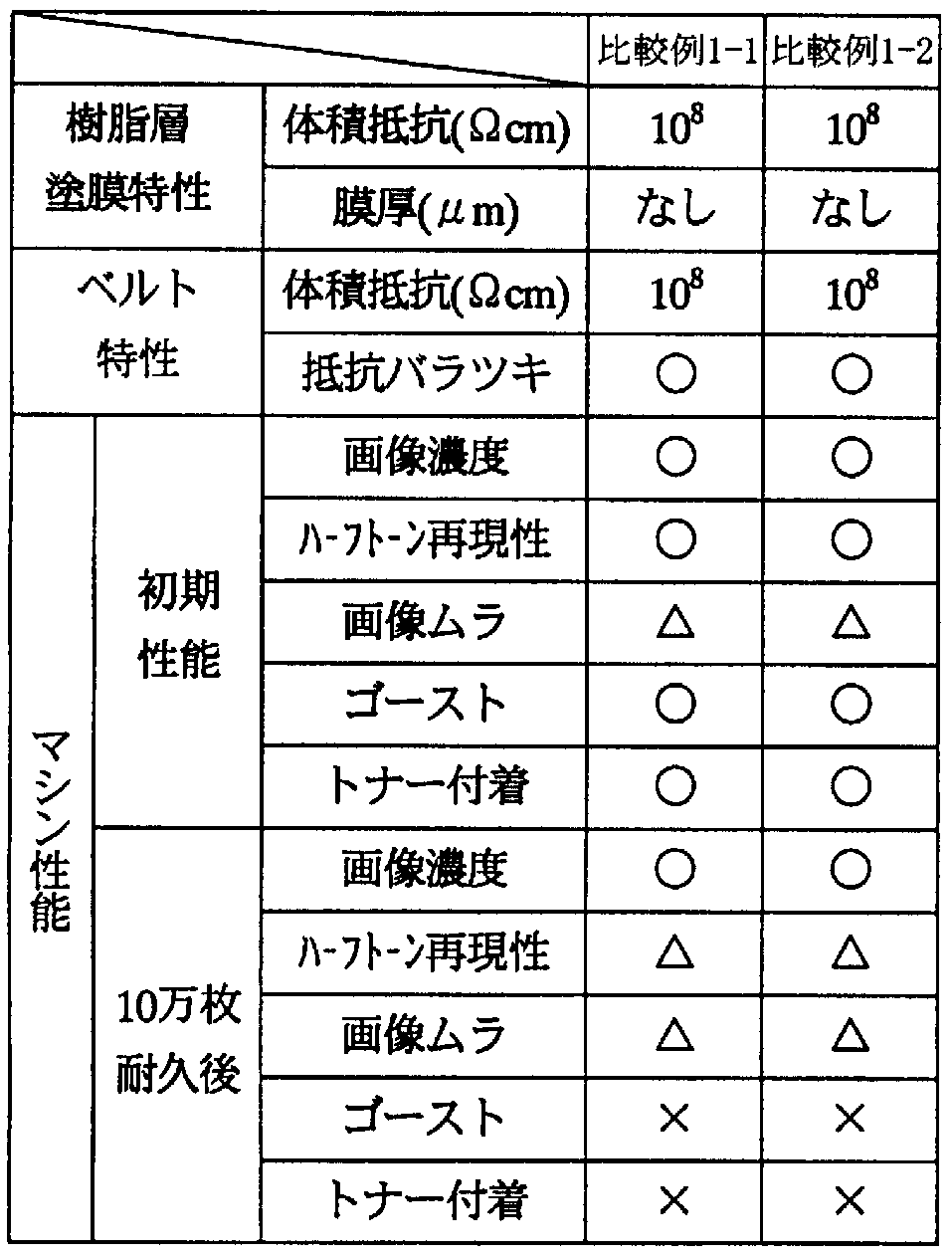
- Example 1 1 to 1 11, Comparative Example 1 1, 1-2
- Conductive endless belts of Examples and Comparative Examples were prepared with the formulations shown in Tables 6 to 8 below. Specifically, first, each compounding component of the belt base shown in each table is melt-kneaded with a twin-screw kneader, and the resulting kneaded product is extruded using an annular die. A belt substrate 101 having a thickness of 100 m and a width of 250 mm was produced. Thereafter, a non-solvent coating solution of the resin layer prepared using the compounding materials shown in each table on this belt substrate 101 was dried using a roll coater. : Coating was performed so that the value indicated in L1 was obtained.
- the base resin 5 - -
- PA12 Ube Industries, product name 3024U
- PET Product made by UCHIKA CORPORATION, trade name SA— 1206
- Carbon black manufactured by Denki Kagaku Kogyo Co., Ltd.
- Base resin Urethane acrylate oligomer, manufactured by Kyoeisha Chemical Co., Ltd., model number UF80 1
- Asilphosphine oxide manufactured by Ciba Specialty Chemicals, part number IRGAC URE819 (Maximum absorption wavelength: 430nm)
- the specific volume resistivity of the belt at a measurement voltage of 100V is used.
- the volume resistance of the resin layer was obtained by applying a coating solution on a copper plate and curing the coating film, and then measuring the resistance between the copper plate and the measurement electrode.
- the conductive endless belt of each example and comparative example and a metal drum were pressed against each other with a load of 500 g and rotated, and 100 V was applied between the belt and the drum to determine the maximum resistance within one belt circumference. The difference from the minimum resistance was determined to determine the resistance variation.
- Example 1-1 Example 1-2
- Example 1-3 Example 1-4
- Example 1-5 Example 1-6 mmm 10 13 10 13 10 10 10 8 10 10 10 6 Transfer characteristics ⁇ (" m) 2 2 30 10 10 5
- Belt 10 10 10 10 10 9
- Characteristic resistance variation ⁇ ⁇ ⁇ ⁇ ⁇ Image » ⁇ ⁇ ⁇ ⁇ ⁇ ⁇ Hafton reproducibility ⁇ ⁇ ⁇ ⁇ ⁇ Initial ⁇ Image irregularity ⁇ ⁇ ⁇ ⁇ ⁇ ⁇ Performance
- Example 1-7 Example 1-8 Example 1-9 Example 10 Example 1 -11 Picking 10 2 10 9 10 6 10 6 10 6
- Conductive endless belts of Examples and Comparative Examples were prepared with the formulations shown in Tables 12 to 14 below. Specifically, first, each compounding component of the belt base shown in each table is melt-kneaded with a twin-screw kneader, and the resulting kneaded product is extruded using an annular die. A belt substrate 101 having a thickness of 100 m and a width of 250 mm was produced. Thereafter, a solvent-free coating solution for the resin layer prepared using the compounding materials shown in each table on this belt substrate 101, using a roll coater, the film thickness after drying is as shown in Tables 12 to 12 below. Coating was performed so that the value shown in 14 was obtained.
- the conductive endless belt 100 was obtained by irradiating with an electron beam and curing the coating film of the resin layer 102.
- the resin layer 102 was not provided.
- Base resin 5 50 50 50 50 50 50 50 50 reactive (1) 50 50 50 50 50 50 dilute (2) - A - A - A
- PA12 Ube Industries, product name 3024U
- PET Product made by Unitika Ltd., trade name SA— 1206
- Carbon black manufactured by Denki Kagaku Kogyo Co., Ltd., trade name Denki Black
- Base resin Urethane acrylate oligomer, manufactured by Kyoeisha Chemical Co., Ltd., model number UV32 0
- the specific volume resistivity of the belt at a measurement voltage of 100V is used.
- the volume resistance of the resin layer was obtained by applying a coating solution on a copper plate and curing the coating film, and then measuring the resistance between the copper plate and the measurement electrode.
- the conductive endless belt of each example and comparative example and a metal drum were pressed against each other with a load of 500 g and rotated, and 100 V was applied between the belt and the drum to determine the maximum resistance within one belt circumference. The difference from the minimum resistance was determined to determine the resistance variation.
- Example 2-1 Example 2-2 Example 2-3
- Example 2-4 Example 2-5
- Example 2-6 Building roll resistance ( ⁇ ) 10 13 10 13 10 10 10 8 10 10 10 5
Landscapes
- Physics & Mathematics (AREA)
- General Physics & Mathematics (AREA)
- Engineering & Computer Science (AREA)
- Mechanical Engineering (AREA)
- Electrostatic Charge, Transfer And Separation In Electrography (AREA)
Abstract
Description




Claims
Priority Applications (1)
| Application Number | Priority Date | Filing Date | Title |
|---|---|---|---|
| US11/722,842 US7809315B2 (en) | 2004-12-28 | 2005-12-14 | Transfer/transport conductive endless belt for a tandem system, method for producing same, and image forming apparatus employing same |
Applications Claiming Priority (4)
| Application Number | Priority Date | Filing Date | Title |
|---|---|---|---|
| JP2004380912A JP2006184786A (ja) | 2004-12-28 | 2004-12-28 | 導電性エンドレスベルト、その製造方法およびそれを用いた画像形成装置 |
| JP2004-380911 | 2004-12-28 | ||
| JP2004-380912 | 2004-12-28 | ||
| JP2004380911A JP2006184785A (ja) | 2004-12-28 | 2004-12-28 | 導電性エンドレスベルト、その製造方法およびそれを用いた画像形成装置 |
Publications (1)
| Publication Number | Publication Date |
|---|---|
| WO2006070602A1 true WO2006070602A1 (ja) | 2006-07-06 |
Family
ID=36614722
Family Applications (1)
| Application Number | Title | Priority Date | Filing Date |
|---|---|---|---|
| PCT/JP2005/022977 Ceased WO2006070602A1 (ja) | 2004-12-28 | 2005-12-14 | 導電性エンドレスベルト、その製造方法およびそれを用いた画像形成装置 |
Country Status (2)
| Country | Link |
|---|---|
| US (1) | US7809315B2 (ja) |
| WO (1) | WO2006070602A1 (ja) |
Families Citing this family (316)
| Publication number | Priority date | Publication date | Assignee | Title |
|---|---|---|---|---|
| JP4942119B2 (ja) * | 2008-01-25 | 2012-05-30 | 株式会社ブリヂストン | 導電性エンドレスベルト |
| US9394608B2 (en) | 2009-04-06 | 2016-07-19 | Asm America, Inc. | Semiconductor processing reactor and components thereof |
| US8802201B2 (en) | 2009-08-14 | 2014-08-12 | Asm America, Inc. | Systems and methods for thin-film deposition of metal oxides using excited nitrogen-oxygen species |
| JP5632396B2 (ja) * | 2010-02-04 | 2014-11-26 | 株式会社ブリヂストン | 導電性エンドレスベルト |
| US8417163B2 (en) * | 2010-02-12 | 2013-04-09 | Fuji Xerox Co., Ltd. | Resin material, endless belt for image forming apparatus, roller for image forming apparatus, image fixing device, and image forming apparatus |
| US8540900B2 (en) * | 2010-03-25 | 2013-09-24 | Xerox Corporation | Intermediate transfer belts |
| US9017772B2 (en) * | 2010-07-08 | 2015-04-28 | Xerox Corporation | Process for fabrication of seamless UV cured intermediate transfer belts (ITB) |
| US20130023129A1 (en) | 2011-07-20 | 2013-01-24 | Asm America, Inc. | Pressure transmitter for a semiconductor processing environment |
| US9017481B1 (en) | 2011-10-28 | 2015-04-28 | Asm America, Inc. | Process feed management for semiconductor substrate processing |
| US10714315B2 (en) | 2012-10-12 | 2020-07-14 | Asm Ip Holdings B.V. | Semiconductor reaction chamber showerhead |
| US20160376700A1 (en) | 2013-02-01 | 2016-12-29 | Asm Ip Holding B.V. | System for treatment of deposition reactor |
| JP5821884B2 (ja) * | 2013-03-25 | 2015-11-24 | コニカミノルタ株式会社 | 転写部材および画像形成装置 |
| US11015245B2 (en) | 2014-03-19 | 2021-05-25 | Asm Ip Holding B.V. | Gas-phase reactor and system having exhaust plenum and components thereof |
| US10858737B2 (en) | 2014-07-28 | 2020-12-08 | Asm Ip Holding B.V. | Showerhead assembly and components thereof |
| US9890456B2 (en) | 2014-08-21 | 2018-02-13 | Asm Ip Holding B.V. | Method and system for in situ formation of gas-phase compounds |
| US10941490B2 (en) | 2014-10-07 | 2021-03-09 | Asm Ip Holding B.V. | Multiple temperature range susceptor, assembly, reactor and system including the susceptor, and methods of using the same |
| US10276355B2 (en) | 2015-03-12 | 2019-04-30 | Asm Ip Holding B.V. | Multi-zone reactor, system including the reactor, and method of using the same |
| US10458018B2 (en) | 2015-06-26 | 2019-10-29 | Asm Ip Holding B.V. | Structures including metal carbide material, devices including the structures, and methods of forming same |
| US10211308B2 (en) | 2015-10-21 | 2019-02-19 | Asm Ip Holding B.V. | NbMC layers |
| US11139308B2 (en) | 2015-12-29 | 2021-10-05 | Asm Ip Holding B.V. | Atomic layer deposition of III-V compounds to form V-NAND devices |
| US10529554B2 (en) | 2016-02-19 | 2020-01-07 | Asm Ip Holding B.V. | Method for forming silicon nitride film selectively on sidewalls or flat surfaces of trenches |
| US10343920B2 (en) | 2016-03-18 | 2019-07-09 | Asm Ip Holding B.V. | Aligned carbon nanotubes |
| US10190213B2 (en) | 2016-04-21 | 2019-01-29 | Asm Ip Holding B.V. | Deposition of metal borides |
| US10865475B2 (en) | 2016-04-21 | 2020-12-15 | Asm Ip Holding B.V. | Deposition of metal borides and silicides |
| US10367080B2 (en) | 2016-05-02 | 2019-07-30 | Asm Ip Holding B.V. | Method of forming a germanium oxynitride film |
| US11453943B2 (en) | 2016-05-25 | 2022-09-27 | Asm Ip Holding B.V. | Method for forming carbon-containing silicon/metal oxide or nitride film by ALD using silicon precursor and hydrocarbon precursor |
| US10612137B2 (en) | 2016-07-08 | 2020-04-07 | Asm Ip Holdings B.V. | Organic reactants for atomic layer deposition |
| US9859151B1 (en) | 2016-07-08 | 2018-01-02 | Asm Ip Holding B.V. | Selective film deposition method to form air gaps |
| US10714385B2 (en) | 2016-07-19 | 2020-07-14 | Asm Ip Holding B.V. | Selective deposition of tungsten |
| US9887082B1 (en) | 2016-07-28 | 2018-02-06 | Asm Ip Holding B.V. | Method and apparatus for filling a gap |
| US9812320B1 (en) | 2016-07-28 | 2017-11-07 | Asm Ip Holding B.V. | Method and apparatus for filling a gap |
| KR102532607B1 (ko) | 2016-07-28 | 2023-05-15 | 에이에스엠 아이피 홀딩 비.브이. | 기판 가공 장치 및 그 동작 방법 |
| US10643826B2 (en) | 2016-10-26 | 2020-05-05 | Asm Ip Holdings B.V. | Methods for thermally calibrating reaction chambers |
| US11532757B2 (en) | 2016-10-27 | 2022-12-20 | Asm Ip Holding B.V. | Deposition of charge trapping layers |
| US10229833B2 (en) | 2016-11-01 | 2019-03-12 | Asm Ip Holding B.V. | Methods for forming a transition metal nitride film on a substrate by atomic layer deposition and related semiconductor device structures |
| US10714350B2 (en) | 2016-11-01 | 2020-07-14 | ASM IP Holdings, B.V. | Methods for forming a transition metal niobium nitride film on a substrate by atomic layer deposition and related semiconductor device structures |
| KR102546317B1 (ko) | 2016-11-15 | 2023-06-21 | 에이에스엠 아이피 홀딩 비.브이. | 기체 공급 유닛 및 이를 포함하는 기판 처리 장치 |
| KR102762543B1 (ko) | 2016-12-14 | 2025-02-05 | 에이에스엠 아이피 홀딩 비.브이. | 기판 처리 장치 |
| US11581186B2 (en) | 2016-12-15 | 2023-02-14 | Asm Ip Holding B.V. | Sequential infiltration synthesis apparatus |
| US11447861B2 (en) | 2016-12-15 | 2022-09-20 | Asm Ip Holding B.V. | Sequential infiltration synthesis apparatus and a method of forming a patterned structure |
| KR102700194B1 (ko) | 2016-12-19 | 2024-08-28 | 에이에스엠 아이피 홀딩 비.브이. | 기판 처리 장치 |
| US10269558B2 (en) | 2016-12-22 | 2019-04-23 | Asm Ip Holding B.V. | Method of forming a structure on a substrate |
| US10867788B2 (en) | 2016-12-28 | 2020-12-15 | Asm Ip Holding B.V. | Method of forming a structure on a substrate |
| US11390950B2 (en) | 2017-01-10 | 2022-07-19 | Asm Ip Holding B.V. | Reactor system and method to reduce residue buildup during a film deposition process |
| US10468261B2 (en) | 2017-02-15 | 2019-11-05 | Asm Ip Holding B.V. | Methods for forming a metallic film on a substrate by cyclical deposition and related semiconductor device structures |
| US10529563B2 (en) | 2017-03-29 | 2020-01-07 | Asm Ip Holdings B.V. | Method for forming doped metal oxide films on a substrate by cyclical deposition and related semiconductor device structures |
| KR102457289B1 (ko) | 2017-04-25 | 2022-10-21 | 에이에스엠 아이피 홀딩 비.브이. | 박막 증착 방법 및 반도체 장치의 제조 방법 |
| US10770286B2 (en) | 2017-05-08 | 2020-09-08 | Asm Ip Holdings B.V. | Methods for selectively forming a silicon nitride film on a substrate and related semiconductor device structures |
| US10892156B2 (en) | 2017-05-08 | 2021-01-12 | Asm Ip Holding B.V. | Methods for forming a silicon nitride film on a substrate and related semiconductor device structures |
| US10886123B2 (en) | 2017-06-02 | 2021-01-05 | Asm Ip Holding B.V. | Methods for forming low temperature semiconductor layers and related semiconductor device structures |
| US12040200B2 (en) | 2017-06-20 | 2024-07-16 | Asm Ip Holding B.V. | Semiconductor processing apparatus and methods for calibrating a semiconductor processing apparatus |
| US11306395B2 (en) | 2017-06-28 | 2022-04-19 | Asm Ip Holding B.V. | Methods for depositing a transition metal nitride film on a substrate by atomic layer deposition and related deposition apparatus |
| US10685834B2 (en) | 2017-07-05 | 2020-06-16 | Asm Ip Holdings B.V. | Methods for forming a silicon germanium tin layer and related semiconductor device structures |
| KR20190009245A (ko) | 2017-07-18 | 2019-01-28 | 에이에스엠 아이피 홀딩 비.브이. | 반도체 소자 구조물 형성 방법 및 관련된 반도체 소자 구조물 |
| US11374112B2 (en) | 2017-07-19 | 2022-06-28 | Asm Ip Holding B.V. | Method for depositing a group IV semiconductor and related semiconductor device structures |
| US10541333B2 (en) | 2017-07-19 | 2020-01-21 | Asm Ip Holding B.V. | Method for depositing a group IV semiconductor and related semiconductor device structures |
| US11018002B2 (en) | 2017-07-19 | 2021-05-25 | Asm Ip Holding B.V. | Method for selectively depositing a Group IV semiconductor and related semiconductor device structures |
| US10590535B2 (en) | 2017-07-26 | 2020-03-17 | Asm Ip Holdings B.V. | Chemical treatment, deposition and/or infiltration apparatus and method for using the same |
| TWI815813B (zh) | 2017-08-04 | 2023-09-21 | 荷蘭商Asm智慧財產控股公司 | 用於分配反應腔內氣體的噴頭總成 |
| US10692741B2 (en) | 2017-08-08 | 2020-06-23 | Asm Ip Holdings B.V. | Radiation shield |
| US10770336B2 (en) | 2017-08-08 | 2020-09-08 | Asm Ip Holding B.V. | Substrate lift mechanism and reactor including same |
| US11769682B2 (en) | 2017-08-09 | 2023-09-26 | Asm Ip Holding B.V. | Storage apparatus for storing cassettes for substrates and processing apparatus equipped therewith |
| US11139191B2 (en) | 2017-08-09 | 2021-10-05 | Asm Ip Holding B.V. | Storage apparatus for storing cassettes for substrates and processing apparatus equipped therewith |
| US11830730B2 (en) | 2017-08-29 | 2023-11-28 | Asm Ip Holding B.V. | Layer forming method and apparatus |
| KR102491945B1 (ko) | 2017-08-30 | 2023-01-26 | 에이에스엠 아이피 홀딩 비.브이. | 기판 처리 장치 |
| US11056344B2 (en) | 2017-08-30 | 2021-07-06 | Asm Ip Holding B.V. | Layer forming method |
| US11295980B2 (en) | 2017-08-30 | 2022-04-05 | Asm Ip Holding B.V. | Methods for depositing a molybdenum metal film over a dielectric surface of a substrate by a cyclical deposition process and related semiconductor device structures |
| KR102401446B1 (ko) | 2017-08-31 | 2022-05-24 | 에이에스엠 아이피 홀딩 비.브이. | 기판 처리 장치 |
| KR102630301B1 (ko) | 2017-09-21 | 2024-01-29 | 에이에스엠 아이피 홀딩 비.브이. | 침투성 재료의 순차 침투 합성 방법 처리 및 이를 이용하여 형성된 구조물 및 장치 |
| US10844484B2 (en) | 2017-09-22 | 2020-11-24 | Asm Ip Holding B.V. | Apparatus for dispensing a vapor phase reactant to a reaction chamber and related methods |
| US10658205B2 (en) | 2017-09-28 | 2020-05-19 | Asm Ip Holdings B.V. | Chemical dispensing apparatus and methods for dispensing a chemical to a reaction chamber |
| US10403504B2 (en) | 2017-10-05 | 2019-09-03 | Asm Ip Holding B.V. | Method for selectively depositing a metallic film on a substrate |
| US10319588B2 (en) | 2017-10-10 | 2019-06-11 | Asm Ip Holding B.V. | Method for depositing a metal chalcogenide on a substrate by cyclical deposition |
| US10923344B2 (en) | 2017-10-30 | 2021-02-16 | Asm Ip Holding B.V. | Methods for forming a semiconductor structure and related semiconductor structures |
| US10910262B2 (en) | 2017-11-16 | 2021-02-02 | Asm Ip Holding B.V. | Method of selectively depositing a capping layer structure on a semiconductor device structure |
| US11022879B2 (en) | 2017-11-24 | 2021-06-01 | Asm Ip Holding B.V. | Method of forming an enhanced unexposed photoresist layer |
| JP7214724B2 (ja) | 2017-11-27 | 2023-01-30 | エーエスエム アイピー ホールディング ビー.ブイ. | バッチ炉で利用されるウェハカセットを収納するための収納装置 |
| TWI791689B (zh) | 2017-11-27 | 2023-02-11 | 荷蘭商Asm智慧財產控股私人有限公司 | 包括潔淨迷你環境之裝置 |
| US10872771B2 (en) | 2018-01-16 | 2020-12-22 | Asm Ip Holding B. V. | Method for depositing a material film on a substrate within a reaction chamber by a cyclical deposition process and related device structures |
| TWI799494B (zh) | 2018-01-19 | 2023-04-21 | 荷蘭商Asm 智慧財產控股公司 | 沈積方法 |
| KR102695659B1 (ko) | 2018-01-19 | 2024-08-14 | 에이에스엠 아이피 홀딩 비.브이. | 플라즈마 보조 증착에 의해 갭 충진 층을 증착하는 방법 |
| US11018047B2 (en) | 2018-01-25 | 2021-05-25 | Asm Ip Holding B.V. | Hybrid lift pin |
| USD880437S1 (en) | 2018-02-01 | 2020-04-07 | Asm Ip Holding B.V. | Gas supply plate for semiconductor manufacturing apparatus |
| US11081345B2 (en) | 2018-02-06 | 2021-08-03 | Asm Ip Holding B.V. | Method of post-deposition treatment for silicon oxide film |
| US11685991B2 (en) | 2018-02-14 | 2023-06-27 | Asm Ip Holding B.V. | Method for depositing a ruthenium-containing film on a substrate by a cyclical deposition process |
| US10896820B2 (en) | 2018-02-14 | 2021-01-19 | Asm Ip Holding B.V. | Method for depositing a ruthenium-containing film on a substrate by a cyclical deposition process |
| US10731249B2 (en) | 2018-02-15 | 2020-08-04 | Asm Ip Holding B.V. | Method of forming a transition metal containing film on a substrate by a cyclical deposition process, a method for supplying a transition metal halide compound to a reaction chamber, and related vapor deposition apparatus |
| KR102636427B1 (ko) | 2018-02-20 | 2024-02-13 | 에이에스엠 아이피 홀딩 비.브이. | 기판 처리 방법 및 장치 |
| US10975470B2 (en) | 2018-02-23 | 2021-04-13 | Asm Ip Holding B.V. | Apparatus for detecting or monitoring for a chemical precursor in a high temperature environment |
| JP7006377B2 (ja) * | 2018-02-28 | 2022-01-24 | コニカミノルタ株式会社 | 中間転写ベルト及び画像形成装置 |
| US11473195B2 (en) | 2018-03-01 | 2022-10-18 | Asm Ip Holding B.V. | Semiconductor processing apparatus and a method for processing a substrate |
| US11629406B2 (en) | 2018-03-09 | 2023-04-18 | Asm Ip Holding B.V. | Semiconductor processing apparatus comprising one or more pyrometers for measuring a temperature of a substrate during transfer of the substrate |
| US11114283B2 (en) | 2018-03-16 | 2021-09-07 | Asm Ip Holding B.V. | Reactor, system including the reactor, and methods of manufacturing and using same |
| KR102646467B1 (ko) | 2018-03-27 | 2024-03-11 | 에이에스엠 아이피 홀딩 비.브이. | 기판 상에 전극을 형성하는 방법 및 전극을 포함하는 반도체 소자 구조 |
| US11230766B2 (en) | 2018-03-29 | 2022-01-25 | Asm Ip Holding B.V. | Substrate processing apparatus and method |
| US11088002B2 (en) | 2018-03-29 | 2021-08-10 | Asm Ip Holding B.V. | Substrate rack and a substrate processing system and method |
| KR102501472B1 (ko) | 2018-03-30 | 2023-02-20 | 에이에스엠 아이피 홀딩 비.브이. | 기판 처리 방법 |
| KR102600229B1 (ko) | 2018-04-09 | 2023-11-10 | 에이에스엠 아이피 홀딩 비.브이. | 기판 지지 장치, 이를 포함하는 기판 처리 장치 및 기판 처리 방법 |
| US12025484B2 (en) | 2018-05-08 | 2024-07-02 | Asm Ip Holding B.V. | Thin film forming method |
| TWI843623B (zh) | 2018-05-08 | 2024-05-21 | 荷蘭商Asm Ip私人控股有限公司 | 藉由循環沉積製程於基板上沉積氧化物膜之方法及相關裝置結構 |
| US12272527B2 (en) | 2018-05-09 | 2025-04-08 | Asm Ip Holding B.V. | Apparatus for use with hydrogen radicals and method of using same |
| KR20190129718A (ko) | 2018-05-11 | 2019-11-20 | 에이에스엠 아이피 홀딩 비.브이. | 기판 상에 피도핑 금속 탄화물 막을 형성하는 방법 및 관련 반도체 소자 구조 |
| KR102596988B1 (ko) | 2018-05-28 | 2023-10-31 | 에이에스엠 아이피 홀딩 비.브이. | 기판 처리 방법 및 그에 의해 제조된 장치 |
| TWI840362B (zh) | 2018-06-04 | 2024-05-01 | 荷蘭商Asm Ip私人控股有限公司 | 水氣降低的晶圓處置腔室 |
| US11718913B2 (en) | 2018-06-04 | 2023-08-08 | Asm Ip Holding B.V. | Gas distribution system and reactor system including same |
| US11286562B2 (en) | 2018-06-08 | 2022-03-29 | Asm Ip Holding B.V. | Gas-phase chemical reactor and method of using same |
| KR102568797B1 (ko) | 2018-06-21 | 2023-08-21 | 에이에스엠 아이피 홀딩 비.브이. | 기판 처리 시스템 |
| US10797133B2 (en) | 2018-06-21 | 2020-10-06 | Asm Ip Holding B.V. | Method for depositing a phosphorus doped silicon arsenide film and related semiconductor device structures |
| TWI871083B (zh) | 2018-06-27 | 2025-01-21 | 荷蘭商Asm Ip私人控股有限公司 | 用於形成含金屬材料之循環沉積製程 |
| US11499222B2 (en) | 2018-06-27 | 2022-11-15 | Asm Ip Holding B.V. | Cyclic deposition methods for forming metal-containing material and films and structures including the metal-containing material |
| KR102686758B1 (ko) | 2018-06-29 | 2024-07-18 | 에이에스엠 아이피 홀딩 비.브이. | 박막 증착 방법 및 반도체 장치의 제조 방법 |
| US10612136B2 (en) | 2018-06-29 | 2020-04-07 | ASM IP Holding, B.V. | Temperature-controlled flange and reactor system including same |
| US10755922B2 (en) * | 2018-07-03 | 2020-08-25 | Asm Ip Holding B.V. | Method for depositing silicon-free carbon-containing film as gap-fill layer by pulse plasma-assisted deposition |
| US10388513B1 (en) * | 2018-07-03 | 2019-08-20 | Asm Ip Holding B.V. | Method for depositing silicon-free carbon-containing film as gap-fill layer by pulse plasma-assisted deposition |
| US10767789B2 (en) | 2018-07-16 | 2020-09-08 | Asm Ip Holding B.V. | Diaphragm valves, valve components, and methods for forming valve components |
| US11053591B2 (en) | 2018-08-06 | 2021-07-06 | Asm Ip Holding B.V. | Multi-port gas injection system and reactor system including same |
| US10883175B2 (en) | 2018-08-09 | 2021-01-05 | Asm Ip Holding B.V. | Vertical furnace for processing substrates and a liner for use therein |
| US10829852B2 (en) | 2018-08-16 | 2020-11-10 | Asm Ip Holding B.V. | Gas distribution device for a wafer processing apparatus |
| US11430674B2 (en) | 2018-08-22 | 2022-08-30 | Asm Ip Holding B.V. | Sensor array, apparatus for dispensing a vapor phase reactant to a reaction chamber and related methods |
| US11024523B2 (en) | 2018-09-11 | 2021-06-01 | Asm Ip Holding B.V. | Substrate processing apparatus and method |
| KR102707956B1 (ko) | 2018-09-11 | 2024-09-19 | 에이에스엠 아이피 홀딩 비.브이. | 박막 증착 방법 |
| US11049751B2 (en) | 2018-09-14 | 2021-06-29 | Asm Ip Holding B.V. | Cassette supply system to store and handle cassettes and processing apparatus equipped therewith |
| CN110970344B (zh) | 2018-10-01 | 2024-10-25 | Asmip控股有限公司 | 衬底保持设备、包含所述设备的系统及其使用方法 |
| US11232963B2 (en) | 2018-10-03 | 2022-01-25 | Asm Ip Holding B.V. | Substrate processing apparatus and method |
| KR102592699B1 (ko) | 2018-10-08 | 2023-10-23 | 에이에스엠 아이피 홀딩 비.브이. | 기판 지지 유닛 및 이를 포함하는 박막 증착 장치와 기판 처리 장치 |
| US10847365B2 (en) | 2018-10-11 | 2020-11-24 | Asm Ip Holding B.V. | Method of forming conformal silicon carbide film by cyclic CVD |
| US10811256B2 (en) | 2018-10-16 | 2020-10-20 | Asm Ip Holding B.V. | Method for etching a carbon-containing feature |
| KR102546322B1 (ko) | 2018-10-19 | 2023-06-21 | 에이에스엠 아이피 홀딩 비.브이. | 기판 처리 장치 및 기판 처리 방법 |
| KR102605121B1 (ko) | 2018-10-19 | 2023-11-23 | 에이에스엠 아이피 홀딩 비.브이. | 기판 처리 장치 및 기판 처리 방법 |
| USD948463S1 (en) | 2018-10-24 | 2022-04-12 | Asm Ip Holding B.V. | Susceptor for semiconductor substrate supporting apparatus |
| US12378665B2 (en) | 2018-10-26 | 2025-08-05 | Asm Ip Holding B.V. | High temperature coatings for a preclean and etch apparatus and related methods |
| US11087997B2 (en) | 2018-10-31 | 2021-08-10 | Asm Ip Holding B.V. | Substrate processing apparatus for processing substrates |
| KR102748291B1 (ko) | 2018-11-02 | 2024-12-31 | 에이에스엠 아이피 홀딩 비.브이. | 기판 지지 유닛 및 이를 포함하는 기판 처리 장치 |
| US11572620B2 (en) | 2018-11-06 | 2023-02-07 | Asm Ip Holding B.V. | Methods for selectively depositing an amorphous silicon film on a substrate |
| US11031242B2 (en) | 2018-11-07 | 2021-06-08 | Asm Ip Holding B.V. | Methods for depositing a boron doped silicon germanium film |
| US10818758B2 (en) | 2018-11-16 | 2020-10-27 | Asm Ip Holding B.V. | Methods for forming a metal silicate film on a substrate in a reaction chamber and related semiconductor device structures |
| US10847366B2 (en) | 2018-11-16 | 2020-11-24 | Asm Ip Holding B.V. | Methods for depositing a transition metal chalcogenide film on a substrate by a cyclical deposition process |
| US12040199B2 (en) | 2018-11-28 | 2024-07-16 | Asm Ip Holding B.V. | Substrate processing apparatus for processing substrates |
| US11217444B2 (en) | 2018-11-30 | 2022-01-04 | Asm Ip Holding B.V. | Method for forming an ultraviolet radiation responsive metal oxide-containing film |
| KR102636428B1 (ko) | 2018-12-04 | 2024-02-13 | 에이에스엠 아이피 홀딩 비.브이. | 기판 처리 장치를 세정하는 방법 |
| US11158513B2 (en) | 2018-12-13 | 2021-10-26 | Asm Ip Holding B.V. | Methods for forming a rhenium-containing film on a substrate by a cyclical deposition process and related semiconductor device structures |
| JP7504584B2 (ja) | 2018-12-14 | 2024-06-24 | エーエスエム・アイピー・ホールディング・ベー・フェー | 窒化ガリウムの選択的堆積を用いてデバイス構造体を形成する方法及びそのためのシステム |
| TWI866480B (zh) | 2019-01-17 | 2024-12-11 | 荷蘭商Asm Ip 私人控股有限公司 | 藉由循環沈積製程於基板上形成含過渡金屬膜之方法 |
| KR102727227B1 (ko) | 2019-01-22 | 2024-11-07 | 에이에스엠 아이피 홀딩 비.브이. | 기판 처리 장치 |
| CN111524788B (zh) | 2019-02-01 | 2023-11-24 | Asm Ip私人控股有限公司 | 氧化硅的拓扑选择性膜形成的方法 |
| KR20200102357A (ko) | 2019-02-20 | 2020-08-31 | 에이에스엠 아이피 홀딩 비.브이. | 3-d nand 응용의 플러그 충진체 증착용 장치 및 방법 |
| TWI873122B (zh) | 2019-02-20 | 2025-02-21 | 荷蘭商Asm Ip私人控股有限公司 | 填充一基板之一表面內所形成的一凹槽的方法、根據其所形成之半導體結構、及半導體處理設備 |
| KR102626263B1 (ko) | 2019-02-20 | 2024-01-16 | 에이에스엠 아이피 홀딩 비.브이. | 처리 단계를 포함하는 주기적 증착 방법 및 이를 위한 장치 |
| TWI845607B (zh) | 2019-02-20 | 2024-06-21 | 荷蘭商Asm Ip私人控股有限公司 | 用來填充形成於基材表面內之凹部的循環沉積方法及設備 |
| TWI842826B (zh) | 2019-02-22 | 2024-05-21 | 荷蘭商Asm Ip私人控股有限公司 | 基材處理設備及處理基材之方法 |
| KR102782593B1 (ko) | 2019-03-08 | 2025-03-14 | 에이에스엠 아이피 홀딩 비.브이. | SiOC 층을 포함한 구조체 및 이의 형성 방법 |
| KR102858005B1 (ko) | 2019-03-08 | 2025-09-09 | 에이에스엠 아이피 홀딩 비.브이. | 실리콘 질화물 층을 선택적으로 증착하는 방법, 및 선택적으로 증착된 실리콘 질화물 층을 포함하는 구조체 |
| KR102762833B1 (ko) | 2019-03-08 | 2025-02-04 | 에이에스엠 아이피 홀딩 비.브이. | SiOCN 층을 포함한 구조체 및 이의 형성 방법 |
| JP2020167398A (ja) | 2019-03-28 | 2020-10-08 | エーエスエム・アイピー・ホールディング・ベー・フェー | ドアオープナーおよびドアオープナーが提供される基材処理装置 |
| KR102809999B1 (ko) | 2019-04-01 | 2025-05-19 | 에이에스엠 아이피 홀딩 비.브이. | 반도체 소자를 제조하는 방법 |
| KR102897355B1 (ko) | 2019-04-19 | 2025-12-08 | 에이에스엠 아이피 홀딩 비.브이. | 층 형성 방법 및 장치 |
| KR20200125453A (ko) | 2019-04-24 | 2020-11-04 | 에이에스엠 아이피 홀딩 비.브이. | 기상 반응기 시스템 및 이를 사용하는 방법 |
| KR102869364B1 (ko) | 2019-05-07 | 2025-10-10 | 에이에스엠 아이피 홀딩 비.브이. | 비정질 탄소 중합체 막을 개질하는 방법 |
| KR102929471B1 (ko) | 2019-05-07 | 2026-02-20 | 에이에스엠 아이피 홀딩 비.브이. | 딥 튜브가 있는 화학물질 공급원 용기 |
| KR102929472B1 (ko) | 2019-05-10 | 2026-02-20 | 에이에스엠 아이피 홀딩 비.브이. | 표면 상에 재료를 증착하는 방법 및 본 방법에 따라 형성된 구조 |
| JP7612342B2 (ja) | 2019-05-16 | 2025-01-14 | エーエスエム・アイピー・ホールディング・ベー・フェー | ウェハボートハンドリング装置、縦型バッチ炉および方法 |
| JP7598201B2 (ja) | 2019-05-16 | 2024-12-11 | エーエスエム・アイピー・ホールディング・ベー・フェー | ウェハボートハンドリング装置、縦型バッチ炉および方法 |
| USD975665S1 (en) | 2019-05-17 | 2023-01-17 | Asm Ip Holding B.V. | Susceptor shaft |
| USD947913S1 (en) | 2019-05-17 | 2022-04-05 | Asm Ip Holding B.V. | Susceptor shaft |
| USD935572S1 (en) | 2019-05-24 | 2021-11-09 | Asm Ip Holding B.V. | Gas channel plate |
| USD922229S1 (en) | 2019-06-05 | 2021-06-15 | Asm Ip Holding B.V. | Device for controlling a temperature of a gas supply unit |
| KR20200141002A (ko) | 2019-06-06 | 2020-12-17 | 에이에스엠 아이피 홀딩 비.브이. | 배기 가스 분석을 포함한 기상 반응기 시스템을 사용하는 방법 |
| KR102918757B1 (ko) | 2019-06-10 | 2026-01-28 | 에이에스엠 아이피 홀딩 비.브이. | 석영 에피택셜 챔버를 세정하는 방법 |
| KR20200143254A (ko) | 2019-06-11 | 2020-12-23 | 에이에스엠 아이피 홀딩 비.브이. | 개질 가스를 사용하여 전자 구조를 형성하는 방법, 상기 방법을 수행하기 위한 시스템, 및 상기 방법을 사용하여 형성되는 구조 |
| USD944946S1 (en) | 2019-06-14 | 2022-03-01 | Asm Ip Holding B.V. | Shower plate |
| USD931978S1 (en) | 2019-06-27 | 2021-09-28 | Asm Ip Holding B.V. | Showerhead vacuum transport |
| KR102911421B1 (ko) | 2019-07-03 | 2026-01-12 | 에이에스엠 아이피 홀딩 비.브이. | 기판 처리 장치용 온도 제어 조립체 및 이를 사용하는 방법 |
| JP7499079B2 (ja) | 2019-07-09 | 2024-06-13 | エーエスエム・アイピー・ホールディング・ベー・フェー | 同軸導波管を用いたプラズマ装置、基板処理方法 |
| CN112216646B (zh) | 2019-07-10 | 2026-02-10 | Asmip私人控股有限公司 | 基板支撑组件及包括其的基板处理装置 |
| KR102895115B1 (ko) | 2019-07-16 | 2025-12-03 | 에이에스엠 아이피 홀딩 비.브이. | 기판 처리 장치 |
| TWI826704B (zh) | 2019-07-17 | 2023-12-21 | 荷蘭商Asm Ip私人控股有限公司 | 自由基輔助引燃電漿系統和方法 |
| KR102860110B1 (ko) | 2019-07-17 | 2025-09-16 | 에이에스엠 아이피 홀딩 비.브이. | 실리콘 게르마늄 구조를 형성하는 방법 |
| US11643724B2 (en) | 2019-07-18 | 2023-05-09 | Asm Ip Holding B.V. | Method of forming structures using a neutral beam |
| TWI839544B (zh) | 2019-07-19 | 2024-04-21 | 荷蘭商Asm Ip私人控股有限公司 | 形成形貌受控的非晶碳聚合物膜之方法 |
| KR102903090B1 (ko) | 2019-07-19 | 2025-12-19 | 에이에스엠 아이피 홀딩 비.브이. | 토폴로지-제어된 비정질 탄소 중합체 막을 형성하는 방법 |
| CN112309843B (zh) | 2019-07-29 | 2026-01-23 | Asmip私人控股有限公司 | 实现高掺杂剂掺入的选择性沉积方法 |
| CN112309900B (zh) | 2019-07-30 | 2025-11-04 | Asmip私人控股有限公司 | 基板处理设备 |
| CN112309899B (zh) | 2019-07-30 | 2025-11-14 | Asmip私人控股有限公司 | 基板处理设备 |
| KR20210015655A (ko) | 2019-07-30 | 2021-02-10 | 에이에스엠 아이피 홀딩 비.브이. | 기판 처리 장치 및 방법 |
| US11227782B2 (en) | 2019-07-31 | 2022-01-18 | Asm Ip Holding B.V. | Vertical batch furnace assembly |
| US11587815B2 (en) | 2019-07-31 | 2023-02-21 | Asm Ip Holding B.V. | Vertical batch furnace assembly |
| US11587814B2 (en) | 2019-07-31 | 2023-02-21 | Asm Ip Holding B.V. | Vertical batch furnace assembly |
| KR20210018759A (ko) | 2019-08-05 | 2021-02-18 | 에이에스엠 아이피 홀딩 비.브이. | 화학물질 공급원 용기를 위한 액체 레벨 센서 |
| KR20210018761A (ko) | 2019-08-09 | 2021-02-18 | 에이에스엠 아이피 홀딩 비.브이. | 냉각 장치를 포함한 히터 어셈블리 및 이를 사용하는 방법 |
| USD965044S1 (en) | 2019-08-19 | 2022-09-27 | Asm Ip Holding B.V. | Susceptor shaft |
| USD965524S1 (en) | 2019-08-19 | 2022-10-04 | Asm Ip Holding B.V. | Susceptor support |
| JP7810514B2 (ja) | 2019-08-21 | 2026-02-03 | エーエスエム・アイピー・ホールディング・ベー・フェー | 成膜原料混合ガス生成装置及び成膜装置 |
| USD940837S1 (en) | 2019-08-22 | 2022-01-11 | Asm Ip Holding B.V. | Electrode |
| USD979506S1 (en) | 2019-08-22 | 2023-02-28 | Asm Ip Holding B.V. | Insulator |
| USD930782S1 (en) | 2019-08-22 | 2021-09-14 | Asm Ip Holding B.V. | Gas distributor |
| USD949319S1 (en) | 2019-08-22 | 2022-04-19 | Asm Ip Holding B.V. | Exhaust duct |
| KR20210024423A (ko) | 2019-08-22 | 2021-03-05 | 에이에스엠 아이피 홀딩 비.브이. | 홀을 구비한 구조체를 형성하기 위한 방법 |
| US11286558B2 (en) | 2019-08-23 | 2022-03-29 | Asm Ip Holding B.V. | Methods for depositing a molybdenum nitride film on a surface of a substrate by a cyclical deposition process and related semiconductor device structures including a molybdenum nitride film |
| KR102928101B1 (ko) | 2019-08-23 | 2026-02-13 | 에이에스엠 아이피 홀딩 비.브이. | 비스(디에틸아미노)실란을 사용하여 peald에 의해 개선된 품질을 갖는 실리콘 산화물 막을 증착하기 위한 방법 |
| KR102868968B1 (ko) | 2019-09-03 | 2025-10-10 | 에이에스엠 아이피 홀딩 비.브이. | 칼코지나이드 막 및 상기 막을 포함한 구조체를 증착하기 위한 방법 및 장치 |
| KR102806450B1 (ko) | 2019-09-04 | 2025-05-12 | 에이에스엠 아이피 홀딩 비.브이. | 희생 캡핑 층을 이용한 선택적 증착 방법 |
| KR102733104B1 (ko) | 2019-09-05 | 2024-11-22 | 에이에스엠 아이피 홀딩 비.브이. | 기판 처리 장치 |
| US12469693B2 (en) | 2019-09-17 | 2025-11-11 | Asm Ip Holding B.V. | Method of forming a carbon-containing layer and structure including the layer |
| US11562901B2 (en) | 2019-09-25 | 2023-01-24 | Asm Ip Holding B.V. | Substrate processing method |
| CN112593212B (zh) | 2019-10-02 | 2023-12-22 | Asm Ip私人控股有限公司 | 通过循环等离子体增强沉积工艺形成拓扑选择性氧化硅膜的方法 |
| TWI846953B (zh) | 2019-10-08 | 2024-07-01 | 荷蘭商Asm Ip私人控股有限公司 | 基板處理裝置 |
| KR102948143B1 (ko) | 2019-10-08 | 2026-04-07 | 에이에스엠 아이피 홀딩 비.브이. | 활성 종을 이용하기 위한 가스 분배 어셈블리를 포함한 반응기 시스템 및 이를 사용하는 방법 |
| TW202128273A (zh) | 2019-10-08 | 2021-08-01 | 荷蘭商Asm Ip私人控股有限公司 | 氣體注入系統、及將材料沉積於反應室內之基板表面上的方法 |
| TWI846966B (zh) | 2019-10-10 | 2024-07-01 | 荷蘭商Asm Ip私人控股有限公司 | 形成光阻底層之方法及包括光阻底層之結構 |
| US12009241B2 (en) | 2019-10-14 | 2024-06-11 | Asm Ip Holding B.V. | Vertical batch furnace assembly with detector to detect cassette |
| TWI834919B (zh) | 2019-10-16 | 2024-03-11 | 荷蘭商Asm Ip私人控股有限公司 | 氧化矽之拓撲選擇性膜形成之方法 |
| US11637014B2 (en) | 2019-10-17 | 2023-04-25 | Asm Ip Holding B.V. | Methods for selective deposition of doped semiconductor material |
| KR102845724B1 (ko) | 2019-10-21 | 2025-08-13 | 에이에스엠 아이피 홀딩 비.브이. | 막을 선택적으로 에칭하기 위한 장치 및 방법 |
| US11996292B2 (en) | 2019-10-25 | 2024-05-28 | Asm Ip Holding B.V. | Methods for filling a gap feature on a substrate surface and related semiconductor structures |
| US11646205B2 (en) | 2019-10-29 | 2023-05-09 | Asm Ip Holding B.V. | Methods of selectively forming n-type doped material on a surface, systems for selectively forming n-type doped material, and structures formed using same |
| KR102890638B1 (ko) | 2019-11-05 | 2025-11-25 | 에이에스엠 아이피 홀딩 비.브이. | 도핑된 반도체 층을 갖는 구조체 및 이를 형성하기 위한 방법 및 시스템 |
| US11501968B2 (en) | 2019-11-15 | 2022-11-15 | Asm Ip Holding B.V. | Method for providing a semiconductor device with silicon filled gaps |
| KR102861314B1 (ko) | 2019-11-20 | 2025-09-17 | 에이에스엠 아이피 홀딩 비.브이. | 기판의 표면 상에 탄소 함유 물질을 증착하는 방법, 상기 방법을 사용하여 형성된 구조물, 및 상기 구조물을 형성하기 위한 시스템 |
| KR20210065848A (ko) | 2019-11-26 | 2021-06-04 | 에이에스엠 아이피 홀딩 비.브이. | 제1 유전체 표면과 제2 금속성 표면을 포함한 기판 상에 타겟 막을 선택적으로 형성하기 위한 방법 |
| CN112951697B (zh) | 2019-11-26 | 2025-07-29 | Asmip私人控股有限公司 | 基板处理设备 |
| CN120432376A (zh) | 2019-11-29 | 2025-08-05 | Asm Ip私人控股有限公司 | 基板处理设备 |
| CN112885692B (zh) | 2019-11-29 | 2025-08-15 | Asmip私人控股有限公司 | 基板处理设备 |
| JP7527928B2 (ja) | 2019-12-02 | 2024-08-05 | エーエスエム・アイピー・ホールディング・ベー・フェー | 基板処理装置、基板処理方法 |
| KR20210070898A (ko) | 2019-12-04 | 2021-06-15 | 에이에스엠 아이피 홀딩 비.브이. | 기판 처리 장치 |
| US11885013B2 (en) | 2019-12-17 | 2024-01-30 | Asm Ip Holding B.V. | Method of forming vanadium nitride layer and structure including the vanadium nitride layer |
| KR102943768B1 (ko) | 2019-12-19 | 2026-03-26 | 에이에스엠 아이피 홀딩 비.브이. | 기판 상의 갭 피처를 충진하는 방법 및 이와 관련된 반도체 소자 구조 |
| TWI887322B (zh) | 2020-01-06 | 2025-06-21 | 荷蘭商Asm Ip私人控股有限公司 | 反應器系統、抬升銷、及處理方法 |
| JP7730637B2 (ja) | 2020-01-06 | 2025-08-28 | エーエスエム・アイピー・ホールディング・ベー・フェー | ガス供給アセンブリ、その構成要素、およびこれを含む反応器システム |
| US11993847B2 (en) | 2020-01-08 | 2024-05-28 | Asm Ip Holding B.V. | Injector |
| KR102882467B1 (ko) | 2020-01-16 | 2025-11-05 | 에이에스엠 아이피 홀딩 비.브이. | 고 종횡비 피처를 형성하는 방법 |
| KR102675856B1 (ko) | 2020-01-20 | 2024-06-17 | 에이에스엠 아이피 홀딩 비.브이. | 박막 형성 방법 및 박막 표면 개질 방법 |
| TWI889744B (zh) | 2020-01-29 | 2025-07-11 | 荷蘭商Asm Ip私人控股有限公司 | 污染物捕集系統、及擋板堆疊 |
| TW202513845A (zh) | 2020-02-03 | 2025-04-01 | 荷蘭商Asm Ip私人控股有限公司 | 半導體裝置結構及其形成方法 |
| KR20210100010A (ko) | 2020-02-04 | 2021-08-13 | 에이에스엠 아이피 홀딩 비.브이. | 대형 물품의 투과율 측정을 위한 방법 및 장치 |
| US11776846B2 (en) | 2020-02-07 | 2023-10-03 | Asm Ip Holding B.V. | Methods for depositing gap filling fluids and related systems and devices |
| KR102916725B1 (ko) | 2020-02-13 | 2026-01-23 | 에이에스엠 아이피 홀딩 비.브이. | 수광 장치를 포함하는 기판 처리 장치 및 수광 장치의 교정 방법 |
| KR20210103953A (ko) | 2020-02-13 | 2021-08-24 | 에이에스엠 아이피 홀딩 비.브이. | 가스 분배 어셈블리 및 이를 사용하는 방법 |
| US11781243B2 (en) | 2020-02-17 | 2023-10-10 | Asm Ip Holding B.V. | Method for depositing low temperature phosphorous-doped silicon |
| TWI895326B (zh) | 2020-02-28 | 2025-09-01 | 荷蘭商Asm Ip私人控股有限公司 | 專用於零件清潔的系統 |
| KR102943116B1 (ko) | 2020-03-04 | 2026-03-23 | 에이에스엠 아이피 홀딩 비.브이. | 반응기 시스템용 정렬 고정구 |
| US11876356B2 (en) | 2020-03-11 | 2024-01-16 | Asm Ip Holding B.V. | Lockout tagout assembly and system and method of using same |
| KR20210116240A (ko) | 2020-03-11 | 2021-09-27 | 에이에스엠 아이피 홀딩 비.브이. | 조절성 접합부를 갖는 기판 핸들링 장치 |
| KR102775390B1 (ko) | 2020-03-12 | 2025-02-28 | 에이에스엠 아이피 홀딩 비.브이. | 타겟 토폴로지 프로파일을 갖는 층 구조를 제조하기 위한 방법 |
| US12173404B2 (en) | 2020-03-17 | 2024-12-24 | Asm Ip Holding B.V. | Method of depositing epitaxial material, structure formed using the method, and system for performing the method |
| KR102755229B1 (ko) | 2020-04-02 | 2025-01-14 | 에이에스엠 아이피 홀딩 비.브이. | 박막 형성 방법 |
| TWI887376B (zh) | 2020-04-03 | 2025-06-21 | 荷蘭商Asm Ip私人控股有限公司 | 半導體裝置的製造方法 |
| TWI888525B (zh) | 2020-04-08 | 2025-07-01 | 荷蘭商Asm Ip私人控股有限公司 | 用於選擇性蝕刻氧化矽膜之設備及方法 |
| KR20210128343A (ko) | 2020-04-15 | 2021-10-26 | 에이에스엠 아이피 홀딩 비.브이. | 크롬 나이트라이드 층을 형성하는 방법 및 크롬 나이트라이드 층을 포함하는 구조 |
| US11821078B2 (en) | 2020-04-15 | 2023-11-21 | Asm Ip Holding B.V. | Method for forming precoat film and method for forming silicon-containing film |
| US11996289B2 (en) | 2020-04-16 | 2024-05-28 | Asm Ip Holding B.V. | Methods of forming structures including silicon germanium and silicon layers, devices formed using the methods, and systems for performing the methods |
| KR102901748B1 (ko) | 2020-04-21 | 2025-12-17 | 에이에스엠 아이피 홀딩 비.브이. | 기판을 처리하기 위한 방법 |
| TW202539998A (zh) | 2020-04-24 | 2025-10-16 | 荷蘭商Asm Ip私人控股有限公司 | 包含釩化合物之組成物與容器及用於穩定釩化合物之方法及系統 |
| KR102866804B1 (ko) | 2020-04-24 | 2025-09-30 | 에이에스엠 아이피 홀딩 비.브이. | 냉각 가스 공급부를 포함한 수직형 배치 퍼니스 어셈블리 |
| KR20210132600A (ko) | 2020-04-24 | 2021-11-04 | 에이에스엠 아이피 홀딩 비.브이. | 바나듐, 질소 및 추가 원소를 포함한 층을 증착하기 위한 방법 및 시스템 |
| KR102934380B1 (ko) | 2020-04-24 | 2026-03-05 | 에이에스엠 아이피 홀딩 비.브이. | 바나듐 보라이드 및 바나듐 포스파이드 층을 포함한 구조체를 형성하는 방법 |
| CN113555279A (zh) | 2020-04-24 | 2021-10-26 | Asm Ip私人控股有限公司 | 形成含氮化钒的层的方法及包含其的结构 |
| KR102783898B1 (ko) | 2020-04-29 | 2025-03-18 | 에이에스엠 아이피 홀딩 비.브이. | 고체 소스 전구체 용기 |
| KR20210134869A (ko) | 2020-05-01 | 2021-11-11 | 에이에스엠 아이피 홀딩 비.브이. | Foup 핸들러를 이용한 foup의 빠른 교환 |
| JP7726664B2 (ja) | 2020-05-04 | 2025-08-20 | エーエスエム・アイピー・ホールディング・ベー・フェー | 基板を処理するための基板処理システム |
| JP7736446B2 (ja) | 2020-05-07 | 2025-09-09 | エーエスエム・アイピー・ホールディング・ベー・フェー | 同調回路を備える反応器システム |
| KR102788543B1 (ko) | 2020-05-13 | 2025-03-27 | 에이에스엠 아이피 홀딩 비.브이. | 반응기 시스템용 레이저 정렬 고정구 |
| KR102936676B1 (ko) | 2020-05-15 | 2026-03-10 | 에이에스엠 아이피 홀딩 비.브이. | 다중 전구체를 사용하여 실리콘 게르마늄 균일도를 제어하기 위한 방법 |
| KR102905441B1 (ko) | 2020-05-19 | 2025-12-30 | 에이에스엠 아이피 홀딩 비.브이. | 기판 처리 장치 |
| KR20210145079A (ko) | 2020-05-21 | 2021-12-01 | 에이에스엠 아이피 홀딩 비.브이. | 기판을 처리하기 위한 플랜지 및 장치 |
| KR102795476B1 (ko) | 2020-05-21 | 2025-04-11 | 에이에스엠 아이피 홀딩 비.브이. | 다수의 탄소 층을 포함한 구조체 및 이를 형성하고 사용하는 방법 |
| TWI873343B (zh) | 2020-05-22 | 2025-02-21 | 荷蘭商Asm Ip私人控股有限公司 | 用於在基材上形成薄膜之反應系統 |
| KR20210146802A (ko) | 2020-05-26 | 2021-12-06 | 에이에스엠 아이피 홀딩 비.브이. | 붕소 및 갈륨을 함유한 실리콘 게르마늄 층을 증착하는 방법 |
| TWI876048B (zh) | 2020-05-29 | 2025-03-11 | 荷蘭商Asm Ip私人控股有限公司 | 基板處理方法 |
| TW202212620A (zh) | 2020-06-02 | 2022-04-01 | 荷蘭商Asm Ip私人控股有限公司 | 處理基板之設備、形成膜之方法、及控制用於處理基板之設備之方法 |
| KR20210156219A (ko) | 2020-06-16 | 2021-12-24 | 에이에스엠 아이피 홀딩 비.브이. | 붕소를 함유한 실리콘 게르마늄 층을 증착하는 방법 |
| TWI908816B (zh) | 2020-06-24 | 2025-12-21 | 荷蘭商Asm Ip私人控股有限公司 | 形成含矽層之方法 |
| TWI873359B (zh) | 2020-06-30 | 2025-02-21 | 荷蘭商Asm Ip私人控股有限公司 | 基板處理方法 |
| US12431354B2 (en) | 2020-07-01 | 2025-09-30 | Asm Ip Holding B.V. | Silicon nitride and silicon oxide deposition methods using fluorine inhibitor |
| KR102707957B1 (ko) | 2020-07-08 | 2024-09-19 | 에이에스엠 아이피 홀딩 비.브이. | 기판 처리 방법 |
| KR20220010438A (ko) | 2020-07-17 | 2022-01-25 | 에이에스엠 아이피 홀딩 비.브이. | 포토리소그래피에 사용하기 위한 구조체 및 방법 |
| KR20220011092A (ko) | 2020-07-20 | 2022-01-27 | 에이에스엠 아이피 홀딩 비.브이. | 전이 금속층을 포함하는 구조체를 형성하기 위한 방법 및 시스템 |
| TWI878570B (zh) | 2020-07-20 | 2025-04-01 | 荷蘭商Asm Ip私人控股有限公司 | 用於沉積鉬層之方法及系統 |
| TW202219303A (zh) | 2020-07-27 | 2022-05-16 | 荷蘭商Asm Ip私人控股有限公司 | 薄膜沉積製程 |
| KR20220020210A (ko) | 2020-08-11 | 2022-02-18 | 에이에스엠 아이피 홀딩 비.브이. | 기판 상에 티타늄 알루미늄 카바이드 막 구조체 및 관련 반도체 구조체를 증착하는 방법 |
| KR102915124B1 (ko) | 2020-08-14 | 2026-01-19 | 에이에스엠 아이피 홀딩 비.브이. | 기판 처리 방법 |
| US12040177B2 (en) | 2020-08-18 | 2024-07-16 | Asm Ip Holding B.V. | Methods for forming a laminate film by cyclical plasma-enhanced deposition processes |
| TWI911263B (zh) | 2020-08-25 | 2026-01-11 | 荷蘭商Asm Ip私人控股有限公司 | 清潔基板的方法、選擇性沉積的方法、及反應器系統 |
| TW202534193A (zh) | 2020-08-26 | 2025-09-01 | 荷蘭商Asm Ip私人控股有限公司 | 形成金屬氧化矽層及金屬氮氧化矽層的方法 |
| TWI911265B (zh) | 2020-08-27 | 2026-01-11 | 荷蘭商Asm Ip私人控股有限公司 | 形成圖案化結構的方法、操控機械特性的方法、及裝置結構 |
| TWI904232B (zh) | 2020-09-10 | 2025-11-11 | 荷蘭商Asm Ip私人控股有限公司 | 沉積間隙填充流體之方法及相關系統和裝置 |
| USD990534S1 (en) | 2020-09-11 | 2023-06-27 | Asm Ip Holding B.V. | Weighted lift pin |
| KR20220036866A (ko) | 2020-09-16 | 2022-03-23 | 에이에스엠 아이피 홀딩 비.브이. | 실리콘 산화물 증착 방법 |
| USD1012873S1 (en) | 2020-09-24 | 2024-01-30 | Asm Ip Holding B.V. | Electrode for semiconductor processing apparatus |
| TWI889903B (zh) | 2020-09-25 | 2025-07-11 | 荷蘭商Asm Ip私人控股有限公司 | 基板處理方法 |
| US12009224B2 (en) | 2020-09-29 | 2024-06-11 | Asm Ip Holding B.V. | Apparatus and method for etching metal nitrides |
| KR20220045900A (ko) | 2020-10-06 | 2022-04-13 | 에이에스엠 아이피 홀딩 비.브이. | 실리콘 함유 재료를 증착하기 위한 증착 방법 및 장치 |
| TW202229612A (zh) | 2020-10-06 | 2022-08-01 | 荷蘭商Asm Ip私人控股有限公司 | 在部件的側壁上形成氮化矽的方法及系統 |
| CN114293174A (zh) | 2020-10-07 | 2022-04-08 | Asm Ip私人控股有限公司 | 气体供应单元和包括气体供应单元的衬底处理设备 |
| KR102855834B1 (ko) | 2020-10-14 | 2025-09-04 | 에이에스엠 아이피 홀딩 비.브이. | 단차형 구조 상에 재료를 증착하는 방법 |
| KR102873665B1 (ko) | 2020-10-15 | 2025-10-17 | 에이에스엠 아이피 홀딩 비.브이. | 반도체 소자의 제조 방법, 및 ether-cat을 사용하는 기판 처리 장치 |
| TW202217037A (zh) | 2020-10-22 | 2022-05-01 | 荷蘭商Asm Ip私人控股有限公司 | 沉積釩金屬的方法、結構、裝置及沉積總成 |
| TW202223136A (zh) | 2020-10-28 | 2022-06-16 | 荷蘭商Asm Ip私人控股有限公司 | 用於在基板上形成層之方法、及半導體處理系統 |
| TW202229620A (zh) | 2020-11-12 | 2022-08-01 | 特文特大學 | 沉積系統、用於控制反應條件之方法、沉積方法 |
| TW202229795A (zh) | 2020-11-23 | 2022-08-01 | 荷蘭商Asm Ip私人控股有限公司 | 具注入器之基板處理設備 |
| TW202235649A (zh) | 2020-11-24 | 2022-09-16 | 荷蘭商Asm Ip私人控股有限公司 | 填充間隙之方法與相關之系統及裝置 |
| TW202235675A (zh) | 2020-11-30 | 2022-09-16 | 荷蘭商Asm Ip私人控股有限公司 | 注入器、及基板處理設備 |
| KR20220077875A (ko) | 2020-12-02 | 2022-06-09 | 에이에스엠 아이피 홀딩 비.브이. | 샤워헤드 어셈블리용 세정 고정구 |
| US12255053B2 (en) | 2020-12-10 | 2025-03-18 | Asm Ip Holding B.V. | Methods and systems for depositing a layer |
| US12159788B2 (en) | 2020-12-14 | 2024-12-03 | Asm Ip Holding B.V. | Method of forming structures for threshold voltage control |
| CN114639631A (zh) | 2020-12-16 | 2022-06-17 | Asm Ip私人控股有限公司 | 跳动和摆动测量固定装置 |
| TW202232639A (zh) | 2020-12-18 | 2022-08-16 | 荷蘭商Asm Ip私人控股有限公司 | 具有可旋轉台的晶圓處理設備 |
| TW202226899A (zh) | 2020-12-22 | 2022-07-01 | 荷蘭商Asm Ip私人控股有限公司 | 具匹配器的電漿處理裝置 |
| KR20220090435A (ko) | 2020-12-22 | 2022-06-29 | 에이에스엠 아이피 홀딩 비.브이. | 전구체 캡슐, 용기 및 방법 |
| KR20220090438A (ko) | 2020-12-22 | 2022-06-29 | 에이에스엠 아이피 홀딩 비.브이. | 전이금속 증착 방법 |
| USD1023959S1 (en) | 2021-05-11 | 2024-04-23 | Asm Ip Holding B.V. | Electrode for substrate processing apparatus |
| USD980814S1 (en) | 2021-05-11 | 2023-03-14 | Asm Ip Holding B.V. | Gas distributor for substrate processing apparatus |
| USD980813S1 (en) | 2021-05-11 | 2023-03-14 | Asm Ip Holding B.V. | Gas flow control plate for substrate processing apparatus |
| USD981973S1 (en) | 2021-05-11 | 2023-03-28 | Asm Ip Holding B.V. | Reactor wall for substrate processing apparatus |
| USD990441S1 (en) | 2021-09-07 | 2023-06-27 | Asm Ip Holding B.V. | Gas flow control plate |
| USD1099184S1 (en) | 2021-11-29 | 2025-10-21 | Asm Ip Holding B.V. | Weighted lift pin |
| USD1060598S1 (en) | 2021-12-03 | 2025-02-04 | Asm Ip Holding B.V. | Split showerhead cover |
Citations (3)
| Publication number | Priority date | Publication date | Assignee | Title |
|---|---|---|---|---|
| JPH04356082A (ja) * | 1991-03-29 | 1992-12-09 | Bando Chem Ind Ltd | 転写搬送ベルト |
| JPH0512125U (ja) * | 1991-03-22 | 1993-02-19 | バンドー化学株式会社 | 転写搬送ベルト |
| JP2004264763A (ja) * | 2003-03-04 | 2004-09-24 | C I Kasei Co Ltd | 導電性ベルト |
Family Cites Families (11)
| Publication number | Priority date | Publication date | Assignee | Title |
|---|---|---|---|---|
| JPH03294592A (ja) * | 1990-04-06 | 1991-12-25 | Ichikawa Woolen Textile Co Ltd | 面圧プレス用加圧ベルト及びその製造法 |
| JPH07118995B2 (ja) * | 1990-07-24 | 1995-12-20 | 早川ゴム株式会社 | フィルムおよびシートの製造方法 |
| US5514504A (en) * | 1991-01-31 | 1996-05-07 | Dai Nippon Printing Co., Ltd. | Information recording medium, and information recording a reproducing method |
| US5487707A (en) * | 1994-08-29 | 1996-01-30 | Xerox Corporation | Puzzle cut seamed belt with bonding between adjacent surfaces by UV cured adhesive |
| US6704535B2 (en) * | 1996-01-10 | 2004-03-09 | Canon Kabushiki Kaisha | Fiber-reinforced intermediate transfer member for electrophotography, and electrophotographic apparatus including same |
| JP4434422B2 (ja) * | 2000-04-04 | 2010-03-17 | Necトーキン株式会社 | 高周波電流抑制型コネクタ |
| EP1327917A1 (en) * | 2000-09-18 | 2003-07-16 | Suzuka Fuji Xerox Co., Ltd. | Transfer/fixing member for electrophotographic apparatus |
| JP2002132053A (ja) | 2000-10-19 | 2002-05-09 | Bridgestone Corp | 導電性エンドレスベルトおよびこれを用いた画像形成装置 |
| US6536889B1 (en) * | 2001-10-31 | 2003-03-25 | Xerox Corporation | Systems and methods for ejecting or depositing substances containing multiple photointiators |
| JP4210100B2 (ja) | 2002-11-06 | 2009-01-14 | バンドー化学株式会社 | 電子写真装置用半導電性ベルト |
| JP2006150896A (ja) * | 2004-12-01 | 2006-06-15 | Bridgestone Corp | 樹脂ベルト製造方法 |
-
2005
- 2005-12-14 US US11/722,842 patent/US7809315B2/en not_active Expired - Fee Related
- 2005-12-14 WO PCT/JP2005/022977 patent/WO2006070602A1/ja not_active Ceased
Patent Citations (3)
| Publication number | Priority date | Publication date | Assignee | Title |
|---|---|---|---|---|
| JPH0512125U (ja) * | 1991-03-22 | 1993-02-19 | バンドー化学株式会社 | 転写搬送ベルト |
| JPH04356082A (ja) * | 1991-03-29 | 1992-12-09 | Bando Chem Ind Ltd | 転写搬送ベルト |
| JP2004264763A (ja) * | 2003-03-04 | 2004-09-24 | C I Kasei Co Ltd | 導電性ベルト |
Also Published As
| Publication number | Publication date |
|---|---|
| US7809315B2 (en) | 2010-10-05 |
| US20070286957A1 (en) | 2007-12-13 |
Similar Documents
| Publication | Publication Date | Title |
|---|---|---|
| WO2006070602A1 (ja) | 導電性エンドレスベルト、その製造方法およびそれを用いた画像形成装置 | |
| JP5632396B2 (ja) | 導電性エンドレスベルト | |
| US8376922B2 (en) | Developing roller, charging roller, conductive roller and method for producing the same | |
| US10942471B2 (en) | Electrophotographic member having a surface layer with a cross-linked urethane resin-containing matrix, process cartridge, and apparatus | |
| US20080146427A1 (en) | Electrical conductive roller and imaging apparatus comprising the same | |
| US7378139B2 (en) | Use of aminosilane as an adhesion promoter between a silcone layer and a fluoropolymer layer | |
| JP2006184785A (ja) | 導電性エンドレスベルト、その製造方法およびそれを用いた画像形成装置 | |
| JP2006184787A (ja) | 導電性エンドレスベルト、その製造方法およびそれを用いた画像形成装置 | |
| JP5882844B2 (ja) | 導電性エンドレスベルト | |
| US10670997B2 (en) | Intermediate transfer body, method for manufacturing intermediate transfer body, and image forming device | |
| JP4881573B2 (ja) | 導電性ローラ及びそれを備えた画像形成装置 | |
| JP2004240389A (ja) | 現像ローラ及び画像形成装置 | |
| JP2006023725A (ja) | 導電性ローラ及びそれを備えた画像形成装置 | |
| JP2006184786A (ja) | 導電性エンドレスベルト、その製造方法およびそれを用いた画像形成装置 | |
| JP2006023703A (ja) | 現像ローラおよびそれを用いた画像形成装置 | |
| JP2006235538A (ja) | 導電性エンドレスベルト、その製造方法およびそれを用いた画像形成装置 | |
| JP2018055052A (ja) | 中間転写ベルト、画像形成装置および中間転写ベルトの製造方法 | |
| JP2005352017A (ja) | 現像ローラ及びそれを備えた画像形成装置 | |
| JP2005352084A (ja) | 現像ローラおよびそれを用いた画像形成装置 | |
| JP2004078029A (ja) | 搬送ベルト及びこれを用いた画像形成装置 | |
| WO2013151132A1 (ja) | 導電性エンドレスベルト | |
| JP2006023701A (ja) | 現像ローラおよびそれを用いた画像形成装置 | |
| JP4916656B2 (ja) | トラバース塗装工程における連続硬化方法 | |
| JP2006160771A (ja) | リングコーター塗装方法 | |
| JP2008116783A (ja) | 液体現像システム用導電性ローラ、その製造方法及びそれを用いた画像形成装置 |
Legal Events
| Date | Code | Title | Description |
|---|---|---|---|
| 121 | Ep: the epo has been informed by wipo that ep was designated in this application | ||
| WWE | Wipo information: entry into national phase |
Ref document number: 200580045350.9 Country of ref document: CN |
|
| NENP | Non-entry into the national phase |
Ref country code: DE |
|
| WWE | Wipo information: entry into national phase |
Ref document number: 11722842 Country of ref document: US |
|
| WWP | Wipo information: published in national office |
Ref document number: 11722842 Country of ref document: US |
|
| 122 | Ep: pct application non-entry in european phase |
Ref document number: 05816675 Country of ref document: EP Kind code of ref document: A1 |
|
| WWW | Wipo information: withdrawn in national office |
Ref document number: 5816675 Country of ref document: EP |