WO2004053019A1 - 有機エレクトロルミネッセンス素子用材料及びそれを用いた有機エレクトロルミネッセンス素子 - Google Patents
有機エレクトロルミネッセンス素子用材料及びそれを用いた有機エレクトロルミネッセンス素子 Download PDFInfo
- Publication number
- WO2004053019A1 WO2004053019A1 PCT/JP2003/015874 JP0315874W WO2004053019A1 WO 2004053019 A1 WO2004053019 A1 WO 2004053019A1 JP 0315874 W JP0315874 W JP 0315874W WO 2004053019 A1 WO2004053019 A1 WO 2004053019A1
- Authority
- WO
- WIPO (PCT)
- Prior art keywords
- group
- organic
- substituted
- carbon atoms
- unsubstituted
- Prior art date
Links
Classifications
-
- C—CHEMISTRY; METALLURGY
- C07—ORGANIC CHEMISTRY
- C07D—HETEROCYCLIC COMPOUNDS
- C07D209/00—Heterocyclic compounds containing five-membered rings, condensed with other rings, with one nitrogen atom as the only ring hetero atom
- C07D209/56—Ring systems containing three or more rings
- C07D209/80—[b, c]- or [b, d]-condensed
- C07D209/82—Carbazoles; Hydrogenated carbazoles
- C07D209/86—Carbazoles; Hydrogenated carbazoles with only hydrogen atoms, hydrocarbon or substituted hydrocarbon radicals, directly attached to carbon atoms of the ring system
-
- C—CHEMISTRY; METALLURGY
- C07—ORGANIC CHEMISTRY
- C07D—HETEROCYCLIC COMPOUNDS
- C07D471/00—Heterocyclic compounds containing nitrogen atoms as the only ring hetero atoms in the condensed system, at least one ring being a six-membered ring with one nitrogen atom, not provided for by groups C07D451/00 - C07D463/00
- C07D471/02—Heterocyclic compounds containing nitrogen atoms as the only ring hetero atoms in the condensed system, at least one ring being a six-membered ring with one nitrogen atom, not provided for by groups C07D451/00 - C07D463/00 in which the condensed system contains two hetero rings
- C07D471/04—Ortho-condensed systems
-
- C—CHEMISTRY; METALLURGY
- C07—ORGANIC CHEMISTRY
- C07D—HETEROCYCLIC COMPOUNDS
- C07D471/00—Heterocyclic compounds containing nitrogen atoms as the only ring hetero atoms in the condensed system, at least one ring being a six-membered ring with one nitrogen atom, not provided for by groups C07D451/00 - C07D463/00
- C07D471/12—Heterocyclic compounds containing nitrogen atoms as the only ring hetero atoms in the condensed system, at least one ring being a six-membered ring with one nitrogen atom, not provided for by groups C07D451/00 - C07D463/00 in which the condensed system contains three hetero rings
- C07D471/14—Ortho-condensed systems
-
- C—CHEMISTRY; METALLURGY
- C07—ORGANIC CHEMISTRY
- C07D—HETEROCYCLIC COMPOUNDS
- C07D519/00—Heterocyclic compounds containing more than one system of two or more relevant hetero rings condensed among themselves or condensed with a common carbocyclic ring system not provided for in groups C07D453/00 or C07D455/00
-
- C—CHEMISTRY; METALLURGY
- C09—DYES; PAINTS; POLISHES; NATURAL RESINS; ADHESIVES; COMPOSITIONS NOT OTHERWISE PROVIDED FOR; APPLICATIONS OF MATERIALS NOT OTHERWISE PROVIDED FOR
- C09K—MATERIALS FOR MISCELLANEOUS APPLICATIONS, NOT PROVIDED FOR ELSEWHERE
- C09K11/00—Luminescent, e.g. electroluminescent, chemiluminescent materials
- C09K11/06—Luminescent, e.g. electroluminescent, chemiluminescent materials containing organic luminescent materials
-
- H—ELECTRICITY
- H05—ELECTRIC TECHNIQUES NOT OTHERWISE PROVIDED FOR
- H05B—ELECTRIC HEATING; ELECTRIC LIGHT SOURCES NOT OTHERWISE PROVIDED FOR; CIRCUIT ARRANGEMENTS FOR ELECTRIC LIGHT SOURCES, IN GENERAL
- H05B33/00—Electroluminescent light sources
- H05B33/12—Light sources with substantially two-dimensional radiating surfaces
- H05B33/14—Light sources with substantially two-dimensional radiating surfaces characterised by the chemical or physical composition or the arrangement of the electroluminescent material, or by the simultaneous addition of the electroluminescent material in or onto the light source
-
- H—ELECTRICITY
- H10—SEMICONDUCTOR DEVICES; ELECTRIC SOLID-STATE DEVICES NOT OTHERWISE PROVIDED FOR
- H10K—ORGANIC ELECTRIC SOLID-STATE DEVICES
- H10K85/00—Organic materials used in the body or electrodes of devices covered by this subclass
- H10K85/60—Organic compounds having low molecular weight
- H10K85/649—Aromatic compounds comprising a hetero atom
- H10K85/657—Polycyclic condensed heteroaromatic hydrocarbons
-
- C—CHEMISTRY; METALLURGY
- C09—DYES; PAINTS; POLISHES; NATURAL RESINS; ADHESIVES; COMPOSITIONS NOT OTHERWISE PROVIDED FOR; APPLICATIONS OF MATERIALS NOT OTHERWISE PROVIDED FOR
- C09K—MATERIALS FOR MISCELLANEOUS APPLICATIONS, NOT PROVIDED FOR ELSEWHERE
- C09K2211/00—Chemical nature of organic luminescent or tenebrescent compounds
- C09K2211/10—Non-macromolecular compounds
- C09K2211/1018—Heterocyclic compounds
- C09K2211/1025—Heterocyclic compounds characterised by ligands
- C09K2211/1029—Heterocyclic compounds characterised by ligands containing one nitrogen atom as the heteroatom
-
- C—CHEMISTRY; METALLURGY
- C09—DYES; PAINTS; POLISHES; NATURAL RESINS; ADHESIVES; COMPOSITIONS NOT OTHERWISE PROVIDED FOR; APPLICATIONS OF MATERIALS NOT OTHERWISE PROVIDED FOR
- C09K—MATERIALS FOR MISCELLANEOUS APPLICATIONS, NOT PROVIDED FOR ELSEWHERE
- C09K2211/00—Chemical nature of organic luminescent or tenebrescent compounds
- C09K2211/10—Non-macromolecular compounds
- C09K2211/1018—Heterocyclic compounds
- C09K2211/1025—Heterocyclic compounds characterised by ligands
- C09K2211/1044—Heterocyclic compounds characterised by ligands containing two nitrogen atoms as heteroatoms
-
- C—CHEMISTRY; METALLURGY
- C09—DYES; PAINTS; POLISHES; NATURAL RESINS; ADHESIVES; COMPOSITIONS NOT OTHERWISE PROVIDED FOR; APPLICATIONS OF MATERIALS NOT OTHERWISE PROVIDED FOR
- C09K—MATERIALS FOR MISCELLANEOUS APPLICATIONS, NOT PROVIDED FOR ELSEWHERE
- C09K2211/00—Chemical nature of organic luminescent or tenebrescent compounds
- C09K2211/18—Metal complexes
- C09K2211/185—Metal complexes of the platinum group, i.e. Os, Ir, Pt, Ru, Rh or Pd
-
- H—ELECTRICITY
- H10—SEMICONDUCTOR DEVICES; ELECTRIC SOLID-STATE DEVICES NOT OTHERWISE PROVIDED FOR
- H10K—ORGANIC ELECTRIC SOLID-STATE DEVICES
- H10K2101/00—Properties of the organic materials covered by group H10K85/00
- H10K2101/10—Triplet emission
-
- H—ELECTRICITY
- H10—SEMICONDUCTOR DEVICES; ELECTRIC SOLID-STATE DEVICES NOT OTHERWISE PROVIDED FOR
- H10K—ORGANIC ELECTRIC SOLID-STATE DEVICES
- H10K50/00—Organic light-emitting devices
- H10K50/10—OLEDs or polymer light-emitting diodes [PLED]
- H10K50/11—OLEDs or polymer light-emitting diodes [PLED] characterised by the electroluminescent [EL] layers
-
- H—ELECTRICITY
- H10—SEMICONDUCTOR DEVICES; ELECTRIC SOLID-STATE DEVICES NOT OTHERWISE PROVIDED FOR
- H10K—ORGANIC ELECTRIC SOLID-STATE DEVICES
- H10K50/00—Organic light-emitting devices
- H10K50/10—OLEDs or polymer light-emitting diodes [PLED]
- H10K50/14—Carrier transporting layers
-
- H—ELECTRICITY
- H10—SEMICONDUCTOR DEVICES; ELECTRIC SOLID-STATE DEVICES NOT OTHERWISE PROVIDED FOR
- H10K—ORGANIC ELECTRIC SOLID-STATE DEVICES
- H10K85/00—Organic materials used in the body or electrodes of devices covered by this subclass
- H10K85/30—Coordination compounds
- H10K85/311—Phthalocyanine
-
- H—ELECTRICITY
- H10—SEMICONDUCTOR DEVICES; ELECTRIC SOLID-STATE DEVICES NOT OTHERWISE PROVIDED FOR
- H10K—ORGANIC ELECTRIC SOLID-STATE DEVICES
- H10K85/00—Organic materials used in the body or electrodes of devices covered by this subclass
- H10K85/30—Coordination compounds
- H10K85/321—Metal complexes comprising a group IIIA element, e.g. Tris (8-hydroxyquinoline) gallium [Gaq3]
- H10K85/324—Metal complexes comprising a group IIIA element, e.g. Tris (8-hydroxyquinoline) gallium [Gaq3] comprising aluminium, e.g. Alq3
-
- H—ELECTRICITY
- H10—SEMICONDUCTOR DEVICES; ELECTRIC SOLID-STATE DEVICES NOT OTHERWISE PROVIDED FOR
- H10K—ORGANIC ELECTRIC SOLID-STATE DEVICES
- H10K85/00—Organic materials used in the body or electrodes of devices covered by this subclass
- H10K85/30—Coordination compounds
- H10K85/341—Transition metal complexes, e.g. Ru(II)polypyridine complexes
- H10K85/342—Transition metal complexes, e.g. Ru(II)polypyridine complexes comprising iridium
-
- H—ELECTRICITY
- H10—SEMICONDUCTOR DEVICES; ELECTRIC SOLID-STATE DEVICES NOT OTHERWISE PROVIDED FOR
- H10K—ORGANIC ELECTRIC SOLID-STATE DEVICES
- H10K85/00—Organic materials used in the body or electrodes of devices covered by this subclass
- H10K85/60—Organic compounds having low molecular weight
- H10K85/631—Amine compounds having at least two aryl rest on at least one amine-nitrogen atom, e.g. triphenylamine
- H10K85/633—Amine compounds having at least two aryl rest on at least one amine-nitrogen atom, e.g. triphenylamine comprising polycyclic condensed aromatic hydrocarbons as substituents on the nitrogen atom
-
- H—ELECTRICITY
- H10—SEMICONDUCTOR DEVICES; ELECTRIC SOLID-STATE DEVICES NOT OTHERWISE PROVIDED FOR
- H10K—ORGANIC ELECTRIC SOLID-STATE DEVICES
- H10K85/00—Organic materials used in the body or electrodes of devices covered by this subclass
- H10K85/60—Organic compounds having low molecular weight
- H10K85/649—Aromatic compounds comprising a hetero atom
- H10K85/654—Aromatic compounds comprising a hetero atom comprising only nitrogen as heteroatom
Definitions
- the present invention relates to a material for an organic electroluminescence device and an organic electroluminescence device using the same.
- the present invention relates to a material for an organic electroluminescence device and an organic electroluminescence device (organic bright EL device) using the same.
- the invention relates to a material for an organic EL device which utilizes phosphorescent light emission and has a high luminous efficiency. It is related to organic EL devices
- Organic EL devices are self-luminous devices that use the principle that a fluorescent substance emits light by the recombination energy of holes injected from the anode and electrons injected from the cathode when an electric field is applied.
- Eastman Kodak's CW Tang et al. Report on low-voltage driven organic EL devices using stacked devices (CW Tang, SA Vanslyke, Applied Physics Letters, 51, 913, 1). 1987), organic EL devices using organic materials as constituent materials have been actively researched. Tang and colleagues use tris (8-hydroxyquinolinol aluminum) for the light-emitting layer and a triflenyldiamine derivative for the hole transport layer.
- the advantages of the stacked structure include: increasing the efficiency of hole injection into the light-emitting layer; increasing the efficiency of exciton generation by blocking electrons injected from the cathode and recombining; Examples include confining excitons.
- the element structure of the organic EL element includes a hole transport (injection) layer, a two-layer electron transport / emission layer, or a hole transport (injection) layer, an emission layer, and an electron transport (injection) layer.
- the three-layer type is well known.
- injected holes and electrons In order to increase the recombination efficiency, the device structure and the forming method have been devised.
- luminescent materials for organic EL devices As luminescent materials for organic EL devices, luminescent materials such as chelate complexes such as tris (8-quinolinolato) aluminum complex, coumarin derivatives, tetraphenylbutadiene derivatives, bis (styrylaryl) ylene derivatives, and oxaziazole derivatives are known. Reports that light in the visible region from blue to red can be obtained, and the realization of a color display device is expected (for example, see JP-A-8-239655, In addition, in recent years, organic light emitting materials other than light emitting materials have been used for light emitting layers of organic EL elements in organic EL devices.
- chelate complexes such as tris (8-quinolinolato) aluminum complex
- coumarin derivatives such as coumarin derivatives, tetraphenylbutadiene derivatives, bis (styrylaryl) ylene derivatives, and oxaziazole derivatives
- Japanese Patent Application Laid-Open No. 2002-010476 discloses a light blue light emitting device in which a light emitting layer contains a phosphorescent compound and the external quantum efficiency is 10%. ing.
- Japanese Patent Application Laid-Open No. 2002-100476 describes the luminous efficiency and luminance of the device. It is not known whether or not it has practical performance, and there has been a demand for an organic EL device using neighboring light emission having a practical level of luminous efficiency and lifetime. Disclosure of the invention
- the present invention has been made in order to solve the above-mentioned problems, and has an object to provide a material for an organic EL device having high luminous efficiency using phosphorescent light emission and an organic EL device using the same. I do.
- the present inventors have conducted intensive studies to solve the above-mentioned problems, and as a result, by using a compound having a specific structure of a nitrogen-containing fused ring structure as a material for an organic EL device, utilizing phosphorescent light emission, The inventors have found that an organic EL device having high luminous efficiency can be obtained, and have solved the present invention.
- the present invention provides a material for an organic electroluminescence device comprising a compound represented by the following general formula (1).
- X, to X a each represent a carbon atom or a nitrogen atom, at least one is a nitrogen atom. If X, either ⁇ Kai 8 is a carbon atom, bonded to carbon atoms and are R, to R 8 represents a substituent. in this case, R, to R 8 in which adjacent is either Itokichi combined and may form a ring. X, to X 8 each other When R is a nitrogen atom, R and -R 8 bonded to the nitrogen atom are not shared Represents an electron pair. R 9 represents a substituent. )
- the present invention provides an organic EL device in which one or more organic thin film layers are sandwiched between a cathode and an anode, wherein at least one of the organic thin film layers contains the organic EL device material. It is intended to provide an organic EL device.
- the organic thin film layers the light emitting layer, the electron transport layer and / or the electron injection layer, or the hole transport layer and / or the hole injection layer preferably contain the organic EL element material.
- the material for an organic EL device of the present invention comprises a compound represented by the following general formula (1).
- X, to X 8 each represents a carbon atom or a nitrogen atom, at least one is a nitrogen atom. If X, either ⁇ Kai 8 is a carbon atom, to R 8 are bonded to the carbon atom, represent a substituent. In this case, adjacent R, to R 8 may be bonded to each other to form a ring. When any of X and X 8 is a nitrogen atom, R and R 8 bonded to the nitrogen atom respectively represent a lone pair. R 9 represents a substituent.
- R, to R 3 can be represented by 1 L or 1 L to Y, respectively, and L is any of X, to X 8 (in the case of R, to R 9 ), Or N (for R 9 ) Directly.
- L is a hydrogen atom, a substituted or unsubstituted aryl group having 6 to 40 carbon atoms, a substituted or unsubstituted heterocyclic group having 2 to 40 carbon atoms, a substituted or unsubstituted carbon atom having 1 to 10 carbon atoms.
- Y is a hydrogen atom, a substituted or unsubstituted aryl group having 6 to 40 carbon atoms, a substituted or unsubstituted heterocyclic group having 2 to 40 carbon atoms, a substituted or unsubstituted carbon atom having 1 to 1 0 straight-chain or branched alkyl group, substituted or unsubstituted cycloalkyl group having 6 to 40 carbon atoms, substituted or unsubstituted amino group having 2 to 40 carbon atoms, substituted or unsubstituted carbon number of 1 to 40 40 straight-chain or branched alkoxy groups, halogen atoms or nitro groups.
- aryl group of L examples include phenyl, 1-naphthyl, 2-naphthyl, 1-anthryl, 2-anthryl, 9-anthryl, 1-phenanthryl, and 2-phenanthryl.
- heterocyclic group represented by L examples include pyrrole, pyridine, pyrimidine, pyrazine, aziridine, azazidine, indlizine, imidazole, indole, isoindole, indazole, purine, pteridine, j3-carboline and the like.
- alkyl group of L examples include a methyl group, a trifluoromethyl group, an ethyl group, a propyl group, an isopropyl group, an n-butyl group, an s-butyl group, an isobutyl group, a t-butyl group, and an n-pentyl group , N-hexyl group, n-heptyl group, n-octyl group, hydroxymethyl group, 1-hydroxyethyl group, 2-hydroxyethyl group, 2-hydroxyisobutyl group, 1,2-dihydroxyethyl Group, 1,3-dihydroxyisopropyl group, 2,3-dihydroxy-t-butyl group, 1,2,3-trihydroxypropyl group, chloromethyl group, 1-chloroethyl group, 2-chloroethyl group 1,2-dichloroethyl, 1,3-dichloroethyl, 1,3-dichloro
- substituted aryl group for example, when a phenyl group having 6 carbon atoms is substituted with a substituent of a phenyl group or a methyl group, the following structures are exemplified.
- Examples of the cycloalkyl group of L include a cyclopentyl group, a cyclohexyl group, a 4-methylcyclohexyl, an adamantyl group, a norbornyl group, and the like.
- Examples of the amino group represented by L include a dimethylamino group, a methylethylamino group, a diphenylamino group, a diisopropylamino group, a bis-diphenylamino group, a carbazolyl group, a getylamino group, a ditolylamino group, an indolyl group, and a pyridinyl group. And a pyrrolidinyl group.
- Alkoxy groups of the L is a group represented by a OY 1
- examples of Y 1 include a methyl group, triflate Ruo Russia methyl group, Echiru group, a propyl group, an isopropyl radical, n one-butyl group, s- Butyl, isobutyl, t-butyl, n-pentyl, n-hexyl, n-heptyl, n-octyl, hydroxymethyl, 1-hydroxyxethyl, 2-hydroxyethyl, 2 —Hydroxyisobutyl group, 1,2-dihydroxyethyl group, 1,3-dihydroxyisopropyl group, 2,3-dihydroxy-t-butyl group, 1,2,3-trihydroxypropyl group, methyl group, 1, —Chloroethyl group, 2-Chloroethyl group, 2-Chloroisobutyl group 1,1,2-dichloroethyl
- halogen atom for L examples include fluorine, chlorine, bromine, iodine and the like.
- Examples of the arylene group of L include those obtained by converting the example of the aryl group to a divalent group.
- substituted aryl group for example, when a phenylene group having 6 carbon atoms is substituted with a substituent of a phenyl group or a methyl group, the following structures are exemplified.
- Examples of the divalent substituted or unsubstituted heterocyclic group having 2 to 40 carbon atoms of L include those obtained by converting the above examples of the heterocyclic group into divalent groups.
- Examples of the alkylene group for L include those in which the examples of the alkyl group are divalent groups.
- Examples of the cycloalkyl group of L include those in which the examples of the cycloalkyl group are divalent groups.
- Examples of the aryl group, the heterocyclic group, the alkyl group, the cycloalkyl group, the amino group, the alkoxy group, and the halogen atom represented by Y include the same as those described above for L.
- 1 to 3 of X, to X 8 are nitrogen atoms and the remainder is a carbon atom, and ⁇ 3 and / or ⁇ 6 are nitrogen atoms. More preferably, they are atoms, and the remainder are carbon atoms.
- R at least one of to R 8, an carbolinyl group, ie, the L and / or Y is further preferably one carbolinyl group.
- X, to X 8 and R is a group that substitutes a hydrogen atom of the substituent represented by to R 9, respectively, a halogen atom (fluorine, chlorine, bromine, etc.), Shiano group, a silyl group, an amino group And an aryl group, an aryloxy group, a heterocyclic group, an alkyl group, an alkoxy group, an aralkyl group, or a cycloalkyl group.
- the material for an organic EL device comprising the compound represented by the general formula (1) in the present invention has a triplet energy gap of 2.5 to 3.3 eV, and a triplet energy gap of 2.6 to 3.2 eV. It is preferred that there is.
- the material for an organic EL device comprising the compound represented by the general formula (1) in the present invention has a singlet energy gap of 2.8 to 3.8 eV, and a singlet energy gap of 2.9 to 3.6 eV. It is preferred that there is.
- the organic EL device of the present invention is an organic EL device in which one or more organic thin film layers are sandwiched between a cathode and an anode, wherein at least one of the organic thin film layers is represented by the general formula (1).
- the organic EL device of the present invention is an organic EL device comprising the compound of the general formula (1) in a light emitting layer, an electron transport layer and / or an electron injection layer, or a hole transport layer and / or a hole injection layer. It is preferable to contain an element material.
- the organic thin film layer preferably contains a phosphorescent compound.
- a phosphorescent compound a metal complex or the like which emits light by triplet excitation or higher multiplet excitation is preferable. For example, the following examples are given.
- the material for an organic EL device of the present invention is preferably a host material for an organic EL device.
- the host material is capable of injecting holes and electrons, has a function of transporting holes and electrons, and has a function of emitting fluorescence by recombination.
- the compound of the general formula (1) according to the present invention has a singlet energy gap as high as 2.8 to 3.8 eV, and a triplet energy gap as 2.5 to 3.3 eV. Since it is high, it is also useful as an organic host material for a phosphorescent device.
- a phosphorescent element is a substance whose emission intensity based on a transition from a triplet energy state to a ground singlet state is higher than that of another substance. It refers to an organic electroluminescent device using so-called phosphorescence, which includes a phosphorescent material such as an organometallic complex containing at least one metal selected from Groups 1 to 11.
- the generated molecular excitons are a mixture of singlet excitons and triplet excitons, and singlet excitons and triplet excitons are generally It is said that more triplet excitons are generated in a ratio of 1: 3.
- excitons that contribute to light emission are singlet excitons, and triplet excitons are non-emissive.
- the triplet excitons are eventually consumed as heat, and light is emitted from the singlet excitons with a low generation rate. Therefore, in the organic EL device, of the energy generated by the recombination of holes and electrons, the energy transferred to the triplet exciton is a large loss.
- the compound of the present invention for a phosphorescent device, the energy of triplet excitons can be used for light emission, so that it is considered that three times the luminous efficiency of the device using fluorescence can be obtained.
- the compound of the present invention when used for a light-emitting layer of a phosphorescent element, the compound has an energy higher than the excited triplet level of a photoluminescent organometallic complex containing a metal selected from Groups 7 to 11 contained in the layer.
- Excited state Has triplet level provides more stable thin film shape, has high glass transition temperature (Tg: 80-160 ° C), and efficiently holes and / or electrons Can be transported, electrochemically and chemically stable, Trough. It is considered that impurities that cause quenching or quenching of light emission are unlikely to occur during manufacturing or use.
- the organic EL device of the present invention is a device in which one or more organic thin film layers are formed between the anode and the cathode as described above.
- a light emitting layer is provided between an anode and a cathode.
- the light-emitting layer contains a light-emitting material and may further contain a hole-injection material or an electron-injection material for transporting holes injected from an anode or electrons injected from a cathode to the light-emitting material. . Further, it is preferable that the light emitting material has extremely high fluorescence quantum efficiency, high hole transport ability and electron transport ability, and forms a uniform thin film.
- Examples of the multilayer organic EL device include (anode / hole transport layer / light emitting layer / cathode), (anode / light emitting layer / electron transport layer / cathode), (anode / hole transport layer / light emitting layer / electron transport layer). (Cathode).
- the organic EL device has a multi-layer structure, which can prevent reduction in brightness and life due to quenching.Other doping materials can improve light emission brightness and luminous efficiency, and other doping that contributes to phosphorescence. When used in combination with a material, conventional light emission luminance and light emission efficiency can be improved.
- the hole transporting layer, the light emitting layer, and the electron transporting layer in the organic EL device of the present invention may each be formed in a layer configuration of two or more layers.
- a layer that injects holes from the electrode is called a hole injection layer
- a layer that receives holes from the hole injection layer and transports holes to the light emitting layer is called a hole transport layer.
- an electron transport layer a layer that injects electrons from the electrode is called an electron injection layer
- a layer that receives electrons from the electron transport layer and transports electrons to the light emitting layer is called an electron transport layer.
- the electron transport layer / the hole transport layer may contain the organic EL device material of the present invention comprising the compound represented by the general formula (1).
- the layer and the hole blocking layer may contain the material for an organic EL device of the present invention, and the phosphorescent compound and the material for an organic EL device of the present invention may be used as a mixture.
- Examples of the luminescent material or the host material that can be used in the organic thin film layer together with the compound of the general formula (1) of the present invention include anthracene, naphthalene, phenanthrene, pyrene, tetracene, coronene, chrysene, fluorescein, perylene, phthalene perylene, and naphthalene.
- Perylene lidone perinone, lidone perinone, naphthalene perinone, diphenylbutanediene, tetraphenylbutadiene, coumarin, oxaziazolyl, aldazine, bisbenzoxazoline, bisstyryl, pyrazine, cyclopentagen, quinoline metal complex, Aminoquinoline metal complex, benzoquinoline metal complex, imine, diphenylethylene, vinylanthracene, diaminoanthracene, diaminoforce rubazole, virane, thiovirane, polymethine, merocyanine, imida Examples include, but are not limited to, cheloxylated oxinoide compounds, quinacridone, rubrene, stilbene derivatives, and fluorescent dyes.
- the hole injecting material has the ability to transport holes, has the effect of injecting holes from the anode, has an excellent hole injecting effect on the light emitting layer or the light emitting material, and has a function of exciters generated in the light emitting layer.
- a compound that prevents migration to an electron injection layer or an electron injection material and has excellent ability to form a thin film is preferable.
- phthalocyanine derivatives naphthalocyanine derivatives, porphyrin derivatives, oxazoles, oxaziazoles, triazoles, imidazoles, imidazolones, imidazolylthiones, pyrazolines, pyrazolones, tetrahydroimidazols, oxazoles, oxazirazols, hydrazones, hydrazones.
- more effective hole injection materials are aromatic tertiary amine derivatives or phthalocyanine derivatives.
- aromatic tertiary amamine derivative include triphenylamine, tritolylamine, tolyldiphenylamine,
- phthalocyanine (Pc) derivative H 2 Pc, CuPc, CoPc , N i Pc, ZnPc, PdPc, FePc, MnPc, C l Al Pc, C l GaP c, C l I nPc, C l SnPc, C phthalocyanine derivatives and naphthalocyanine derivatives such as l 2 S i Pc, (H ⁇ ) Al Pc, (HO) GaPc, VOPc, T i ⁇ Pc, MoOPc, GaPc-0-GaPc. It is not limited.
- the electron injecting material has the ability to transport electrons, has the effect of injecting electrons from the cathode, has an excellent electron injecting effect on the light emitting layer or the light emitting material, and has the hole injecting layer of exciters generated in the light emitting layer
- Compounds that prevent migration to the surface and have excellent thin film forming ability are preferred. Specifically, fluorenone, anthraquinodimethane, diphenoquinone, thiovirandoxide, oxazole, oxazine diazole, triazole, imidazole, perylenetetracarboxylic acid, quinoxaline, fluorenylidene methane, anthraquinodimethane, anthrone, etc. And their derivatives. It is not limited.
- more effective electron injecting materials are metal complex compounds or nitrogen-containing five-membered ring derivatives.
- the metal complex compound include lithium 8-hydroxyquinolinato, bis (8-hydroxyquinolinato) zinc, bis (8-hydroxyquinolinato) copper, bis (8-hydroxyquinolinato) manganese, Tris (8-hydroxyquinolina) aluminum, tris (2-methyl_8-hydroxyquinolina) aluminum, tris (8-hydroxyquinolina) gallium, bis (10-hydroxybenzo [h] quinolina 1) Beryllium, bis (10-hydroxybenzo [h] quinolinate) zinc, bis (2-methyl-18-quinolinate) gallium chloride, bis (2-methyl-8-quinolinate)
- the nitrogen-containing five-membered derivative is preferably an oxazole, thiazole, oxaziazole, thiadiazole or triazole derivative.
- the charge injecting property can be improved by adding an electron accepting substance to the hole injecting material and an electron donating substance to the electron injecting material.
- the conductive material used for the anode of the organic EL device of the present invention those having a work function of more than 4 eV are suitable, and carbon, aluminum, vanadium, iron, cobalt, nickel, tungsten, silver , Gold, platinum, palladium and their alloys; metal oxides such as tin oxide and indium oxide used for ITO and NESA substrates; and organic conductive resins such as polythiophene-polypyrrole.
- the conductive material used for the cathode those having a work function of less than 4 eV are suitable, such as magnesium, calcium, tin, lead, titanium, yttrium, lithium, ruthenium, manganese, aluminum, and the like.
- alloys are used, but are not limited to these.
- Representative examples of the alloy include magnesium / silver, magnesium / indium, lithium / aluminum, and the like, but are not limited thereto.
- the ratio of the alloy is controlled by the temperature, atmosphere, degree of vacuum, and the like of the evaporation source, and is selected as an appropriate ratio.
- the anode and the cathode may be formed of two or more layers if necessary.
- the organic EL device of the present invention may have an inorganic compound layer between at least one of the electrodes and the organic thin film layer.
- Preferred inorganic compounds used for the inorganic compound layer include alkali metal oxides. things, alkaline earth oxides, rare earth oxides, alkali metal halides, alkaline earth halides, rare earth halides, S i Ox, A 1 ⁇ x, S i Nx, S i ON, A 1 ON, G e ⁇ x, L i ⁇ x, L i ⁇ _N, T i O x, T i ON, T a O x, T A_ ⁇ _N, T a N x, C and various oxides, nitrides, oxide nitrides
- Siox, A1 ⁇ , SiNx, SiON, A1ON, GeOx, and C form a stable injection interface layer. Preferred.
- the components of the layer, in particular in contact Siox, A1 ⁇ , SiN
- At least one surface of the organic EL device of the present invention is sufficiently transparent in an emission wavelength region of the device in order to efficiently emit light. It is also desirable that the substrate is transparent.
- the transparent electrode is set so as to secure a predetermined translucency by a method such as vapor deposition or sputtering using the above conductive material. It is desirable that the electrode on the light emitting surface has a light transmittance of 10% or more.
- the substrate is not limited as long as it has mechanical and thermal strengths and has transparency, and examples thereof include a glass substrate and a transparent resin film.
- Transparent resin films include polyethylene, ethylene-vinyl acetate copolymer, ethylene-vinyl alcohol copolymer, polypropylene, polystyrene, polymethyl methacrylate, polychlorinated vinyl, polybutyl alcohol, polyvinyl butyral, and nylon.
- a protective layer can be provided on the surface of the device, or the entire device can be protected with silicon oil, resin, or the like, in order to improve stability against temperature, humidity, atmosphere, and the like.
- Each layer of the organic EL device of the present invention may be formed by any of dry film forming methods such as vacuum evaporation, sputtering, plasma, and ion plating, and wet film forming methods such as spin coating, dating, and flow coating. Can be.
- the thickness of each layer is not particularly limited, but needs to be set to an appropriate thickness. If the film thickness is too large, a large applied voltage is required to obtain a constant light output, and the luminous efficiency deteriorates. If the film thickness is too thin, pinholes and the like are generated, and sufficient light emission luminance cannot be obtained even when an electric field is applied.
- the normal film thickness is suitably in the range of 5 nm to 10 m, but is more preferably in the range of 10 nm to 0.2 m.
- the material for forming each layer is dissolved or dispersed in an appropriate solvent such as ethanol, chloroform, tetrahydrofuran, dioxane or the like to form a thin film.
- an appropriate resin or additive may be used to improve film forming properties, prevent pinholes in the film, and the like.
- Resins that can be used include insulating resins such as polystyrene, polycarbonate, polyarylate, polyester, polyamide, polyurethane, polysulfone, polymethylmethacrylate, polymethylatalylate, and cellulose, and copolymers thereof, and polyisomers.
- Examples include photoconductive resins such as N-vinylcarbazole and polysilane, and conductive resins such as polythiophene and polypyrrole.
- Examples of the additive include an antioxidant, an ultraviolet absorber, and a plasticizer.
- the organic EL device As described above, by using the material for an organic EL device comprising the compound of the general formula (1) of the present invention in the organic thin film layer of the organic EL device, the organic EL device having high color purity and emitting blue light can be obtained.
- This organic EL element can be used as, for example, an electrophotographic photosensitive member, a flat light-emitting member such as a flat panel display for a wall-mounted television, a copier, a printer, a backlight of a liquid crystal display, or a light source such as an instrument. It is suitably used for, for example, display boards, marker lights, and accessories.
- the present invention will be described in more detail with reference to Examples, but the present invention is not limited to these Examples.
- the triplet energy and singlet energy of the compound were measured as follows.
- Excitation Singlet energy values were measured. That is, a toluene solution of the sample - the absorbance was measured scan Bae spectrum using Hitachi UV-visible absorption analyzer using (1 0 5 mol / liters). A tangent was drawn to the rise on the long wavelength side of the spectrum, and the wavelength (absorption edge) at the intersection with the horizontal axis was determined. This wavelength was converted to an energy value.
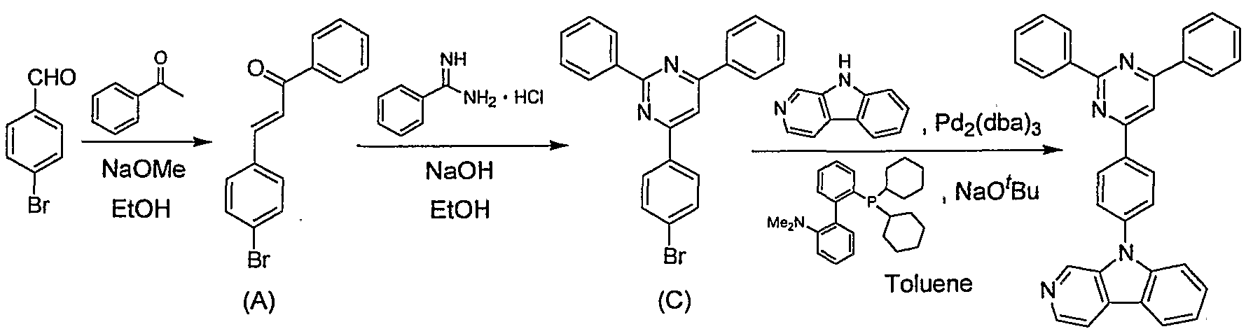
- Synthetic intermediate (A) 9. Og (31mraol), 1-Panacilpyridinium bromide 8.7e (31 brain 1), 19.3 g (250 mmol) of ammonium acetate was suspended in 27 mU of acetic acid, and the mixture was heated under reflux for 12 hours. The reaction solution was cooled to room temperature, toluene and water were added thereto, and after separating into two layers, the organic layer was washed successively with a 10% aqueous sodium hydroxide solution and a saturated saline solution, and dried over anhydrous sodium sulfate.
- Synthetic intermediate (B) 3.0 g (8 mmol), —carboline 1.4 g (8 mraol), tris (dibenzylideneacetone) dipalladium 0.18 g (0.2 imol), 2-dicyclohexylphosphino-1,2, I (N, N-dimethylamino) biphenyl 0.23 g (0.6 reference ol), sodium tert-butoxide 1.
- Og (l mmol) is suspended in 15 ml of toluene, and heated under an argon atmosphere for 20 hours under reflux. did. The reaction solution was cooled to room temperature, and methylene chloride and water were added.
- the obtained crystal was confirmed to be the target compound by 90 MHz ' ⁇ -NMR and FD-MS (field desorption mass spectrum).
- the FD-MS measurement results are shown below.
- Synthetic intermediate (A) 10. Og (35 mmol) and benzamidine hydrochloride 5.5 g (35 mmol) were suspended in 75 ml of ethanol, 2.8 g (70 mraol) of sodium hydroxide was added, and the mixture was heated under reflux for 18 hours. The reaction solution was cooled to room temperature, 50 ml of water was added, and the mixture was stirred for i hours. The precipitated crystal was filtered and washed with ethanol to obtain 8.2 g of a synthetic intermediate (C) (yield: 61%). (2) Synthesis of compound (2)
- Synthetic intermediate (D) 8. Dissolve lg (25 mmol) in 50 ral toluene and 50 ml of ether, add 21 ml of normal butyllithium hexane solution (1.6 M) (32 Mol) at -40 ° C under argon atmosphere, and add -40 The mixture was stirred at 0 ° C to 0 ° C for 1 hour. Next, the reaction solution was cooled to -70 ° C, a solution obtained by diluting 17 ml (74%) of triisopropyl borate in 25 ml of ether was added dropwise, and the mixture was stirred at -70 ° C for 1 hour, and then cooled to room temperature. The mixture was heated and stirred for 6 hours.
- the obtained crystals were confirmed to be the target compound by 90 MHz-NMR and FD-MS.
- the measurement results of FD-MS are shown below.
- Synthetic intermediate (F) 10.0 g (40 mraol), 0.90 g (4.0 mmol) of palladium acetate, and 5.9 g (56 iranol) of sodium carbonate were suspended in 80 ml of N, N-dimethylformamide, and the suspension was stirred under an argon atmosphere. Reflux with heating for hours. Cool the reaction solution to room temperature, add ethyl acetate and water. Then, after separating into two layers, the mixture was washed with water and saturated saline in this order, and dried with anhydrous sodium sulfate. After evaporating the organic solvent under reduced pressure, the crystals recrystallized from toluene were separated by filtration and washed with toluene to obtain 4.4 g of a synthetic intermediate (G) (yield 66%).
- the obtained crystal was confirmed to be the target compound by 90 MHz ' ⁇ -NMR and FD-MS.
- the results of FD-MS measurement are shown below.
- Compound (72) was prepared in the same manner as in (3) of Synthesis Example 1 except that synthetic intermediate (I) was used instead of synthetic intermediate (B) to obtain 1.8 g of crystals (yield). Rate 46%).
- the obtained crystals were confirmed to be the target compound by 90 MHz 'H-NMR and FD-MS.
- the results of FD-MS measurement are shown below.
- Synthesis intermediate (J) synthesized in the same manner as in Synthesis Examples (1) and (2) except that 3,5-dibromobenzaldehyde was used in place of 4-bromobenzaldehyde in (1) of Synthesis Example 1 above.
- 2.5 g (5 mmol) 2.5 g (5 mmol), ⁇ -carboline 1.0 g (6 mmol), tris (dibenzylideneacetone) dipalladium 0.18 g (0.2 country ol), 2-dicyclohexyl phosphinol 2,-(N, N-dimethylamino) biphenyl 0.23 g (0.6imnol), sodium tert-butoxide LOg (llmmol) in 15 ml of toluene Under an atmosphere, the mixture was heated under reflux for 20 hours.
- the reaction solution was cooled to room temperature, methylene chloride and water were added, and the mixture was separated into two layers, washed with water and dried over anhydrous sodium sulfate. After the organic solvent was distilled off under reduced pressure, the distillation residue was suspended in 15 ml of toluene, and 0.18 g (0.2 mmol) of tris (dibenzylidene aceton) dipalladium, 2-dicyclohexylphosphino 2 ′-(N, N —Dimethylamino) biphenyl (0.23 g, 0.6 mmol) and sodium tert-butoxide (1.0 g, ll-ol) were added, and the mixture was heated to reflux under an argon atmosphere for 20 hours.
- the reaction solution was cooled to room temperature, methylene chloride and water were added, and the mixture was separated into two layers, washed with water, and dried over anhydrous sodium sulfate. After evaporating the organic solvent under reduced pressure, the residue was purified by silica gel column chromatography to obtain crystal L7g (yield 53%).
- the obtained crystals were confirmed to be the target compound by 90 MHz 'H-NMR and FD-MS.
- the results of FD-MS measurement are shown below.
- Example 1 (manufacture of organic EL device)
- a 25 mm ⁇ 75 mm ⁇ 0.7 mm thick glass substrate with an ITO transparent electrode (manufactured by Geomatic) was subjected to ultrasonic cleaning in isopropyl alcohol for 5 minutes, and then UV ozone cleaning for 30 minutes.
- the glass substrate with the transparent electrode after cleaning is mounted on a substrate holder of a vacuum evaporation apparatus.
- the following copper having a film thickness of 10 nm is coated on the surface where the transparent electrode is formed so as to cover the transparent electrode.
- a phthalocyanine film hereinafter abbreviated as “CuPc film” was formed. This CuPc film functions as a hole injection layer.
- a-NPD film 4,4'-bis [N- (1-naphthyl) -N-phenylamino] biphenyl film (hereinafter abbreviated as “a-NPD film”) having a thickness of 3 Onm is formed on this CuPc film. did.
- This ⁇ -NPD film functions as a hole transport layer.
- the compound (1) having a thickness of 30 nm was deposited as a host material on the ⁇ -NPD film to form a light emitting layer.
- the following tris (2-phenylpyridine) Ir hereinafter abbreviated as “I r (ppy) 3 ”) was added as a phosphorescent Ir metal complex dopant.
- the concentration of I r (ppy) 3 in the light emitting layer was 5 wt 0/0.
- This membrane Functions as a light emitting layer.
- the following (1, ⁇ ⁇ -bisphenyl) -14-olato) bis (2-methyl-8-quino.linoleate) aluminum (hereinafter abbreviated as “BA1q film”) with a thickness of 10 nm ) was deposited.
- BA1q film functions as a hole barrier layer.
- This A 1 Q film functions as an electron injection layer.
- LiF which is an alkali metal halide
- aluminum was deposited to a thickness of 150 nm.
- This A 1 / L i F acts as a cathode.
- Table 1 shows the results obtained by measuring the triplet energy and singlet energy of the host material used in the light emitting layer by the above-mentioned measuring methods (1) and (2).
- This device was subjected to a conduction test to find that the voltage was 5.2 V and the current density was 0.
- Example 1 An organic EL device was prepared in the same manner as in Example 1 except that the compounds shown in Table 1 were used instead of the compound (1). Similarly, triplet energy and singlet energy, voltage, and current density were similarly measured. Table 1 shows the results of measuring the luminance, luminous efficiency, and chromaticity. Comparative Example 1
- An organic EL device was prepared in the same manner as in Example 1 except that the following compound '(BCz) was used instead of the compound (1), and a triplet energy, a singlet energy, a voltage Table 1 shows the results of measuring the current density, luminance, luminous efficiency, and chromaticity.
- Example 1 was repeated in the same manner as in Example 1 except that the following compound (A-10) described in U.S. Patent Publication No. 2002-283329 was used in place of compound (1).
- An EL device was manufactured, and the characteristics were evaluated in the same manner as in Example 1. Table 1 shows the results.
- Emission color Material (eV) (eV) (V) (mA / cm 2 ) (cd / m 2 ) (cd / A) (x, y)
- Example 1 (1) 2.8 3.4 5.2 0.26 99 38.6 (0.32,0.62) Green Example 2 (61) 2.6 3.3 5.5 0.24 102 42.8 (0.32,0.61) Green Example 3 (68) 2.7 3.5 5.6 0.27 100 37.2 (0.32 , 0.61) Green Comparative Example 1 (BCz) 2.8 3.6 5.4 0.31 101 32.6 (0.32,0.61) Green Comparative Example 2 (A-10) 3.1 3.7 5.9 0.32 100 31.8 (0.32,0.61) Green As shown in Table 1, Compared with the conventionally known compounds (BCz, A-10) of Comparative Examples 1 and 1, the organic EL device using the material for an organic EL device of the present invention can provide highly efficient green light emission. Further, since the material for an organic EL device of the present invention has a wide energy gap, light-emitting molecules having a wide energy gap can be mixed into a light-emitting layer to emit light.
- a 5 mm ⁇ 75 mm ⁇ 0.7 mm thick glass substrate with an ITO transparent electrode (manufactured by Geomatic Co., Ltd.) was subjected to ultrasonic cleaning in isopropyl alcohol for 5 minutes and then UV ozone cleaning for 30 minutes.
- the washed glass substrate with a transparent electrode is mounted on a substrate holder of a vacuum evaporation apparatus.
- the transparent electrode is formed on the surface on the side where the transparent electrode is formed so as to cover the transparent electrode.
- This CuPc film functions as a hole injection layer.
- the following 3 nm thick film is formed on the CuPc film.
- TPAC film A 1,1,1-bis [4-N, N-di (paratolyl) aminophenyl] cyclohexane film (hereinafter abbreviated as “TPAC film”) was formed.
- This TPAC membrane functions as a hole transport layer.
- the compound (1) having a thickness of 3 O nm was deposited on the TPAC film to form a light emitting layer.
- FI rpic (4,6-difluorophenyl) -pyridinato N, C 2 '] picolinate
- Table 1 shows the results obtained by measuring the triplet energy and singlet energy of the host material used in the light emitting layer by the above-mentioned measuring methods (1) and (2).
- An organic EL device was prepared in the same manner as in Example 4 except that the compound shown in Table 2 was used instead of the compound (1), and the triplet energy and singlet energy, voltage, and current were similarly measured.
- Table 2 shows the measurement results of density, luminance, luminous efficiency, and chromaticity. Comparative Example 3
- An organic EL device was prepared in the same manner as in Example 4 except that the above compound (BCz) was used instead of the compound (1), and a triplet energy and a singlet energy were similarly produced.
- Table 2 shows the measurement results of voltage, current density, luminance, luminous efficiency, and chromaticity. Comparative Example 4
- Comparative Example 3 the compound ( ⁇ -NPD) was used in place of the compound (TPAC) in the hole transport layer, and the compound (BA1) was used in place of the compound (Alq) in the electron injection layer.
- An organic EL device was fabricated in the same manner except that q) was used, and the triplet energy and singlet energy, voltage, current density, luminance, luminous efficiency, and chromaticity were measured in the same manner as shown in Table 2. Was.
- the organic EL device using the material for an organic EL device of the present invention was driven at a lower voltage and higher in efficiency than the conventionally known compound (BCz) of Comparative Examples 3 and 4. Blue light emission is obtained. Further, since the material for an organic EL device of the present invention has a wide energy gap, light-emitting molecules having a wide energy gap can be mixed into the light-emitting layer to emit light. Industrial applicability
- the use of a material for an organic EL device comprising the compound represented by the general formula (1) of the present invention makes it possible to utilize luminescent light, achieve low voltage, and achieve luminous efficiency.
- a high organic electroluminescent device can be obtained. Therefore, the organic electroluminescent device of the present invention is extremely useful as a light source for various electronic devices.
Abstract
Description


Claims

Priority Applications (3)
| Application Number | Priority Date | Filing Date | Title |
|---|---|---|---|
| JP2004558476A JP4541152B2 (ja) | 2002-12-12 | 2003-12-11 | 有機エレクトロルミネッセンス素子用材料及びそれを用いた有機エレクトロルミネッセンス素子 |
| EP03778817A EP1571193A4 (en) | 2002-12-12 | 2003-12-11 | ORGANIC MATERIAL FOR ELECTROLUMINESCENZING DEVICE AND ORIGINAL ELECTROLUMINESCENZING DEVICE BASED ON IT |
| US10/538,023 US20060251918A1 (en) | 2003-12-11 | 2003-12-11 | Organic electroluminescent device material and organic electroluminescent device using same |
Applications Claiming Priority (2)
| Application Number | Priority Date | Filing Date | Title |
|---|---|---|---|
| JP2002360134 | 2002-12-12 | ||
| JP2002-360134 | 2002-12-12 |
Publications (1)
| Publication Number | Publication Date |
|---|---|
| WO2004053019A1 true WO2004053019A1 (ja) | 2004-06-24 |
Family
ID=32500975
Family Applications (1)
| Application Number | Title | Priority Date | Filing Date |
|---|---|---|---|
| PCT/JP2003/015874 WO2004053019A1 (ja) | 2002-12-12 | 2003-12-11 | 有機エレクトロルミネッセンス素子用材料及びそれを用いた有機エレクトロルミネッセンス素子 |
Country Status (6)
| Country | Link |
|---|---|
| EP (1) | EP1571193A4 (ja) |
| JP (1) | JP4541152B2 (ja) |
| KR (1) | KR101035780B1 (ja) |
| CN (1) | CN100338172C (ja) |
| TW (1) | TW200414821A (ja) |
| WO (1) | WO2004053019A1 (ja) |
Cited By (44)
| Publication number | Priority date | Publication date | Assignee | Title |
|---|---|---|---|---|
| JP2004281087A (ja) * | 2003-03-12 | 2004-10-07 | Nippon Hoso Kyokai <Nhk> | 有機elデバイスおよび有機elディスプレイ |
| WO2004095891A1 (ja) * | 2003-04-23 | 2004-11-04 | Konica Minolta Holdings, Inc. | 有機エレクトロルミネッセンス素子用材料、有機エレクトロルミネッセンス素子、照明装置、表示装置 |
| WO2005039246A1 (ja) * | 2003-09-30 | 2005-04-28 | Konica Minolta Holdings, Inc. | 有機エレクトロルミネッセンス素子、照明装置、表示装置 |
| JP2005340123A (ja) * | 2004-05-31 | 2005-12-08 | Konica Minolta Holdings Inc | 有機エレクトロルミネッセンス素子、照明装置及び表示装置 |
| JP2005347160A (ja) * | 2004-06-04 | 2005-12-15 | Konica Minolta Holdings Inc | 有機エレクトロルミネッセンス素子、照明装置及び表示装置 |
| JP2006032599A (ja) * | 2004-07-15 | 2006-02-02 | Konica Minolta Holdings Inc | 有機エレクトロルミネッセンス素子、照明装置及び表示装置 |
| WO2006013739A1 (ja) * | 2004-08-04 | 2006-02-09 | Konica Minolta Holdings, Inc. | 有機エレクトロルミネッセンス素子、照明装置及び表示装置 |
| JP2006060198A (ja) * | 2004-07-23 | 2006-03-02 | Konica Minolta Holdings Inc | 有機エレクトロルミネッセンス素子、表示装置及び照明装置 |
| JP2006066580A (ja) * | 2004-08-26 | 2006-03-09 | Konica Minolta Holdings Inc | 有機エレクトロルミネッセンス素子用材料、有機エレクトロルミネッセンス素子、照明装置および表示装置 |
| WO2006043440A1 (ja) * | 2004-10-19 | 2006-04-27 | Konica Minolta Holdings, Inc. | 有機エレクトロルミネッセンス素子、表示装置及び照明装置 |
| JP2006120906A (ja) * | 2004-10-22 | 2006-05-11 | Konica Minolta Holdings Inc | 有機エレクトロルミネッセンス素子、表示装置及び照明装置 |
| JP2006120763A (ja) * | 2004-10-20 | 2006-05-11 | Konica Minolta Holdings Inc | 有機エレクトロルミネッセンス素子、照明装置及び表示装置 |
| JP2006120821A (ja) * | 2004-10-21 | 2006-05-11 | Konica Minolta Holdings Inc | 有機エレクトロルミネッセンス素子、照明装置および表示装置 |
| JP2006120762A (ja) * | 2004-10-20 | 2006-05-11 | Konica Minolta Holdings Inc | 有機エレクトロルミネッセンス素子、表示装置及び照明装置 |
| JP2006120689A (ja) * | 2004-10-19 | 2006-05-11 | Konica Minolta Holdings Inc | 有機エレクトロルミネッセンス素子、表示装置及び照明装置 |
| JP2006128257A (ja) * | 2004-10-27 | 2006-05-18 | Konica Minolta Holdings Inc | 有機el素子、その製造方法及び該有機el素子を用いた照明又は表示素子 |
| WO2006070619A1 (ja) * | 2004-12-28 | 2006-07-06 | Konica Minolta Holdings, Inc. | 有機エレクトロルミネッセンス素子、表示装置及び照明装置 |
| WO2006100888A1 (ja) * | 2005-03-22 | 2006-09-28 | Konica Minolta Holdings, Inc. | 有機el素子用材料、有機el素子、表示装置及び照明装置 |
| WO2006126389A1 (ja) * | 2005-05-25 | 2006-11-30 | Konica Minolta Holdings, Inc. | 有機エレクトロルミネッセンス素子材料、有機エレクトロルミネッセンス素子、表示装置及び照明装置 |
| WO2007004380A1 (ja) * | 2005-07-01 | 2007-01-11 | Konica Minolta Holdings, Inc. | 有機エレクトロルミネッセンス素子材料、有機エレクトロルミネッセンス素子、表示装置及び照明装置 |
| WO2007023659A1 (ja) * | 2005-08-25 | 2007-03-01 | Konica Minolta Holdings, Inc. | 有機エレクトロルミネッセンス素子材料、有機エレクトロルミネッセンス素子、表示装置及び照明装置 |
| JPWO2006008976A1 (ja) * | 2004-07-16 | 2008-05-01 | コニカミノルタホールディングス株式会社 | 白色発光有機エレクトロルミネッセンス素子、表示装置及び照明装置 |
| WO2008114690A1 (ja) * | 2007-03-15 | 2008-09-25 | Hodogaya Chemical Co., Ltd. | 置換されたビピリジル基とピリドインドール環構造がフェニレン基を介して連結した化合物および有機エレクトロルミネッセンス素子 |
| US20080303415A1 (en) * | 2004-08-05 | 2008-12-11 | Yoshiyuki Suzuri | Organic Electroluminescence Element, Display and Illuminator |
| WO2009096549A1 (ja) * | 2008-01-31 | 2009-08-06 | Hodogaya Chemical Co., Ltd. | 置換されたピリジル基とピリドインドール環構造がフェニレン基を介して連結した化合物および有機エレクトロルミネッセンス素子 |
| WO2009102016A1 (ja) * | 2008-02-14 | 2009-08-20 | Hodogaya Chemical Co., Ltd. | 置換されたピリジル基が連結したピリドインドール環構造を有する化合物および有機エレクトロルミネッセンス素子 |
| WO2009139475A1 (ja) * | 2008-05-16 | 2009-11-19 | 保土谷化学工業株式会社 | 有機エレクトロルミネッセンス素子 |
| JP2010031248A (ja) * | 2008-06-23 | 2010-02-12 | Sumitomo Chemical Co Ltd | 組成物及び該組成物を用いてなる発光素子 |
| JPWO2008056746A1 (ja) * | 2006-11-09 | 2010-02-25 | 新日鐵化学株式会社 | 有機電界発光素子用化合物及び有機電界発光素子 |
| WO2010035723A1 (ja) * | 2008-09-24 | 2010-04-01 | 保土谷化学工業株式会社 | 置換されたアントラセン環構造とピリドインドール環構造を有する化合物および有機エレクトロルミネッセンス素子 |
| WO2011016202A1 (ja) * | 2009-08-05 | 2011-02-10 | 保土谷化学工業株式会社 | 置換されたアントラセン環構造とピリドインドール環構造を有する化合物および有機エレクトロルミネッセンス素子 |
| US7902196B2 (en) | 2005-03-17 | 2011-03-08 | President And Fellows Of Harvard College | Synthesis of avrainvillamide, strephacidin B, and analogues thereof |
| JP2011093825A (ja) * | 2009-10-28 | 2011-05-12 | Hodogaya Chem Co Ltd | 2,2−ジフェニルアダマンチル構造を有する化合物および有機エレクトロルミネッセンス素子 |
| JP2011146726A (ja) * | 2011-02-22 | 2011-07-28 | Konica Minolta Holdings Inc | 有機エレクトロルミネッセンス素子、照明装置及び表示装置 |
| JP2011228723A (ja) * | 2004-07-23 | 2011-11-10 | Konica Minolta Holdings Inc | 有機エレクトロルミネッセンス素子、表示装置及び照明装置 |
| JP2012138585A (ja) * | 2005-04-18 | 2012-07-19 | Konica Minolta Holdings Inc | 有機エレクトロルミネッセンス素子、表示装置及び照明装置 |
| WO2012098849A1 (ja) * | 2011-01-18 | 2012-07-26 | 保土谷化学工業株式会社 | 置換されたビピリジル基とピリドインドール環構造を有する化合物および有機エレクトロルミネッセンス素子 |
| JP2012256910A (ja) * | 2006-02-20 | 2012-12-27 | Konica Minolta Holdings Inc | 有機エレクトロルミネッセンス素子、白色発光素子、表示装置、及び照明装置 |
| WO2014007287A1 (ja) | 2012-07-05 | 2014-01-09 | 東レ株式会社 | 発光素子材料および発光素子 |
| JP2014027289A (ja) * | 2013-09-02 | 2014-02-06 | Konica Minolta Inc | 有機エレクトロルミネッセンス素子 |
| JP2015010092A (ja) * | 2013-06-28 | 2015-01-19 | ユニバーサル ディスプレイ コーポレイション | Pholed用の新規ホスト材料 |
| US9318711B2 (en) | 2012-11-20 | 2016-04-19 | Samsung Display Co., Ltd. | Organic electroluminescence materials comprising substituted carbazoles and organic electroluminescence devices having the same |
| WO2018181370A1 (ja) * | 2017-03-28 | 2018-10-04 | 保土谷化学工業株式会社 | アザカルバゾール構造を有する化合物および有機エレクトロルミネッセンス素子 |
| CN112724136A (zh) * | 2020-12-28 | 2021-04-30 | 上海天马有机发光显示技术有限公司 | 一种有机化合物、电致发光材料及其应用 |
Families Citing this family (19)
| Publication number | Priority date | Publication date | Assignee | Title |
|---|---|---|---|---|
| US20060180806A1 (en) * | 2003-01-24 | 2006-08-17 | Takashi Arakane | Organic electroluminescence device |
| CN100492709C (zh) * | 2003-04-23 | 2009-05-27 | 柯尼卡美能达控股株式会社 | 有机电致发光元件和显示装置 |
| US20090091253A1 (en) | 2006-03-17 | 2009-04-09 | Konica Minolta Holdings, Inc. | Organic electroluminescent element, display device and lighting device |
| EP2557138B1 (en) | 2006-03-23 | 2016-08-10 | Konica Minolta Holdings, Inc. | Organic electroluminescent device, display and illuminating device |
| US20080090834A1 (en) * | 2006-07-06 | 2008-04-17 | Pfizer Inc | Selective azole pde10a inhibitor compounds |
| US8168308B2 (en) | 2006-08-18 | 2012-05-01 | Hodogaya Chemical Co., Ltd. | Compound having pyridoindole ring structure having substituted pyridyl group attached thereto, and organic electroluminescence element |
| JP6016207B2 (ja) | 2008-10-02 | 2016-10-26 | ユー・ディー・シー アイルランド リミテッド | 錯塩 |
| KR101233375B1 (ko) * | 2008-12-24 | 2013-02-15 | 제일모직주식회사 | 신규한 유기광전소자용 화합물 및 이를 포함하는 유기광전소자 |
| KR101288557B1 (ko) | 2008-12-24 | 2013-07-22 | 제일모직주식회사 | 신규한 유기광전소자용 화합물 및 이를 포함하는 유기광전소자 |
| KR101872407B1 (ko) | 2011-06-22 | 2018-08-01 | 삼성디스플레이 주식회사 | 헤테로고리 화합물, 이를 포함하는 유기 발광 소자 및 평판 표시 장치 |
| KR102192001B1 (ko) * | 2014-03-31 | 2020-12-16 | 엘지디스플레이 주식회사 | 카바졸 화합물 및 이를 포함하는 유기발광소자 |
| KR101706659B1 (ko) * | 2014-05-22 | 2017-02-17 | (주)아이티켐 | 신규한 유기발광화합물 및 이를 이용한 유기발광소자 |
| CN105085551B (zh) * | 2015-06-04 | 2017-09-22 | 北京拓彩光电科技有限公司 | 芳香杂环衍生物和使用该化合物的有机发光二极管器件 |
| KR101965928B1 (ko) * | 2015-06-29 | 2019-04-04 | 주식회사 두산 | 유기 발광 화합물 및 이를 이용한 유기 전계 발광 소자 |
| CN105118918B (zh) * | 2015-07-21 | 2017-06-20 | 苏州大学 | 一种有机‑无机杂化电荷注入层的制备方法 |
| CN105384759B (zh) * | 2015-10-22 | 2017-12-15 | 北京拓彩光电科技有限公司 | 芳香杂环衍生物和使用该化合物的有机发光二极管器件 |
| KR102587382B1 (ko) * | 2016-04-29 | 2023-10-12 | 솔루스첨단소재 주식회사 | 유기 발광 화합물 및 이를 이용한 유기 전계 발광 소자 |
| CN109309163B (zh) * | 2017-07-26 | 2019-12-17 | 清华大学 | 一种有机电致发光器件 |
| EP3858831A4 (en) * | 2018-09-28 | 2022-04-20 | LT Materials Co., Ltd. | HETEROCYCLIC COMPOUND AND ORGANIC LIGHT EMITTING DIOD WITH IT |
Citations (5)
| Publication number | Priority date | Publication date | Assignee | Title |
|---|---|---|---|---|
| JPS5411736A (en) * | 1977-06-28 | 1979-01-29 | Ricoh Co Ltd | Photoreceptor for electrophotography |
| JPS63293550A (ja) * | 1987-05-27 | 1988-11-30 | Canon Inc | 電子写真感光体 |
| JPH02108058A (ja) * | 1988-10-18 | 1990-04-19 | Canon Inc | 電子写真感光体 |
| JP2001160488A (ja) * | 1999-12-01 | 2001-06-12 | Konica Corp | 有機エレクトロルミネッセンス素子 |
| EP1246510A1 (en) * | 2000-11-27 | 2002-10-02 | Idemitsu Kosan Co., Ltd. | Organic electroluminescence device |
Family Cites Families (6)
| Publication number | Priority date | Publication date | Assignee | Title |
|---|---|---|---|---|
| US3415831A (en) * | 1965-07-16 | 1968-12-10 | Smith Kline French Lab | 2-isoquinolinyl(and carbolinyl) alkyloctahydroindolo [2,3-a]-quinolizines |
| JPS5291893A (en) * | 1976-01-23 | 1977-08-02 | Sumitomo Chem Co Ltd | Preparation of indroquinoline derivatives |
| JPH07110940B2 (ja) * | 1991-06-05 | 1995-11-29 | 住友化学工業株式会社 | 有機エレクトロルミネッセンス素子 |
| DE19502753A1 (de) * | 1995-01-23 | 1996-07-25 | Schering Ag | Neue 9H-Pyrido[3,4-b]indol-Derivate |
| TW532048B (en) * | 2000-03-27 | 2003-05-11 | Idemitsu Kosan Co | Organic electroluminescence element |
| JP4061840B2 (ja) * | 2000-12-28 | 2008-03-19 | 凸版印刷株式会社 | 有機薄膜発光素子用の正孔輸送性化合物および有機薄膜発光素子 |
-
2003
- 2003-12-11 CN CNB2003801057064A patent/CN100338172C/zh not_active Expired - Fee Related
- 2003-12-11 TW TW092135060A patent/TW200414821A/zh not_active IP Right Cessation
- 2003-12-11 KR KR1020057010613A patent/KR101035780B1/ko active IP Right Grant
- 2003-12-11 JP JP2004558476A patent/JP4541152B2/ja not_active Expired - Fee Related
- 2003-12-11 EP EP03778817A patent/EP1571193A4/en not_active Withdrawn
- 2003-12-11 WO PCT/JP2003/015874 patent/WO2004053019A1/ja active Application Filing
Patent Citations (5)
| Publication number | Priority date | Publication date | Assignee | Title |
|---|---|---|---|---|
| JPS5411736A (en) * | 1977-06-28 | 1979-01-29 | Ricoh Co Ltd | Photoreceptor for electrophotography |
| JPS63293550A (ja) * | 1987-05-27 | 1988-11-30 | Canon Inc | 電子写真感光体 |
| JPH02108058A (ja) * | 1988-10-18 | 1990-04-19 | Canon Inc | 電子写真感光体 |
| JP2001160488A (ja) * | 1999-12-01 | 2001-06-12 | Konica Corp | 有機エレクトロルミネッセンス素子 |
| EP1246510A1 (en) * | 2000-11-27 | 2002-10-02 | Idemitsu Kosan Co., Ltd. | Organic electroluminescence device |
Non-Patent Citations (1)
| Title |
|---|
| See also references of EP1571193A4 * |
Cited By (81)
| Publication number | Priority date | Publication date | Assignee | Title |
|---|---|---|---|---|
| JP2004281087A (ja) * | 2003-03-12 | 2004-10-07 | Nippon Hoso Kyokai <Nhk> | 有機elデバイスおよび有機elディスプレイ |
| US7749619B2 (en) | 2003-04-23 | 2010-07-06 | Konica Minolta Holdings, Inc. | Organic electroluminescent element and display |
| WO2004095891A1 (ja) * | 2003-04-23 | 2004-11-04 | Konica Minolta Holdings, Inc. | 有機エレクトロルミネッセンス素子用材料、有機エレクトロルミネッセンス素子、照明装置、表示装置 |
| WO2004095889A1 (ja) * | 2003-04-23 | 2004-11-04 | Konica Minolta Holdings, Inc. | 有機エレクトロルミネッセンス素子及び表示装置 |
| WO2004095890A1 (ja) * | 2003-04-23 | 2004-11-04 | Konica Minolta Holdings, Inc. | 有機エレクトロルミネッセンス素子用材料、有機エレクトロルミネッセンス素子、照明装置、表示装置 |
| JPWO2004095890A1 (ja) * | 2003-04-23 | 2006-07-13 | コニカミノルタホールディングス株式会社 | 有機エレクトロルミネッセンス素子用材料、有機エレクトロルミネッセンス素子、照明装置、表示装置 |
| US7326475B2 (en) | 2003-04-23 | 2008-02-05 | Konica Minolta Holdings, Inc. | Material for organic electroluminescent device, organic electroluminescent device, illuminating device and display |
| JP4635869B2 (ja) * | 2003-04-23 | 2011-02-23 | コニカミノルタホールディングス株式会社 | 有機エレクトロルミネッセンス素子、照明装置、表示装置 |
| US7740955B2 (en) | 2003-04-23 | 2010-06-22 | Konica Minolta Holdings, Inc. | Organic electroluminescent device and display |
| WO2005039246A1 (ja) * | 2003-09-30 | 2005-04-28 | Konica Minolta Holdings, Inc. | 有機エレクトロルミネッセンス素子、照明装置、表示装置 |
| JP2005340123A (ja) * | 2004-05-31 | 2005-12-08 | Konica Minolta Holdings Inc | 有機エレクトロルミネッセンス素子、照明装置及び表示装置 |
| JP2005347160A (ja) * | 2004-06-04 | 2005-12-15 | Konica Minolta Holdings Inc | 有機エレクトロルミネッセンス素子、照明装置及び表示装置 |
| JP2006032599A (ja) * | 2004-07-15 | 2006-02-02 | Konica Minolta Holdings Inc | 有機エレクトロルミネッセンス素子、照明装置及び表示装置 |
| JPWO2006008976A1 (ja) * | 2004-07-16 | 2008-05-01 | コニカミノルタホールディングス株式会社 | 白色発光有機エレクトロルミネッセンス素子、表示装置及び照明装置 |
| US8329317B2 (en) | 2004-07-16 | 2012-12-11 | Konica Minolta Holdings, Inc. | White light emitting organic electroluminescence element, display and illuminator |
| JP2006060198A (ja) * | 2004-07-23 | 2006-03-02 | Konica Minolta Holdings Inc | 有機エレクトロルミネッセンス素子、表示装置及び照明装置 |
| JP2011228723A (ja) * | 2004-07-23 | 2011-11-10 | Konica Minolta Holdings Inc | 有機エレクトロルミネッセンス素子、表示装置及び照明装置 |
| WO2006013739A1 (ja) * | 2004-08-04 | 2006-02-09 | Konica Minolta Holdings, Inc. | 有機エレクトロルミネッセンス素子、照明装置及び表示装置 |
| JPWO2006013739A1 (ja) * | 2004-08-04 | 2008-05-01 | コニカミノルタホールディングス株式会社 | 有機エレクトロルミネッセンス素子、照明装置及び表示装置 |
| JP4626613B2 (ja) * | 2004-08-04 | 2011-02-09 | コニカミノルタホールディングス株式会社 | 有機エレクトロルミネッセンス素子 |
| US20080303415A1 (en) * | 2004-08-05 | 2008-12-11 | Yoshiyuki Suzuri | Organic Electroluminescence Element, Display and Illuminator |
| JP2006066580A (ja) * | 2004-08-26 | 2006-03-09 | Konica Minolta Holdings Inc | 有機エレクトロルミネッセンス素子用材料、有機エレクトロルミネッセンス素子、照明装置および表示装置 |
| WO2006043440A1 (ja) * | 2004-10-19 | 2006-04-27 | Konica Minolta Holdings, Inc. | 有機エレクトロルミネッセンス素子、表示装置及び照明装置 |
| JP5309446B2 (ja) * | 2004-10-19 | 2013-10-09 | コニカミノルタ株式会社 | 有機エレクトロルミネッセンス素子、表示装置及び照明装置 |
| JP2006120689A (ja) * | 2004-10-19 | 2006-05-11 | Konica Minolta Holdings Inc | 有機エレクトロルミネッセンス素子、表示装置及び照明装置 |
| JPWO2006043440A1 (ja) * | 2004-10-19 | 2008-05-22 | コニカミノルタホールディングス株式会社 | 有機エレクトロルミネッセンス素子、表示装置及び照明装置 |
| JP2006120762A (ja) * | 2004-10-20 | 2006-05-11 | Konica Minolta Holdings Inc | 有機エレクトロルミネッセンス素子、表示装置及び照明装置 |
| JP2006120763A (ja) * | 2004-10-20 | 2006-05-11 | Konica Minolta Holdings Inc | 有機エレクトロルミネッセンス素子、照明装置及び表示装置 |
| JP2006120821A (ja) * | 2004-10-21 | 2006-05-11 | Konica Minolta Holdings Inc | 有機エレクトロルミネッセンス素子、照明装置および表示装置 |
| JP2006120906A (ja) * | 2004-10-22 | 2006-05-11 | Konica Minolta Holdings Inc | 有機エレクトロルミネッセンス素子、表示装置及び照明装置 |
| JP2006128257A (ja) * | 2004-10-27 | 2006-05-18 | Konica Minolta Holdings Inc | 有機el素子、その製造方法及び該有機el素子を用いた照明又は表示素子 |
| WO2006070619A1 (ja) * | 2004-12-28 | 2006-07-06 | Konica Minolta Holdings, Inc. | 有機エレクトロルミネッセンス素子、表示装置及び照明装置 |
| JPWO2006070619A1 (ja) * | 2004-12-28 | 2008-06-12 | コニカミノルタホールディングス株式会社 | 有機エレクトロルミネッセンス素子、表示装置及び照明装置 |
| JP5056016B2 (ja) * | 2004-12-28 | 2012-10-24 | コニカミノルタホールディングス株式会社 | 有機エレクトロルミネッセンス素子、表示装置及び照明装置 |
| US7902196B2 (en) | 2005-03-17 | 2011-03-08 | President And Fellows Of Harvard College | Synthesis of avrainvillamide, strephacidin B, and analogues thereof |
| WO2006100888A1 (ja) * | 2005-03-22 | 2006-09-28 | Konica Minolta Holdings, Inc. | 有機el素子用材料、有機el素子、表示装置及び照明装置 |
| JP2012138585A (ja) * | 2005-04-18 | 2012-07-19 | Konica Minolta Holdings Inc | 有機エレクトロルミネッセンス素子、表示装置及び照明装置 |
| WO2006126389A1 (ja) * | 2005-05-25 | 2006-11-30 | Konica Minolta Holdings, Inc. | 有機エレクトロルミネッセンス素子材料、有機エレクトロルミネッセンス素子、表示装置及び照明装置 |
| US9099659B2 (en) | 2005-07-01 | 2015-08-04 | Konica Minolta, Inc. | Organic electroluminescent element material, organic electroluminescent element, display device, and lighting device |
| WO2007004380A1 (ja) * | 2005-07-01 | 2007-01-11 | Konica Minolta Holdings, Inc. | 有機エレクトロルミネッセンス素子材料、有機エレクトロルミネッセンス素子、表示装置及び照明装置 |
| JP5076891B2 (ja) * | 2005-07-01 | 2012-11-21 | コニカミノルタホールディングス株式会社 | 有機エレクトロルミネッセンス素子材料、有機エレクトロルミネッセンス素子、表示装置及び照明装置 |
| US9379337B2 (en) | 2005-07-01 | 2016-06-28 | Konica Minolta, Inc. | Organic electroluminescent element material, organic electroluminescent element, display device, and lighting device |
| WO2007023659A1 (ja) * | 2005-08-25 | 2007-03-01 | Konica Minolta Holdings, Inc. | 有機エレクトロルミネッセンス素子材料、有機エレクトロルミネッセンス素子、表示装置及び照明装置 |
| JP2012256910A (ja) * | 2006-02-20 | 2012-12-27 | Konica Minolta Holdings Inc | 有機エレクトロルミネッセンス素子、白色発光素子、表示装置、及び照明装置 |
| JPWO2008056746A1 (ja) * | 2006-11-09 | 2010-02-25 | 新日鐵化学株式会社 | 有機電界発光素子用化合物及び有機電界発光素子 |
| WO2008114690A1 (ja) * | 2007-03-15 | 2008-09-25 | Hodogaya Chemical Co., Ltd. | 置換されたビピリジル基とピリドインドール環構造がフェニレン基を介して連結した化合物および有機エレクトロルミネッセンス素子 |
| JP5352447B2 (ja) * | 2007-03-15 | 2013-11-27 | 保土谷化学工業株式会社 | 置換されたビピリジル基とピリドインドール環構造がフェニレン基を介して連結した化合物および有機エレクトロルミネッセンス素子 |
| KR101487567B1 (ko) | 2007-03-15 | 2015-01-29 | 호도가야 가가쿠 고교 가부시키가이샤 | 치환된 비피리딜기와 피리도인돌환 구조가 페닐렌기를 통해 연결된 화합물 및 유기 전계발광 소자 |
| US8252431B2 (en) | 2007-03-15 | 2012-08-28 | Hodogaya Chemical Co., Ltd. | Compound wherein substituted bipyridyl group is connected with pyridoindole ring structure through phenylene group, and organic electroluminescent device |
| JPWO2009096549A1 (ja) * | 2008-01-31 | 2011-05-26 | 保土谷化学工業株式会社 | 置換されたピリジル基とピリドインドール環構造がフェニレン基を介して連結した化合物および有機エレクトロルミネッセンス素子 |
| WO2009096549A1 (ja) * | 2008-01-31 | 2009-08-06 | Hodogaya Chemical Co., Ltd. | 置換されたピリジル基とピリドインドール環構造がフェニレン基を介して連結した化合物および有機エレクトロルミネッセンス素子 |
| US8377573B2 (en) | 2008-01-31 | 2013-02-19 | Hodogaya Chemical Co., Ltd. | Compound having substituted pyridyl group and pyridoindole ring structure linked through phenylene group, and organic electroluminescent device |
| JP2014114287A (ja) * | 2008-02-14 | 2014-06-26 | Hodogaya Chem Co Ltd | 置換されたピリジル基が連結したピリドインドール環構造を有する化合物および有機エレクトロルミネッセンス素子 |
| JP5467873B2 (ja) * | 2008-02-14 | 2014-04-09 | 保土谷化学工業株式会社 | 置換されたピリジル基が連結したピリドインドール環構造を有する化合物および有機エレクトロルミネッセンス素子 |
| WO2009102016A1 (ja) * | 2008-02-14 | 2009-08-20 | Hodogaya Chemical Co., Ltd. | 置換されたピリジル基が連結したピリドインドール環構造を有する化合物および有機エレクトロルミネッセンス素子 |
| JPWO2009102016A1 (ja) * | 2008-02-14 | 2011-06-16 | 保土谷化学工業株式会社 | 置換されたピリジル基が連結したピリドインドール環構造を有する化合物および有機エレクトロルミネッセンス素子 |
| US8624228B2 (en) | 2008-02-14 | 2014-01-07 | Hodogaya Chemical Co., Ltd. | Compound having pyridoindole ring structure bonded with substituted pyridyl group, and organic electroluminescent device |
| US9525140B2 (en) | 2008-05-16 | 2016-12-20 | Hodogaya Chemical Co., Ltd. | Arylamine compound useful in an organic electroluminescent device |
| US8771841B2 (en) | 2008-05-16 | 2014-07-08 | Hodogaya Chemical Co., Ltd. | Organic electroluminescent device |
| WO2009139475A1 (ja) * | 2008-05-16 | 2009-11-19 | 保土谷化学工業株式会社 | 有機エレクトロルミネッセンス素子 |
| JPWO2009139475A1 (ja) * | 2008-05-16 | 2011-09-22 | 保土谷化学工業株式会社 | 有機エレクトロルミネッセンス素子 |
| JP2010031248A (ja) * | 2008-06-23 | 2010-02-12 | Sumitomo Chemical Co Ltd | 組成物及び該組成物を用いてなる発光素子 |
| US8586210B2 (en) | 2008-09-24 | 2013-11-19 | Hodogaya Chemical Co., Ltd. | Compound having substituted anthracene ring structure and pyridoindole ring structure and organic electroluminescence device |
| WO2010035723A1 (ja) * | 2008-09-24 | 2010-04-01 | 保土谷化学工業株式会社 | 置換されたアントラセン環構造とピリドインドール環構造を有する化合物および有機エレクトロルミネッセンス素子 |
| JP5832746B2 (ja) * | 2008-09-24 | 2015-12-16 | 保土谷化学工業株式会社 | 置換されたアントラセン環構造とピリドインドール環構造を有する化合物および有機エレクトロルミネッセンス素子 |
| WO2011016202A1 (ja) * | 2009-08-05 | 2011-02-10 | 保土谷化学工業株式会社 | 置換されたアントラセン環構造とピリドインドール環構造を有する化合物および有機エレクトロルミネッセンス素子 |
| US9755152B2 (en) | 2009-08-05 | 2017-09-05 | Hodogaya Chemical Co., Ltd. | Compound having substituted anthracene ring structure and pyridoindole ring structure, and organic electroluminescent device |
| US8927119B2 (en) | 2009-08-05 | 2015-01-06 | Hodogaya Chemical Co., Ltd. | Compound having substituted anthracene ring structure and pyridoindole ring structure, and organic electroluminescent device |
| JP2011093825A (ja) * | 2009-10-28 | 2011-05-12 | Hodogaya Chem Co Ltd | 2,2−ジフェニルアダマンチル構造を有する化合物および有機エレクトロルミネッセンス素子 |
| US10541369B2 (en) | 2011-01-18 | 2020-01-21 | Hodogaya Chemical Co., Ltd. | Compound having substituted bipyridyl group and pyridoinodole ring structure, and organic electroluminescent device |
| WO2012098849A1 (ja) * | 2011-01-18 | 2012-07-26 | 保土谷化学工業株式会社 | 置換されたビピリジル基とピリドインドール環構造を有する化合物および有機エレクトロルミネッセンス素子 |
| JP5955228B2 (ja) * | 2011-01-18 | 2016-07-20 | 保土谷化学工業株式会社 | 置換されたビピリジル基とピリドインドール環構造を有する化合物および有機エレクトロルミネッセンス素子 |
| JP2011146726A (ja) * | 2011-02-22 | 2011-07-28 | Konica Minolta Holdings Inc | 有機エレクトロルミネッセンス素子、照明装置及び表示装置 |
| KR20150035706A (ko) | 2012-07-05 | 2015-04-07 | 도레이 카부시키가이샤 | 발광 소자 재료 및 발광 소자 |
| WO2014007287A1 (ja) | 2012-07-05 | 2014-01-09 | 東レ株式会社 | 発光素子材料および発光素子 |
| US9318711B2 (en) | 2012-11-20 | 2016-04-19 | Samsung Display Co., Ltd. | Organic electroluminescence materials comprising substituted carbazoles and organic electroluminescence devices having the same |
| JP2015010092A (ja) * | 2013-06-28 | 2015-01-19 | ユニバーサル ディスプレイ コーポレイション | Pholed用の新規ホスト材料 |
| JP2014027289A (ja) * | 2013-09-02 | 2014-02-06 | Konica Minolta Inc | 有機エレクトロルミネッセンス素子 |
| WO2018181370A1 (ja) * | 2017-03-28 | 2018-10-04 | 保土谷化学工業株式会社 | アザカルバゾール構造を有する化合物および有機エレクトロルミネッセンス素子 |
| CN112724136A (zh) * | 2020-12-28 | 2021-04-30 | 上海天马有机发光显示技术有限公司 | 一种有机化合物、电致发光材料及其应用 |
| CN112724136B (zh) * | 2020-12-28 | 2023-04-18 | 武汉天马微电子有限公司 | 一种有机化合物、电致发光材料及其应用 |
Also Published As
| Publication number | Publication date |
|---|---|
| JPWO2004053019A1 (ja) | 2006-04-13 |
| EP1571193A1 (en) | 2005-09-07 |
| TW200414821A (en) | 2004-08-01 |
| JP4541152B2 (ja) | 2010-09-08 |
| CN100338172C (zh) | 2007-09-19 |
| KR101035780B1 (ko) | 2011-05-20 |
| EP1571193A4 (en) | 2008-05-07 |
| KR20050085550A (ko) | 2005-08-29 |
| CN1723258A (zh) | 2006-01-18 |
| TWI359182B (ja) | 2012-03-01 |
Similar Documents
| Publication | Publication Date | Title |
|---|---|---|
| WO2004053019A1 (ja) | 有機エレクトロルミネッセンス素子用材料及びそれを用いた有機エレクトロルミネッセンス素子 | |
| TWI376404B (ja) | ||
| WO2003080761A1 (fr) | Materiau pour element organique electroluminescent et element organique electroluminescent l'utilisant | |
| KR20080027332A (ko) | 피렌 유도체 및 그를 이용한 유기 전기발광 소자 | |
| WO2004083162A1 (ja) | 芳香族アミン誘導体及びそれを用いた有機エレクトロルミネッセンス素子 | |
| WO2004044088A1 (ja) | 有機エレクトロルミネッセンス素子用材料及びそれを用いた有機エレクトロルミネッセンス素子 | |
| TW200305353A (en) | Material for organic electroluminescent devices and organic electroluminescent devices made by using the same | |
| JP4002040B2 (ja) | 有機エレクトロルミネッセンス素子 | |
| WO2004092111A1 (ja) | 芳香族アミン誘導体及びそれを用いた有機エレクトロルミネッセンス素子 | |
| WO2004101491A1 (ja) | アリールアミン化合物及びそれを用いた有機エレクトロルミネッセンス素子 | |
| JPH06132080A (ja) | 有機エレクトロルミネッセンス素子 | |
| JP2003238516A (ja) | 新規な縮合芳香族化合物及びそれを利用した有機エレクトロルミネッセンス素子 | |
| JP2003201472A (ja) | 有機エレクトロルミネッセンス素子用材料およびそれを使用した有機エレクトロルミネッセンス素子 | |
| WO2002020459A1 (fr) | Nouveaux composes de styryle et dispositifs electroluminescents organiques | |
| JP4322457B2 (ja) | アミノ基を有する新規アザ芳香族化合物及びそれを利用した有機エレクトロルミネッセンス素子 | |
| KR20060134987A (ko) | 유기 전기 발광 소자용 재료 및 이를 이용한 유기 전기발광 소자 | |
| JP2003129043A (ja) | 有機エレクトロルミネッセンス素子用材料およびそれを使用した有機エレクトロルミネッセンス素子 | |
| JP3842156B2 (ja) | 有機エレクトロルミネッセンス素子 | |
| US20060251918A1 (en) | Organic electroluminescent device material and organic electroluminescent device using same | |
| JP4568114B2 (ja) | 有機エレクトロルミネッセンス素子用材料及びそれを用いた有機エレクトロルミネッセンス素子 | |
| JP4259264B2 (ja) | 有機エレクトロルミネッセンス素子用材料および有機エレクトロルミネッセンス素子 | |
| JP3985895B2 (ja) | 有機エレクトロルミネッセンス素子用材料及びそれを用いた有機エレクトロルミネッセンス素子 | |
| JP4028996B2 (ja) | 有機エレクトロルミネッセンス素子用材料及びそれを用いた有機エレクトロルミネッセンス素子 | |
| JP2007284684A (ja) | 有機エレクトロルミネッセンス素子用材料及びそれを用いた有機エレクトロルミネッセンス素子 | |
| KR20120110234A (ko) | 바이나프탈렌 유도체, 이를 이용한 유기 재료, 및 이를 이용한 유기 전기발광 소자 |
Legal Events
| Date | Code | Title | Description |
|---|---|---|---|
| AK | Designated states |
Kind code of ref document: A1 Designated state(s): CN IN JP KR US |
|
| AL | Designated countries for regional patents |
Kind code of ref document: A1 Designated state(s): AT BE BG CH CY CZ DE DK EE ES FI FR GB GR HU IE IT LU MC NL PT RO SE SI SK TR |
|
| 121 | Ep: the epo has been informed by wipo that ep was designated in this application | ||
| WWE | Wipo information: entry into national phase |
Ref document number: 2004558476 Country of ref document: JP |
|
| WWE | Wipo information: entry into national phase |
Ref document number: 2003778817 Country of ref document: EP |
|
| WWE | Wipo information: entry into national phase |
Ref document number: 2006251918 Country of ref document: US Ref document number: 10538023 Country of ref document: US |
|
| WWE | Wipo information: entry into national phase |
Ref document number: 1020057010613 Country of ref document: KR Ref document number: 20038A57064 Country of ref document: CN Ref document number: 1208/CHENP/2005 Country of ref document: IN |
|
| WWP | Wipo information: published in national office |
Ref document number: 1020057010613 Country of ref document: KR |
|
| WWP | Wipo information: published in national office |
Ref document number: 2003778817 Country of ref document: EP |
|
| WWP | Wipo information: published in national office |
Ref document number: 10538023 Country of ref document: US |