US9177937B2 - Reaction absorber and semiconductor assembling system - Google Patents
Reaction absorber and semiconductor assembling system Download PDFInfo
- Publication number
- US9177937B2 US9177937B2 US12/880,399 US88039910A US9177937B2 US 9177937 B2 US9177937 B2 US 9177937B2 US 88039910 A US88039910 A US 88039910A US 9177937 B2 US9177937 B2 US 9177937B2
- Authority
- US
- United States
- Prior art keywords
- ball screw
- unit
- assembling system
- reaction
- semiconductor
- Prior art date
- Legal status (The legal status is an assumption and is not a legal conclusion. Google has not performed a legal analysis and makes no representation as to the accuracy of the status listed.)
- Active, expires
Links
Images


Classifications
-
- H—ELECTRICITY
- H01—ELECTRIC ELEMENTS
- H01L—SEMICONDUCTOR DEVICES NOT COVERED BY CLASS H10
- H01L24/00—Arrangements for connecting or disconnecting semiconductor or solid-state bodies; Methods or apparatus related thereto
- H01L24/74—Apparatus for manufacturing arrangements for connecting or disconnecting semiconductor or solid-state bodies
- H01L24/75—Apparatus for connecting with bump connectors or layer connectors
-
- F—MECHANICAL ENGINEERING; LIGHTING; HEATING; WEAPONS; BLASTING
- F16—ENGINEERING ELEMENTS AND UNITS; GENERAL MEASURES FOR PRODUCING AND MAINTAINING EFFECTIVE FUNCTIONING OF MACHINES OR INSTALLATIONS; THERMAL INSULATION IN GENERAL
- F16F—SPRINGS; SHOCK-ABSORBERS; MEANS FOR DAMPING VIBRATION
- F16F15/00—Suppression of vibrations in systems; Means or arrangements for avoiding or reducing out-of-balance forces, e.g. due to motion
- F16F15/28—Counterweights, i.e. additional weights counterbalancing inertia forces induced by the reciprocating movement of masses in the system, e.g. of pistons attached to an engine crankshaft; Attaching or mounting same
-
- H—ELECTRICITY
- H01—ELECTRIC ELEMENTS
- H01L—SEMICONDUCTOR DEVICES NOT COVERED BY CLASS H10
- H01L2224/00—Indexing scheme for arrangements for connecting or disconnecting semiconductor or solid-state bodies and methods related thereto as covered by H01L24/00
- H01L2224/80—Methods for connecting semiconductor or other solid state bodies using means for bonding being attached to, or being formed on, the surface to be connected
- H01L2224/83—Methods for connecting semiconductor or other solid state bodies using means for bonding being attached to, or being formed on, the surface to be connected using a layer connector
- H01L2224/8319—Arrangement of the layer connectors prior to mounting
- H01L2224/83192—Arrangement of the layer connectors prior to mounting wherein the layer connectors are disposed only on another item or body to be connected to the semiconductor or solid-state body
-
- H—ELECTRICITY
- H01—ELECTRIC ELEMENTS
- H01L—SEMICONDUCTOR DEVICES NOT COVERED BY CLASS H10
- H01L24/00—Arrangements for connecting or disconnecting semiconductor or solid-state bodies; Methods or apparatus related thereto
- H01L24/80—Methods for connecting semiconductor or other solid state bodies using means for bonding being attached to, or being formed on, the surface to be connected
- H01L24/83—Methods for connecting semiconductor or other solid state bodies using means for bonding being attached to, or being formed on, the surface to be connected using a layer connector
-
- H—ELECTRICITY
- H01—ELECTRIC ELEMENTS
- H01L—SEMICONDUCTOR DEVICES NOT COVERED BY CLASS H10
- H01L2924/00—Indexing scheme for arrangements or methods for connecting or disconnecting semiconductor or solid-state bodies as covered by H01L24/00
- H01L2924/01—Chemical elements
- H01L2924/01005—Boron [B]
-
- H—ELECTRICITY
- H01—ELECTRIC ELEMENTS
- H01L—SEMICONDUCTOR DEVICES NOT COVERED BY CLASS H10
- H01L2924/00—Indexing scheme for arrangements or methods for connecting or disconnecting semiconductor or solid-state bodies as covered by H01L24/00
- H01L2924/01—Chemical elements
- H01L2924/01006—Carbon [C]
-
- H—ELECTRICITY
- H01—ELECTRIC ELEMENTS
- H01L—SEMICONDUCTOR DEVICES NOT COVERED BY CLASS H10
- H01L2924/00—Indexing scheme for arrangements or methods for connecting or disconnecting semiconductor or solid-state bodies as covered by H01L24/00
- H01L2924/01—Chemical elements
- H01L2924/01033—Arsenic [As]
-
- H—ELECTRICITY
- H01—ELECTRIC ELEMENTS
- H01L—SEMICONDUCTOR DEVICES NOT COVERED BY CLASS H10
- H01L2924/00—Indexing scheme for arrangements or methods for connecting or disconnecting semiconductor or solid-state bodies as covered by H01L24/00
- H01L2924/01—Chemical elements
- H01L2924/01045—Rhodium [Rh]
-
- H—ELECTRICITY
- H01—ELECTRIC ELEMENTS
- H01L—SEMICONDUCTOR DEVICES NOT COVERED BY CLASS H10
- H01L2924/00—Indexing scheme for arrangements or methods for connecting or disconnecting semiconductor or solid-state bodies as covered by H01L24/00
- H01L2924/01—Chemical elements
- H01L2924/01082—Lead [Pb]
-
- H—ELECTRICITY
- H01—ELECTRIC ELEMENTS
- H01L—SEMICONDUCTOR DEVICES NOT COVERED BY CLASS H10
- H01L2924/00—Indexing scheme for arrangements or methods for connecting or disconnecting semiconductor or solid-state bodies as covered by H01L24/00
- H01L2924/013—Alloys
- H01L2924/014—Solder alloys
-
- Y—GENERAL TAGGING OF NEW TECHNOLOGICAL DEVELOPMENTS; GENERAL TAGGING OF CROSS-SECTIONAL TECHNOLOGIES SPANNING OVER SEVERAL SECTIONS OF THE IPC; TECHNICAL SUBJECTS COVERED BY FORMER USPC CROSS-REFERENCE ART COLLECTIONS [XRACs] AND DIGESTS
- Y10—TECHNICAL SUBJECTS COVERED BY FORMER USPC
- Y10T—TECHNICAL SUBJECTS COVERED BY FORMER US CLASSIFICATION
- Y10T29/00—Metal working
- Y10T29/53—Means to assemble or disassemble
- Y10T29/5313—Means to assemble electrical device
Definitions
- the present invention relates to a semiconductor assembling system and a reaction absorber, and particularly relates to a semiconductor assembling system to which a lightened reaction absorber can be provided and having high productivity.
- a die bonder that bonds a semiconductor chip (a die) onto a board such as a lead frame.
- a bonding head vacuum-suctions a die, raises it at high speed, horizontally moves it, lowers it and mounts it on the board.
- JP-A-2004-263825 discloses a reaction absorber for reducing this vibration.
- JP-A-2004-263825 as shown in FIG. 7 , a method of adding a counterweight cw, driving two types of ball screws n 1 , n 2 different in a lead by a motor m, moving a load f of a processing head (for example, a bonding head device) and the counterweight cw in reverse directions as shown by arrows and preventing vibration is adopted.
- the mass of the counterweight and driving force have the relation of inverse proportion and in the related art, reverse momentum to driving is required to acquire the effect of damping.
- a load and the counterweight are equal in mass
- as much energy for driving the counterweight as energy for driving the load is required and twice as much output of the driving motor is required.
- counter mass has only to be increased (when the counter mass is increased twice, the driving energy is reduced to a half); however, the weight of the reaction absorber is increased.
- the whole weight including the weight of the driving system that supplies the driving energy and the weight of the counter is also increased.
- the present invention is made in view of the above-mentioned problem and a first object of the present invention is to provide a lightened reaction absorber.
- a second object of the present invention is to provide a semiconductor assembling system with further shorter processing time and high productivity or high quality using the lightened reaction absorber.
- a reaction absorber has a first characteristic that the reaction absorber is provided with a base, a support fixed to the base, a power source, a load unit that is moved by the power source, a counter mechanism that includes the power source and the load unit and relatively moves in relation to the load unit by the power source and a supporting member that is provided to the support and movably supports the counter mechanism.
- the reaction absorber according to the present invention has a second characteristic that the load unit is moved via a first ball screw by the operation of the power source and the counter mechanism is movably supported via a second ball screw by the support.
- the reaction absorber according to the present invention has a third characteristic that the reaction absorber is provided with a base, a support fixed to the base, a counter mechanism equipped with a first ball screw, a load unit moved in a predetermined direction by the first ball screw, a second ball screw that generates reactive force in a reverse direction to the predetermined direction and a driving unit equipped with a power source that drives the first ball screw and the second ball screw, a supporting member that is provided to the support and supports the counter mechanism movably by the second ball screw and a reaction absorbing unit that rotatably supports one end of the first ball screw and one end of the second ball screw and is fixed to the unit base which is movable relatively to the counter mechanism.
- the first ball screw and the second ball screw are aligned and are provided with a lead screw a thread of which is cut in the same direction.
- the unit base is fixed to prevent movement and the counter mechanism is moved along the unit base.
- the power source directly or indirectly drives one end of one of the first ball screw and the second ball screw or respective one ends of the first ball screw and the second ball screw.
- directly means that the ball screw is connected to the power source via a gear mechanism or a belt mechanism.
- Directly means that the ball screw is directly connected to the power source without a gear mechanism or a belt mechanism.
- the first ball screw and the second ball screw are arranged in parallel.
- a lead of the first ball screw is larger than a lead of the second ball screw.
- the semiconductor assembling system has a characteristic that the semiconductor assembling system is a die bonder and the reaction absorber is applied to at least one direct acting unit out of a bonding head, a preforming head and a wafer ring holder respectively with which the die bonder is provided in addition to the above-mentioned characteristics.
- the lightened reaction absorber can be provided.
- the semiconductor assembling system with further shorter processing time and high productivity or high quality can be provided using the lightened reaction absorber.
- FIG. 1 shows the basic configuration of an X-direction reaction absorber equivalent to a first embodiment of the present invention
- FIG. 2 shows an example of the operation of the X-direction reaction absorber shown in FIG. 1 ;
- FIG. 3 is a schematic top view showing a die bonder equivalent to one embodiment of the present invention and a bonding head device;
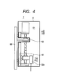
- FIG. 4 shows the basic configuration of a Z-direction reaction absorber equivalent to a second embodiment of the present invention
- FIG. 5 shows the basic configuration of a reaction absorber equivalent to a third embodiment of the present invention
- FIG. 6 shows the basic configuration of a reaction absorber equivalent to a fourth embodiment of the present invention.
- FIG. 7 shows a reaction absorber in the related art.
- FIG. 3 is a schematic top view showing the die bonder 10 equivalents to one embodiment of the present invention and also shows the details of a bonding head device 32 .
- the die bonder is roughly provided with a wafer supply unit 1 , a workpiece supplying/feeding unit 2 and a die bonding unit 3 .
- the wafer supply unit 1 is provided with a wafer cassette lifter 11 and a wafer ring holder 12 .
- the wafer cassette lifter 11 is provided with a wafer cassette (not shown) filled with wafer rings and supplies a wafer ring to the wafer ring holder 12 .
- the wafer ring holder 12 stretches a wafer tape that is held by the wafer ring downward to widen an interval between dies, helping the down side of a die be thrust up a die from the downside of the die by a thrusting unit, thus enhances the pickup performance of the die in a bonding process described later.
- the wafer ring holder 12 is arranged on an X-Y direct acting table, directly moves to the next die position after pickup, to be ready for the next pickup.
- the workpiece supplying/feeding unit 2 is provided with a stack loader 21 , a frame feeder 22 and an unloader 23 .
- a workpiece (a lead frame) supplied to the frame feeder 22 by the stack loader 21 is fed to the unloader 23 via two processing positions on the frame feeder 22 .
- the die bonding unit 3 is provided with a preformer 31 and the bonding head device 32 .
- the preformer 31 applies a die adhesive to the workpiece fed by the frame feeder 22 .
- the bonding head device 32 picks up the die from the wafer ring holder 12 , raises it, moves it in horizontally, and moves it to the bonding point on the frame feeder 22 .
- the bonding head device 32 lowers the die and bonds it onto the workpiece to which the die adhesive is applied.
- the bonding head device 32 is provided with an X-direction reaction absorber 6 that moves a bonding head (see 32 a in FIG. 4 ) between a pickup position in the wafer ring holder 12 and the bonding point, that is, in an X direction and a Z-direction reaction absorber 7 that is fixed to the X-direction reaction absorber 6 (that functions as a load) and moves the bonding head 32 a vertically (in a Z direction).
- FIG. 1 shows the basic configuration of the X-direction reaction absorber 6 equivalent to the first embodiment.
- FIG. 2 shows a state in which a load unit 62 that fixes the Z-direction reaction absorber 7 is moved rightward.
- the X-direction reaction absorber 6 is roughly provided with the load unit 62 which is an object of movement and which is shown inside a broken line, a driving unit 61 that laterally moves the load unit as shown by arrows in FIG. 1 , a reaction absorbing unit 63 that functions as a counter for reducing vibration by the load unit and a unit base 64 that supports or fixes these.
- the driving unit 61 is provided with a ball screw 61 a on the load side that moves the load unit 62 , a ball screw 61 b on the reaction absorption side coupled to the ball screw 61 a on the load side via a coupler 61 f for moving the reaction absorbing unit 63 , a driving motor 61 c (power source) that rotates both ball screws, a U-shaped driving fixed plate 61 d that supports the driving motor and both ball screws and a base guide 61 e that enables the driving fixed plate to move on the unit base 64 .
- a ball screw 61 a on the load side that moves the load unit 62
- a ball screw 61 b on the reaction absorption side coupled to the ball screw 61 a on the load side via a coupler 61 f for moving the reaction absorbing unit 63
- a driving motor 61 c power source
- U-shaped driving fixed plate 61 d that supports the driving motor and both ball screws
- a base guide 61 e that
- the load unit 62 is provided with a load fixing base 62 a that fixes or supports the reaction absorber 7 which is equipped with the bonding head 32 a (see FIG. 4 ) at an end and which functions as a load, a load nut 62 b fixed to the load fixing base and moved on the ball screw on the load side and a load guide 62 c that makes the load unit 62 smoothly moved over the driving fixed plate 61 d by the load nut.
- the load unit 62 is laterally moved by the rotation of the ball screw 61 a on the load side as shown by the arrows in FIG. 1 .
- the reaction absorbing unit 63 is provided with a reaction absorption nut 63 a (a supporting member) moved on the ball screw 61 b on the reaction absorption side on the side of one end and reaction absorbent 63 b (a support) fixed to the unit base 64 on the side of the other end.
- the unit base 64 is fixed to the bonding head device 32 and fixes the reaction absorbing unit 63 as described above. Further, the unit base supports a counter mechanism 8 provided with the driving unit 61 and the load unit 62 respectively shown inside a thick line movably in directions shown by the arrows by the base guide 61 e.
- FIG. 2 shows an example of the operation of the reaction absorber 6 provided with the above-mentioned configuration.
- FIG. 2 shows the example that the load unit 62 is moved rightward as shown by an arrow A by sequentially rotating the ball screw 61 a on the load side and the ball screw 61 b on the reaction absorption side in the same direction.
- the load unit is moved leftward, reverse operation is executed as shown in parentheses.
- the load unit 62 is moved rightward (leftward) by the rotation of the ball screw 61 a on the load side and the ball screw 61 b on the reaction absorption side and the reaction absorbing unit 63 also tries to move rightward (leftward).
- the reaction absorbing unit 63 is fixed to the unit base 64 , reactive force is conversely applied to the ball screw 61 b on the reaction absorption side and the ball screw on the reaction absorption side is moved leftward as shown by an arrow C for the unit base 64 .
- the counter mechanism 8 shown inside the thick line is moved over the unit base 64 by the base guide 61 e leftward (rightward) as shown by an arrow B.
- the load unit 62 also tries to move leftward (rightward) according to the movement of the driving unit 61 .
- the load unit 62 is moved rightward (leftward) as shown by the arrow A.
- a sufficient operational range can be acquired by setting the ratio R of the leads shown in the expression (1) to an appropriate value.
- the counter mechanism 8 shown inside the thick line in FIG. 2 and provided with the driving unit 61 and the load unit 62 functions as a counter load moved in a reverse direction to the load unit 62 . That is, the mass Km of the counter mechanism 8 which accounts for the substantial whole of the reaction absorber functions as the counter load that absorbs the vibration.
- M the ratio of the mass Km and the mass Fm of the load unit 62 shown inside the broken line
- the vibration is better offset as the ratio M:R of M to the lead ratio R shown in the expression (1) comes closer to 1.
- the ratio of M:R is in a range of 0.95 to 1.05.
- the ball screw 61 a on the load side and the ball screw 61 b on the reaction absorption side are rotated in the same direction. However, they may also be rotated in reverse directions.
- reverse vibration against vibration caused by the load unit is generated by the reaction absorbing unit and the vibration in operation can be reduced or offset.
- mass as a counter is not required to be added and the reaction absorber can be made light and compact. As a result, the driving of the reaction absorber can be sped up.
- reaction absorber can be made light and compact, time until the vibration is reduced or offset can be reduced and cycle time can be sped up. Since the time until the vibration is reduced or offset is short, the bonding head can execute the next process after the vibration is offset without sacrificing the cycle time and therefore, the quality can be enhanced.
- FIG. 4 shows the basic configuration of a Z-direction reaction absorber 7 equivalent to a second embodiment of the present invention.
- the Z-direction reaction absorber 7 is provided with a function for suctioning a die with a bonding head 32 a and for raising/lowering the die for bonding.
- the basic configuration of the Z-direction reaction absorber 7 is basically the same as that in the first embodiment shown in FIG. 1 . However, the Z-direction reaction absorber has some different points.
- the second embodiment will be described based upon the different points below.
- the same reference numeral is allocated to a part having the same function as the part in the first embodiment.
- a load in the second embodiment is the bonding head that raises/lowers an end of the Z-direction reaction absorber.
- a load unit 62 provided with the bonding head is provided on the side of a pointed end and a reaction absorbing unit 63 is provided in the vicinity of a driving motor 61 c at the base so as to facilitate raising/lowering the bonding head 32 a , suctioning a die and bonding the die.
- a unit base 65 of the Z-direction reaction absorber 7 is equivalent to the load fixing base 62 a of the X-direction reaction absorber 6 or is fixed to the load fixing base 62 a.
- FIG. 4 the inside of a thick black line shows a counter mechanism 8 which functions as a counter load and which is provided with the driving unit 61 and the load unit 62 , and the inside of a broken line shows the load unit 62 .
- vibration in a reverse direction against vibration caused by the load unit is generated by the reaction absorbing unit and the vibration in operation can also be reduced or offset.
- mass as a counter is not required to be added and the reaction absorber can be made light and compact. As a result, the driving of the reaction absorber can be sped up.
- the Z-direction reaction absorber can be made light and compact
- the X-direction reaction absorber 6 described in the first embodiment can be made lighter and more compact and the whole bonding head device 32 can be made light and compact.
- the throughput is enhanced because waiting time and low-speed driving time respectively in die bonding can be reduced by applying the direct acting bonding head device having degrees of freedom in two directions of the X direction and the Z direction described in the embodiments of the present invention to the die bonder 10 shown in FIG. 3 . Further, since the vibration in die bonding can be reduced, the quality of a product, particularly die bonding precision, is enhanced.
- a preforming head device directly acts with degrees of freedom in the two directions of the X direction and the Z direction and a wafer ring holder directly acts with degrees of freedom in two directions of the X direction and a Y direction.
- X, Y and Z are reference signs allocated to facilitate the understanding of the description and the reference numerals themselves have no meaning.
- the throughput is enhanced because waiting time and low-speed driving time respectively in die bonding can be further reduced when the above-mentioned reaction absorber according to the present invention is also applied to the preforming head and the wafer ring holder. Further, since vibration in die bonding can be reduced, the quality of a product, particularly die bonding precision is further enhanced.
- FIG. 5 shows a reaction absorber 9 equivalent to a third embodiment which can be applied to the X-direction reaction absorber 6 and the Z-direction reaction absorber 7 .
- the basic operation and the basic configuration in the third embodiment are the same as those of the first and second embodiments.
- the third embodiment will be described in relation to points different from those in the first and second embodiments below.
- a ball screw 61 a on the load side and a ball screw 61 b on the reaction absorption side are not aligned and are arranged in parallel.
- the driving force of a driving motor 61 c is transmitted to the ball screw 61 b on the reaction absorption side via gears 61 f 1 , 61 f 2 . Since the driving force is transmitted via the gears, threads of the ball screw 61 a on the load side and the ball screw 61 b on the reaction absorption side are cut in reverse directions.
- a reaction absorbing unit 63 tries to move in the same direction as a load unit 62 .
- reaction absorbing unit 63 is fixed to a unit base 64 , the reaction absorbing unit is moved in a reverse direction to the load unit 62 based upon the unit base 64 .
- a counter mechanism 8 shown inside a thick line is also moved in the reverse direction to the load unit 62 over the unit base 64 by a base guide 61 e.
- the driving force is transmitted via the gears.
- the similar operation to the operation shown in FIG. 5 is acquired by cutting the threads in the same direction.
- vibration in a reverse direction against vibration caused by the load unit 62 is also generated by the reaction absorbing unit 63 by making the counter mechanism 8 function as a counter load and the vibration in the operation can be reduced or offset.
- a reaction absorber can be made light and compact. As a result, the driving of the reaction absorber can be sped up.
- the load unit 62 and the reaction absorbing unit 63 are arranged vertically in the drawing based upon the unit base 64 . As a result, the length of the movement of the reaction absorbing unit can be reduced.
- the arrangement is not limited to that shown in FIG. 5 and for example, the load unit 62 and the reaction absorbing unit 63 may also be arranged in a direction of the depth of the drawing over the unit base 64 .
- the die bonder has been described as an example of the semiconductor assembling system. However, the present invention can also be applied to another semiconductor assembling system in which a processing head is operated at high speed.
- FIG. 6 shows a reaction absorber 5 equivalent to a fourth embodiment.
- a ball screw 61 b on the reaction absorption side is arranged on the left side of a driving motor 61 c and a ball screw 61 a on the load side is arranged on the right side of the driving motor 61 c .
- the driving motor 61 c , the ball screw 61 a on the load side and the ball screw 61 b on the reaction absorption side are aligned to make each rotational center of the motor 61 c , the ball screw 61 a on the load side and the ball screw 61 b on the reaction absorption side matched.
- Each one end of the ball screw 61 a on the load side and the ball screw 61 b on the reaction absorption side is rotatably supported by a driving fixed plate 61 d.
- the basic operation is the same as that in the first and second embodiments.
- the embodiments of the present invention have been described.
- the present invention includes various alternative examples, modification or transformation in a range not deviating from its object.
Applications Claiming Priority (2)
| Application Number | Priority Date | Filing Date | Title |
|---|---|---|---|
| JP2010-100049 | 2010-04-23 | ||
| JP2010100049A JP2011233578A (ja) | 2010-04-23 | 2010-04-23 | 反動吸収装置及び半導体組立装置 |
Publications (2)
| Publication Number | Publication Date |
|---|---|
| US20110259525A1 US20110259525A1 (en) | 2011-10-27 |
| US9177937B2 true US9177937B2 (en) | 2015-11-03 |
Family
ID=44814779
Family Applications (1)
| Application Number | Title | Priority Date | Filing Date |
|---|---|---|---|
| US12/880,399 Active 2032-04-01 US9177937B2 (en) | 2010-04-23 | 2010-09-13 | Reaction absorber and semiconductor assembling system |
Country Status (5)
| Country | Link |
|---|---|
| US (1) | US9177937B2 (ja) |
| JP (1) | JP2011233578A (ja) |
| KR (1) | KR101224264B1 (ja) |
| CN (1) | CN102235459B (ja) |
| TW (1) | TWI418718B (ja) |
Cited By (1)
| Publication number | Priority date | Publication date | Assignee | Title |
|---|---|---|---|---|
| US20230287952A1 (en) * | 2022-03-10 | 2023-09-14 | Taiwan Semiconductor Manufacturing Company, Ltd. | Systems and methods for reducing vibration of apparatuses |
Families Citing this family (11)
| Publication number | Priority date | Publication date | Assignee | Title |
|---|---|---|---|---|
| JP2011233578A (ja) * | 2010-04-23 | 2011-11-17 | Hitachi High-Tech Instruments Co Ltd | 反動吸収装置及び半導体組立装置 |
| JP5941705B2 (ja) * | 2012-02-29 | 2016-06-29 | ファスフォードテクノロジ株式会社 | 2軸駆動機構及びダイボンダ |
| JP2014056979A (ja) * | 2012-09-13 | 2014-03-27 | Hitachi High-Tech Instruments Co Ltd | 水平軸駆動機構、2軸駆動機構及びダイボンダ |
| KR101438639B1 (ko) * | 2013-07-09 | 2014-09-05 | 현대자동차 주식회사 | 차량용 도어 장착기의 도어 정위치 장치 |
| JP6276545B2 (ja) * | 2013-09-18 | 2018-02-07 | ファスフォードテクノロジ株式会社 | ダイボンダ |
| JP6573813B2 (ja) | 2015-09-30 | 2019-09-11 | ファスフォードテクノロジ株式会社 | ダイボンダおよび半導体装置の製造方法 |
| TWI580526B (zh) * | 2015-11-12 | 2017-05-01 | 財團法人工業技術研究院 | 減震裝置及其所使用之硏磨減震模組與滾刀減震模組 |
| CN106624950A (zh) * | 2016-12-07 | 2017-05-10 | 东莞市埃弗米数控设备科技有限公司 | 一种车刀架微动进给装置 |
| US10381321B2 (en) * | 2017-02-18 | 2019-08-13 | Kulicke And Soffa Industries, Inc | Ultrasonic transducer systems including tuned resonators, equipment including such systems, and methods of providing the same |
| TWI784622B (zh) * | 2020-08-12 | 2022-11-21 | 日商捷進科技有限公司 | 黏晶裝置及半導體裝置的製造方法 |
| CN112018003B (zh) * | 2020-09-02 | 2021-05-04 | 深圳新益昌科技股份有限公司 | 自动共晶机及共晶方法 |
Citations (13)
| Publication number | Priority date | Publication date | Assignee | Title |
|---|---|---|---|---|
| JPH01193134A (ja) | 1988-01-27 | 1989-08-03 | Komatsu Ltd | スライドテーブルを有する構造物のカウンターバランス移動装置 |
| JP2000150581A (ja) * | 1998-11-10 | 2000-05-30 | Hitachi Ltd | 半導体装置およびその製造方法並びにそれに使用されるボンディング装置 |
| JP2000340606A (ja) * | 1999-05-31 | 2000-12-08 | Hitachi Ltd | 半導体装置の製造方法およびそれを用いた半導体製造装置 |
| JP2000353720A (ja) * | 1999-06-09 | 2000-12-19 | Hitachi Ltd | 半導体装置の製造方法およびそれに使用されるワイヤボンディング装置 |
| JP2002118142A (ja) * | 2000-10-05 | 2002-04-19 | Hitachi Ltd | 半導体装置の製造方法および半導体製造装置 |
| JP2003332359A (ja) * | 2002-05-15 | 2003-11-21 | Renesas Technology Corp | 半導体装置の製造方法および半導体製造装置 |
| JP2004263825A (ja) | 2003-03-04 | 2004-09-24 | Nec Machinery Corp | 反力減衰駆動装置 |
| EP1724054A1 (en) * | 2005-05-18 | 2006-11-22 | Franco Sartorio | Counterbalance moving device for a machine tool |
| JP2007317748A (ja) * | 2006-05-23 | 2007-12-06 | Renesas Technology Corp | 半導体装置の製造方法 |
| JP2008066452A (ja) * | 2006-09-06 | 2008-03-21 | Renesas Technology Corp | 半導体装置の製造方法 |
| JP2009093536A (ja) * | 2007-10-11 | 2009-04-30 | Yokogawa Electric Corp | データ転送装置及び半導体試験装置 |
| JP2010073113A (ja) * | 2008-09-22 | 2010-04-02 | Yokogawa Electric Corp | データ転送装置及び半導体試験装置 |
| CN102235459A (zh) * | 2010-04-23 | 2011-11-09 | 株式会社日立高新技术仪器 | 反动吸收装置和半导体装配装置 |
Family Cites Families (3)
| Publication number | Priority date | Publication date | Assignee | Title |
|---|---|---|---|---|
| JP2808677B2 (ja) * | 1989-06-20 | 1998-10-08 | 株式会社ニコン | ステージ駆動方法 |
| JP2002198282A (ja) * | 2000-12-25 | 2002-07-12 | Nikon Corp | ステージ装置及びそれを有する露光装置 |
| KR101287526B1 (ko) * | 2005-03-15 | 2013-07-19 | 삼성전자주식회사 | 다이 본더와 이를 이용한 다이 본딩 방법 |
-
2010
- 2010-04-23 JP JP2010100049A patent/JP2011233578A/ja active Pending
- 2010-09-03 KR KR1020100086229A patent/KR101224264B1/ko active IP Right Grant
- 2010-09-10 CN CN201010279447.9A patent/CN102235459B/zh active Active
- 2010-09-10 TW TW099130661A patent/TWI418718B/zh active
- 2010-09-13 US US12/880,399 patent/US9177937B2/en active Active
Patent Citations (14)
| Publication number | Priority date | Publication date | Assignee | Title |
|---|---|---|---|---|
| JPH01193134A (ja) | 1988-01-27 | 1989-08-03 | Komatsu Ltd | スライドテーブルを有する構造物のカウンターバランス移動装置 |
| JP2000150581A (ja) * | 1998-11-10 | 2000-05-30 | Hitachi Ltd | 半導体装置およびその製造方法並びにそれに使用されるボンディング装置 |
| JP2000340606A (ja) * | 1999-05-31 | 2000-12-08 | Hitachi Ltd | 半導体装置の製造方法およびそれを用いた半導体製造装置 |
| JP2000353720A (ja) * | 1999-06-09 | 2000-12-19 | Hitachi Ltd | 半導体装置の製造方法およびそれに使用されるワイヤボンディング装置 |
| JP2002118142A (ja) * | 2000-10-05 | 2002-04-19 | Hitachi Ltd | 半導体装置の製造方法および半導体製造装置 |
| JP2003332359A (ja) * | 2002-05-15 | 2003-11-21 | Renesas Technology Corp | 半導体装置の製造方法および半導体製造装置 |
| JP2004263825A (ja) | 2003-03-04 | 2004-09-24 | Nec Machinery Corp | 反力減衰駆動装置 |
| EP1724054A1 (en) * | 2005-05-18 | 2006-11-22 | Franco Sartorio | Counterbalance moving device for a machine tool |
| JP2007317748A (ja) * | 2006-05-23 | 2007-12-06 | Renesas Technology Corp | 半導体装置の製造方法 |
| JP2008066452A (ja) * | 2006-09-06 | 2008-03-21 | Renesas Technology Corp | 半導体装置の製造方法 |
| JP2009093536A (ja) * | 2007-10-11 | 2009-04-30 | Yokogawa Electric Corp | データ転送装置及び半導体試験装置 |
| JP2010073113A (ja) * | 2008-09-22 | 2010-04-02 | Yokogawa Electric Corp | データ転送装置及び半導体試験装置 |
| CN102235459A (zh) * | 2010-04-23 | 2011-11-09 | 株式会社日立高新技术仪器 | 反动吸收装置和半导体装配装置 |
| JP2011233578A (ja) * | 2010-04-23 | 2011-11-17 | Hitachi High-Tech Instruments Co Ltd | 反動吸収装置及び半導体組立装置 |
Non-Patent Citations (7)
| Title |
|---|
| Chinese office action of dated Feb. 16, 2013. |
| English translation of EP1724054A1; Nov. 2006. * |
| English translation of JP 01-193134; Aug. 1999. * |
| English translation of JP 2002-118142; Mochizuki et al. Apr. 19, 2002. * |
| English translation of JP2002198282; Jul. 2002. * |
| English translation of JP2004-263825; Sueda. Sep. 24, 2004. * |
| Translation of Office Action for CN201010279447.9; Chinese Patent Office; Feb. 16, 2013. * |
Cited By (1)
| Publication number | Priority date | Publication date | Assignee | Title |
|---|---|---|---|---|
| US20230287952A1 (en) * | 2022-03-10 | 2023-09-14 | Taiwan Semiconductor Manufacturing Company, Ltd. | Systems and methods for reducing vibration of apparatuses |
Also Published As
| Publication number | Publication date |
|---|---|
| JP2011233578A (ja) | 2011-11-17 |
| US20110259525A1 (en) | 2011-10-27 |
| CN102235459B (zh) | 2015-06-03 |
| CN102235459A (zh) | 2011-11-09 |
| KR101224264B1 (ko) | 2013-01-18 |
| TWI418718B (zh) | 2013-12-11 |
| KR20110118549A (ko) | 2011-10-31 |
| TW201137262A (en) | 2011-11-01 |
Similar Documents
| Publication | Publication Date | Title |
|---|---|---|
| US9177937B2 (en) | Reaction absorber and semiconductor assembling system | |
| CN207494569U (zh) | 一种桁架式车床上下料机械手 | |
| CN114361076B (zh) | 全自动三极管clip组装线 | |
| KR100394127B1 (ko) | 다이 및 소형 부품의 이송 장치 | |
| CN208368539U (zh) | 一种宽支架led固晶装置 | |
| US7320424B2 (en) | Linear split axis wire bonder | |
| CN212542373U (zh) | 多芯片智能贴装设备 | |
| CN103295932B (zh) | 双轴驱动机构及芯片接合机 | |
| CN106876307B (zh) | 垂直取晶、固晶机构及其采用它的垂直固晶机 | |
| CN113501159A (zh) | 一种避免芯片损伤供料的芯片编带机 | |
| CN112536470A (zh) | 一种精密金属组件的高效切割装置 | |
| US7320423B2 (en) | High speed linear and rotary split-axis wire bonder | |
| JP5410625B2 (ja) | 反動吸収装置及び半導体組立装置 | |
| CN210805707U (zh) | 一种多工位多芯片的半导体封装设备 | |
| CN213954104U (zh) | 一种半导体基础材料自动粘接系统 | |
| CN212705361U (zh) | 一种变速控制器全自动螺钉装配装置 | |
| CN113479371A (zh) | 一种非振动供料的芯片编带机 | |
| CN114267611A (zh) | 一种led封装设备 | |
| CN115709142A (zh) | 一种半导体贴装机 | |
| JP2003136163A (ja) | トランスファプレスのワーク搬送方法及びワーク搬送装置 | |
| CN219759536U (zh) | 一种环形固晶机 | |
| CN218841010U (zh) | 一种芯片上料输送模块 | |
| CN218274551U (zh) | 芯片位置修正机构和半导体贴片封装机 | |
| CN210614190U (zh) | 一种蓝牙耳机pcba板的涂胶设备 | |
| CN217650379U (zh) | 一种转盘式芯片分选机铁片输送机构 |
Legal Events
| Date | Code | Title | Description |
|---|---|---|---|
| AS | Assignment |
Owner name: HITACHI HIGH-TECH INSTRUMENTS CO., LTD., JAPAN Free format text: ASSIGNMENT OF ASSIGNORS INTEREST;ASSIGNORS:MOCHIZUKI, MASAYUKI;ISHII, YASUSHI;REEL/FRAME:025391/0741 Effective date: 20100914 |
|
| AS | Assignment |
Owner name: FASFORD TECHNOLOGY CO., LTD., JAPAN Free format text: ASSIGNMENT OF ASSIGNORS INTEREST;ASSIGNOR:HITACHI HIGH-TECH INSTRUMENTS CO., LTD.;REEL/FRAME:035753/0236 Effective date: 20150525 |
|
| STCF | Information on status: patent grant |
Free format text: PATENTED CASE |
|
| MAFP | Maintenance fee payment |
Free format text: PAYMENT OF MAINTENANCE FEE, 4TH YEAR, LARGE ENTITY (ORIGINAL EVENT CODE: M1551); ENTITY STATUS OF PATENT OWNER: LARGE ENTITY Year of fee payment: 4 |
|
| MAFP | Maintenance fee payment |
Free format text: PAYMENT OF MAINTENANCE FEE, 8TH YEAR, LARGE ENTITY (ORIGINAL EVENT CODE: M1552); ENTITY STATUS OF PATENT OWNER: LARGE ENTITY Year of fee payment: 8 |