KR20150014867A - 반도체 장치 및 그 제조 방법 - Google Patents
반도체 장치 및 그 제조 방법 Download PDFInfo
- Publication number
- KR20150014867A KR20150014867A KR1020140094613A KR20140094613A KR20150014867A KR 20150014867 A KR20150014867 A KR 20150014867A KR 1020140094613 A KR1020140094613 A KR 1020140094613A KR 20140094613 A KR20140094613 A KR 20140094613A KR 20150014867 A KR20150014867 A KR 20150014867A
- Authority
- KR
- South Korea
- Prior art keywords
- bonding
- terminals
- wire
- semiconductor chip
- wires
- Prior art date
Links
- 239000004065 semiconductor Substances 0.000 title claims abstract description 238
- 238000004519 manufacturing process Methods 0.000 title abstract description 5
- 239000000758 substrate Substances 0.000 claims abstract description 32
- 238000000034 method Methods 0.000 claims description 126
- 230000002708 enhancing effect Effects 0.000 abstract 1
- 239000000463 material Substances 0.000 description 55
- 229910000679 solder Inorganic materials 0.000 description 40
- 238000007789 sealing Methods 0.000 description 21
- 239000010410 layer Substances 0.000 description 20
- PXHVJJICTQNCMI-UHFFFAOYSA-N Nickel Chemical compound [Ni] PXHVJJICTQNCMI-UHFFFAOYSA-N 0.000 description 14
- 239000000853 adhesive Substances 0.000 description 13
- 230000001070 adhesive effect Effects 0.000 description 13
- 239000010949 copper Substances 0.000 description 13
- 229910052751 metal Inorganic materials 0.000 description 13
- 239000002184 metal Substances 0.000 description 13
- 229920005989 resin Polymers 0.000 description 13
- 239000011347 resin Substances 0.000 description 13
- 238000012986 modification Methods 0.000 description 12
- 230000004048 modification Effects 0.000 description 12
- 239000010931 gold Substances 0.000 description 9
- RYGMFSIKBFXOCR-UHFFFAOYSA-N Copper Chemical compound [Cu] RYGMFSIKBFXOCR-UHFFFAOYSA-N 0.000 description 7
- 229910052802 copper Inorganic materials 0.000 description 7
- PCHJSUWPFVWCPO-UHFFFAOYSA-N gold Chemical compound [Au] PCHJSUWPFVWCPO-UHFFFAOYSA-N 0.000 description 6
- 229910052737 gold Inorganic materials 0.000 description 6
- 229910052759 nickel Inorganic materials 0.000 description 6
- XUIMIQQOPSSXEZ-UHFFFAOYSA-N Silicon Chemical compound [Si] XUIMIQQOPSSXEZ-UHFFFAOYSA-N 0.000 description 5
- 239000011159 matrix material Substances 0.000 description 5
- 229910052710 silicon Inorganic materials 0.000 description 5
- 239000010703 silicon Substances 0.000 description 5
- 235000012431 wafers Nutrition 0.000 description 5
- 238000013461 design Methods 0.000 description 4
- 238000007747 plating Methods 0.000 description 4
- 238000013459 approach Methods 0.000 description 3
- 238000002360 preparation method Methods 0.000 description 3
- 238000003825 pressing Methods 0.000 description 3
- 230000000630 rising effect Effects 0.000 description 3
- 229910000577 Silicon-germanium Inorganic materials 0.000 description 2
- 229910045601 alloy Inorganic materials 0.000 description 2
- 239000000956 alloy Substances 0.000 description 2
- 238000005452 bending Methods 0.000 description 2
- 238000010586 diagram Methods 0.000 description 2
- 238000009713 electroplating Methods 0.000 description 2
- 230000012447 hatching Effects 0.000 description 2
- 238000000465 moulding Methods 0.000 description 2
- 239000004033 plastic Substances 0.000 description 2
- 229910017944 Ag—Cu Inorganic materials 0.000 description 1
- 229920000049 Carbon (fiber) Polymers 0.000 description 1
- 229910000881 Cu alloy Inorganic materials 0.000 description 1
- ATJFFYVFTNAWJD-UHFFFAOYSA-N Tin Chemical compound [Sn] ATJFFYVFTNAWJD-UHFFFAOYSA-N 0.000 description 1
- LEVVHYCKPQWKOP-UHFFFAOYSA-N [Si].[Ge] Chemical compound [Si].[Ge] LEVVHYCKPQWKOP-UHFFFAOYSA-N 0.000 description 1
- 239000000654 additive Substances 0.000 description 1
- 238000004026 adhesive bonding Methods 0.000 description 1
- 239000012790 adhesive layer Substances 0.000 description 1
- 229910052782 aluminium Inorganic materials 0.000 description 1
- XAGFODPZIPBFFR-UHFFFAOYSA-N aluminium Chemical compound [Al] XAGFODPZIPBFFR-UHFFFAOYSA-N 0.000 description 1
- 230000005540 biological transmission Effects 0.000 description 1
- 230000015572 biosynthetic process Effects 0.000 description 1
- JWVAUCBYEDDGAD-UHFFFAOYSA-N bismuth tin Chemical compound [Sn].[Bi] JWVAUCBYEDDGAD-UHFFFAOYSA-N 0.000 description 1
- 238000005219 brazing Methods 0.000 description 1
- 239000004917 carbon fiber Substances 0.000 description 1
- 239000000470 constituent Substances 0.000 description 1
- 238000005520 cutting process Methods 0.000 description 1
- 238000007599 discharging Methods 0.000 description 1
- 239000003822 epoxy resin Substances 0.000 description 1
- 239000003365 glass fiber Substances 0.000 description 1
- 239000000383 hazardous chemical Substances 0.000 description 1
- 238000010438 heat treatment Methods 0.000 description 1
- 238000007689 inspection Methods 0.000 description 1
- 238000010030 laminating Methods 0.000 description 1
- 125000005647 linker group Chemical group 0.000 description 1
- 239000007769 metal material Substances 0.000 description 1
- VNWKTOKETHGBQD-UHFFFAOYSA-N methane Chemical compound C VNWKTOKETHGBQD-UHFFFAOYSA-N 0.000 description 1
- 239000000203 mixture Substances 0.000 description 1
- 235000011837 pasties Nutrition 0.000 description 1
- 238000000059 patterning Methods 0.000 description 1
- 229920000647 polyepoxide Polymers 0.000 description 1
- 238000012545 processing Methods 0.000 description 1
- 238000002407 reforming Methods 0.000 description 1
- 230000003252 repetitive effect Effects 0.000 description 1
- 238000000926 separation method Methods 0.000 description 1
- 230000008054 signal transmission Effects 0.000 description 1
- 238000004513 sizing Methods 0.000 description 1
- 230000000087 stabilizing effect Effects 0.000 description 1
- 238000012360 testing method Methods 0.000 description 1
- 229920001187 thermosetting polymer Polymers 0.000 description 1
- 238000012546 transfer Methods 0.000 description 1
Images


Classifications
-
- H—ELECTRICITY
- H01—ELECTRIC ELEMENTS
- H01L—SEMICONDUCTOR DEVICES NOT COVERED BY CLASS H10
- H01L23/00—Details of semiconductor or other solid state devices
- H01L23/48—Arrangements for conducting electric current to or from the solid state body in operation, e.g. leads, terminal arrangements ; Selection of materials therefor
- H01L23/488—Arrangements for conducting electric current to or from the solid state body in operation, e.g. leads, terminal arrangements ; Selection of materials therefor consisting of soldered or bonded constructions
- H01L23/498—Leads, i.e. metallisations or lead-frames on insulating substrates, e.g. chip carriers
- H01L23/49811—Additional leads joined to the metallisation on the insulating substrate, e.g. pins, bumps, wires, flat leads
-
- H—ELECTRICITY
- H01—ELECTRIC ELEMENTS
- H01L—SEMICONDUCTOR DEVICES NOT COVERED BY CLASS H10
- H01L23/00—Details of semiconductor or other solid state devices
- H01L23/48—Arrangements for conducting electric current to or from the solid state body in operation, e.g. leads, terminal arrangements ; Selection of materials therefor
- H01L23/488—Arrangements for conducting electric current to or from the solid state body in operation, e.g. leads, terminal arrangements ; Selection of materials therefor consisting of soldered or bonded constructions
- H01L23/498—Leads, i.e. metallisations or lead-frames on insulating substrates, e.g. chip carriers
- H01L23/49827—Via connections through the substrates, e.g. pins going through the substrate, coaxial cables
-
- H—ELECTRICITY
- H01—ELECTRIC ELEMENTS
- H01L—SEMICONDUCTOR DEVICES NOT COVERED BY CLASS H10
- H01L23/00—Details of semiconductor or other solid state devices
- H01L23/48—Arrangements for conducting electric current to or from the solid state body in operation, e.g. leads, terminal arrangements ; Selection of materials therefor
- H01L23/488—Arrangements for conducting electric current to or from the solid state body in operation, e.g. leads, terminal arrangements ; Selection of materials therefor consisting of soldered or bonded constructions
- H01L23/498—Leads, i.e. metallisations or lead-frames on insulating substrates, e.g. chip carriers
- H01L23/49838—Geometry or layout
-
- H—ELECTRICITY
- H01—ELECTRIC ELEMENTS
- H01L—SEMICONDUCTOR DEVICES NOT COVERED BY CLASS H10
- H01L24/00—Arrangements for connecting or disconnecting semiconductor or solid-state bodies; Methods or apparatus related thereto
- H01L24/01—Means for bonding being attached to, or being formed on, the surface to be connected, e.g. chip-to-package, die-attach, "first-level" interconnects; Manufacturing methods related thereto
- H01L24/02—Bonding areas ; Manufacturing methods related thereto
- H01L24/04—Structure, shape, material or disposition of the bonding areas prior to the connecting process
- H01L24/06—Structure, shape, material or disposition of the bonding areas prior to the connecting process of a plurality of bonding areas
-
- H—ELECTRICITY
- H01—ELECTRIC ELEMENTS
- H01L—SEMICONDUCTOR DEVICES NOT COVERED BY CLASS H10
- H01L24/00—Arrangements for connecting or disconnecting semiconductor or solid-state bodies; Methods or apparatus related thereto
- H01L24/01—Means for bonding being attached to, or being formed on, the surface to be connected, e.g. chip-to-package, die-attach, "first-level" interconnects; Manufacturing methods related thereto
- H01L24/42—Wire connectors; Manufacturing methods related thereto
- H01L24/47—Structure, shape, material or disposition of the wire connectors after the connecting process
- H01L24/49—Structure, shape, material or disposition of the wire connectors after the connecting process of a plurality of wire connectors
-
- H—ELECTRICITY
- H01—ELECTRIC ELEMENTS
- H01L—SEMICONDUCTOR DEVICES NOT COVERED BY CLASS H10
- H01L24/00—Arrangements for connecting or disconnecting semiconductor or solid-state bodies; Methods or apparatus related thereto
- H01L24/80—Methods for connecting semiconductor or other solid state bodies using means for bonding being attached to, or being formed on, the surface to be connected
- H01L24/85—Methods for connecting semiconductor or other solid state bodies using means for bonding being attached to, or being formed on, the surface to be connected using a wire connector
-
- H—ELECTRICITY
- H01—ELECTRIC ELEMENTS
- H01L—SEMICONDUCTOR DEVICES NOT COVERED BY CLASS H10
- H01L24/00—Arrangements for connecting or disconnecting semiconductor or solid-state bodies; Methods or apparatus related thereto
- H01L24/93—Batch processes
- H01L24/95—Batch processes at chip-level, i.e. with connecting carried out on a plurality of singulated devices, i.e. on diced chips
- H01L24/97—Batch processes at chip-level, i.e. with connecting carried out on a plurality of singulated devices, i.e. on diced chips the devices being connected to a common substrate, e.g. interposer, said common substrate being separable into individual assemblies after connecting
-
- H—ELECTRICITY
- H01—ELECTRIC ELEMENTS
- H01L—SEMICONDUCTOR DEVICES NOT COVERED BY CLASS H10
- H01L25/00—Assemblies consisting of a plurality of individual semiconductor or other solid state devices ; Multistep manufacturing processes thereof
- H01L25/03—Assemblies consisting of a plurality of individual semiconductor or other solid state devices ; Multistep manufacturing processes thereof all the devices being of a type provided for in the same subgroup of groups H01L27/00 - H01L33/00, or in a single subclass of H10K, H10N, e.g. assemblies of rectifier diodes
- H01L25/04—Assemblies consisting of a plurality of individual semiconductor or other solid state devices ; Multistep manufacturing processes thereof all the devices being of a type provided for in the same subgroup of groups H01L27/00 - H01L33/00, or in a single subclass of H10K, H10N, e.g. assemblies of rectifier diodes the devices not having separate containers
- H01L25/065—Assemblies consisting of a plurality of individual semiconductor or other solid state devices ; Multistep manufacturing processes thereof all the devices being of a type provided for in the same subgroup of groups H01L27/00 - H01L33/00, or in a single subclass of H10K, H10N, e.g. assemblies of rectifier diodes the devices not having separate containers the devices being of a type provided for in group H01L27/00
- H01L25/0657—Stacked arrangements of devices
-
- H—ELECTRICITY
- H01—ELECTRIC ELEMENTS
- H01L—SEMICONDUCTOR DEVICES NOT COVERED BY CLASS H10
- H01L21/00—Processes or apparatus adapted for the manufacture or treatment of semiconductor or solid state devices or of parts thereof
- H01L21/02—Manufacture or treatment of semiconductor devices or of parts thereof
- H01L21/04—Manufacture or treatment of semiconductor devices or of parts thereof the devices having potential barriers, e.g. a PN junction, depletion layer or carrier concentration layer
- H01L21/50—Assembly of semiconductor devices using processes or apparatus not provided for in a single one of the subgroups H01L21/06 - H01L21/326, e.g. sealing of a cap to a base of a container
- H01L21/56—Encapsulations, e.g. encapsulation layers, coatings
- H01L21/561—Batch processing
-
- H—ELECTRICITY
- H01—ELECTRIC ELEMENTS
- H01L—SEMICONDUCTOR DEVICES NOT COVERED BY CLASS H10
- H01L2224/00—Indexing scheme for arrangements for connecting or disconnecting semiconductor or solid-state bodies and methods related thereto as covered by H01L24/00
- H01L2224/01—Means for bonding being attached to, or being formed on, the surface to be connected, e.g. chip-to-package, die-attach, "first-level" interconnects; Manufacturing methods related thereto
- H01L2224/02—Bonding areas; Manufacturing methods related thereto
- H01L2224/04—Structure, shape, material or disposition of the bonding areas prior to the connecting process
- H01L2224/04042—Bonding areas specifically adapted for wire connectors, e.g. wirebond pads
-
- H—ELECTRICITY
- H01—ELECTRIC ELEMENTS
- H01L—SEMICONDUCTOR DEVICES NOT COVERED BY CLASS H10
- H01L2224/00—Indexing scheme for arrangements for connecting or disconnecting semiconductor or solid-state bodies and methods related thereto as covered by H01L24/00
- H01L2224/01—Means for bonding being attached to, or being formed on, the surface to be connected, e.g. chip-to-package, die-attach, "first-level" interconnects; Manufacturing methods related thereto
- H01L2224/02—Bonding areas; Manufacturing methods related thereto
- H01L2224/04—Structure, shape, material or disposition of the bonding areas prior to the connecting process
- H01L2224/05—Structure, shape, material or disposition of the bonding areas prior to the connecting process of an individual bonding area
- H01L2224/05001—Internal layers
- H01L2224/05099—Material
- H01L2224/051—Material with a principal constituent of the material being a metal or a metalloid, e.g. boron [B], silicon [Si], germanium [Ge], arsenic [As], antimony [Sb], tellurium [Te] and polonium [Po], and alloys thereof
- H01L2224/05138—Material with a principal constituent of the material being a metal or a metalloid, e.g. boron [B], silicon [Si], germanium [Ge], arsenic [As], antimony [Sb], tellurium [Te] and polonium [Po], and alloys thereof the principal constituent melting at a temperature of greater than or equal to 950°C and less than 1550°C
- H01L2224/05147—Copper [Cu] as principal constituent
-
- H—ELECTRICITY
- H01—ELECTRIC ELEMENTS
- H01L—SEMICONDUCTOR DEVICES NOT COVERED BY CLASS H10
- H01L2224/00—Indexing scheme for arrangements for connecting or disconnecting semiconductor or solid-state bodies and methods related thereto as covered by H01L24/00
- H01L2224/01—Means for bonding being attached to, or being formed on, the surface to be connected, e.g. chip-to-package, die-attach, "first-level" interconnects; Manufacturing methods related thereto
- H01L2224/02—Bonding areas; Manufacturing methods related thereto
- H01L2224/04—Structure, shape, material or disposition of the bonding areas prior to the connecting process
- H01L2224/05—Structure, shape, material or disposition of the bonding areas prior to the connecting process of an individual bonding area
- H01L2224/05001—Internal layers
- H01L2224/05099—Material
- H01L2224/051—Material with a principal constituent of the material being a metal or a metalloid, e.g. boron [B], silicon [Si], germanium [Ge], arsenic [As], antimony [Sb], tellurium [Te] and polonium [Po], and alloys thereof
- H01L2224/05138—Material with a principal constituent of the material being a metal or a metalloid, e.g. boron [B], silicon [Si], germanium [Ge], arsenic [As], antimony [Sb], tellurium [Te] and polonium [Po], and alloys thereof the principal constituent melting at a temperature of greater than or equal to 950°C and less than 1550°C
- H01L2224/05155—Nickel [Ni] as principal constituent
-
- H—ELECTRICITY
- H01—ELECTRIC ELEMENTS
- H01L—SEMICONDUCTOR DEVICES NOT COVERED BY CLASS H10
- H01L2224/00—Indexing scheme for arrangements for connecting or disconnecting semiconductor or solid-state bodies and methods related thereto as covered by H01L24/00
- H01L2224/01—Means for bonding being attached to, or being formed on, the surface to be connected, e.g. chip-to-package, die-attach, "first-level" interconnects; Manufacturing methods related thereto
- H01L2224/02—Bonding areas; Manufacturing methods related thereto
- H01L2224/04—Structure, shape, material or disposition of the bonding areas prior to the connecting process
- H01L2224/05—Structure, shape, material or disposition of the bonding areas prior to the connecting process of an individual bonding area
- H01L2224/0554—External layer
- H01L2224/0555—Shape
- H01L2224/05552—Shape in top view
- H01L2224/05553—Shape in top view being rectangular
-
- H—ELECTRICITY
- H01—ELECTRIC ELEMENTS
- H01L—SEMICONDUCTOR DEVICES NOT COVERED BY CLASS H10
- H01L2224/00—Indexing scheme for arrangements for connecting or disconnecting semiconductor or solid-state bodies and methods related thereto as covered by H01L24/00
- H01L2224/01—Means for bonding being attached to, or being formed on, the surface to be connected, e.g. chip-to-package, die-attach, "first-level" interconnects; Manufacturing methods related thereto
- H01L2224/02—Bonding areas; Manufacturing methods related thereto
- H01L2224/04—Structure, shape, material or disposition of the bonding areas prior to the connecting process
- H01L2224/05—Structure, shape, material or disposition of the bonding areas prior to the connecting process of an individual bonding area
- H01L2224/0554—External layer
- H01L2224/0555—Shape
- H01L2224/05552—Shape in top view
- H01L2224/05554—Shape in top view being square
-
- H—ELECTRICITY
- H01—ELECTRIC ELEMENTS
- H01L—SEMICONDUCTOR DEVICES NOT COVERED BY CLASS H10
- H01L2224/00—Indexing scheme for arrangements for connecting or disconnecting semiconductor or solid-state bodies and methods related thereto as covered by H01L24/00
- H01L2224/01—Means for bonding being attached to, or being formed on, the surface to be connected, e.g. chip-to-package, die-attach, "first-level" interconnects; Manufacturing methods related thereto
- H01L2224/02—Bonding areas; Manufacturing methods related thereto
- H01L2224/04—Structure, shape, material or disposition of the bonding areas prior to the connecting process
- H01L2224/05—Structure, shape, material or disposition of the bonding areas prior to the connecting process of an individual bonding area
- H01L2224/0554—External layer
- H01L2224/05599—Material
- H01L2224/056—Material with a principal constituent of the material being a metal or a metalloid, e.g. boron [B], silicon [Si], germanium [Ge], arsenic [As], antimony [Sb], tellurium [Te] and polonium [Po], and alloys thereof
- H01L2224/05617—Material with a principal constituent of the material being a metal or a metalloid, e.g. boron [B], silicon [Si], germanium [Ge], arsenic [As], antimony [Sb], tellurium [Te] and polonium [Po], and alloys thereof the principal constituent melting at a temperature of greater than or equal to 400°C and less than 950°C
- H01L2224/05624—Aluminium [Al] as principal constituent
-
- H—ELECTRICITY
- H01—ELECTRIC ELEMENTS
- H01L—SEMICONDUCTOR DEVICES NOT COVERED BY CLASS H10
- H01L2224/00—Indexing scheme for arrangements for connecting or disconnecting semiconductor or solid-state bodies and methods related thereto as covered by H01L24/00
- H01L2224/01—Means for bonding being attached to, or being formed on, the surface to be connected, e.g. chip-to-package, die-attach, "first-level" interconnects; Manufacturing methods related thereto
- H01L2224/02—Bonding areas; Manufacturing methods related thereto
- H01L2224/04—Structure, shape, material or disposition of the bonding areas prior to the connecting process
- H01L2224/05—Structure, shape, material or disposition of the bonding areas prior to the connecting process of an individual bonding area
- H01L2224/0554—External layer
- H01L2224/05599—Material
- H01L2224/056—Material with a principal constituent of the material being a metal or a metalloid, e.g. boron [B], silicon [Si], germanium [Ge], arsenic [As], antimony [Sb], tellurium [Te] and polonium [Po], and alloys thereof
- H01L2224/05638—Material with a principal constituent of the material being a metal or a metalloid, e.g. boron [B], silicon [Si], germanium [Ge], arsenic [As], antimony [Sb], tellurium [Te] and polonium [Po], and alloys thereof the principal constituent melting at a temperature of greater than or equal to 950°C and less than 1550°C
- H01L2224/05644—Gold [Au] as principal constituent
-
- H—ELECTRICITY
- H01—ELECTRIC ELEMENTS
- H01L—SEMICONDUCTOR DEVICES NOT COVERED BY CLASS H10
- H01L2224/00—Indexing scheme for arrangements for connecting or disconnecting semiconductor or solid-state bodies and methods related thereto as covered by H01L24/00
- H01L2224/01—Means for bonding being attached to, or being formed on, the surface to be connected, e.g. chip-to-package, die-attach, "first-level" interconnects; Manufacturing methods related thereto
- H01L2224/02—Bonding areas; Manufacturing methods related thereto
- H01L2224/04—Structure, shape, material or disposition of the bonding areas prior to the connecting process
- H01L2224/06—Structure, shape, material or disposition of the bonding areas prior to the connecting process of a plurality of bonding areas
- H01L2224/061—Disposition
- H01L2224/0612—Layout
-
- H—ELECTRICITY
- H01—ELECTRIC ELEMENTS
- H01L—SEMICONDUCTOR DEVICES NOT COVERED BY CLASS H10
- H01L2224/00—Indexing scheme for arrangements for connecting or disconnecting semiconductor or solid-state bodies and methods related thereto as covered by H01L24/00
- H01L2224/01—Means for bonding being attached to, or being formed on, the surface to be connected, e.g. chip-to-package, die-attach, "first-level" interconnects; Manufacturing methods related thereto
- H01L2224/26—Layer connectors, e.g. plate connectors, solder or adhesive layers; Manufacturing methods related thereto
- H01L2224/28—Structure, shape, material or disposition of the layer connectors prior to the connecting process
- H01L2224/29—Structure, shape, material or disposition of the layer connectors prior to the connecting process of an individual layer connector
- H01L2224/29001—Core members of the layer connector
- H01L2224/29099—Material
- H01L2224/2919—Material with a principal constituent of the material being a polymer, e.g. polyester, phenolic based polymer, epoxy
-
- H—ELECTRICITY
- H01—ELECTRIC ELEMENTS
- H01L—SEMICONDUCTOR DEVICES NOT COVERED BY CLASS H10
- H01L2224/00—Indexing scheme for arrangements for connecting or disconnecting semiconductor or solid-state bodies and methods related thereto as covered by H01L24/00
- H01L2224/01—Means for bonding being attached to, or being formed on, the surface to be connected, e.g. chip-to-package, die-attach, "first-level" interconnects; Manufacturing methods related thereto
- H01L2224/26—Layer connectors, e.g. plate connectors, solder or adhesive layers; Manufacturing methods related thereto
- H01L2224/31—Structure, shape, material or disposition of the layer connectors after the connecting process
- H01L2224/32—Structure, shape, material or disposition of the layer connectors after the connecting process of an individual layer connector
- H01L2224/321—Disposition
- H01L2224/32135—Disposition the layer connector connecting between different semiconductor or solid-state bodies, i.e. chip-to-chip
- H01L2224/32145—Disposition the layer connector connecting between different semiconductor or solid-state bodies, i.e. chip-to-chip the bodies being stacked
-
- H—ELECTRICITY
- H01—ELECTRIC ELEMENTS
- H01L—SEMICONDUCTOR DEVICES NOT COVERED BY CLASS H10
- H01L2224/00—Indexing scheme for arrangements for connecting or disconnecting semiconductor or solid-state bodies and methods related thereto as covered by H01L24/00
- H01L2224/01—Means for bonding being attached to, or being formed on, the surface to be connected, e.g. chip-to-package, die-attach, "first-level" interconnects; Manufacturing methods related thereto
- H01L2224/26—Layer connectors, e.g. plate connectors, solder or adhesive layers; Manufacturing methods related thereto
- H01L2224/31—Structure, shape, material or disposition of the layer connectors after the connecting process
- H01L2224/32—Structure, shape, material or disposition of the layer connectors after the connecting process of an individual layer connector
- H01L2224/321—Disposition
- H01L2224/32151—Disposition the layer connector connecting between a semiconductor or solid-state body and an item not being a semiconductor or solid-state body, e.g. chip-to-substrate, chip-to-passive
- H01L2224/32221—Disposition the layer connector connecting between a semiconductor or solid-state body and an item not being a semiconductor or solid-state body, e.g. chip-to-substrate, chip-to-passive the body and the item being stacked
- H01L2224/32225—Disposition the layer connector connecting between a semiconductor or solid-state body and an item not being a semiconductor or solid-state body, e.g. chip-to-substrate, chip-to-passive the body and the item being stacked the item being non-metallic, e.g. insulating substrate with or without metallisation
-
- H—ELECTRICITY
- H01—ELECTRIC ELEMENTS
- H01L—SEMICONDUCTOR DEVICES NOT COVERED BY CLASS H10
- H01L2224/00—Indexing scheme for arrangements for connecting or disconnecting semiconductor or solid-state bodies and methods related thereto as covered by H01L24/00
- H01L2224/01—Means for bonding being attached to, or being formed on, the surface to be connected, e.g. chip-to-package, die-attach, "first-level" interconnects; Manufacturing methods related thereto
- H01L2224/42—Wire connectors; Manufacturing methods related thereto
- H01L2224/44—Structure, shape, material or disposition of the wire connectors prior to the connecting process
- H01L2224/45—Structure, shape, material or disposition of the wire connectors prior to the connecting process of an individual wire connector
- H01L2224/45001—Core members of the connector
- H01L2224/45099—Material
- H01L2224/451—Material with a principal constituent of the material being a metal or a metalloid, e.g. boron (B), silicon (Si), germanium (Ge), arsenic (As), antimony (Sb), tellurium (Te) and polonium (Po), and alloys thereof
- H01L2224/45138—Material with a principal constituent of the material being a metal or a metalloid, e.g. boron (B), silicon (Si), germanium (Ge), arsenic (As), antimony (Sb), tellurium (Te) and polonium (Po), and alloys thereof the principal constituent melting at a temperature of greater than or equal to 950°C and less than 1550°C
- H01L2224/45144—Gold (Au) as principal constituent
-
- H—ELECTRICITY
- H01—ELECTRIC ELEMENTS
- H01L—SEMICONDUCTOR DEVICES NOT COVERED BY CLASS H10
- H01L2224/00—Indexing scheme for arrangements for connecting or disconnecting semiconductor or solid-state bodies and methods related thereto as covered by H01L24/00
- H01L2224/01—Means for bonding being attached to, or being formed on, the surface to be connected, e.g. chip-to-package, die-attach, "first-level" interconnects; Manufacturing methods related thereto
- H01L2224/42—Wire connectors; Manufacturing methods related thereto
- H01L2224/44—Structure, shape, material or disposition of the wire connectors prior to the connecting process
- H01L2224/45—Structure, shape, material or disposition of the wire connectors prior to the connecting process of an individual wire connector
- H01L2224/45001—Core members of the connector
- H01L2224/45099—Material
- H01L2224/451—Material with a principal constituent of the material being a metal or a metalloid, e.g. boron (B), silicon (Si), germanium (Ge), arsenic (As), antimony (Sb), tellurium (Te) and polonium (Po), and alloys thereof
- H01L2224/45138—Material with a principal constituent of the material being a metal or a metalloid, e.g. boron (B), silicon (Si), germanium (Ge), arsenic (As), antimony (Sb), tellurium (Te) and polonium (Po), and alloys thereof the principal constituent melting at a temperature of greater than or equal to 950°C and less than 1550°C
- H01L2224/45147—Copper (Cu) as principal constituent
-
- H—ELECTRICITY
- H01—ELECTRIC ELEMENTS
- H01L—SEMICONDUCTOR DEVICES NOT COVERED BY CLASS H10
- H01L2224/00—Indexing scheme for arrangements for connecting or disconnecting semiconductor or solid-state bodies and methods related thereto as covered by H01L24/00
- H01L2224/01—Means for bonding being attached to, or being formed on, the surface to be connected, e.g. chip-to-package, die-attach, "first-level" interconnects; Manufacturing methods related thereto
- H01L2224/42—Wire connectors; Manufacturing methods related thereto
- H01L2224/47—Structure, shape, material or disposition of the wire connectors after the connecting process
- H01L2224/48—Structure, shape, material or disposition of the wire connectors after the connecting process of an individual wire connector
- H01L2224/4805—Shape
- H01L2224/4809—Loop shape
- H01L2224/48091—Arched
-
- H—ELECTRICITY
- H01—ELECTRIC ELEMENTS
- H01L—SEMICONDUCTOR DEVICES NOT COVERED BY CLASS H10
- H01L2224/00—Indexing scheme for arrangements for connecting or disconnecting semiconductor or solid-state bodies and methods related thereto as covered by H01L24/00
- H01L2224/01—Means for bonding being attached to, or being formed on, the surface to be connected, e.g. chip-to-package, die-attach, "first-level" interconnects; Manufacturing methods related thereto
- H01L2224/42—Wire connectors; Manufacturing methods related thereto
- H01L2224/47—Structure, shape, material or disposition of the wire connectors after the connecting process
- H01L2224/48—Structure, shape, material or disposition of the wire connectors after the connecting process of an individual wire connector
- H01L2224/481—Disposition
- H01L2224/48151—Connecting between a semiconductor or solid-state body and an item not being a semiconductor or solid-state body, e.g. chip-to-substrate, chip-to-passive
- H01L2224/48221—Connecting between a semiconductor or solid-state body and an item not being a semiconductor or solid-state body, e.g. chip-to-substrate, chip-to-passive the body and the item being stacked
- H01L2224/48225—Connecting between a semiconductor or solid-state body and an item not being a semiconductor or solid-state body, e.g. chip-to-substrate, chip-to-passive the body and the item being stacked the item being non-metallic, e.g. insulating substrate with or without metallisation
- H01L2224/48227—Connecting between a semiconductor or solid-state body and an item not being a semiconductor or solid-state body, e.g. chip-to-substrate, chip-to-passive the body and the item being stacked the item being non-metallic, e.g. insulating substrate with or without metallisation connecting the wire to a bond pad of the item
- H01L2224/48228—Connecting between a semiconductor or solid-state body and an item not being a semiconductor or solid-state body, e.g. chip-to-substrate, chip-to-passive the body and the item being stacked the item being non-metallic, e.g. insulating substrate with or without metallisation connecting the wire to a bond pad of the item the bond pad being disposed in a recess of the surface of the item
-
- H—ELECTRICITY
- H01—ELECTRIC ELEMENTS
- H01L—SEMICONDUCTOR DEVICES NOT COVERED BY CLASS H10
- H01L2224/00—Indexing scheme for arrangements for connecting or disconnecting semiconductor or solid-state bodies and methods related thereto as covered by H01L24/00
- H01L2224/01—Means for bonding being attached to, or being formed on, the surface to be connected, e.g. chip-to-package, die-attach, "first-level" interconnects; Manufacturing methods related thereto
- H01L2224/42—Wire connectors; Manufacturing methods related thereto
- H01L2224/47—Structure, shape, material or disposition of the wire connectors after the connecting process
- H01L2224/48—Structure, shape, material or disposition of the wire connectors after the connecting process of an individual wire connector
- H01L2224/484—Connecting portions
- H01L2224/48463—Connecting portions the connecting portion on the bonding area of the semiconductor or solid-state body being a ball bond
- H01L2224/48465—Connecting portions the connecting portion on the bonding area of the semiconductor or solid-state body being a ball bond the other connecting portion not on the bonding area being a wedge bond, i.e. ball-to-wedge, regular stitch
-
- H—ELECTRICITY
- H01—ELECTRIC ELEMENTS
- H01L—SEMICONDUCTOR DEVICES NOT COVERED BY CLASS H10
- H01L2224/00—Indexing scheme for arrangements for connecting or disconnecting semiconductor or solid-state bodies and methods related thereto as covered by H01L24/00
- H01L2224/01—Means for bonding being attached to, or being formed on, the surface to be connected, e.g. chip-to-package, die-attach, "first-level" interconnects; Manufacturing methods related thereto
- H01L2224/42—Wire connectors; Manufacturing methods related thereto
- H01L2224/47—Structure, shape, material or disposition of the wire connectors after the connecting process
- H01L2224/48—Structure, shape, material or disposition of the wire connectors after the connecting process of an individual wire connector
- H01L2224/484—Connecting portions
- H01L2224/4847—Connecting portions the connecting portion on the bonding area of the semiconductor or solid-state body being a wedge bond
- H01L2224/48471—Connecting portions the connecting portion on the bonding area of the semiconductor or solid-state body being a wedge bond the other connecting portion not on the bonding area being a ball bond, i.e. wedge-to-ball, reverse stitch
-
- H—ELECTRICITY
- H01—ELECTRIC ELEMENTS
- H01L—SEMICONDUCTOR DEVICES NOT COVERED BY CLASS H10
- H01L2224/00—Indexing scheme for arrangements for connecting or disconnecting semiconductor or solid-state bodies and methods related thereto as covered by H01L24/00
- H01L2224/01—Means for bonding being attached to, or being formed on, the surface to be connected, e.g. chip-to-package, die-attach, "first-level" interconnects; Manufacturing methods related thereto
- H01L2224/42—Wire connectors; Manufacturing methods related thereto
- H01L2224/47—Structure, shape, material or disposition of the wire connectors after the connecting process
- H01L2224/48—Structure, shape, material or disposition of the wire connectors after the connecting process of an individual wire connector
- H01L2224/484—Connecting portions
- H01L2224/48475—Connecting portions connected to auxiliary connecting means on the bonding areas, e.g. pre-ball, wedge-on-ball, ball-on-ball
- H01L2224/48476—Connecting portions connected to auxiliary connecting means on the bonding areas, e.g. pre-ball, wedge-on-ball, ball-on-ball between the wire connector and the bonding area
- H01L2224/48477—Connecting portions connected to auxiliary connecting means on the bonding areas, e.g. pre-ball, wedge-on-ball, ball-on-ball between the wire connector and the bonding area being a pre-ball (i.e. a ball formed by capillary bonding)
- H01L2224/48478—Connecting portions connected to auxiliary connecting means on the bonding areas, e.g. pre-ball, wedge-on-ball, ball-on-ball between the wire connector and the bonding area being a pre-ball (i.e. a ball formed by capillary bonding) the connecting portion being a wedge bond, i.e. wedge on pre-ball
- H01L2224/48479—Connecting portions connected to auxiliary connecting means on the bonding areas, e.g. pre-ball, wedge-on-ball, ball-on-ball between the wire connector and the bonding area being a pre-ball (i.e. a ball formed by capillary bonding) the connecting portion being a wedge bond, i.e. wedge on pre-ball on the semiconductor or solid-state body
-
- H—ELECTRICITY
- H01—ELECTRIC ELEMENTS
- H01L—SEMICONDUCTOR DEVICES NOT COVERED BY CLASS H10
- H01L2224/00—Indexing scheme for arrangements for connecting or disconnecting semiconductor or solid-state bodies and methods related thereto as covered by H01L24/00
- H01L2224/01—Means for bonding being attached to, or being formed on, the surface to be connected, e.g. chip-to-package, die-attach, "first-level" interconnects; Manufacturing methods related thereto
- H01L2224/42—Wire connectors; Manufacturing methods related thereto
- H01L2224/47—Structure, shape, material or disposition of the wire connectors after the connecting process
- H01L2224/48—Structure, shape, material or disposition of the wire connectors after the connecting process of an individual wire connector
- H01L2224/484—Connecting portions
- H01L2224/48475—Connecting portions connected to auxiliary connecting means on the bonding areas, e.g. pre-ball, wedge-on-ball, ball-on-ball
- H01L2224/48499—Material of the auxiliary connecting means
-
- H—ELECTRICITY
- H01—ELECTRIC ELEMENTS
- H01L—SEMICONDUCTOR DEVICES NOT COVERED BY CLASS H10
- H01L2224/00—Indexing scheme for arrangements for connecting or disconnecting semiconductor or solid-state bodies and methods related thereto as covered by H01L24/00
- H01L2224/01—Means for bonding being attached to, or being formed on, the surface to be connected, e.g. chip-to-package, die-attach, "first-level" interconnects; Manufacturing methods related thereto
- H01L2224/42—Wire connectors; Manufacturing methods related thereto
- H01L2224/47—Structure, shape, material or disposition of the wire connectors after the connecting process
- H01L2224/48—Structure, shape, material or disposition of the wire connectors after the connecting process of an individual wire connector
- H01L2224/485—Material
- H01L2224/48505—Material at the bonding interface
- H01L2224/48599—Principal constituent of the connecting portion of the wire connector being Gold (Au)
- H01L2224/486—Principal constituent of the connecting portion of the wire connector being Gold (Au) with a principal constituent of the bonding area being a metal or a metalloid, e.g. boron (B), silicon (Si), germanium (Ge), arsenic (As), antimony (Sb), tellurium (Te) and polonium (Po), and alloys thereof
- H01L2224/48617—Principal constituent of the connecting portion of the wire connector being Gold (Au) with a principal constituent of the bonding area being a metal or a metalloid, e.g. boron (B), silicon (Si), germanium (Ge), arsenic (As), antimony (Sb), tellurium (Te) and polonium (Po), and alloys thereof the principal constituent melting at a temperature of greater than or equal to 400°C and less than 950 °C
- H01L2224/48624—Aluminium (Al) as principal constituent
-
- H—ELECTRICITY
- H01—ELECTRIC ELEMENTS
- H01L—SEMICONDUCTOR DEVICES NOT COVERED BY CLASS H10
- H01L2224/00—Indexing scheme for arrangements for connecting or disconnecting semiconductor or solid-state bodies and methods related thereto as covered by H01L24/00
- H01L2224/01—Means for bonding being attached to, or being formed on, the surface to be connected, e.g. chip-to-package, die-attach, "first-level" interconnects; Manufacturing methods related thereto
- H01L2224/42—Wire connectors; Manufacturing methods related thereto
- H01L2224/47—Structure, shape, material or disposition of the wire connectors after the connecting process
- H01L2224/48—Structure, shape, material or disposition of the wire connectors after the connecting process of an individual wire connector
- H01L2224/485—Material
- H01L2224/48505—Material at the bonding interface
- H01L2224/48599—Principal constituent of the connecting portion of the wire connector being Gold (Au)
- H01L2224/486—Principal constituent of the connecting portion of the wire connector being Gold (Au) with a principal constituent of the bonding area being a metal or a metalloid, e.g. boron (B), silicon (Si), germanium (Ge), arsenic (As), antimony (Sb), tellurium (Te) and polonium (Po), and alloys thereof
- H01L2224/48638—Principal constituent of the connecting portion of the wire connector being Gold (Au) with a principal constituent of the bonding area being a metal or a metalloid, e.g. boron (B), silicon (Si), germanium (Ge), arsenic (As), antimony (Sb), tellurium (Te) and polonium (Po), and alloys thereof the principal constituent melting at a temperature of greater than or equal to 950°C and less than 1550°C
- H01L2224/48644—Gold (Au) as principal constituent
-
- H—ELECTRICITY
- H01—ELECTRIC ELEMENTS
- H01L—SEMICONDUCTOR DEVICES NOT COVERED BY CLASS H10
- H01L2224/00—Indexing scheme for arrangements for connecting or disconnecting semiconductor or solid-state bodies and methods related thereto as covered by H01L24/00
- H01L2224/01—Means for bonding being attached to, or being formed on, the surface to be connected, e.g. chip-to-package, die-attach, "first-level" interconnects; Manufacturing methods related thereto
- H01L2224/42—Wire connectors; Manufacturing methods related thereto
- H01L2224/47—Structure, shape, material or disposition of the wire connectors after the connecting process
- H01L2224/48—Structure, shape, material or disposition of the wire connectors after the connecting process of an individual wire connector
- H01L2224/485—Material
- H01L2224/48505—Material at the bonding interface
- H01L2224/48799—Principal constituent of the connecting portion of the wire connector being Copper (Cu)
- H01L2224/488—Principal constituent of the connecting portion of the wire connector being Copper (Cu) with a principal constituent of the bonding area being a metal or a metalloid, e.g. boron (B), silicon (Si), germanium (Ge), arsenic (As), antimony (Sb), tellurium (Te) and polonium (Po), and alloys thereof
- H01L2224/48817—Principal constituent of the connecting portion of the wire connector being Copper (Cu) with a principal constituent of the bonding area being a metal or a metalloid, e.g. boron (B), silicon (Si), germanium (Ge), arsenic (As), antimony (Sb), tellurium (Te) and polonium (Po), and alloys thereof the principal constituent melting at a temperature of greater than or equal to 400°C and less than 950 °C
- H01L2224/48824—Aluminium (Al) as principal constituent
-
- H—ELECTRICITY
- H01—ELECTRIC ELEMENTS
- H01L—SEMICONDUCTOR DEVICES NOT COVERED BY CLASS H10
- H01L2224/00—Indexing scheme for arrangements for connecting or disconnecting semiconductor or solid-state bodies and methods related thereto as covered by H01L24/00
- H01L2224/01—Means for bonding being attached to, or being formed on, the surface to be connected, e.g. chip-to-package, die-attach, "first-level" interconnects; Manufacturing methods related thereto
- H01L2224/42—Wire connectors; Manufacturing methods related thereto
- H01L2224/47—Structure, shape, material or disposition of the wire connectors after the connecting process
- H01L2224/48—Structure, shape, material or disposition of the wire connectors after the connecting process of an individual wire connector
- H01L2224/485—Material
- H01L2224/48505—Material at the bonding interface
- H01L2224/48799—Principal constituent of the connecting portion of the wire connector being Copper (Cu)
- H01L2224/488—Principal constituent of the connecting portion of the wire connector being Copper (Cu) with a principal constituent of the bonding area being a metal or a metalloid, e.g. boron (B), silicon (Si), germanium (Ge), arsenic (As), antimony (Sb), tellurium (Te) and polonium (Po), and alloys thereof
- H01L2224/48838—Principal constituent of the connecting portion of the wire connector being Copper (Cu) with a principal constituent of the bonding area being a metal or a metalloid, e.g. boron (B), silicon (Si), germanium (Ge), arsenic (As), antimony (Sb), tellurium (Te) and polonium (Po), and alloys thereof the principal constituent melting at a temperature of greater than or equal to 950°C and less than 1550°C
- H01L2224/48844—Gold (Au) as principal constituent
-
- H—ELECTRICITY
- H01—ELECTRIC ELEMENTS
- H01L—SEMICONDUCTOR DEVICES NOT COVERED BY CLASS H10
- H01L2224/00—Indexing scheme for arrangements for connecting or disconnecting semiconductor or solid-state bodies and methods related thereto as covered by H01L24/00
- H01L2224/01—Means for bonding being attached to, or being formed on, the surface to be connected, e.g. chip-to-package, die-attach, "first-level" interconnects; Manufacturing methods related thereto
- H01L2224/42—Wire connectors; Manufacturing methods related thereto
- H01L2224/47—Structure, shape, material or disposition of the wire connectors after the connecting process
- H01L2224/49—Structure, shape, material or disposition of the wire connectors after the connecting process of a plurality of wire connectors
- H01L2224/491—Disposition
- H01L2224/4912—Layout
- H01L2224/4917—Crossed wires
-
- H—ELECTRICITY
- H01—ELECTRIC ELEMENTS
- H01L—SEMICONDUCTOR DEVICES NOT COVERED BY CLASS H10
- H01L2224/00—Indexing scheme for arrangements for connecting or disconnecting semiconductor or solid-state bodies and methods related thereto as covered by H01L24/00
- H01L2224/01—Means for bonding being attached to, or being formed on, the surface to be connected, e.g. chip-to-package, die-attach, "first-level" interconnects; Manufacturing methods related thereto
- H01L2224/42—Wire connectors; Manufacturing methods related thereto
- H01L2224/47—Structure, shape, material or disposition of the wire connectors after the connecting process
- H01L2224/49—Structure, shape, material or disposition of the wire connectors after the connecting process of a plurality of wire connectors
- H01L2224/491—Disposition
- H01L2224/4912—Layout
- H01L2224/49171—Fan-out arrangements
-
- H—ELECTRICITY
- H01—ELECTRIC ELEMENTS
- H01L—SEMICONDUCTOR DEVICES NOT COVERED BY CLASS H10
- H01L2224/00—Indexing scheme for arrangements for connecting or disconnecting semiconductor or solid-state bodies and methods related thereto as covered by H01L24/00
- H01L2224/01—Means for bonding being attached to, or being formed on, the surface to be connected, e.g. chip-to-package, die-attach, "first-level" interconnects; Manufacturing methods related thereto
- H01L2224/42—Wire connectors; Manufacturing methods related thereto
- H01L2224/47—Structure, shape, material or disposition of the wire connectors after the connecting process
- H01L2224/49—Structure, shape, material or disposition of the wire connectors after the connecting process of a plurality of wire connectors
- H01L2224/491—Disposition
- H01L2224/4912—Layout
- H01L2224/49175—Parallel arrangements
-
- H—ELECTRICITY
- H01—ELECTRIC ELEMENTS
- H01L—SEMICONDUCTOR DEVICES NOT COVERED BY CLASS H10
- H01L2224/00—Indexing scheme for arrangements for connecting or disconnecting semiconductor or solid-state bodies and methods related thereto as covered by H01L24/00
- H01L2224/01—Means for bonding being attached to, or being formed on, the surface to be connected, e.g. chip-to-package, die-attach, "first-level" interconnects; Manufacturing methods related thereto
- H01L2224/42—Wire connectors; Manufacturing methods related thereto
- H01L2224/47—Structure, shape, material or disposition of the wire connectors after the connecting process
- H01L2224/49—Structure, shape, material or disposition of the wire connectors after the connecting process of a plurality of wire connectors
- H01L2224/494—Connecting portions
- H01L2224/4943—Connecting portions the connecting portions being staggered
- H01L2224/49431—Connecting portions the connecting portions being staggered on the semiconductor or solid-state body
-
- H—ELECTRICITY
- H01—ELECTRIC ELEMENTS
- H01L—SEMICONDUCTOR DEVICES NOT COVERED BY CLASS H10
- H01L2224/00—Indexing scheme for arrangements for connecting or disconnecting semiconductor or solid-state bodies and methods related thereto as covered by H01L24/00
- H01L2224/01—Means for bonding being attached to, or being formed on, the surface to be connected, e.g. chip-to-package, die-attach, "first-level" interconnects; Manufacturing methods related thereto
- H01L2224/42—Wire connectors; Manufacturing methods related thereto
- H01L2224/47—Structure, shape, material or disposition of the wire connectors after the connecting process
- H01L2224/49—Structure, shape, material or disposition of the wire connectors after the connecting process of a plurality of wire connectors
- H01L2224/494—Connecting portions
- H01L2224/4943—Connecting portions the connecting portions being staggered
- H01L2224/49433—Connecting portions the connecting portions being staggered outside the semiconductor or solid-state body
-
- H—ELECTRICITY
- H01—ELECTRIC ELEMENTS
- H01L—SEMICONDUCTOR DEVICES NOT COVERED BY CLASS H10
- H01L2224/00—Indexing scheme for arrangements for connecting or disconnecting semiconductor or solid-state bodies and methods related thereto as covered by H01L24/00
- H01L2224/01—Means for bonding being attached to, or being formed on, the surface to be connected, e.g. chip-to-package, die-attach, "first-level" interconnects; Manufacturing methods related thereto
- H01L2224/42—Wire connectors; Manufacturing methods related thereto
- H01L2224/47—Structure, shape, material or disposition of the wire connectors after the connecting process
- H01L2224/49—Structure, shape, material or disposition of the wire connectors after the connecting process of a plurality of wire connectors
- H01L2224/494—Connecting portions
- H01L2224/4945—Wire connectors having connecting portions of different types on the semiconductor or solid-state body, e.g. regular and reverse stitches
-
- H—ELECTRICITY
- H01—ELECTRIC ELEMENTS
- H01L—SEMICONDUCTOR DEVICES NOT COVERED BY CLASS H10
- H01L2224/00—Indexing scheme for arrangements for connecting or disconnecting semiconductor or solid-state bodies and methods related thereto as covered by H01L24/00
- H01L2224/73—Means for bonding being of different types provided for in two or more of groups H01L2224/10, H01L2224/18, H01L2224/26, H01L2224/34, H01L2224/42, H01L2224/50, H01L2224/63, H01L2224/71
- H01L2224/732—Location after the connecting process
- H01L2224/73251—Location after the connecting process on different surfaces
- H01L2224/73265—Layer and wire connectors
-
- H—ELECTRICITY
- H01—ELECTRIC ELEMENTS
- H01L—SEMICONDUCTOR DEVICES NOT COVERED BY CLASS H10
- H01L2224/00—Indexing scheme for arrangements for connecting or disconnecting semiconductor or solid-state bodies and methods related thereto as covered by H01L24/00
- H01L2224/74—Apparatus for manufacturing arrangements for connecting or disconnecting semiconductor or solid-state bodies and for methods related thereto
- H01L2224/78—Apparatus for connecting with wire connectors
- H01L2224/7825—Means for applying energy, e.g. heating means
- H01L2224/783—Means for applying energy, e.g. heating means by means of pressure
- H01L2224/78301—Capillary
-
- H—ELECTRICITY
- H01—ELECTRIC ELEMENTS
- H01L—SEMICONDUCTOR DEVICES NOT COVERED BY CLASS H10
- H01L2224/00—Indexing scheme for arrangements for connecting or disconnecting semiconductor or solid-state bodies and methods related thereto as covered by H01L24/00
- H01L2224/80—Methods for connecting semiconductor or other solid state bodies using means for bonding being attached to, or being formed on, the surface to be connected
- H01L2224/83—Methods for connecting semiconductor or other solid state bodies using means for bonding being attached to, or being formed on, the surface to be connected using a layer connector
- H01L2224/831—Methods for connecting semiconductor or other solid state bodies using means for bonding being attached to, or being formed on, the surface to be connected using a layer connector the layer connector being supplied to the parts to be connected in the bonding apparatus
- H01L2224/83101—Methods for connecting semiconductor or other solid state bodies using means for bonding being attached to, or being formed on, the surface to be connected using a layer connector the layer connector being supplied to the parts to be connected in the bonding apparatus as prepeg comprising a layer connector, e.g. provided in an insulating plate member
-
- H—ELECTRICITY
- H01—ELECTRIC ELEMENTS
- H01L—SEMICONDUCTOR DEVICES NOT COVERED BY CLASS H10
- H01L2224/00—Indexing scheme for arrangements for connecting or disconnecting semiconductor or solid-state bodies and methods related thereto as covered by H01L24/00
- H01L2224/80—Methods for connecting semiconductor or other solid state bodies using means for bonding being attached to, or being formed on, the surface to be connected
- H01L2224/85—Methods for connecting semiconductor or other solid state bodies using means for bonding being attached to, or being formed on, the surface to be connected using a wire connector
- H01L2224/8512—Aligning
- H01L2224/85148—Aligning involving movement of a part of the bonding apparatus
- H01L2224/85169—Aligning involving movement of a part of the bonding apparatus being the upper part of the bonding apparatus, i.e. bonding head, e.g. capillary or wedge
- H01L2224/8518—Translational movements
- H01L2224/85181—Translational movements connecting first on the semiconductor or solid-state body, i.e. on-chip, regular stitch
-
- H—ELECTRICITY
- H01—ELECTRIC ELEMENTS
- H01L—SEMICONDUCTOR DEVICES NOT COVERED BY CLASS H10
- H01L2224/00—Indexing scheme for arrangements for connecting or disconnecting semiconductor or solid-state bodies and methods related thereto as covered by H01L24/00
- H01L2224/80—Methods for connecting semiconductor or other solid state bodies using means for bonding being attached to, or being formed on, the surface to be connected
- H01L2224/85—Methods for connecting semiconductor or other solid state bodies using means for bonding being attached to, or being formed on, the surface to be connected using a wire connector
- H01L2224/8512—Aligning
- H01L2224/85148—Aligning involving movement of a part of the bonding apparatus
- H01L2224/85169—Aligning involving movement of a part of the bonding apparatus being the upper part of the bonding apparatus, i.e. bonding head, e.g. capillary or wedge
- H01L2224/8518—Translational movements
- H01L2224/85186—Translational movements connecting first outside the semiconductor or solid-state body, i.e. off-chip, reverse stitch
-
- H—ELECTRICITY
- H01—ELECTRIC ELEMENTS
- H01L—SEMICONDUCTOR DEVICES NOT COVERED BY CLASS H10
- H01L2224/00—Indexing scheme for arrangements for connecting or disconnecting semiconductor or solid-state bodies and methods related thereto as covered by H01L24/00
- H01L2224/80—Methods for connecting semiconductor or other solid state bodies using means for bonding being attached to, or being formed on, the surface to be connected
- H01L2224/85—Methods for connecting semiconductor or other solid state bodies using means for bonding being attached to, or being formed on, the surface to be connected using a wire connector
- H01L2224/852—Applying energy for connecting
- H01L2224/85201—Compression bonding
- H01L2224/85203—Thermocompression bonding
-
- H—ELECTRICITY
- H01—ELECTRIC ELEMENTS
- H01L—SEMICONDUCTOR DEVICES NOT COVERED BY CLASS H10
- H01L2224/00—Indexing scheme for arrangements for connecting or disconnecting semiconductor or solid-state bodies and methods related thereto as covered by H01L24/00
- H01L2224/80—Methods for connecting semiconductor or other solid state bodies using means for bonding being attached to, or being formed on, the surface to be connected
- H01L2224/85—Methods for connecting semiconductor or other solid state bodies using means for bonding being attached to, or being formed on, the surface to be connected using a wire connector
- H01L2224/852—Applying energy for connecting
- H01L2224/85201—Compression bonding
- H01L2224/85205—Ultrasonic bonding
-
- H—ELECTRICITY
- H01—ELECTRIC ELEMENTS
- H01L—SEMICONDUCTOR DEVICES NOT COVERED BY CLASS H10
- H01L2224/00—Indexing scheme for arrangements for connecting or disconnecting semiconductor or solid-state bodies and methods related thereto as covered by H01L24/00
- H01L2224/80—Methods for connecting semiconductor or other solid state bodies using means for bonding being attached to, or being formed on, the surface to be connected
- H01L2224/85—Methods for connecting semiconductor or other solid state bodies using means for bonding being attached to, or being formed on, the surface to be connected using a wire connector
- H01L2224/85986—Specific sequence of steps, e.g. repetition of manufacturing steps, time sequence
-
- H—ELECTRICITY
- H01—ELECTRIC ELEMENTS
- H01L—SEMICONDUCTOR DEVICES NOT COVERED BY CLASS H10
- H01L2224/00—Indexing scheme for arrangements for connecting or disconnecting semiconductor or solid-state bodies and methods related thereto as covered by H01L24/00
- H01L2224/91—Methods for connecting semiconductor or solid state bodies including different methods provided for in two or more of groups H01L2224/80 - H01L2224/90
- H01L2224/92—Specific sequence of method steps
- H01L2224/922—Connecting different surfaces of the semiconductor or solid-state body with connectors of different types
- H01L2224/9222—Sequential connecting processes
- H01L2224/92242—Sequential connecting processes the first connecting process involving a layer connector
- H01L2224/92247—Sequential connecting processes the first connecting process involving a layer connector the second connecting process involving a wire connector
-
- H—ELECTRICITY
- H01—ELECTRIC ELEMENTS
- H01L—SEMICONDUCTOR DEVICES NOT COVERED BY CLASS H10
- H01L2224/00—Indexing scheme for arrangements for connecting or disconnecting semiconductor or solid-state bodies and methods related thereto as covered by H01L24/00
- H01L2224/93—Batch processes
- H01L2224/95—Batch processes at chip-level, i.e. with connecting carried out on a plurality of singulated devices, i.e. on diced chips
- H01L2224/97—Batch processes at chip-level, i.e. with connecting carried out on a plurality of singulated devices, i.e. on diced chips the devices being connected to a common substrate, e.g. interposer, said common substrate being separable into individual assemblies after connecting
-
- H—ELECTRICITY
- H01—ELECTRIC ELEMENTS
- H01L—SEMICONDUCTOR DEVICES NOT COVERED BY CLASS H10
- H01L2225/00—Details relating to assemblies covered by the group H01L25/00 but not provided for in its subgroups
- H01L2225/03—All the devices being of a type provided for in the same subgroup of groups H01L27/00 - H01L33/648 and H10K99/00
- H01L2225/04—All the devices being of a type provided for in the same subgroup of groups H01L27/00 - H01L33/648 and H10K99/00 the devices not having separate containers
- H01L2225/065—All the devices being of a type provided for in the same subgroup of groups H01L27/00 - H01L33/648 and H10K99/00 the devices not having separate containers the devices being of a type provided for in group H01L27/00
- H01L2225/06503—Stacked arrangements of devices
- H01L2225/0651—Wire or wire-like electrical connections from device to substrate
-
- H—ELECTRICITY
- H01—ELECTRIC ELEMENTS
- H01L—SEMICONDUCTOR DEVICES NOT COVERED BY CLASS H10
- H01L2225/00—Details relating to assemblies covered by the group H01L25/00 but not provided for in its subgroups
- H01L2225/03—All the devices being of a type provided for in the same subgroup of groups H01L27/00 - H01L33/648 and H10K99/00
- H01L2225/04—All the devices being of a type provided for in the same subgroup of groups H01L27/00 - H01L33/648 and H10K99/00 the devices not having separate containers
- H01L2225/065—All the devices being of a type provided for in the same subgroup of groups H01L27/00 - H01L33/648 and H10K99/00 the devices not having separate containers the devices being of a type provided for in group H01L27/00
- H01L2225/06503—Stacked arrangements of devices
- H01L2225/06555—Geometry of the stack, e.g. form of the devices, geometry to facilitate stacking
- H01L2225/06568—Geometry of the stack, e.g. form of the devices, geometry to facilitate stacking the devices decreasing in size, e.g. pyramidical stack
-
- H—ELECTRICITY
- H01—ELECTRIC ELEMENTS
- H01L—SEMICONDUCTOR DEVICES NOT COVERED BY CLASS H10
- H01L23/00—Details of semiconductor or other solid state devices
- H01L23/28—Encapsulations, e.g. encapsulating layers, coatings, e.g. for protection
- H01L23/31—Encapsulations, e.g. encapsulating layers, coatings, e.g. for protection characterised by the arrangement or shape
- H01L23/3107—Encapsulations, e.g. encapsulating layers, coatings, e.g. for protection characterised by the arrangement or shape the device being completely enclosed
- H01L23/3121—Encapsulations, e.g. encapsulating layers, coatings, e.g. for protection characterised by the arrangement or shape the device being completely enclosed a substrate forming part of the encapsulation
- H01L23/3128—Encapsulations, e.g. encapsulating layers, coatings, e.g. for protection characterised by the arrangement or shape the device being completely enclosed a substrate forming part of the encapsulation the substrate having spherical bumps for external connection
-
- H—ELECTRICITY
- H01—ELECTRIC ELEMENTS
- H01L—SEMICONDUCTOR DEVICES NOT COVERED BY CLASS H10
- H01L23/00—Details of semiconductor or other solid state devices
- H01L23/48—Arrangements for conducting electric current to or from the solid state body in operation, e.g. leads, terminal arrangements ; Selection of materials therefor
- H01L23/488—Arrangements for conducting electric current to or from the solid state body in operation, e.g. leads, terminal arrangements ; Selection of materials therefor consisting of soldered or bonded constructions
- H01L23/498—Leads, i.e. metallisations or lead-frames on insulating substrates, e.g. chip carriers
- H01L23/49866—Leads, i.e. metallisations or lead-frames on insulating substrates, e.g. chip carriers characterised by the materials
- H01L23/49894—Materials of the insulating layers or coatings
-
- H—ELECTRICITY
- H01—ELECTRIC ELEMENTS
- H01L—SEMICONDUCTOR DEVICES NOT COVERED BY CLASS H10
- H01L24/00—Arrangements for connecting or disconnecting semiconductor or solid-state bodies; Methods or apparatus related thereto
- H01L24/01—Means for bonding being attached to, or being formed on, the surface to be connected, e.g. chip-to-package, die-attach, "first-level" interconnects; Manufacturing methods related thereto
- H01L24/02—Bonding areas ; Manufacturing methods related thereto
- H01L24/04—Structure, shape, material or disposition of the bonding areas prior to the connecting process
- H01L24/05—Structure, shape, material or disposition of the bonding areas prior to the connecting process of an individual bonding area
-
- H—ELECTRICITY
- H01—ELECTRIC ELEMENTS
- H01L—SEMICONDUCTOR DEVICES NOT COVERED BY CLASS H10
- H01L24/00—Arrangements for connecting or disconnecting semiconductor or solid-state bodies; Methods or apparatus related thereto
- H01L24/01—Means for bonding being attached to, or being formed on, the surface to be connected, e.g. chip-to-package, die-attach, "first-level" interconnects; Manufacturing methods related thereto
- H01L24/26—Layer connectors, e.g. plate connectors, solder or adhesive layers; Manufacturing methods related thereto
- H01L24/28—Structure, shape, material or disposition of the layer connectors prior to the connecting process
- H01L24/29—Structure, shape, material or disposition of the layer connectors prior to the connecting process of an individual layer connector
-
- H—ELECTRICITY
- H01—ELECTRIC ELEMENTS
- H01L—SEMICONDUCTOR DEVICES NOT COVERED BY CLASS H10
- H01L24/00—Arrangements for connecting or disconnecting semiconductor or solid-state bodies; Methods or apparatus related thereto
- H01L24/01—Means for bonding being attached to, or being formed on, the surface to be connected, e.g. chip-to-package, die-attach, "first-level" interconnects; Manufacturing methods related thereto
- H01L24/42—Wire connectors; Manufacturing methods related thereto
- H01L24/44—Structure, shape, material or disposition of the wire connectors prior to the connecting process
- H01L24/45—Structure, shape, material or disposition of the wire connectors prior to the connecting process of an individual wire connector
-
- H—ELECTRICITY
- H01—ELECTRIC ELEMENTS
- H01L—SEMICONDUCTOR DEVICES NOT COVERED BY CLASS H10
- H01L24/00—Arrangements for connecting or disconnecting semiconductor or solid-state bodies; Methods or apparatus related thereto
- H01L24/01—Means for bonding being attached to, or being formed on, the surface to be connected, e.g. chip-to-package, die-attach, "first-level" interconnects; Manufacturing methods related thereto
- H01L24/42—Wire connectors; Manufacturing methods related thereto
- H01L24/47—Structure, shape, material or disposition of the wire connectors after the connecting process
- H01L24/48—Structure, shape, material or disposition of the wire connectors after the connecting process of an individual wire connector
-
- H—ELECTRICITY
- H01—ELECTRIC ELEMENTS
- H01L—SEMICONDUCTOR DEVICES NOT COVERED BY CLASS H10
- H01L24/00—Arrangements for connecting or disconnecting semiconductor or solid-state bodies; Methods or apparatus related thereto
- H01L24/74—Apparatus for manufacturing arrangements for connecting or disconnecting semiconductor or solid-state bodies
- H01L24/78—Apparatus for connecting with wire connectors
-
- H—ELECTRICITY
- H01—ELECTRIC ELEMENTS
- H01L—SEMICONDUCTOR DEVICES NOT COVERED BY CLASS H10
- H01L24/00—Arrangements for connecting or disconnecting semiconductor or solid-state bodies; Methods or apparatus related thereto
- H01L24/80—Methods for connecting semiconductor or other solid state bodies using means for bonding being attached to, or being formed on, the surface to be connected
- H01L24/83—Methods for connecting semiconductor or other solid state bodies using means for bonding being attached to, or being formed on, the surface to be connected using a layer connector
-
- H—ELECTRICITY
- H01—ELECTRIC ELEMENTS
- H01L—SEMICONDUCTOR DEVICES NOT COVERED BY CLASS H10
- H01L2924/00—Indexing scheme for arrangements or methods for connecting or disconnecting semiconductor or solid-state bodies as covered by H01L24/00
- H01L2924/0001—Technical content checked by a classifier
- H01L2924/00014—Technical content checked by a classifier the subject-matter covered by the group, the symbol of which is combined with the symbol of this group, being disclosed without further technical details
-
- H—ELECTRICITY
- H01—ELECTRIC ELEMENTS
- H01L—SEMICONDUCTOR DEVICES NOT COVERED BY CLASS H10
- H01L2924/00—Indexing scheme for arrangements or methods for connecting or disconnecting semiconductor or solid-state bodies as covered by H01L24/00
- H01L2924/10—Details of semiconductor or other solid state devices to be connected
- H01L2924/102—Material of the semiconductor or solid state bodies
- H01L2924/1025—Semiconducting materials
- H01L2924/10251—Elemental semiconductors, i.e. Group IV
- H01L2924/10253—Silicon [Si]
-
- H—ELECTRICITY
- H01—ELECTRIC ELEMENTS
- H01L—SEMICONDUCTOR DEVICES NOT COVERED BY CLASS H10
- H01L2924/00—Indexing scheme for arrangements or methods for connecting or disconnecting semiconductor or solid-state bodies as covered by H01L24/00
- H01L2924/10—Details of semiconductor or other solid state devices to be connected
- H01L2924/102—Material of the semiconductor or solid state bodies
- H01L2924/1025—Semiconducting materials
- H01L2924/1026—Compound semiconductors
- H01L2924/1027—IV
- H01L2924/10271—Silicon-germanium [SiGe]
-
- H—ELECTRICITY
- H01—ELECTRIC ELEMENTS
- H01L—SEMICONDUCTOR DEVICES NOT COVERED BY CLASS H10
- H01L2924/00—Indexing scheme for arrangements or methods for connecting or disconnecting semiconductor or solid-state bodies as covered by H01L24/00
- H01L2924/15—Details of package parts other than the semiconductor or other solid state devices to be connected
- H01L2924/151—Die mounting substrate
- H01L2924/153—Connection portion
- H01L2924/1531—Connection portion the connection portion being formed only on the surface of the substrate opposite to the die mounting surface
- H01L2924/15311—Connection portion the connection portion being formed only on the surface of the substrate opposite to the die mounting surface being a ball array, e.g. BGA
-
- H—ELECTRICITY
- H01—ELECTRIC ELEMENTS
- H01L—SEMICONDUCTOR DEVICES NOT COVERED BY CLASS H10
- H01L2924/00—Indexing scheme for arrangements or methods for connecting or disconnecting semiconductor or solid-state bodies as covered by H01L24/00
- H01L2924/15—Details of package parts other than the semiconductor or other solid state devices to be connected
- H01L2924/181—Encapsulation
Landscapes
- Engineering & Computer Science (AREA)
- Microelectronics & Electronic Packaging (AREA)
- Power Engineering (AREA)
- Computer Hardware Design (AREA)
- Physics & Mathematics (AREA)
- Condensed Matter Physics & Semiconductors (AREA)
- General Physics & Mathematics (AREA)
- Geometry (AREA)
- Wire Bonding (AREA)
- Internal Circuitry In Semiconductor Integrated Circuit Devices (AREA)
- Manufacturing & Machinery (AREA)
- Lead Frames For Integrated Circuits (AREA)
Abstract
반도체 장치의 신뢰성을 향상시킨다.
반도체 장치는, 칩 탑재면에 형성된 복수의 본딩 핑거(단자)(BF)를 갖는 배선 기판(3)과, 배선 기판(3)에 탑재되는 반도체 칩과, 볼부(Bnd1) 및 스티치부(Bnd2)를 각각 갖는 복수의 와이어(BW)를 포함하고 있다. 복수의 본딩 핑거(BF)는, 와이어(BWa)의 스티치부(Bnd2)가 각각 접속된 본딩 핑거(BF1)와, 와이어(BWb)의 볼부(Bnd1)가 접속된 본딩 핑거(BF2)를 갖고 있다. 또한, 평면에서 보아, 본딩 핑거(BF2)는, 복수의 본딩 핑거(BF1)의 배치 열(Bd1) 위와는 다른 위치에 배치되고, 본딩 핑거(BF2)의 폭(W2)은, 본딩 핑거(BF1)의 폭(W1)보다 크다.
반도체 장치는, 칩 탑재면에 형성된 복수의 본딩 핑거(단자)(BF)를 갖는 배선 기판(3)과, 배선 기판(3)에 탑재되는 반도체 칩과, 볼부(Bnd1) 및 스티치부(Bnd2)를 각각 갖는 복수의 와이어(BW)를 포함하고 있다. 복수의 본딩 핑거(BF)는, 와이어(BWa)의 스티치부(Bnd2)가 각각 접속된 본딩 핑거(BF1)와, 와이어(BWb)의 볼부(Bnd1)가 접속된 본딩 핑거(BF2)를 갖고 있다. 또한, 평면에서 보아, 본딩 핑거(BF2)는, 복수의 본딩 핑거(BF1)의 배치 열(Bd1) 위와는 다른 위치에 배치되고, 본딩 핑거(BF2)의 폭(W2)은, 본딩 핑거(BF1)의 폭(W1)보다 크다.
Description
본 발명은 반도체 장치 및 그 제조 기술에 관한 것이고, 예를 들어 반도체 칩의 전극과 배선 기판의 단자를 와이어를 통해 전기적으로 접속하는 반도체 장치에 적용하기에 유효한 기술에 관한 것이다.
일본 특허 공개 소61-105851호 공보(특허문헌 1)에는, 대향하는 두 영역 각각에, 2열로 설치된 본딩 패드를, 와이어 본딩에 의해 접속하는 방법이 기재되어 있다. 상기 특허문헌 1에서는, 2열의 본딩 패드 중, 각 영역의 경계선에 대하여 외측의 열을 제1 본드, 내측의 열을 제2 본드로 하는 것이 기재되어 있다.
배선 기판의 단자와, 이 배선 기판 상에 탑재되는 반도체 칩의 전극을, 와이어를 통해 전기적으로 접속하는 기술이 있다.
최근 들어, 반도체 장치의 고기능화 요청에 수반하여, 이 단자의 수(이하, 단자수라고 칭함)가 증대하는 경향이 있다.
그러나, 간단히 단자수를 증가시키면, 배선 기판의 평면 사이즈가 커져버린다. 또한, 이 대책으로서, 복수의 단자 각각의 평면 사이즈(외형 치수)를 작게 하면, 와이어와 단자를 안정적으로 접속하기 위한 마진이 작아져버린다.
기타의 과제와 신규의 특징은, 본 명세서의 기술 및 첨부 도면으로부터 밝혀질 것이다.
일 실시 형태인 반도체 장치는, 칩 탑재면에 형성된 복수의 단자를 갖는 배선 기판과, 상기 배선 기판에 탑재되는 반도체 칩과, 볼부 및 스티치부를 각각 갖고, 상기 복수의 단자에 각각 접속된 복수의 와이어를 포함하고 있다. 상기 복수의 단자는, 복수의 제1 와이어의 상기 스티치부가 각각 접속된 복수의 제1 단자와, 제2 와이어의 상기 볼부가 접속된 제2 단자를 갖고 있다. 또한, 평면에서 보아, 상기 제2 단자는, 상기 복수의 제1 단자의 배치 열 위와는 다른 위치에 배치되고, 상기 제2 단자의 폭은, 상기 복수의 제1 단자 각각의 폭보다 큰 것이다.
상기 일 실시 형태에 의하면, 반도체 장치의 신뢰성을 향상시킬 수 있다.
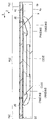
도 1은 일 실시 형태인 반도체 장치의 사시도이다.
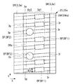
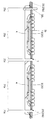
도 2는 도 1에 도시하는 반도체 장치의 하면도이다.
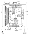
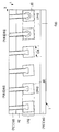
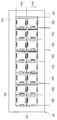
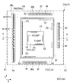
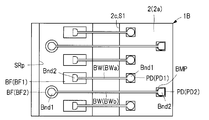
도 3은 도 1에 도시하는 밀봉체를 제거한 상태에서 배선 기판 상의 반도체 장치의 내부 구조를 나타내는 투시 평면도이다.
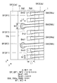
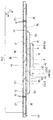
도 4는 도 1의 A-A선을 따른 단면도이다.
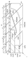
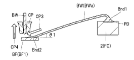
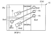
도 5는 도 3에 도시하는 복수의 와이어 중, 하단측의 반도체 칩과 배선 기판을 전기적으로 접속하는 와이어를 도시하는 확대 단면도이다.
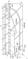
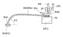
도 6은 도 3에 도시하는 복수의 와이어 중, 상단측의 반도체 칩과 배선 기판을 전기적으로 접속하는 와이어를 도시하는 확대 단면도이다.
도 7은 도 3에 도시하는 배선 기판의 칩 탑재면 측의 평면에 있어서, 본딩 핑거의 배치 밀도가 높은 영역을 확대하여 도시하는 확대 평면도이다.
도 8은 도 7에 나타내는 영역보다 본딩 핑거의 배치 밀도가 낮은 영역을 확대하여 도시하는 확대 평면도이다.
도 9는 일 실시 형태인 반도체 장치의 조립 플로우를 도시하는 설명도이다.
도 10은 도 9에 나타내는 기판 준비 공정에서 준비하는 배선 기판의 전체 구조를 도시하는 평면도이다.
도 11은 도 10에 도시하는 복수의 디바이스 형성부 중 1개에 있어서, 도 7에 나타내는 영역에 대응하는 부분의 확대 평면도이다.
도 12는 도 10에 도시하는 배선 기판 상에 반도체 칩을 탑재한 상태를 도시하는 확대 평면도이다.
도 13은 도 12의 A-A선을 따른 확대 단면도이다.
도 14는 도 12에 나타내는 반도체 칩과 배선 기판을, 와이어 본딩에 의해 전기적으로 접속한 상태를 도시하는 확대 평면도이다.
도 15는 도 13에 나타내는 반도체 칩과 배선 기판을, 와이어 본딩에 의해 전기적으로 접속한 상태를 도시하는 확대 단면도이다.
도 16은 정 본딩 방식의 제1 본드측에 있어서, 볼부를 패드에 접합한 상태를 도시하는 확대 단면도이다.
도 17은 정 본딩 방식의 제2 본드측에 있어서, 스티치부를 본딩 핑거에 접합한 상태를 도시하는 확대 단면도이다.
도 18은 역 본딩 방식의 제1 본드측에 있어서, 볼부를 본딩 핑거에 접합한 상태를 도시하는 확대 단면도이다.
도 19는 역 본딩 방식의 제2 본드측에 있어서, 스티치부를 범프 전극에 접합한 상태를 도시하는 확대 단면도이다.
도 20은 도 15에 도시하는 반도체 칩 및 복수의 와이어를 수지로 밀봉한 상태를 도시하는 확대 단면도이다.
도 21은 도 20에 나타내는 복수의 랜드 각각의 노출면에 땜납을 형성한 상태를 도시하는 확대 단면도이다.
도 22는 도 21에 나타내는 배선 기판을 다이싱 블레이드로 절단한 상태를 도시하는 확대 단면도이다.
도 23은 도 7에 대한 변형예를 도시하는 확대 평면도이다.
도 24는 도 3에 도시하는 반도체 장치에 대한 변형예에 있어서, 반도체 칩이 갖는 복수의 패드와 배선 기판의 복수의 본딩 핑거의 접속 관계를 모식적으로 도시하는 확대 평면도이다.
도 25는 도 24에 대한 변형예를 도시하는 확대 평면도이다.
도 26은 도 24에 대한 다른 변형예를 도시하는 확대 평면도이다.
도 27은 본딩 핑거의 형상이나 크기가 도 7에 나타내는 실시 형태와는 다른 실시 형태를 도시하는 확대 평면도이다.
도 28은 도 27의 A-A선을 따른 확대 단면도이다.
도 29는 본딩 핑거의 형상이나 크기가 도 7에 나타내는 실시 형태와는 다른 실시 형태를 도시하는 확대 평면도이다.
도 30은 본딩 핑거의 형상이나 크기가 도 7에 나타내는 실시 형태와는 다른 실시 형태를 도시하는 확대 평면도이다.
도 2는 도 1에 도시하는 반도체 장치의 하면도이다.
도 3은 도 1에 도시하는 밀봉체를 제거한 상태에서 배선 기판 상의 반도체 장치의 내부 구조를 나타내는 투시 평면도이다.
도 4는 도 1의 A-A선을 따른 단면도이다.
도 5는 도 3에 도시하는 복수의 와이어 중, 하단측의 반도체 칩과 배선 기판을 전기적으로 접속하는 와이어를 도시하는 확대 단면도이다.
도 6은 도 3에 도시하는 복수의 와이어 중, 상단측의 반도체 칩과 배선 기판을 전기적으로 접속하는 와이어를 도시하는 확대 단면도이다.
도 7은 도 3에 도시하는 배선 기판의 칩 탑재면 측의 평면에 있어서, 본딩 핑거의 배치 밀도가 높은 영역을 확대하여 도시하는 확대 평면도이다.
도 8은 도 7에 나타내는 영역보다 본딩 핑거의 배치 밀도가 낮은 영역을 확대하여 도시하는 확대 평면도이다.
도 9는 일 실시 형태인 반도체 장치의 조립 플로우를 도시하는 설명도이다.
도 10은 도 9에 나타내는 기판 준비 공정에서 준비하는 배선 기판의 전체 구조를 도시하는 평면도이다.
도 11은 도 10에 도시하는 복수의 디바이스 형성부 중 1개에 있어서, 도 7에 나타내는 영역에 대응하는 부분의 확대 평면도이다.
도 12는 도 10에 도시하는 배선 기판 상에 반도체 칩을 탑재한 상태를 도시하는 확대 평면도이다.
도 13은 도 12의 A-A선을 따른 확대 단면도이다.
도 14는 도 12에 나타내는 반도체 칩과 배선 기판을, 와이어 본딩에 의해 전기적으로 접속한 상태를 도시하는 확대 평면도이다.
도 15는 도 13에 나타내는 반도체 칩과 배선 기판을, 와이어 본딩에 의해 전기적으로 접속한 상태를 도시하는 확대 단면도이다.
도 16은 정 본딩 방식의 제1 본드측에 있어서, 볼부를 패드에 접합한 상태를 도시하는 확대 단면도이다.
도 17은 정 본딩 방식의 제2 본드측에 있어서, 스티치부를 본딩 핑거에 접합한 상태를 도시하는 확대 단면도이다.
도 18은 역 본딩 방식의 제1 본드측에 있어서, 볼부를 본딩 핑거에 접합한 상태를 도시하는 확대 단면도이다.
도 19는 역 본딩 방식의 제2 본드측에 있어서, 스티치부를 범프 전극에 접합한 상태를 도시하는 확대 단면도이다.
도 20은 도 15에 도시하는 반도체 칩 및 복수의 와이어를 수지로 밀봉한 상태를 도시하는 확대 단면도이다.
도 21은 도 20에 나타내는 복수의 랜드 각각의 노출면에 땜납을 형성한 상태를 도시하는 확대 단면도이다.
도 22는 도 21에 나타내는 배선 기판을 다이싱 블레이드로 절단한 상태를 도시하는 확대 단면도이다.
도 23은 도 7에 대한 변형예를 도시하는 확대 평면도이다.
도 24는 도 3에 도시하는 반도체 장치에 대한 변형예에 있어서, 반도체 칩이 갖는 복수의 패드와 배선 기판의 복수의 본딩 핑거의 접속 관계를 모식적으로 도시하는 확대 평면도이다.
도 25는 도 24에 대한 변형예를 도시하는 확대 평면도이다.
도 26은 도 24에 대한 다른 변형예를 도시하는 확대 평면도이다.
도 27은 본딩 핑거의 형상이나 크기가 도 7에 나타내는 실시 형태와는 다른 실시 형태를 도시하는 확대 평면도이다.
도 28은 도 27의 A-A선을 따른 확대 단면도이다.
도 29는 본딩 핑거의 형상이나 크기가 도 7에 나타내는 실시 형태와는 다른 실시 형태를 도시하는 확대 평면도이다.
도 30은 본딩 핑거의 형상이나 크기가 도 7에 나타내는 실시 형태와는 다른 실시 형태를 도시하는 확대 평면도이다.
(본원에 있어서의 기재 형식·기본적 용어·용법의 설명)
본원에 있어서, 실시 형태 기재는, 필요에 따라, 편의상 복수의 섹션 등으로 나누어서 기재하는데, 특히 그렇지 않은 취지를 명시했을 경우를 제외하고, 이들은 서로 독립 별개의 것이 아니고, 기재된 전후를 막론하고, 단일 예의 각 부분, 한쪽이 다른 쪽의 일부 상세 또는 일부 또는 전부의 변형예 등이다. 또한, 원칙으로서, 같은 부분은 반복 설명을 생략한다. 또한, 실시 형태에 있어서의 각 구성 요소는, 특히 그렇지 않은 취지를 명시했을 경우, 이론적으로 그 수에 한정되는 경우 및 문맥으로부터 명백하게 그렇지 않은 경우를 제외하고, 필수적인 것이 아니다.
마찬가지로 실시 형태 등의 기재에 있어서, 재료, 조성 등에 대해서, 「A를 포함하는 X」 등이라고 해도, 특히 그렇지 않은 취지를 명시했을 경우 및 문맥으로부터 명백하게 그렇지 않은 경우를 제외하고, A 이외의 요소를 포함하는 것을 배제하는 것이 아니다. 예를 들어, 성분에 대하여 말하면, 「A를 주요한 성분으로서 포함하는 X」 등의 의미이다. 예를 들어, 「실리콘 부재」 등이라고 해도, 순수한 실리콘에 한정되는 것이 아니라, SiGe(실리콘·게르마늄) 합금이나 기타 실리콘을 주요한 성분으로 하는 다원 합금, 기타의 첨가물 등을 포함하는 부재도 포함하는 것은 말할 필요도 없다. 또한, 금 도금, Cu층, 니켈·도금 등이라고 해도, 그렇지 않은 취지, 특히 명시했을 경우를 제외하고, 순수한 것뿐만 아니라, 각각 금, Cu, 니켈 등을 주요한 성분으로 하는 부재를 포함하는 것으로 한다.
또한, 특정한 수치, 수량으로 언급했을 때도, 특히 그렇지 않은 취지를 명시했을 경우, 이론적으로 그 수에 한정되는 경우 및 문맥으로부터 명백하게 그렇지 않은 경우를 제외하고, 그 특정한 수치를 초과하는 수치이어도 되고, 그 특정한 수치 미만의 수치이어도 된다.
또한, 실시 형태의 각 도면 중에 있어서, 동일 또는 같은 부분은 동일하거나 또는 유사한 기호 또는 참조 번호로 나타내고, 설명은 원칙으로서 반복하지 않는다.
또한, 첨부 도면에 있어서는, 도리어, 번잡해질 경우 또는 공극과의 구별이 명확할 경우에는, 단면이어도 해칭 등을 생략할 경우가 있다. 이것과 관련하여, 설명 등으로부터 명확할 경우 등에는, 평면적으로 폐쇄한 구멍이어도, 배경의 윤곽선을 생략할 경우가 있다. 또한, 단면이 아니어도, 공극이 아닌 것을 명시하기 위해서, 또는 영역의 경계를 명시하기 위해서, 해칭이나 도트 패턴을 표시하는 경우가 있다.
이하의 실시 형태에서 설명하는 기술은, 반도체 칩의 표면에 형성된 전극 패드와 반도체 칩이 탑재되는 배선 기판의 단자(본딩 핑거)를 금속선인 와이어를 통해 전기적으로 접속하는 반도체 장치에 널리 적용 가능하다. 본 실시 형태에서는, 일례로서, 배선 기판 상에 복수의 반도체 칩이 적층되어, 서로 전기적으로 접속된 SiP(System in Package)형의 반도체 장치를 다루어서 설명한다.
도 1은 본 실시 형태의 반도체 장치의 사시도, 도 2는, 도 1에 도시하는 반도체 장치의 하면도이다. 또한, 도 3은, 도 1에 도시하는 밀봉체를 제거한 상태에서 배선 기판 상의 반도체 장치의 내부 구조를 나타내는 투시 평면도이다. 또한, 도 4는 도 1의 A-A선을 따른 단면도이다. 도 4에서는, 정 본딩 방식의 와이어(BWa)와 역 본딩 방식의 와이어(BWb)의 루프 형상의 차이를 나타내기 위해서, 와이어(BWb)에 대해서, 이점 쇄선을 표시하여 나타내고 있다.
<반도체 장치>
먼저, 본 실시 형태의 반도체 장치(1)의 구성 개요에 대해서, 도 1 내지 도 4를 사용하여 설명한다. 본 실시 형태의 반도체 장치(1)는 복수의 반도체 칩(2)(도 3, 도 4 참조), 및 복수의 반도체 칩(2)이 탑재된 배선 기판(3)을 갖는다. 도 4에 도시한 바와 같이 복수의 반도체 칩(2)은 배선 기판(3)의 상면(칩 탑재면)(3a) 측에 겹쳐지게 탑재되어, 각각, 밀봉체(수지체)(4)에 의해 덮여 있다.
본 실시 형태에서는, 하단측에 탑재된 반도체 칩(2)은 예를 들어 아날로그 회로가 형성된 아날로그 칩(반도체 칩)(FC)이다. 또한, 아날로그 칩(FC) 상에 탑재된 반도체 칩(2)은 상기 아날로그 회로를 제어하는 제어 회로가 형성된 컨트롤러 칩(CC)이다. 이와 같이, 하나의 패키지 내에 복수의 반도체 칩(2)이 탑재된 반도체 패키지는, 멀티 칩형 반도체 장치라고 불린다. 또한, 하나의 패키지 내에 탑재된 복수의 반도체 칩(2)이 서로 전기적으로 접속되고, 시스템이 구성된 반도체 패키지는, SiP형 반도체 장치라고 불린다. SiP형 반도체 장치를 포함하는 멀티 칩형 반도체 장치는, 반도체 칩(2)마다 패키징을 행하는 경우와 비교하여, 실장 면적을 저감할 수 있다. 특히, 본 실시 형태와 같이 복수의 반도체 칩(2)을 적층한 경우에는, 복수의 반도체 칩(2)을 배열하여 배치하는 경우보다 더 실장 면적을 저감할 수 있다.
도 4에 도시한 바와 같이, 밀봉체(4)는 상면(4a), 상면(4a)과는 반대측에 위치하는 하면(4b), 및 상면(4a)과 하면(4b) 사이에 위치하는 측면(4c)을 갖고, 평면에서 보아 사각형을 이룬다. 도 1에 도시하는 예에서는, 밀봉체(4)의 평면적(상면(4a) 측으로부터 평면에서 보았을 때의 면적)은 배선 기판(3)의 평면적과 같으며, 밀봉체(4)의 측면(4c)은 배선 기판(3)의 측면(3c)과 이어지고 있다. 배선 기판(3) 및 밀봉체(4)의 평면 형상은, 예를 들어 1변의 길이가 예를 들어, 6mm 정도의 사각형을 이룬다. 또한, 반도체 장치(1)에 대한 박형화의 요구에 대응하기 위해서, 밀봉체(4)는 박형화되어 있다. 밀봉체(4)의 두께(높이), 즉, 도 4에 도시하는 상면(4a)으로부터 하면(4b)까지의 거리는, 예를 들어 600㎛ 내지 800㎛ 정도이다.
또한, 도 3 및 도 4에 도시한 바와 같이, 배선 기판(3)에 탑재되는 복수의 반도체 칩(2) 각각은, 표면(주면, 상면)(2a)과, 표면(2a)과는 반대측의 이면(주면, 하면)(2b)(도 4 참조)과, 이 표면(2a)과 이면(2b) 사이에 위치하는 측면(2c)(도 4 참조)을 갖고 있다. 또한, 반도체 장치(1)에 대한 박형화의 요구에 대응하기 위해서, 반도체 칩(2)은 박형화되어 있다. 또한, 반도체 칩(2) 각각의 두께(높이)는 예를 들어 200㎛ 내지 300㎛ 정도이다. 또한, 도 3에 도시한 바와 같이, 복수의 반도체 칩(2) 각각은, 평면에서 보아 사각형을 이룬다. 또한, 본 실시 형태에서는, 상단에 탑재되는 반도체 칩(2)(도 3에 도시하는 컨트롤러 칩(CC))의 평면 사이즈(평면적)는 하단측에 탑재되는 반도체 칩(2)(도 3에 도시하는 아날로그 칩(FC))의 평면 사이즈(평면적)보다 작다.
상세하게는, 도 3에 도시한 바와 같이, 복수의 반도체 칩(2) 각각은, 평면에서 보아, 변(S1), 변(S1)의 반대측 변(S2), 변(S1) 및 변(S2)와 교차하는 변(S3), 및 변(S3)의 반대측 변(S4)를 갖고 있다. 또한, 아날로그 칩(FC)의 변(S1)은, 컨트롤러 칩(CC)의 변(S1)을 따라 배치되고, 아날로그 칩(FC)의 변(S1)의 길이는, 컨트롤러 칩(CC)의 변(S1)의 길이보다 짧다. 또한, 아날로그 칩(FC)의 변(S2)은, 컨트롤러 칩(CC)의 변(S2)을 따라 배치되고, 아날로그 칩(FC)의 변(S2)의 길이는, 컨트롤러 칩(CC)의 변(S2)의 길이보다 짧다. 또한, 아날로그 칩(FC)의 변(S3)은, 컨트롤러 칩(CC)의 변(S3)을 따라 배치되고, 아날로그 칩(FC)의 변(S3)의 길이는, 컨트롤러 칩(CC)의 변(S3)의 길이보다 짧다. 또한, 아날로그 칩(FC)의 변(S4)은, 컨트롤러 칩(CC)의 변(S4)을 따라 배치되고, 아날로그 칩(FC)의 변(S4)의 길이는, 컨트롤러 칩(CC)의 변(S4)의 길이보다 짧다.
또한, 도 3에 도시하는 예에서는, 아날로그 칩(FC)의 각 변의 길이가, 컨트롤러 칩의 각 변보다 짧고, 평면에서 보아, 컨트롤러 칩(CC)의 전체가 아날로그 칩(FC)의 표면(2a)에 겹쳐 있다. 아날로그 칩(FC)은, 평면에서 보아, 예를 들어 1변의 길이가 3mm 내지 5mm 정도의 사각형을 이룬다. 또한, 컨트롤러 칩(CC)은, 평면에서 보아, 예를 들어 1변의 길이가 1mm 내지 2mm 정도의 사각형을 이룬다.
또한, 평면에서 보아 사각형을 이루는 반도체 칩(2)의 표면(2a)에는, 표면(2a)의 각 변을 따라, 각각 복수의 패드(PD)(단자, 전극, 전극 패드, 본딩 패드)가 배열되어 있다. 또한, 도시는 생략하지만, 반도체 칩(2)의 주면(상세하게는, 반도체 칩(2)의 기재(반도체 기판)의 주면(반도체 소자 형성면, 상면)에 설치된 반도체 소자 형성 영역)에는, 복수의 반도체 소자(회로 소자)가 형성된다. 그리고, 복수의 패드(PD)는, 반도체 칩(2)의 내부(상세하게는, 표면(2a)과 도시하지 않은 반도체 소자 형성 영역 사이)에 배치되는 배선층에 형성된 배선(도시는 생략)을 통해, 이 반도체 소자와 전기적으로 접속되어 있다.
반도체 칩(2)(상세하게는, 반도체 칩(2)의 기재인 반도체 기판)은 예를 들어 실리콘(Si)을 포함한다. 또한, 표면(2a)에는, 반도체 칩(2)의 기재 및 배선을 덮는 절연막이 형성되어 있고, 복수의 패드(PD) 각각의 표면은, 이 절연막에 형성된 개구부에 있어서, 절연막으로부터 노출되어 있다. 또한, 이 패드(PD)는 금속을 포함하고, 예를 들어, 주로 알루미늄(Al)을 포함한다. 또한, 예를 들어 이 패드(PD)에 다른 배선을 접속하여 다른 위치에 패드를 다시 배치하는, 소위 재배선 기술을 적용한 경우에는, 이 재배선의 일부가 새로운 패드가 된다. 이 경우에는, 구리(Cu)를 주성분으로 하는 배선의 표면에 니켈(Ni)을 형성하고, 또한, 이 니켈 위에 금(Au)을 형성한다.
또한, 아날로그 칩(FC) 및 컨트롤러 칩(CC)은, 배선 기판(3)의 상면(3a) 상에 탑재된다. 도 3에 도시하는 예에서는, 아날로그 칩(FC)은 배선 기판(3)의 상면(3a)의 중앙부에 탑재되고, 컨트롤러 칩(CC)은 아날로그 칩(FC)의 중앙부에 탑재되어 있다. 또한, 도 4에 도시한 바와 같이, 아날로그 칩(FC)은, 이면(2b)이 배선 기판(3)의 상면(3a)과 대향한 상태에서, 다이 본드재(접착재)(5)를 통해 배선 기판(3)에 탑재되어 있다. 즉, 복수의 패드(PD)가 형성된 표면(주면)(2a)의 반대면(이면(2b))을 칩 탑재면(상면(3a))과 대향시키는, 소위, 페이스 업 실장 방식에 의해 탑재되어 있다. 또한, 컨트롤러 칩(CC)은, 이면(2b)이 아날로그 칩(FC)의 표면(2a)과 대향한 상태에서, 다이 본드재(접착재)(6)를 통해 아날로그 칩(FC) 상에 탑재되어 있다.
다이 본드재(5)는 반도체 칩(2)과 배선 기판(3)을 접착 고정하는 페이스트 접착재이며, 예를 들어 페이스트 상태의 접착재를 경화시킴으로써, 반도체 칩(2)과 배선 기판(3)을 접착 고정하고 있다. 또한, 다이 본드재(6)는 반도체 칩(2)끼리를 접착 고정하는 필름 접착재이며, 예를 들어, DAF(Die Attach Film)라고 불리는 수지 필름 등을 경화시킴으로써, 상하단의 반도체 칩(2)을 접착 고정하고 있다. 단, 다이 본드재(5, 6)는, 상기에 한정되는 것은 아니고, 예를 들어, 다이 본드재(5)로서 상기한 수지 필름을 사용해도 되고, 다이 본드재(6)로서 페이스트 접착재를 사용해도 된다. 다이 본드재(5, 6)로서 사용되는 접착재는, 수지 필름의 경우도, 페이스트 접착재의 경우도, 에폭시 수지를 주성분으로 하는 것을 사용하는 경우가 많다.
또한, 도 4에 도시한 바와 같이, 배선 기판(3)은 반도체 칩(2)이 탑재된 상면(칩 탑재면)(3a), 상면(3a)과는 반대측의 하면(실장면)(3b), 및 상면(3a)과 하면(3b) 사이에 배치된 복수의 측면(3c)을 갖고 있다. 또한, 도 2 및 도 3에 도시한 바와 같이 평면에서 보아 사각형을 이룬다.
상세하게는, 도 3에 도시한 바와 같이, 배선 기판(3)은 평면에서 보아, 변(S1), 변(S1)의 반대측 변(S2), 변(S1) 및 변(S2)과 교차하는 변(S3), 및 변(S3)의 반대측 변(S4)을 갖고 있다. 또한, 도 3에 도시하는 예에서는, 반도체 칩(2)의 변(S1, S2, S3, S4) 각각이, 배선 기판(3)의 변(S1, S2, S3, S4)을 따라 탑재되어 있다. 또한, 상기한 바와 같이, 도 1에 도시하는 예에서는, 배선 기판(3)의 평면적은 밀봉체(4)의 평면적과 같으며, 배선 기판(3)의 평면 형상은, 예를 들어 1변의 길이가 예를 들어, 6mm 정도의 사각형을 이룬다. 도 1에 도시하는 예에서는 직사각형이다. 또한, 배선 기판(3)의 두께(높이), 즉, 도 4에 도시하는 상면(3a)으로부터 하면(3b)까지의 거리는, 예를 들어 0.2mm 내지 0.4mm 정도이다.
또한, 배선 기판(3)은 복수의 배선층(도 4에 도시하는 예에서는 상면 배선층 및 하면 배선층의 2층)을 갖는다. 각 배선층 간에 배치되는 절연층(3e)은 예를 들어, 유리 섬유 또는 탄소 섬유에 수지를 함침시킨 프리프레그에 의해 구성되어 있다. 또한, 절연층(3e)의 상면측에는 복수의 본딩 핑거(BF)가, 절연층(3e)의 하면측에는 복수의 랜드(LD)가, 각각 형성되고, 복수의 배선(3r)을 통해 본딩 핑거(BF)와 랜드(LD)가 전기적으로 접속되어 있다.
또한, 도 3에 도시한 바와 같이, 배선 기판(3)의 상면(3a)에는, 배선 기판(3)과 반도체 칩(2)을 전기적으로 접속하기 위한 내부 인터페이스용 단자인 복수의 본딩 핑거(단자, 칩 탑재면측 단자, 본딩 리드)(BF)가 형성된다. 복수의 본딩 핑거(BF)는, 반도체 칩(2)이 탑재되는 칩 탑재 영역의 주위에, 반도체 칩(2)의 각 변을 따라 배치되어 있다. 상세하게는, 배선 기판(3)의 상면(3a)에는, 절연층(3e)의 상면측에 형성된 배선을 덮는 솔더 레지스트막(절연막)(SR)이 형성되고, 솔더 레지스트막(SR)에 형성된 개구부(SRp)에 있어서, 복수의 본딩 핑거(BF)가, 솔더 레지스트막(SR)으로부터 노출되어 있다.
또한, 반도체 칩(2)의 복수의 패드(PD)와, 배선 기판(3)의 복수의 본딩 핑거(BF)는, 복수의 와이어(도전성 부재)(BW)를 통해 각각 전기적으로 접속된다. 또한, 본 실시 형태에 있어서의 복수의 와이어(BW)는, 예를 들어, 금(Au)을 포함하지만, 이외의 재료로서, 예를 들어 구리(Cu)를 주로 하는 금속을 포함하는 와이어를 사용해도 된다. 본딩 핑거(BF) 및 와이어(BW)의 상세에 대해서는, 후술한다.
또한, 도 2에 도시한 바와 같이, 배선 기판(3)의 하면(3b)에는, 복수의 랜드(외부 단자, 전극 패드, 외부 전극 패드)(LD)가 형성된다. 복수의 랜드(LD)는, 행렬 형상(매트릭스 형상)으로 배치되어 있다. 또한, 도 4에 도시한 바와 같이 복수의 랜드(LD)는, 배선 기판(3)에 형성된 복수의 배선(3r)을 통해 복수의 본딩 핑거(BF)와 전기적으로 접속된다. 즉, 복수의 랜드(LD) 각각은 복수의 반도체 칩(2) 각각과 전기적으로 접속되고, 복수의 반도체 칩(2)과 도시하지 않은 외부 기기를 전기적으로 접속하는 외부 인터페이스용의 단자이다.
이렇게 외부 단자를 배선 기판의 실장면측에 행렬 형상으로 배치하는 반도체 장치를 에리어 어레이형의 반도체 장치라고 칭한다. 에리어 어레이형의 반도체 장치는, 배선 기판(3)의 실장면(하면(3b)) 측을, 외부 단자의 배치 스페이스로서 유효하게 활용할 수 있으므로, 외부 단자의 수가 증대해도 반도체 장치의 실장 면적의 증대를 억제할 수 있는 점에서 바람직하다. 즉, 고기능화, 고집적화에 수반하여, 외부 단자수가 증대한 반도체 장치를 공간 절약하여 실장할 수 있다.
또한, 도 2에서는, 외부 단자의 수가 140개인 예를 나타내고 있지만, 단자수나 레이아웃에 대해서는 이것에 한정되지 않는다. 또한, 도 4에서는, 절연층(3e)의 상면과 하면에 각각 배선층을 형성한 배선 기판(3)을 예시적으로 나타내고 있지만, 배선층의 수는 이것에 한정되지 않고, 2층보다 많은 배선층 구조로 할 수도 있다.
도 4에 도시하는 배선 기판(3)의 도전로를 구성하는 본딩 핑거(BF), 랜드(LD) 및 배선(3r)은 금속막을 패터닝함으로써 형성되고, 예를 들어 구리(Cu)를 주체로 하는 도전막으로 구성한다. 또한, 배선(3r) 중, 절연층(3e)의 상면측과 하면측을 도통시키는 배선(3r)은 예를 들어 관통 구멍에 금속막을 매립함으로써 형성되고, 예를 들어 구리(Cu)를 주체로 하는 도전막으로 구성한다. 여기서, 구리를 주체로 하는 도전막에는, 구리 단체, 구리 합금, 또는, 구리 막 상에 다른 금속막(예를 들어 니켈막 등)을 적층한 금속막이 포함되고, 배선 기판(3)에 요구되는 사양에 따라서 이들을 선택할 수 있다.
또한, 복수의 랜드(LD)는, 배선 기판(3)의 하면(3b)을 덮는 솔더 레지스트막(절연막)(3h)으로부터 각각 노출되어 있다. 상세하게는, 배선 기판(3)의 하면(3b)에는, 절연층(코어 절연층)(3e)의 하면측에 형성된 배선을 가리는 솔더 레지스트막(절연막)(3h)이 형성되고, 솔더 레지스트막(3h)에 형성된 복수의 개구부에 있어서, 랜드(LD) 각각이, 솔더 레지스트막(3h)으로부터 노출되어 있다.
또한, 본 실시 형태에서는, 랜드(LD) 각각의 노출면이 땜납재(7)로 덮여 있다. 반도체 장치(1)를 도시하지 않은 실장 기판에 실장할 때에는, 실장 기판측의 단자와 반도체 장치(1)를 전기적으로 접속하는 도전성 접합재로서는, 땜납을 사용하는 경우가 많다. 따라서, 외부 단자인 랜드(LD)의 솔더 레지스트막(3h)으로부터의 노출면에, 땜납재(7)를 형성함으로써, 반도체 장치(1)를 도시하지 않은 실장 기판에 실장할 때에 땜납의 습윤성을 향상시킬 수 있다. 도 1, 도 2 및 도 4에 도시한 바와 같이, 땜납재(7)를 볼 형상으로 형성한 경우, BGA(Ball Grid Array)형이라고 불린다. 또한, 도시는 생략하지만, 땜납재(7)를 형성하지 않고, 랜드(LD)를 노출시킨 구조, 또는 랜드(LD)의 노출면에 얇게 땜납재, 또는 땜납재 이외의 금속재료를 포함하는 도금막을 형성한 변형예의 반도체 장치는, LGA(Land Grid Array)형이라고 불린다.
땜납재(7)는 납(Pb)을 실질적으로 포함하지 않는, 소위, 납 프리 땜납을 포함하고, 예를 들어 주석(Sn)만, 주석-비스무트(Sn-Bi), 또는 주석-은-구리(Sn-Ag-Cu) 등이다. 여기서, 납 프리 땜납이란, 납(Pb)의 함유량이 0.1wt% 이하의 것을 의미하고, 이 함유량은, RoHs(Restriction of Hazardous Substances) 지령의 기준으로서 정해져 있다. 이하, 본원에 있어서, 땜납에 대하여 설명할 경우에는, 특히 그렇지 않은 취지를 명시했을 경우를 제외하고, 납 프리 땜납을 가리킨다.
< 와이어 및 본딩 핑거의 상세>
이어서, 도 3 및 도 4에 도시하는 와이어(BW)에 의한 전기적 접속 부분의 상세 구조에 대하여 설명한다. 도 5는, 도 3에 도시하는 복수의 와이어 중, 하단측의 반도체 칩과 배선 기판을 전기적으로 접속하는 와이어를 도시하는 확대 단면도이다. 또한, 도 6은, 도 3에 도시하는 복수의 와이어 중, 상단측의 반도체 칩과 배선 기판을 전기적으로 접속하는 와이어를 도시하는 확대 단면도이다. 또한, 도 7은, 도 3에 도시하는 배선 기판의 칩 탑재면측의 평면에 있어서, 본딩 핑거의 배치 밀도가 높은 영역을 확대하여 도시하는 확대 평면도이다. 또한, 도 8은, 도 7에 나타내는 영역보다 본딩 핑거의 배치 밀도가 낮은 영역을 확대하여 도시하는 확대 평면도이다. 또한, 도 27, 도 29, 도 30 각각은, 본딩 핑거의 형상이나 크기가 도 7에 나타내는 실시 형태와는 다른 실시 형태를 도시하는 확대 평면도이다. 또한, 도 28은 도 27의 A-A선에 따른 확대 단면도이다.
또한, 도 5 및 도 6에서는, 정 본딩 방식의 와이어(BWa)와 역 본딩 방식의 와이어(BWb)의 루프 형상의 차이를 나타내기 위해서, 도 5에서는 와이어(BWb)에 대해서, 도 6에서는 와이어(BWa)에 대해서, 각각 이점 쇄선을 표시하여 나타내고 있다. 또한, 도 7은 도 3에 도시하는 반도체 칩(2)이 갖는 4변 중, 변(S1)에 따른 본딩 핑거군의 일부를 확대한 평면도, 도 8은, 변(S3)에 따른 본딩 핑거군의 일부를 확대한 평면도이다. 또한, 도 7 및 도 8에 나타내는 본딩 핑거(BF)에는, 금속 패턴을 전기 도금법에 의해 형성하기 위한 급전선이 형성되어 있으나, 도 7 및 도 8에서는, 보기 쉽도록, 급전선의 도시를 생략하고 있다. 또한, 도 7 및 도 8에서는, 도 4에 도시하는 배선(3r)이 와이어(BW)와 겹치는 위치에 형성되어 있으나, 보기 쉽도록, 배선(3r)의 부호는 도시를 생략하고 있다. 배선(3r) 및 급전선의 레이아웃 예는, 후술하는 도 11에 있어서 나타낸다.
도 3에 도시한 바와 같이, 본 실시 형태에서는, 복수의 패드(PD)와 복수의 본딩 핑거(BF)는, 복수의 와이어(BW)를 통해 각각 전기적으로 접속되어 있다. 와이어(BW)는, 한쪽의 단부가 패드(PD)에, 다른 쪽의 단부가 본딩 핑거(BF)에 접속된 금속 세선이다. 반도체 칩(2)과 배선 기판(3)을 전기적으로 접속할 때의 와이어 본딩 방법은, 접속 순서의 차이에 의해 이하의 2종류로 분류할 수 있다.
먼저, 제1 본드측(먼저 접속하는 단자)이 반도체 칩(2)의 패드(PD)이며, 제2 본드측(나중에 접속하는 단자)이 배선 기판(3)의 본딩 핑거(BF)인, 소위, 정 본딩 방식이 있다. 또한, 제1 본드측이 배선 기판(3)의 본딩 핑거(BF)이며, 제2 본드측이 반도체 칩(2)의 패드(PD)인, 소위, 역 본딩 방식이 있다.
정 본딩 방식의 경우, 도 5에 도시하는 와이어(BWa)와 같이, 제1 본드측인 반도체 칩(2)의 패드(PD)에는, 예를 들어 볼 본딩 방식에 의해, 와이어(BW)의 한쪽 단부가 접속된다. 볼 본딩 방식에서는, 와이어의 선단에 형성된 구형의 금속 덩어리인 볼부(Bnd1)를 패드(PD)에 접촉시켜서, 도시하지 않은 모세관으로 가압함으로써 패드(PD)와 볼부(Bnd1)가 열압착된다. 이때, 모세관으로부터 초음파를 인가하고, 패드(PD)와 볼부(Bnd1)의 접합성을 향상시키는 경우도 있다.
또한, 볼부(Bnd1)와는 반대측의 단부는, 제2 본드측인 배선 기판(3)의 본딩 핑거(BF)에, 예를 들어, 스티치 본딩 방식에 의해 접속된다. 스티치 본딩 방식에서는, 와이어(BW)의 일부를 제2 본드측인 본딩 핑거(BF)에 접촉시킨 후, 도시하지 않은 모세관으로 와이어(BW)를 본딩 핑거(BF)에 가압하면서, 본딩 핑거(BF)의 연장 방향을 따라서 이동시킨다. 이 모세관의 동작에 의해, 와이어(BW)의 제2 본드측의 단부에서는 와이어(BW)가 찌부러져서 소성 변형하여, 스티치부(Bnd2)가 형성된다.
한편, 역 본딩 방식의 경우, 도 6에 나타내는 와이어(BWb)와 같이 배선 기판(3)의 본딩 핑거(BF)가 제1 본드측이 되므로, 와이어(BW)의 한쪽 단부는, 볼 본딩 방식에 의해 배선 기판(3)의 본딩 핑거(BF)에 접속된다. 바꿔 말하면, 본딩 핑거(BF)에 볼부(Bnd1)가 접속된다. 또한, 제2 본드측이 되는 반도체 칩(2)의 패드(PD)와의 접속 부분에는, 스티치 본딩 방식에 의해 와이어(BW)의 다른 쪽 단부가 접속된다.
상기한 바와 같이 볼부(Bnd1)는 구형의 금속 덩어리를 피접속부에 가압하여 형성하므로, 도 7에 도시한 바와 같이, 평면 형상이 원형(타원형도 포함됨)이 된다. 한편, 스티치부(Bnd2)는, 와이어(BW)를 본딩 핑거(BF)에 가압하면서, 본딩 핑거(BF)의 연장 방향을 따라서 모세관을 이동시켜서 형성하므로, 도 7에 도시한 바와 같이, 평면 형상은, 반타원형(반원형도 포함됨)이 된다.
여기서, 도 3에 도시하는 반도체 칩(2)의 패드(PD)에 스티치 본딩 방식으로 와이어(BW)를 접속하는 경우, 패드(PD)에 직접 와이어(BW)를 접속할 수도 있다. 이 경우, 도 6에 나타내는 스티치부(Bnd2)와 패드(PD)를 접합한다. 단, 스티치 본딩 방식의 경우, 상기한 바와 같이, 와이어(BW)의 일부를 접속 대상물에 가압하면서, 도시하지 않은 모세관을 평면 방향으로 이동시킴으로써 접속 강도를 향상시킬 수 있다. 따라서, 모세관 동작에 의해 반도체 칩(2) 패드(PD) 주변에 인가되는 응력을 저감하는 관점에서는, 도 6에 도시한 바와 같이 패드(PD)와 스티치부(Bnd2) 사이에 범프 전극(BMP)을 개재시키는 것이 바람직하다. 범프 전극(BMP)은, 패드(PD) 위에 돌출되도록 형성된 돌기 전극이며, 예를 들어 금(Au)을 포함한다. 금을 포함하는 범프 전극(BMP)은, 상기한 볼 본딩 방식을 응용하여 형성할 수 있다. 즉, 와이어의 단부에 형성된 볼 형상의 부분(볼부)을 패드(PD)에 접합한 후, 접합 부분의 근방에서 와이어를 절단한다. 이에 의해, 범프 전극(BMP)을 형성할 수 있다.
또한, 본 실시 형태에서는, 도 3에 도시하는 복수의 와이어(BW)에는, 정 본딩 방식에 의해 형성되는 와이어(BWa)와, 역 본딩 방식에 의해 형성되는 와이어(BWb)가 포함된다. 정 본딩 방식과 역 본딩 방식을 혼재시키는 이유로서는, 여러가지 이유가 있지만, 본 실시 형태에서는, 하단측의 아날로그 칩(FC)에는 정 본딩 방식의 와이어(BWa)가 접속되고, 상단측의 컨트롤러 칩(CC)에는 역 본딩 방식의 와이어(BWb)가 접속되어 있다.
도 6에 도시한 바와 같이, 역 본딩 방식에 의해 형성되는 와이어(BWb)는, 제2 본드측의 위치가 제1 본드측의 위치보다 높은 위치(상대적으로 밀봉체(4)의 상면(4a)에 가까운 위치)에 배치된다. 따라서, 상단측에 배치되는 반도체 칩(2)에 접속되는 와이어(BW)를, 모두 역 본딩 방식에 의해 형성함으로써, 와이어(BWb)의 와이어 높이를 저감하고, 밀봉체(4)의 두께를 얇게 할 수 있다. 한편, 하단측의 반도체 칩(2)의 패드(PD)는, 상단측의 반도체 칩(2)의 패드보다 낮은 위치에 배치되어 있기 때문에, 도 5에 도시한 바와 같이 정 본딩 방식으로 형성해도, 와이어(BWa)의 와이어 루프의 최고 지점은, 와이어(BWb)의 와이어 루프의 최고 지점보다 낮은 위치에 배치된다. 따라서, 하단측의 반도체 칩(2)에 접속되는 와이어(BW)를, 정 본딩 방식에 의해 형성함으로써, 범프 전극(BMP)(도 6 참조) 등을 형성할 필요가 없어, 제조 효율을 향상시킬 수 있다.
또한, 도 3에 도시한 바와 같이, 본 실시 형태의 반도체 장치(1)는 평면에서 보아 반도체 칩(2)의 각 변을 따라 각각 복수의 본딩 핑거(BF)가 배치되어 있다. 각 변을 따라 배치되는 본딩 핑거(BF)의 수는, 다양한 변형예를 적용할 수 있지만, 도 3에 도시하는 예에서는, 반도체 칩(2)의 변(S1)을 따라 배치되는 본딩 핑거(BF)의 수가, 다른 변(S2, S3, S4)을 따라 배치되는 본딩 핑거(BF)의 수보다 많다. 본딩 핑거(BF)는, 상기한 바와 같이 반도체 장치(1)의 내부 인터페이스용의 단자이므로, 반도체 칩(2)이 구비하는 회로의 레이아웃에 따라, 반도체 칩(2)의 각 변을 따라 배치되는 본딩 핑거(BF)의 수가 상이한 경우가 있다.
본 실시 형태의 예에서는, 하단측에 배치되는 아날로그 칩(FC)이 구비하는 복수의 패드(PD) 중, 변(S1) 측에는 아날로그 회로에 대하여 스위칭 신호를 입출력하는 패드(PD)가 집약 배치되어 있다. 이렇게 신호 입출력용의 패드(PD)를 반도체 칩(2)에 1변을 따라서 집약 배치함으로써, 예를 들어, 신호 전송 거리의 등장화가 도모하기 쉬워진다. 또한, 상단측에 배치되는 컨트롤러 칩(CC)이 구비하는 복수의 패드(PD) 중, 아날로그 칩(FC) 사이에서 신호의 입출력을 행하는 패드(PD)는, 아날로그 칩(FC)과 컨트롤러 칩(CC)의 전송 거리가 짧아지도록 배열하는 것이 바람직하다. 이 결과, 컨트롤러 칩(CC)이 구비하는 복수의 패드(PD) 중 일부는, 컨트롤러 칩(CC)의 변(S1)을 따라 배치된다. 그리고, 컨트롤러 칩(CC)의 변(S1)을 따라 배치되어 있는 패드(PD)에 접속되는 와이어(BWb)는, 아날로그 칩(FC)의 변(S1)을 따라 배치되어 있는 본딩 핑거(BF)에 접속된다. 또한, 컨트롤러 칩(CC)에 범용성을 갖게 할 경우, 컨트롤러 칩(CC)의 복수의 패드(PD)는, 컨트롤러 칩(CC)의 각 변을 따라 배치하게 된다. 따라서, 컨트롤러 칩(CC)에 접속되는 복수의 와이어(BW) 중 일부는, 배선 기판(3)의 복수의 본딩 핑거(BF) 중, 반도체 칩(2)의 변(S1)을 따라 배치되는 본딩 핑거(BF)에 접속되게 된다.
상기와 같이, 본 실시 형태에서는, 반도체 칩(2)의 각 변 중 변(S1)을 따라 배치되는 복수의 본딩 핑거(BF)는, 다른 변(S2, S3, S4)을 따라 배치되는 본딩 핑거(BF)보다 수가 많다. 또한, 반도체 칩(2)의 변(S1)을 따라 배치되는 본딩 핑거(BF)에 접속되는 복수의 와이어(BW)는, 정 본딩 방식의 와이어(BWa)와 역 본딩 방식의 와이어(BWb)가 혼재한 상태가 된다.
여기서, 본딩 핑거(BF)의 수가 많아지면, 반도체 장치(1) 전체의 평면 사이즈의 증대를 억제하기 위해서는, 여기의 본딩 핑거(BF)의 폭 및 배치 간격을 작게 하게 된다. 예를 들어, 도 3에 도시하는 복수의 본딩 핑거군 중, 반도체 칩(2)의 변(S1)을 따라 배치되는 본딩 핑거군을 구성하는 본딩 핑거(BF)의 폭은, 변(S2, S3, S4)을 따라 배치되는 본딩 핑거군을 구성하는 본딩 핑거(BF)의 폭보다 좁다.
볼 본딩 방식에 의해 본딩 핑거(BF)와 와이어(BW)를 접속하는 경우, 와이어 루프 형상을 안정화시키는 관점, 또는, 와이어(BW)와 본딩 핑거(BF)와의 접합 강도를 향상시키는 관점에서, 볼부(Bnd1)(도 6 참조)와 본딩 핑거(BF)와의 밀착 면적을 크게 하는 것이 바람직하다. 예를 들어, 도 27에 도시한 바와 같이, 평면에서 보아, 볼부(Bnd1)의 일부가, 본딩 핑거(BF)로부터 밀려나와 있는 상태보다, 도 7에 도시한 바와 같이 볼부(Bnd1)의 전체가 본딩 핑거(BF)와 겹쳐있는 쪽이, 볼부(Bnd1)와 본딩 핑거(BF)와의 밀착 면적을 크게 할 수 있다.
상세하게는, 도 28에 도시한 바와 같이, 본딩 핑거(BF)는, 연장 방향과 직교하는 방향으로 절단했을 때의 단면 형상이 사다리꼴이 되어 있다. 즉, 본딩 핑거(BF)의 와이어(BW)와의 접합면인 상면의 폭(Wtp)은, 하면(배선 기판(3)의 상면(3a)에 밀착하는 면)의 폭(Wbt)보다 작다. 예를 들어, 설계 치수를 55㎛로 한 경우, 하면의 폭(Wbt)이 55㎛가 되도록 형성하면, 상면의 폭(Wtp)은, 40㎛ 정도가 된다. 이로 인해, 예를 들어, 볼부(Bnd1)의 폭이 본딩 핑거(BF)의 설계 치수와 동일 정도의 경우, 볼부(Bnd1)와 본딩 핑거(BF)의 접합면에서는, 볼부(Bnd1)의 일부가 밀려나오게 된다. 여기서, 볼부(Bnd1)의 폭이란, 평면에서 보아, 와이어(BWb)(도 7 참조)의 연장 방향에 대하여 직교하는 방향에 있어서의 볼부(Bnd1)의 길이이다. 볼부(Bnd1)의 평면 형상을 원형으로 간주했을 경우, 볼부(Bnd1)의 폭은, 볼부(Bnd1)의 지름(직경)으로 바꿔 말할 수도 있다.
한편, 스티치 본딩 방식에 의해 본딩 핑거(BF)와 와이어(BW)를 접속하는 경우, 상기한 바와 같이, 와이어(BW)의 일부를 찌부러뜨려서, 본딩 핑거(BF)의 연장 방향을 따라서 모세관을 이동시킴으로써 접합한다. 따라서, 본딩 핑거(BF)의 연장 거리를 확보할 수 있으면, 본딩 핑거(BF)의 폭은 좁아도 된다. 또한, 도 28에 도시한 바와 같이, 스티치부(Bnd2)의 폭이 볼부(Bnd1)의 폭보다 작은 경우, 스티치부(Bnd2)는 본딩 핑거(BF)로부터, 밀려나오기 어려워진다. 여기서, 스티치부(Bnd2)의 폭이란, 평면에서 보아, 와이어(BWa)(도 7 참조)의 연장 방향에 대하여 직교하는 방향에 있어서의 스티치부(Bnd2)의 최대의 길이이다. 스티치부(Bnd2)의 평면 형상을 반원형으로 간주했을 경우, 스티치부(Bnd2)의 폭은, 스티치부(Bnd2)의 지름(직경)으로 바꿔 말할 수도 있다.
본원 발명자는, 도 29에 도시한 바와 같이, 볼부(Bnd1)를 접속하는 본딩 핑거(BF2)의 폭(W2)을, 스티치부(Bnd2)를 접속하는 본딩 핑거(BF1)의 폭(W1)보다 넓게 하고, 일렬로 배열하는 실시 형태에 대하여 검토하였다. 도 29에 나타내는 실시 형태의 경우, 볼부(Bnd1)와 본딩 핑거(BF)의 밀착 면적이, 도 27에 나타내는 실시 형태보다 커진다. 또한, 볼부(Bnd1)를 접속하는 본딩 핑거(BF2)의 폭을 선택적으로 크게 하고 있으므로, 모든 본딩 핑거(BF)의 폭을 크게 하는 실시 형태와 비교하면, 패키지의 평면 사이즈의 증대를 억제할 수 있다. 그러나, 도 29에 나타내는 실시 형태의 경우, 도 27에 나타내는 실시 형태와 비교하면, 본딩 핑거군의 길이(도 29에 나타내는 Y 방향의 길이)가 커지므로, 패키지의 평면 사이즈가 커져버린다.
따라서, 이어서, 도 30에 도시한 바와 같이, 복수의 본딩 핑거(BF)를 복수 열로, 소위, 지그재그 형상으로 배치하는 실시 형태에 대하여 검토하였다. 도 30에 나타내는 실시 형태의 경우, 본딩 핑거(BF) 각각의 폭을 굵게 할 수 있으므로, 볼부(Bnd1)와 본딩 핑거(BF)의 밀착 면적이, 도 27에 나타내는 실시 형태보다 커진다. 또한, 본딩 핑거(BF)를 복수 열로 배치함으로써, 본딩 핑거군의 길이를 작게 할 수 있으므로, 패키지의 평면 사이즈의 증대를 억제할 수 있다.
그러나, 도 30에 도시한 바와 같이, 제1번째 열의 배치 열(Bd1)과, 제2번째 열의 배치 열(Bd2)에, 각각 스티치 본딩 방식으로 와이어(BWa)를 접속하는 경우, 제2번째 열의 배치 열(Bd2)이 접속되는 와이어(BWa)의 일부가, 제1번째 열에 배치되는 본딩 핑거(BF)의 일부에 접촉해버릴 우려가 있다. 그리고, 복수 열로 배치되는 본딩 핑거(BF)의 이격 거리를 가깝게 할수록, 와이어(BWa)와 본딩 핑거(BF)가 접촉하기 쉬워진다. 바꿔 말하면, 와이어(BWa)와 본딩 핑거(BF)의 접촉을 억제하기 위해서, 제1번째 열의 배치 열(Bd1)과 제2번째 열의 배치 열(Bd2)의 이격 거리를 크게 할 필요가 있다. 이 결과, 도 30에 나타내는 실시 형태의 경우에도, 패키지의 평면 사이즈가 커져버린다.
본원 발명자는, 상기의 검토 결과를 근거로 하여, 도 7에 나타내는 실시 형태를 발견하였다. 본 실시 형태에서는, 도 7에 도시한 바와 같이, 다수의 본딩 핑거(BF)가 배치되는 본딩 핑거군에 있어서는, 본딩 핑거(BF)가 복수 열에 걸쳐서 형성되어 있다. 먼저, 도 3에 도시하는 반도체 칩(2)의 변(S1)에 상대적으로 가까운 쪽의 제1번째 열 배치 열(Bd1)에는, 스티치 본딩용의 본딩 핑거(BF1)가 형성되어 있다. 또한, 도 3에 도시하는 반도체 칩(2)의 변(S1)으로부터의 거리가 제1번째 열보다 먼, 제2번째 열의 배치 열(Bd2)에는, 볼 본딩용의 본딩 핑거(BF2)가 형성되어 있다. 또한, 제2번째 열에는 스티치 본딩용의 본딩 핑거(BF1)는 형성되어 있지 않다. 바꿔 말하면, 본 실시 형태에서는, 상대적으로 반도체 칩(2)(도 3 참조)에 가까운 제1번째 열에, 정 본딩 방식용의 본딩 핑거(BF1)를 배치하고, 반도체 칩(2)으로부터의 거리가 제1번째 열보다 먼 제2번째 열에, 역 본딩 방식용의 본딩 핑거(BF2)를 배치하고 있다.
또한, 상대적으로 본딩 핑거(BF)의 배치 밀도가 높은 본딩 핑거군에 있어서, 정 본딩 방식으로 와이어(BWa)가 접속되는 제1번째 열의 본딩 핑거(BF1)는, 평면에서 보아 직사각형을 이루고, 본딩 핑거(BF1)의 연장 방향의 길이(L1)는, 연장 방향과 직교하는 방향의 길이(폭(W1))보다 길다. 도 3에 도시하는 예에서는, 반도체 칩(2)의 외측 테두리를 구성하는 4변 중, 변(S2, S3, S4)을 따라 배치되는 본딩 핑거군에서는, 변(S1)을 따라 배치되는 본딩 핑거군보다, 본딩 핑거(BF)의 배치 밀도가 낮다. 이로 인해, 도 7과 도 8을 비교하여 알 수 있는 바와 같이, 도 7에 나타내는 제1번째 열의 본딩 핑거(BF1)의(연장 방향과 직교하는 방향의 길이) 폭(W1)은, 도 8에 나타내는 다른 본딩 핑거군의 본딩 핑거(BF)의 폭(W3)보다 작아지고 있다.
이와 같이, 상대적으로 본딩 핑거(BF)의 배치 밀도가 높은 영역에 형성되는 본딩 핑거(BF1)의 폭(W1)을 작게 함으로써, 도 7에 나타내는 배치 열(Bd1)에 다수의 본딩 핑거(BF1)를 배치해도, 패키지의 평면 사이즈의 증대(도 7에 나타내는 예에서는 Y 방향의 길이 증대)를 억제할 수 있다.
또한, 본 실시 형태에서는, 하나의 개구부(SRp) 내에 본딩 핑거(BF1) 및 본딩 핑거(BF2)를 포함하는 복수의 본딩 핑거(BF)가 배치되어 있다. 예를 들어, 도 3에 도시하는 예에서는, 복수의 본딩 핑거(BF)에 의해 구성되는 본딩군마다 하나의 개구부(SRp)가 형성되어 있다. 바꿔 말하면, 하나의 본딩 핑거군에서는, 인접하는 본딩 핑거(BF) 사이에 솔더 레지스트막(SR)이 배치되어 있지 않다. 이와 같이, 하나의 개구부(SRp) 내에 복수의 본딩 핑거(BF)가 배치되도록 구성함으로써, 인접하는 본딩 핑거(BF) 간의 간격을 짧게 할 수 있다. 이 결과, 도 7에 나타내는 배치 열(Bd1)에 다수의 본딩 핑거(BF1)를 배치해도, 패키지의 평면 사이즈의 증대(도 7에 나타내는 예에서는 Y 방향의 길이 증대)를 억제할 수 있다. 단, 본딩 핑거(BF)의 배치 스페이스에 여유가 있는 영역에서는, 하나의 본딩 핑거군에 복수의 개구부(SRp)를 설치해도 된다. 예를 들어, 도 3에 도시하는 예에서는, 반도체 칩(2)의 변(S2), 변(S3), 또는 변(S4)을 따라 배치되어 있는 본딩 핑거군에서는, 복수의 개구부(SRp)를 설치할 수 있다.
또한, 제1번째 열의 본딩 핑거(BF1)와 제2번째 열의 본딩 핑거(BF2)의 폭 방향의 비교를 하면, 제1번째 열의 본딩 핑거(BF1)의 폭(W1)은, 제2번째 열의 본딩 핑거(BF2)의 폭(W2)(도 7에서는, Y 방향에 있어서의 길이)보다 작다. 바꿔 말하면, 본딩 핑거(BF2)의 폭(W2)은, 본딩 핑거(BF1)의 폭(W1)보다 크다. 예를 들어, 도 7에 나타내는 예에서는, 본딩 핑거(BF1)의 폭(W1)은 설계 치수가 55㎛ 정도인 것에 대해, 본딩 핑거(BF2)의 폭(W2)은, 설계 치수가 80㎛ 정도이다. 도 28을 사용하여 설명한 예에 꼭 들어맞춰서 설명하면 본딩 핑거(BF1)(도 7 참조)의 상면의 폭(Wtp)은 40㎛ 정도인데, 본딩 핑거(BF2)(도 7 참조)의 상면의 폭(Wtp)은 60㎛ 정도이다.
이로 인해, 예를 들어 도 7에 도시한 바와 같이, 와이어(BWb)의 볼부(Bnd1)의 폭(직경)이 와이어(BWa)의 스티치부(Bnd2)의 폭(와이어(BW)의 연장 방향에 대하여 직교하는 방향의 길이)보다 큰(굵은) 경우에도, 볼부(Bnd1)의 하면 전체를 본딩 핑거(BF2)에 밀착시킬 수 있다. 예를 들어, 볼부(Bnd1)의 폭이 60㎛ 미만이면 볼부(Bnd1)의 하면 전체를 본딩 핑거(BF)의 상면과 밀착시킬 수 있다. 즉, 본 실시 형태에 의하면, 먼저, 볼부(Bnd1)가 접속되는 본딩 핑거(BF2)의 폭을 충분히 크게 할 수 있으므로, 볼부(Bnd1)와 본딩 핑거(BF2)의 밀착 면적을 크게 할 수 있다. 이 결과, 와이어 루프 형상을 안정화시킬 수 있다. 또는, 와이어(BW)와 본딩 핑거(BF)의 접합 강도를 향상시킬 수 있다.
또한, 본 실시 형태에서는, 역 본딩 방식용의 본딩 핑거(BF2)는, 정 본딩 방식용의 본딩 핑거(BF1)가 배치되는 제1번째 열의 배치 열(Bd1) 위와는 다른 위치(도 7의 예에서는, 배치 열(Bd2)과 겹치지 않는 배치 열(Bd2))에 배치된다. 이로 인해, 본딩 핑거군의 연장 방향(도 7에서는 Y 방향)의 길이를 저감할 수 있다. 또한, 제2번째 열에는, 정 본딩 방식에 의한 와이어 본딩은 행하여지지 않는다. 역 본딩 방식의 경우, 제1 본드측의 접속 대상물에 대한 와이어(BW)의 경사 각도는 90도에 접근할 수 있다. 예를 들어, 도 6에 나타내는 본딩 핑거(BF2)의 근방에 있어서, 본딩 핑거(BF2)의 상면에 대한 와이어(BWb)의 경사 각도(약 90도)는 도 5에 도시하는 본딩 핑거(BF1)의 근방에 있어서, 본딩 핑거(BF1)의 상면에 대한 와이어(BWa)의 경사 각도(약 20도)보다 크다. 따라서, 본 실시 형태에 의하면, 제1번째 열과 제2번째 열의 이격 거리를 작게 해도, 본딩 핑거(BF2)에 접속되는 와이어(BWb)와 제1번째 열의 본딩 핑거(BF1)가 접촉하기 어렵다. 바꿔 말하면, 본 실시 형태에 의하면, 제1번째 열의 본딩 핑거(BF1)와 제2번째 열의 본딩 핑거(BF2)를 접근시킬 수 있다. 이렇게 본딩 핑거(BF)를 복수 열로 배치한 경우에도, 각 열의 거리를 접근시킬 수 있으면, 패키지의 평면 사이즈의 증대(도 7에 나타내는 X 방향의 증대)를 억제할 수 있다.
또한, 도 7에 도시한 바와 같이 본딩 핑거(BF2)는, 볼 본딩용의 단자이므로, 스티치 본딩용의 본딩 핑거(BF1)보다, 연장 거리를 짧게 할 수 있다. 도 7에 나타내는 예에서는, 예를 들어, 본딩 핑거(BF2)의 평면 형상은, 원형을 이룬다. 따라서, 본딩 핑거(BF2)의 연장 방향의 길이(L2)는, 본딩 핑거(BF1)의 연장 방향의 길이보다 작다(짧다). 또한, 본딩 핑거(BF2)의 연장 방향의 길이(L2)는, 평면에서 보아, 본딩 핑거(BF2)에 접속되는 와이어(BWa)의 연장 방향과 평행한 방향에 있어서의 본딩 핑거(BF2)의 최대의 길이이다. 따라서, 도 7에 도시한 바와 같이 본딩 핑거(BF2)의 평면 형상이 원형일 경우에는, 길이(L2)는 폭(W2)과 동일한 길이가 된다. 본딩 핑거(BF2)의 길이(L2)를 짧게 함으로써, 패키지의 평면 사이즈의 증대(도 7에 나타내는 예에서는 X 방향의 길이 증대)를 억제할 수 있다. 또한, 도 7에 나타내는 예에서는, 제1번째 열의 배치 열(Bd1) 전체와, 제2번째 열의 배치 열(Bd2) 전체가 겹치지 않고 있는 예를 나타내고 있지만, 변형예에서는, 제1번째 열의 배치 열(Bd1)의 일부와 제2번째 열의 배치 열(Bd2)의 일부가 겹치는 정도까지 접근할 수도 있다. 바꿔 말하면, 예를 들어, Y 방향에 있어서, 본딩 핑거(BF1)의 일부와 본딩 핑거(BF2)의 일부가 겹치는 정도까지 접근하여 배치할 수 있다.
<반도체 장치의 제조 방법>
이어서, 도 1 내지 도 8을 사용하여 설명한 반도체 장치(1)의 제조 방법에 대해서, 설명한다. 본 실시 형태의 반도체 장치(1), 도 9에 나타내는 조립 플로우에 따라 제조된다. 도 9는, 본 실시 형태의 반도체 장치의 조립 플로우를 도시하는 설명도이다.
1. 기판 준비 공정
먼저, 도 9에 나타내는 기판 준비 공정에서는, 도 10에 도시하는 것 같은 배선 기판(25)을 준비한다. 도 10은, 도 9에 나타내는 기판 준비 공정에서 준비하는 배선 기판의 전체 구조를 도시하는 평면도이다. 또한, 도 11은, 도 10에 도시하는 복수의 디바이스 형성부 중 1개에 있어서, 도 7에 나타내는 영역에 대응하는 부분의 확대 평면도이다.
도 10에 도시한 바와 같이, 본 공정에서 준비하는 배선 기판(25)은 프레임부(25b)의 내측에 복수의 디바이스 형성부(25a)를 구비하고 있다. 상세하게는, 복수의 디바이스 형성부(25a)가 행렬 형상으로 배치되어 있다. 디바이스 형성부(25a)의 수는, 도 10에 도시하는 형태에 한정되지 않지만, 본 실시 형태의 배선 기판(25)은 예를 들어, 행렬 형상(도 10에서는 2줄×8열)으로 배치된 16개의 디바이스 형성부(25a)를 구비하고 있다. 즉, 배선 기판(25)은 복수의 디바이스 형성부(25a)를 갖는 소위, 복수개 분할 기판이다.
또한, 각 디바이스 형성부(25a)의 주위에는, 도 9에 나타내는 개편화 공정에서 배선 기판(25)을 절단하는 예정 영역인 다이싱부(다이싱 라인)(25c)가 배치되어 있다. 도 10에 도시한 바와 같이, 다이싱부(25c)는 인접하는 디바이스 형성부(25a) 사이, 및 프레임부(25b)와 디바이스 형성부(25a) 사이에 각 디바이스 형성부(25a)를 둘러싸도록 배치되어 있다.
각 디바이스 형성부(25a)는 도 3 및 도 4에 도시하는 배선 기판(3)에 상당한다. 각 디바이스 형성부(25a)는 도 4에 도시하는 상면(칩 탑재면)(3a), 상면(3a)에 형성된 복수의 본딩 핑거(단자, 칩 탑재면측 단자, 본딩 리드)(BF), 상면(3a)과는 반대측의 하면(실장면)(3b), 및 하면(3b)에 형성된 복수의 랜드(단자, 외부 단자)(LD)를 갖고 있다. 복수의 본딩 핑거(BF)와 도 4에 도시하는 복수의 랜드(LD)는, 각 디바이스 형성부(25a)에 형성된 복수의 배선(3r)을 통해, 각각 전기적으로 접속되어 있다.
또한, 도 11에 도시한 바와 같이, 배선 기판(25)의 상면(3a)에 있어서, 복수의 본딩 핑거(BF) 각각에는, 배선(3r) 및 급전선(3p)이 접속되어 있다. 또한, 도 11에 도시하는 급전선(3p)은 본딩 핑거(BF) 및 배선(3r) 등의 금속 패턴을 전기 도금법에 의해 형성할 때에 사용하는 급전선이며, 도 10에 도시하는 다이싱부(25c)를 향하여 연장되도록 형성되어 있다. 본딩 핑거(BF), 배선(3r), 및 급전선(3p)은 예를 들어 구리(Cu)를 주성분으로 하는 기재의 표면을 덮도록, 예를 들어 니켈(Ni) 등을 포함하는 도금막이 형성되어 있다.
또한, 도 11에서는, 복수의 본딩 핑거(BF) 각각에 급전선(3p)이 접속된 예를 나타내고 있지만, 변형예로서 복수의 본딩 핑거(BF) 중 일부에 급전선(3p)이 접속되고, 다른 일부에는 급전선(3p)이 접속되어 있지 않은 실시 형태로 할 수도 있다. 급전선(3p) 및 배선(3r)의 폭(연장 방향에 직교하는 방향의 길이)은 본딩 핑거(BF1)의 폭(W1)보다 작다.
도 11에 도시하는 복수의 본딩 핑거(BF)의 형상 및 레이아웃의 상세에 대해서는, 도 7을 사용하여 설명한 대로이므로, 중복하는 설명은 생략한다.
2. 반도체 칩 준비 공정
또한, 도 9에 나타내는 반도체 칩 준비 공정에서는, 도 4에 도시하는 복수의 반도체 칩(2), 즉, 아날로그 칩(FC) 및 컨트롤러 칩(CC)을 준비한다. 본 공정에서는, 예를 들어, 실리콘을 포함하는 반도체 웨이퍼(도시는 생략)의 주면측에, 복수의 반도체 소자나 이것에 전기적으로 접속되는 배선층을 포함하는 반도체 웨이퍼를 준비한다. 아날로그 칩(FC)에는 아날로그 회로가, 컨트롤러 칩(CC)에는 아날로그 회로를 제어하는 제어 회로가, 각각 형성된다.
또한, 도 6에 도시한 바와 같이 역 본딩 방식에 의해 와이어(BW)가 접속되는 패드에는, 본 공정에 있어서, 패드(PD) 위에 범프 전극(BMP)을 형성해 두는 것이 바람직하다. 상기한 바와 같이, 본 실시 형태에서는, 상단측에 탑재되는 컨트롤러 칩(CC)의 각 패드(PD)는 역 본딩 방식에 의해 와이어(BW)와 접속되므로, 컨트롤러 칩(CC)의 패드(PD)에 범프 전극(BMP)을 형성해 둔다.
그 후, 반도체 웨이퍼의 다이싱 라인을 따라, 다이싱 블레이드가 통과하도록 해서(도시는 생략) 반도체 웨이퍼를 절단하고, 도 4에 도시하는 아날로그 칩(FC) 및 컨트롤러 칩(CC)을, 각각 복수개 취득한다. 또한, 아날로그 칩(FC)과 컨트롤러 칩(CC)은, 예를 들어, 각각 상이한 반도체 웨이퍼로부터 취득된다.
3. 다이 본딩 공정
이어서, 도 9에 나타내는 다이 본딩 공정에서는, 도 12 및 도 13에 도시한 바와 같이, 배선 기판(25)의 디바이스 형성부(25a)의 칩 탑재면 상에 반도체 칩(2)을 탑재하여, 접착 고정한다. 도 12는, 도 10에 도시하는 배선 기판상에 반도체 칩을 탑재한 상태를 도시하는 확대 평면도, 도 13은 도 12의 A-A선을 따른 확대 단면도이다.
본 실시 형태에서는, 복수의 반도체 칩(2)을 배선 기판(25)의 칩 탑재면 상에 적층한다. 먼저, 하단측에 배치되는 아날로그 칩(FC)을, 배선 기판(25)의 각 디바이스 형성부(25a)의 상면(3a)에 탑재(접착 고정)한다. 디바이스 형성부(25a)는 평면에서 보아 사각형을 이루고, 변(S1), 변(S1)의 반대측 변(S2), 변(S1) 및 변(S2)과 교차하는 변(S3), 및 변(S3)의 반대측 변(S4)을 갖고 있다. 따라서, 도 12에 나타내는 예에서는, 복수의 본딩 핑거(BF)가 배치되는 본딩 핑거군 중, 디바이스 형성부(25a)의 변(S1)을 따라 배치되는 본딩 핑거군은, 다른 본딩 핑거군보다 본딩 핑거(BF)의 배치 밀도가 높아져 있다.
본 공정에서는, 본딩 핑거(BF)와, 대응하는(바꿔 말하면, 전기적으로 접속될 예정의) 패드(PD)가 평면에서 보아 대향하도록 반도체 칩(2)을 탑재한다. 따라서 본 공정에서는, 도 12에 도시한 바와 같이, 아날로그 칩(FC)의 변(S1)이 디바이스 형성부(25a)의 변(S1)에, 아날로그 칩(FC)의 변(S2)이 디바이스 형성부(25a)의 변(S2)에, 아날로그 칩(FC)의 변(S3)이 디바이스 형성부(25a)의 변(S3)에, 아날로그 칩(FC)의 변(S4)이 디바이스 형성부(25a)의 변(S4)에, 각각 따르도록, 아날로그 칩(FC)을 배선 기판(25) 상에 배치한다.
또한, 도 13에 도시한 바와 같이, 본 실시 형태에서는, 아날로그 칩(FC)의 이면(2b)이 배선 기판(25)의 상면(3a)과 대향하도록, 다이 본드재(접착재)(5)를 통해 배선 기판(25) 상에 탑재하는, 소위, 페이스업 실장 방식으로 아날로그 칩(FC)을 탑재한다.
다이 본드재(5)는 아날로그 칩(FC)과 배선 기판(25)을 접착 고정하는 접착재이며, 예를 들어, 경화 전에는 페이스트 상태의 성상을 갖고 있다. 페이스트 상태의 접착재를 사용하여 아날로그 칩(FC)을 탑재할 경우, 반도체 칩(2)을 탑재하기 전에, 디바이스 형성부(25a)의 칩 탑재 영역에 페이스트 상태의 접착재를 미리 배치해 둔다. 그리고, 아날로그 칩(FC)을 칩 탑재 영역에 가압함으로써, 페이스트 상태의 접착재를 펴바른 후, 예를 들어 가열함으로써 접착재를 경화시켜서, 아날로그 칩(FC)을 고정한다. 또한, 다이 본드재(5)를 완전히 경화시키는 타이밍은, 아날로그 칩(FC)을 탑재한 직후 외에, 컨트롤러 칩(CC)을 탑재한 후에, 다이 본드재(6)과 함께 경화시킬 수도 있다.
이어서, 도 12에 도시한 바와 같이, 상단측에 배치되는 컨트롤러 칩(CC)을, 아날로그 칩(FC)의 표면(2a) 상에 탑재(접착 고정)한다. 본 공정에서는, 컨트롤러 칩(CC)의 변(S1)이 디바이스 형성부(25a)의 변(S1)에, 컨트롤러 칩(CC)의 변(S2)이 디바이스 형성부(25a)의 변(S2)에, 컨트롤러 칩(CC)의 변(S3)이 디바이스 형성부(25a)의 변(S3)에, 컨트롤러 칩(CC)의 변(S4)이 디바이스 형성부(25a)의 변(S4)에, 각각 따르도록, 컨트롤러 칩(CC)을 아날로그 칩(FC) 상에 배치한다.
또한, 도 13에 도시한 바와 같이, 본 실시 형태에서는, 컨트롤러 칩(CC)의 이면(2b)이 아날로그 칩(FC)의 표면(2a)과 대향하도록, 다이 본드재(접착재)(6)를 통해 아날로그 칩(FC) 상에 탑재하는, 소위, 페이스업 실장 방식으로 컨트롤러 칩(CC)을 탑재한다. 다이 본드재(6)는 상기한 바와 같이 반도체 칩(2)끼리를 접착 고정하는 필름 접착재이며, 예를 들어, DAF라고 불리는 수지 필름 등을 경화시킴으로써, 상하단의 반도체 칩(2)을 접착 고정한다. 이 경우, 예를 들어, 양면에 접착층을 구비하는 테이프재(필름재)인 다이 본드재(6)를 미리 컨트롤러 칩(CC)의 이면(2b)에 부착해 두고, 테이프재를 통해 컨트롤러 칩(CC)을 접착한다. 그 후, 예를 들어, 다이 본드재(6)에 포함되는 열경화성 수지 성분을 열경화시켜서 컨트롤러 칩(CC)을 고정한다.
4. 와이어 본딩 공정
이어서, 도 9에 나타내는 와이어 본딩 공정에서는, 도 14 및 도 15에 도시한 바와 같이, 반도체 칩(2)의 복수의 패드(PD)와, 배선 기판(25)의 복수의 본딩 핑거(BF)를, 복수의 와이어(BW)를 통해 전기적으로 접속한다. 도 14는, 도 12에 나타내는 복수의 반도체 칩 각각과 배선 기판을, 와이어 본딩에 의해 전기적으로 접속한 상태를 도시하는 확대 평면도, 도 15는, 도 13에 나타내는 반도체 칩과 배선 기판을, 와이어 본딩에 의해 전기적으로 접속한 상태를 도시하는 확대 단면도이다. 또한 도 15에서는, 정 본딩 방식의 와이어(BWa)와 역 본딩 방식의 와이어(BWb)의 루프 형상의 차이를 나타내기 위해서, 와이어(BWb)에 대해서, 이점 쇄선을 표시하여 나타내고 있다. 이후의 단면도에 대해서도 마찬가지이다. 또한, 도 16은, 정 본딩 방식의 제1 본드측에 있어서, 볼부를 패드에 접합한 상태를 도시하는 확대 단면도이다. 또한, 도 17은, 정 본딩 방식의 제2 본드측에 있어서, 스티치부를 본딩 핑거에 접합한 상태를 도시하는 확대 단면도이다. 또한, 도 18은, 역 본딩 방식의 제1 본드측에 있어서, 볼부를 본딩 핑거에 접합한 상태를 도시하는 확대 단면도이다. 또한, 도 19는, 역 본딩 방식의 제2 본드측에 있어서, 스티치부를 범프 전극에 접합한 상태를 도시하는 확대 단면도이다.
본 공정에서는, 도 14 및 도 15에 도시한 바와 같이, 배선 기판(25)의 디바이스 형성부(25a)에 형성된 복수의 본딩 핑거(BF) 중 일부와, 아날로그 칩(FC)의 표면(2a)에 형성된 복수의 패드(PD)를, 복수의 와이어(BWa)를 통해, 정 본딩 방식에 의해, 각각 전기적으로 접속한다. 또한, 본 공정에서는, 복수의 본딩 핑거(BF) 중의 다른 일부와, 컨트롤러 칩(CC)의 표면(2a)에 형성된 복수의 패드(PD)(상세하게는 패드(PD) 상에 형성된 범프 전극(BMP))를 복수의 와이어(BWb)를 통해, 역 본딩 방식에 의해, 각각 전기적으로 접속한다.
정 본딩 방식의 경우, 도 16에 도시한 바와 같이, 먼저, 제1 본드측인 반도체 칩(2)의 패드(PD)에, 볼 본딩 방식에 의해, 와이어(BW)의 한쪽의 단부가 접합된다. 볼 본딩 방식에서는, 도 16에 화살표 CP1을 표시하여 나타낸 바와 같이 와이어(BW)의 선단에 형성된 구형의 금속 덩어리인 볼부(Bnd1)를 패드(PD)에 접촉시켜서, 모세관(CP)으로 가압함으로써 패드(PD)와 볼부(Bnd1)가 열압착된다. 이때, 모세관(CP)으로부터 초음파를 인가하여, 패드(PD)와 볼부(Bnd1)의 접합성을 향상시키는 경우도 있다. 볼부(Bnd1)는, 모세관(CP)에 유지된 와이어(BW)의 선단에, 도시하지 않은 전기 토치로부터 방전시킴으로써, 구형으로 형성된다. 또한, 구형의 볼부(Bnd1)를 패드(PD)에 가압하면, 모세관(CP)의 선단부의 형상에 모방하여 볼부(Bnd1)가 성형된다. 본 실시 형태에서는, 제1 본드측의 선단 부분에 대해서, 볼부(Bnd1)라고 칭하는데, 볼부(Bnd1)는 상기와 같이 형성되므로, 피접속부에 접속된 상태에서는, 볼부(Bnd1)의 형상은, 구형이라고는 할 수 없다.
이어서, 도 16에 화살표 CP2를 표시하여 나타낸 바와 같이, 모세관(CP)으로부터 와이어(BW)를 풀어내면서, 모세관(CP)은, 제2 본드측인 본딩 핑거(BF1)를 향하여 동작한다. 상세하게는, 모세관(CP)은, 화살표 CP2의 방향으로 동작하기 전에, 패드(PD) 위로 동작(상승 동작)하고, 그 후, 본딩 핑거(BF)로부터 이격되는 방향을 향하여 동작(리버스 동작)한다. 모세관(CP)이 상기한 상승 동작과 리버스 동작을 행함으로써, 도 17에 도시한 바와 같이, 와이어(BW)의 제1 본드측의 근방에, 절곡 가공을 용이하게 실시할 수 있다.
이어서, 도 17에 도시한 바와 같이, 와이어(BW)의 볼부(Bnd1)와는 반대측의 단부가, 본딩 핑거(BF)의 상면에, 스티치 본딩 방식에 의해 접합된다. 스티치 본딩 방식에서는, 도 17에 화살표 CP3을 표시하여 나타낸 바와 같이, 와이어(BW)의 일부를 제2 본드측인 본딩 핑거(BF)에 접촉시킨 후, 모세관(CP)으로 와이어(BW)를 본딩 핑거(BF)에 가압하면서, 본딩 핑거(BF)의 연장 방향을 따라서 이동시킨다. 모세관(CP)이 상기와 같이 동작함으로써, 와이어(BW)의 제2 본드측의 단부에서는 와이어(BW)가 찌부러져서 소성 변형하여, 스티치부(Bnd2)가 형성된다. 또한, 이때, 와이어(BW)는 스티치부(Bnd2)에 있어서 절단되어, 모세관(CP)에 유지되는 와이어(BW)와 본딩 핑거(BF)에 접합된 와이어(BW)는 분리된다.
이어서, 도 17에 화살표 CP4를 표시하여 나타낸 바와 같이, 모세관은, 본딩 핑거(BF) 상을 향하여 동작하고, 다음 와이어 본딩 동작으로 이행한다. 이상의 각 공정에 의해, 정 본딩 방식에 의한, 와이어(BWa)가 형성된다. 정 본딩 방식에 의해 형성된 와이어(BWa)의 제2 본드측에서는, 본딩 핑거(BF1)의 상면에 대한 와이어(BWa)의 경사 각도 θ1은, 예를 들어 20도 정도가 되어 있다. 본 실시 형태에서는, 도 14에 도시하는 복수의 와이어(BW) 중, 하단측의 아날로그 칩(FC)에 접속되는 와이어(BW)는, 모두, 정 본딩 방식에 의해 형성된다.
한편, 역 본딩 방식의 경우, 도 18에 도시한 바와 같이, 먼저, 제1 본드측인 본딩 핑거(BF2)에, 볼 본딩 방식에 의해, 와이어(BW)의 한쪽의 단부가 접합된다. 볼 본딩 방식의 상세는, 도 16을 사용한 상기 볼 본딩 방식의 설명에 있어서, 피 접속 대상물인 패드(PD)가 본딩 핑거(BF)에 치환되어 있는 점을 제외하고 마찬가지이므로, 중복하는 설명은 생략한다.
이어서, 도 18에 화살표 CP2를 표시하여 나타낸 바와 같이, 모세관(CP)으로부터 와이어(BW)를 풀어내면서, 모세관(CP)은, 본딩 핑거(BF)의 상방을 향하여 동작(상승 동작)한다. 역 본딩 방식에 있어서의 상승 동작에서는, 모세관(CP)의 하단부가, 반도체 칩(2)의 표면(2a)의 높이보다 높은 위치에 도달할 때까지 모세관(CP)을 상승시킨다. 따라서, 정 본딩 방식에 있어서 설명한 상승 동작보다, 상승량이 커진다. 본 실시 형태에서는, 적어도, 도 15에 도시하는 아날로그 칩(FC) 및 컨트롤러 칩(CC)의 두께의 합계보다 모세관(CP)의 상승량쪽이 크다. 이와 같이, 제1 본드측에서 정 본딩 방식보다 큰 상승 동작을 행함으로써, 도 19에 나타내는 본딩 핑거(BF1)의 상면에 대한 와이어(BWb)의 경사 각도 θ2는, 도 17에 나타내는 경사 각도 θ1보다 크고, 예를 들어 80도 내지 90도 정도가 된다.
이어서, 도 18에 화살표 CP3을 표시하여 나타낸 바와 같이, 모세관(CP)으로부터 와이어(BW)를 풀어내면서, 모세관(CP)은, 제2 본드측인 반도체 칩(2)의 패드(PD)를 향하여 동작한다. 상세하게는, 모세관(CP)은, 패드(PD)로부터 이격되는 방향을 향하여 동작(리버스 동작)한 후, 화살표 CP3의 방향으로 동작한다. 모세관(CP)이 상기한 리버스 동작을 행함으로써, 도 19에 도시한 바와 같이, 와이어(BW)의 제1 본드측 상에 절곡 가공을 용이하게 실시할 수 있다.
이어서, 도 19에 도시한 바와 같이, 와이어(BWb)의 볼부(Bnd1)와는 반대측의 단부가, 패드(PD) 상에 형성된 범프 전극(BMP)에, 스티치 본딩 방식에 의해 접합된다. 스티치 본딩 방식에서는, 도 19에 화살표 CP4를 표시하여 나타낸 바와 같이, 와이어(BWb)의 일부를 제2 본드측인 범프 전극(BMP)에 접촉시킨 후, 모세관(CP)으로 와이어(BW)를 범프 전극(BMP)에 가압하면서, 와이어(BW)의 연장 방향을 따라서 이동시킨다. 모세관(CP)이 상기와 같이 동작함으로써, 와이어(BW)의 제2 본드측의 단부에서는 스티치부(Bnd2)가 형성된다. 또한, 이때, 와이어(BW)는 스티치부(Bnd2)에 있어서 절단되어, 모세관(CP)에 유지되는 와이어(BW)와 범프 전극(BMP)에 접합된 와이어(BW)와는 분리된다. 단, 역 본딩 방식의 경우, 반도체 칩(2) 위에 스티치부(Bnd2)가 접합되므로, 스티치부(Bnd2)를 형성할 때에 인가되는 외력의 크기는, 반도체 칩(2)에 형성된 회로 소자의 손상을 억제 가능한 범위로 설정될 필요가 있다.
이어서, 도 19에 화살표 CP5를 표시하여 나타낸 바와 같이, 모세관은, 패드(PD) 위로 상승하고, 다음 와이어 본딩 동작으로 이행한다. 이상의 각 공정에 의해, 역 본딩 방식에 의한, 와이어(BWb)가 형성된다. 역 본딩 방식에 의해 형성된 와이어(BWb)의 제1 본드측에서는, 본딩 핑거(BF2)의 상면에 대한 와이어(BWb)의 경사 각도 θ2는, 예를 들어 80도 내지 90도 정도가 되어 있다. 본 실시 형태에서는, 도 14에 도시하는 복수의 와이어(BW) 중, 상단측의 컨트롤러 칩(CC)에 접속되는 와이어(BW)는, 모두, 역 본딩 방식에 의해 형성된다.
도 7을 사용하여 설명한 바와 같이, 본 실시 형태에서는, 상대적으로 내측(도 14에 도시하는 반도체 칩(2) 측)에 위치하는, 제1번째 열의 배치 열(Bd1)의 본딩 핑거(BF1)에는 정 본딩 방식에 의해 스티치부(Bnd2)가 접속된다. 한편, 제1번째 열보다 외측(도 14에 도시하는 디바이스 형성부(25a)의 주연부측)에 위치하는 제2번째 열의 배치 열(Bd2)의 본딩 핑거(BF2)에는, 역 본딩 방식에 의해, 볼부(Bnd1)가 접속된다. 따라서, 본 공정에 있어서는, 상대적으로 내측에 배치되는 복수의 본딩 핑거(BF1) 각각에 와이어(BWa)를 접속한 후, 외측에 배치되는 본딩 핑거(BF2)에 와이어(BWb)를 형성하는 것이 바람직하다.
단, 도 8에 도시한 바와 같이 복수의 본딩 핑거(BF)가 일렬로 배치되어 있는 본딩 핑거군의 경우에는, 와이어(BWa) 또는 와이어(BWb) 어느 쪽을 먼저 형성해도 된다.
5. 밀봉 공정
이어서, 도 9에 나타내는 밀봉 공정에서는, 도 20에 도시한 바와 같이, 반도체 칩(2) 및 복수의 와이어(BW)를 수지로 밀봉한다. 도 20은 도 15에 도시하는 반도체 칩 및 복수의 와이어를 수지로 밀봉한 상태를 도시하는 확대 단면도이다.
본 공정에서는, 도시하지 않은 캐비티를 구비하고 있는 성형 금형 내에, 배선 기판(25)을 배치하고, 배선 기판(25)의 상면(3a) 측을 수지로 밀봉한 후, 수지를 경화시켜서 밀봉체(4)를 형성하는, 소위, 트랜스퍼 몰드 방식에 의해 밀봉체(4)를 형성한다.
또한, 도 20에 나타내는 예에서는, 복수의 디바이스 형성부(25a)를 성형 금형에 하나의 캐비티로 일괄하여 덮어서 수지 밀봉하는, 소위 MAP(Mold Allay Process)라고 불리는 방식을 적용하여 밀봉체(4)를 형성하는 예를 나타내고 있다. MAP 방식의 경우, 복수의 디바이스 형성부(25a)를 덮도록 일체화된 밀봉체(4)를 형성하므로, 다이싱부(25c) 위도, 밀봉체(4)로 덮인다.
6. 땜납재 형성 공정
이어서, 도 9에 나타내는 땜납재 형성 공정에서는, 도 21에 도시한 바와 같이, 랜드(LD) 각각의 노출면을 덮도록, 땜납재(7)를 형성한다. 도 21은, 도 20에 나타내는 복수의 랜드 각각의 노출면에 땜납을 형성한 상태를 도시하는 확대 단면도이다.
본 공정에서는, 배선 기판(25)의 하면(3b) 측에 있어서 노출되는 복수의 랜드(LD) 각각의 노출면에, 땜납재(7)를 형성한다. 도 21에 도시한 바와 같이 볼 형상의 땜납재(7)를 형성하는 경우, 배선 기판(25)의 상하를 반전하고, 하면(3b)이 상방을 향하도록 배치한 상태에서, 랜드(LD) 위에 구형의 땜납을 배치한다. 다음으로 구형의 땜납을 가열 용융시킨 후, 냉각하면, 복수의 땜납재(7)는 각각 랜드(LD)의 노출면에 접합된다. 이렇게 땜납을 가열 용융시킨 후, 냉각하는 처리를 리플로우 처리라고 칭한다.
또한, 본 실시 형태에서는, 일례로서 볼 형상의 땜납재(7)를 형성하는 실시 형태를 나타내고 있지만, 반도체 장치의 외부 단자의 형태에는 여러가지 변형예가 있다. 예를 들어, 도금법에 의해, 또는, 페이스트 상태의 땜납을 도포한 후, 리플로우 처리를 실시함으로써, 도 21에 나타내는 땜납재(7)보다 얇은 땜납재를 형성할 수 있다. 또한, 예를 들어, 땜납재(7)를 형성하지 않는 변형예의 경우에는, 본 공정을 생략할 수 있다.
7. 개편화 공정
이어서, 도 9에 나타내는 개편화 공정에서는, 도 22에 도시한 바와 같이, 배선 기판(25)의 디바이스 형성부(25a)마다 분할하여, 복수의 반도체 장치(1)를 취득하는 도 22는, 도 21에 나타내는 배선 기판을 다이싱 블레이드로 절단한 상태를 도시하는 확대 단면도이다.
본 공정에서는, 도 22에 도시한 바와 같이, 다이싱 블레이드(회전 날)(DBL)를 다이싱부(다이싱 라인)(25c)를 따라 통과하게 해서, 배선 기판(25), 및 밀봉체(4)를 절단(분할)하고, 배선 기판(25)은 디바이스 형성부(25a)마다 개편화된다. 이에 의해, 복수의 디바이스 형성부(25a)는 각각 인접한 디바이스 형성부(25a), 및 프레임부(25b)로부터 분리되어, 복수의 반도체 장치(1)가 취득된다. 또한, 상세하게는, 본 공정 후, 외관 검사, 전기적 시험 등, 필요한 검사, 시험을 행하고, 합격한 것이, 도 1 내지 도 8을 사용하여 설명한, 완성품의 반도체 장치(1)가 된다. 그리고, 반도체 장치(1)는 출하되고, 또는 도시하지 않은 실장 기판에 실장된다.
<변형예>
이상, 본원 발명자에 의해 이루어진 발명을 실시 형태에 기초하여 구체적으로 설명했지만, 본 발명은 상기 실시 형태에 한정되는 것은 아니라, 그 요지를 일탈하지 않는 범위에서 종종 변경 가능한 것은 말할 필요도 없다.
(변형예 1)
도 7에 나타내는 예에서는, 복수의 본딩 핑거(BF) 중, 볼 본딩 방식용의 본딩 핑거(BF2)는, 평면 형상이 원형이다. 본딩 핑거(BF2)의 평면 형상을 원형으로 하면, 볼부(Bnd1)와의 밀착 면적을 최대화하고, 또한, 본딩 핑거(BF2)의 점유 면적을 최소화할 수 있다. 그러나, 본딩 핑거(BF2)의 평면 형상은, 예를 들어 사각형이나 오각형의 다각형 등, 다양한 변형예가 있다. 도 23에 나타내는 변형예의 반도체 장치(1A)가 갖는 본딩 핑거(BF2)는, 평면 형상이 원형을 이루는 원형부(Fp1)와, 원형부(Fp1)에 연결되어, 와이어(BW)의 연장 방향을 따라서 연장하는 연장부(Fp2)를 갖고 있다. 도 23은, 도 7에 대한 변형예를 도시하는 확대 평면도이다.
도 23에 나타내는 반도체 장치(1A)가 갖는 본딩 핑거(BF2)의 원형부(Fp1)는, 도 7에 나타내는 반도체 장치(1)가 갖는 본딩 핑거(BF2)에 대응하고 있다. 즉, 도 23에 나타내는 원형부(Fp1)는, 복수의 본딩 핑거(BF1)가 배치되는 배치 열(Bd1) 위와는 다른 위치(도 23에서는 배치 열(Bd2))에 설치되어 있다. 또한, 원형부(Fp1)의 폭(W2)은 본딩 핑거(BF1)의 폭(W1)보다 크고, 예를 들어 설계 치수가 80㎛ 정도이다. 따라서, 원형부(Fp1)의 중앙에 볼부(Bnd1)를 접속하면, 볼부(Bnd1)와 원형부(Fp1)와의 밀착 면적을 최대화할 수 있다.
도 23에 나타내는 반도체 장치(1A)가 갖는 본딩 핑거(BF2)의 연장부(Fp2)의 형상 및 레이아웃은, 본딩 핑거(BF2)의 이웃에 배치되는 본딩 핑거(BF1)에 대응하고 있다. 즉, 도 23에 나타내는 연장부(Fp2)는, 복수의 본딩 핑거(BF1)가 배치되는 배치 열(Bd1) 위에 설치되어 있다. 또한, 연장부(Fp2)의 폭(연장 방향에 대하여 직교하는 방향의 길이)(W4)은, 본딩 핑거(BF1)의 폭(W1)과 같은 설계 치수로 형성되어 있다. 또한, 연장부(Fp2)의 연장 방향의 길이 L3은, 본딩 핑거(BF1)의 연장 방향의 길이 L1보다 길다.
즉, 도 23에 나타내는 반도체 장치(1A)가 갖는 본딩 핑거(BF2)는, 도 7에 나타내는 반도체 장치(1)가 갖는 본딩 핑거(BF2)에 대응하는 원형부(Fp1)와, 본딩 핑거(BF1)에 대응하는 연장부(Fp2)가 일체로 형성된 형상이다. 본 변형예의 경우, 본딩 핑거(BF2)에 대하여 역 본딩 방식으로 와이어(BW)를 접속하는 경우에는 원형부(Fp1)에 와이어(BW)의 볼부(Bnd1)를 접속하고, 정 본딩 방식으로 와이어(BW)를 접속하는 경우에는 연장부(Fp2)에 와이어(BW)의 스티치부(Bnd2)를 접속할 수 있다. 즉, 배선 기판(3)의 범용성을 향상시킬 수 있다.
또한, 도시는 생략하지만, 도 23에 대해 더 변형된 예는, 원형부(Fp1)에는, 와이어(BWb)의 볼부(Bnd1)가 접속되고, 또한, 연장부(Fp2)에는, 와이어(BWa)의 스티치부(Bnd2)가 접속된 실시 형태로 할 수 있다. 이 경우, 예를 들어 도 4에 도시하는 상단측의 컨트롤러 칩(CC)과 하단측의 아날로그 칩(FC) 사이의 전송 거리를 저감할 수 있으므로, 전기적 특성이 향상된다.
단, 도 23에 나타내는 변형예의 경우, 인접하는 본딩 핑거(BF1) 사이에 본딩 핑거(BF2)의 연장부를 배치하는 스페이스가 필요하게 되므로, 도 23에 나타내는 Y 방향에 있어서의 패키지의 길이를 짧게 하는 관점에서는, 도 7에 나타내는 실시 형태쪽이 보다 바람직하다.
(변형예 2)
또한, 예를 들어, 하나의 패키지 내에 정 본딩 방식에 의해 형성되는 와이어(BWa)와 역 본딩 방식에 의해 형성되는 와이어(BWb)가 혼재하는 예로서, 복수의 반도체 칩(2)이 적층되어 있는 실시 형태에 대하여 설명하였다. 그러나, 패키지 내에 배치되는 반도체 칩(2)이 하나뿐인 경우에도, 하나의 패키지 내에 정 본딩 방식에 의해 형성되는 와이어(BWa)와 역 본딩 방식에 의해 형성되는 와이어(BWb)가 혼재될 경우가 있다. 도 24는, 도 3에 도시하는 반도체 장치에 대한 변형예에 있어서, 반도체 칩이 갖는 복수의 패드와 배선 기판의 복수의 본딩 핑거의 접속 관계를 모식적으로 도시하는 확대 평면도이다. 또한, 도 25는, 도 24에 대한 변형예를 도시하는 확대 평면도이다. 또한, 도 26은, 도 24에 대한 다른 변형예를 도시하는 확대 평면도이다.
도 24에 나타내는 반도체 장치(1B), 도 25에 나타내는 반도체 장치(1C) 및, 도 26에 나타내는 반도체 장치(1D)는, 모두 하나의 패키지 내에 하나의 반도체 칩(2)이 내장되어 있고, 또한, 정 본딩 방식의 와이어(BWa)와 역 본딩 방식의 와이어(BWb)를 갖고 있는 점에서 공통된다.
먼저, 도 24에 나타내는 반도체 장치(1B)는 반도체 칩(2)의 패드(PD)가 복수 열로 배치되어 있는 점에서, 상기 실시 형태와는 상이하다. 상세하게는, 도 24에 나타내는 반도체 칩(2)은 변(S1)을 따라 배치되는 복수의 패드(PD)를 갖고 있다. 또한 복수의 패드(PD)에는, 상대적으로 측면(2c)(바꿔 말하면 변(S1))에 가까운 위치에 설치된 패드(PD1)와, 측면(2c)(바꿔 말하면 변(S1))까지의 거리가 패드(PD1)보다 큰 위치에 설치된 패드(PD2)가 포함된다.
패드(PD2)와 같이 반도체 칩(2)의 측면(2c)까지의 거리가 긴 패드(PD)에 와이어(BW)를 접속하는 경우, 정 본딩 방식을 적용하면, 반도체 칩(2)의 주연부에 와이어(BW)가 접촉할 우려가 발생한다. 바꿔 말하면, 반도체 칩(2)의 주연부와 와이어(BW)가 접촉하는 것을 방지하기 위해서는, 정 본딩 방식으로 형성되는 루프 형상을 크게 할 필요가 있으므로, 패키지의 두께 및 평면 사이즈가 커져버린다. 여기서, 역 본딩 방식의 경우, 정 본딩 방식보다 반도체 칩(2)의 주연부에 와이어(BW)가 접촉하기 어렵다고 하는 이점이 있다. 따라서, 반도체 칩(2)의 주연부에 와이어(BW)가 접촉할 우려가 있을 경우에는, 역 본딩 방식을 채용하는 것이 바람직하다. 예를 들어, 평면에서 보아, 와이어(BW)의 전체 길이 중, 1/4 이상의 길이의 부분이 반도체 칩(2)과 두께 방향으로 겹칠 경우에는, 역 본딩 방식을 적용하는 것이 바람직하다. 한편, 정 본딩 방식은, 역 본딩 방식보다 작업 효율이 좋으므로, 와이어(BW)와 반도체 칩(2)이 접촉할 개연성이 낮은 패드(PD1)는, 정 본딩 방식으로 접속하는 것이 바람직하다. 또한, 정 본딩 방식의 경우, 역 본딩 방식의 경우보다 본딩 핑거(BF)의 폭을 좁게 할 수 있으므로, 본딩 핑거(BF)의 배치 밀도를 향상시키는 관점에서는, 정 본딩 방식 쪽이 유리하다.
따라서, 복수의 반도체 칩(2)이 적층되지 않는 실시 형태이어도, 반도체 칩(2)에 접속되는 복수의 와이어(BW)에, 정 본딩 방식으로 접속되는 와이어(BWa), 및 역 본딩 방식으로 접속되는 와이어(BWb)가 포함되는 경우에는, 상기 실시 형태에서 설명한 기술을 적용하는 것이 바람직하다.
이어서, 도 25에 나타내는 반도체 장치(1C)는, 평면에서 보아, 와이어(BWb)가, 다른 신호용(또는 전위 공급용)의 배선(3r)을 개구부(SRp)와 겹치는 위치에서 걸치도록 설치되어 있는 점에서 도 24에 나타내는 반도체 장치(1B)와는 상이하다. 도 25에 나타내는 다른 신호용의 배선(3r)에는, 와이어(BWb)에 흐르는 전류와는 다른 전류가 흐른다. 본딩 핑거(BF)의 수를 증가시킬 경우, 본딩 핑거(BF)에 접속되는 배선(3r)의 레이아웃도 복잡화하는 경향이 있다. 이로 인해, 배선(3r)의 레이아웃에 따라서는, 도 25에 도시한 바와 같이, 다른 신호용의 배선(3r)을 걸치도록 와이어(BW)가 설치되는 경우가 있다. 또한, 상기한 바와 같이, 하나의 개구부(SRp) 내에 복수의 본딩 핑거(BF)를 설치함으로써, 본딩 핑거(BF)의 배치 밀도를 향상시킬 수 있으므로, 도 25에 도시한 바와 같이, 다른 신호용의 배선(3r)을 개구부(SRp)와 겹치는 위치에서 와이어(BW)가 걸치도록 배치될 경우가 있다. 이 경우, 배선(3r)을 걸치는 와이어(BW)를 정 본딩 방식으로 접속하면, 배선(3r)과 와이어(BW)가 접촉할 우려가 있다. 따라서, 도 25에 도시한 바와 같이, 다른 신호용의 배선(3r)을 걸치는 와이어(BW)는 역 본딩 방식으로 접속하는 것이 바람직하다.
이로 인해, 반도체 장치(1C)가 갖는 복수의 와이어(BW)에는, 정 본딩 방식으로 접속되는 와이어(BWa), 및 역 본딩 방식으로 접속되는 와이어(BWb)가 포함된다. 따라서 반도체 장치(1C)의 경우에도, 상기 실시 형태에서 설명한 기술을 적용하는 것이 바람직하다.
이어서, 도 26에 나타내는 반도체 장치(1D)는, 평면에서 보아, 와이어(BWb)가, 다른 와이어(BWa)를 걸치도록 설치되어 있는 점에서 도 24에 나타내는 반도체 장치(1B)와는 상이하다. 반도체 칩(2)의 고기능화에 수반하여, 회로가 복잡화하면, 도 26에 도시한 바와 같이, 평면에서 보아 일부의 와이어(BW)가 다른 와이어(BW)와 교차할 경우도 있다. 이 경우, 한쪽의 와이어(BW)를 역 본딩 방식으로 접속함으로써, 와이어(BW)끼리의 접촉을 억제할 수 있다.
이로 인해, 반도체 장치(1D)가 갖는 복수의 와이어(BW)에는, 정 본딩 방식으로 접속되는 와이어(BWa), 및 역 본딩 방식으로 접속되는 와이어(BWb)가 포함된다. 따라서 반도체 장치(1D)의 경우에도, 상기 실시 형태에서 설명한 기술을 적용하는 것이 바람직하다.
(변형예 3)
또한 예를 들어, 상기 실시 형태에서는, 반도체 칩(2)의 4변을 따라 배치되는 복수의 본딩 핑거군 중 일부의 본딩 핑거군에 있어서, 본딩 핑거(BF)의 배치 밀도가 커지는 실시 형태에 대하여 설명하였다. 그러나, 변형예에서는, 예를 들어, 반도체 칩(2)의 4변을 따라 배치되는 본딩 핑거군 각각에 대해서, 본딩 핑거(BF)의 배치 밀도가 높은 경우에도 적용할 수 있다. 복수의 본딩 핑거군에 있어서, 본딩 핑거(BF)의 배치 밀도가 높고, 또한, 정 본딩 방식의 와이어(BWa)와 역 본딩 방식의 와이어(BWb)가 혼재할 경우에는, 복수의 본딩 핑거군 각각에 대하여 상기 실시 형태에서 설명한 기술을 적용하는 것이 바람직하다.
(변형예 4)
또한 예를 들어, 상기 실시 형태에서는, 도 7에 도시한 바와 같이, 하나의 본딩 핑거군에, 복수의 본딩 핑거(BF1) 및 복수의 본딩 핑거(BF2)를 설치한 실시 형태에 대하여 설명했지만, 역 본딩 방식에서 접속되는 본딩 핑거(BF2)가 하나의 경우에도 적용할 수 있다.
(변형예 5)
또한 예를 들어, 상기 실시 형태에서는, 반도체 칩(2)까지의 거리가 상대적으로 가까운, 제1번째 열의 배치 열(Bd1)에 본딩 핑거(BF1)를 배치하고, 반도체 칩(2)까지의 거리가 배치 열(Bd1)보다 먼 제2번째 열의 배치 열(Bd2)에 본딩 핑거(BF2)를 배치하고 있다. 그러나, 변형예로서는, 역 본딩용의 본딩 핑거(BF2)를 본딩 핑거(BF1)보다 반도체 칩(2)에 가까운 위치에 배치할 수도 있다. 역 본딩 방식의 경우, 와이어(BW)의 일부는, 본딩 핑거(BF) 위에 연장되도록 형성되므로, 정 본딩 방식의 경우와 비교하여, 본딩 핑거(BF)의 위치를 반도체 칩(2)에 접근할 수 있다. 따라서, 역 본딩용의 본딩 핑거(BF2)를 반도체 칩(2)에 접근하면, 본딩 핑거(BF2)와 본딩 핑거(BF1)의 이격 거리를 크게 할 수 있다. 이 결과, 본딩 핑거(BF1)에 접속되는 와이어(BWa)가 역 본딩용의 본딩 핑거(BF2)에 접촉하는 것을 억제할 수 있다. 또한, 본딩 핑거(BF2)를 반도체 칩(2)에 접근함으로써, 본딩 핑거(BF1)로부터 반도체 칩(2)까지의 거리가 증대하는 것을 억제할 수 있으므로, 평면 사이즈의 증대도 억제할 수 있다.
(변형예 6)
또한, 상기 실시 형태에서 설명한 기술 사상의 요지를 일탈하지 않는 범위 내에 있어서, 변형예끼리를 조합하여 적용할 수 있다.
1, 1A, 1B, 1C, 1D 반도체 장치
2 반도체 칩
2a 표면(주면, 상면)
2b 이면(주면, 하면)
2c 측면
3 배선 기판
3a 상면(칩 탑재면)
3b 하면(실장면)
3c 측면
3e 절연층(코어 절연층)
3h 솔더 레지스트막(절연막)
3p 급전선
3r 배선
4 밀봉체(수지체)
4a 상면
4b 하면
4c 측면
5, 6 다이 본드재(접착재)
7 땜납재
25 배선 기판
25a 디바이스 형성부
25b 프레임부
25c 다이싱부(다이싱 라인)
Bd1 배치 열(제1번째 열의 배치 열)
Bd2 배치 열(제2번째 열의 배치 열)
BF 본딩 핑거(단자, 칩 탑재면측 단자, 본딩 리드)
BF1 본딩 핑거(스티치 본딩용의 본딩 핑거, 정 본딩 방식용의 본딩 핑거)
BF2 본딩 핑거(볼 본딩용의 본딩 핑거, 역 본딩 방식용의 본딩 핑거)
BMP 범프 전극(돌기 전극, 도전성 부재)
Bnd1 볼부
Bnd2 스티치부
BW 와이어(도전성 부재)
BWa 와이어(정 본딩 방식의 와이어)
BWb 와이어(역 본딩 방식의 와이어)
CC 컨트롤러 칩(반도체 칩)
CP 모세관
CP1, CP2, CP3, CP4, CP5 화살표
DBL 다이싱 블레이드(회전 날)
FC 아날로그 칩(반도체 칩)
Fp1 원형부(부분)
Fp2 연장부(부분)
L1, L2, L3 연장 방향의 길이
LD 랜드(외부 단자, 전극 패드, 외부 전극 패드)
PD, PD1, PD2 복수의 패드(단자, 전극, 전극 패드, 본딩 패드)
S1, S2, S3, S4 변
SR 솔더 레지스트막(절연막)
SRp 개구부
W1, W2, W3, W4, Wbt, Wtp 폭
Claims (19)
- 칩 탑재면, 상기 칩 탑재면에 형성된 복수의 단자, 및 상기 칩 탑재면과는 반대측의 실장면을 갖는 배선 기판과,
제1 주면, 상기 제1 주면 상에 형성된 복수의 제1 전극, 및 상기 제1 주면과는 반대측의 제1 이면을 갖고, 상기 제1 이면이 상기 배선 기판의 상기 칩 탑재면과 대향하도록, 상기 칩 탑재면 상에 탑재된 제1 반도체 칩과,
볼부 및 스티치부를 각각 갖고, 상기 복수의 단자에 각각 접속된 복수의 와이어
를 포함하고,
상기 복수의 와이어는, 상기 복수의 단자측에 상기 스티치부가 접속된 복수의 제1 와이어와, 상기 복수의 단자측에 상기 볼부가 접속된 제2 와이어를 갖고,
상기 복수의 단자는, 상기 복수의 제1 와이어의 상기 스티치부가 각각 접속된 복수의 제1 단자와, 상기 제2 와이어의 상기 볼부가 접속된 제2 단자를 갖고,
평면에서 보아, 상기 제2 단자는, 상기 복수의 제1 단자의 배치 열 위와는 다른 위치에 배치되어 있고,
평면에서 보아, 상기 제2 단자의 폭은, 상기 복수의 제1 단자 각각의 폭보다 큰, 반도체 장치. - 제1항에 있어서,
평면에서 보아, 상기 제2 단자의 연장 방향에 있어서의 길이는, 상기 복수의 제1 단자 각각의 연장 방향에 있어서의 길이보다 작은, 반도체 장치. - 제1항에 있어서,
평면에서 보아, 상기 제2 와이어의 상기 볼부의 폭은, 상기 제1 와이어의 상기 스티치부의 폭보다 큰, 반도체 장치. - 제1항에 있어서,
상기 제1 반도체 칩의 상기 제1 주면 상에는,
상기 제1 반도체 칩의 상기 제1 주면과 대향하는 제2 이면, 상기 제2 이면과는 반대측의 제2 주면, 및 상기 제2 주면 상에 형성된 제2 전극을 갖는 제2 반도체 칩이 탑재되고,
상기 복수의 제1 와이어의 상기 볼부 각각은, 상기 제1 반도체 칩의 상기 복수의 제1 전극에 접속되고,
상기 제2 와이어의 상기 스티치부는, 상기 제2 반도체 칩의 상기 제2 전극에 접속되어 있는, 반도체 장치. - 제1항에 있어서,
상기 제2 단자의 평면 형상은 원형인, 반도체 장치. - 제1항에 있어서,
상기 배선 기판의 상기 칩 탑재면은, 절연막에 덮이고, 상기 복수의 제1 단자 및 상기 제2 단자는, 상기 절연막에 형성된 하나의 개구부에 있어서, 상기 절연막으로부터 노출되어 있는, 반도체 장치. - 제1항에 있어서,
상기 제1 반도체 칩은, 상기 제1 주면의 제1 변을 따라 배치되는 상기 복수의 제1 전극, 및 제2 전극을 갖고,
상기 복수의 제2 전극과 상기 제1 변의 이격 거리는, 상기 복수의 제1 전극 각각과 상기 제1 변의 이격 거리보다 크고,
상기 복수의 제1 와이어의 상기 볼부 각각은, 상기 복수의 제1 전극에 접속되고,
상기 제2 와이어의 상기 스티치부는, 상기 제2 전극에 접속되어 있는, 반도체 장치. - 제1항에 있어서,
상기 제1 반도체 칩은, 상기 제1 주면의 제1 변을 따라 배치되는 상기 복수의 제1 전극, 및 제2 전극을 갖고,
상기 복수의 제1 와이어의 상기 볼부 각각은, 상기 복수의 제1 전극에 접속되고,
상기 제2 와이어의 상기 스티치부는, 상기 제2 전극에 접속되고,
상기 배선 기판의 상기 칩 탑재면은, 절연막에 덮이고, 상기 복수의 제1 단자 및 상기 제2 단자는, 상기 절연막에 형성된 하나의 개구부에 있어서, 상기 절연막으로부터 노출되어 있고,
상기 개구부에는, 상기 제2 와이어에 흐르는 전류와는 다른 전류가 흐르는 제1 배선이 배치되어 있고,
평면에서 보아, 상기 제2 와이어는 상기 개구부와 두께 방향으로 겹치는 위치에서, 상기 제1 배선에 걸치도록 설치되어 있는, 반도체 장치. - 제1항에 있어서,
상기 제1 반도체 칩은, 상기 제1 주면의 제1 변을 따라 배치되는 상기 복수의 제1 전극, 및 제2 전극을 갖고,
상기 복수의 제1 와이어의 상기 볼부 각각은, 상기 복수의 제1 전극에 접속되고,
상기 제2 와이어의 상기 스티치부는, 상기 제2 전극에 접속되고,
상기 제2 와이어는, 상기 복수의 제1 와이어 중 일부에 걸치게 설치되어 있는, 반도체 장치. - 제1항에 있어서,
평면에서 보아, 상기 복수의 제1 단자 각각의 연장 방향에 있어서의 길이는, 상기 복수의 제1 단자 각각의 폭보다 큰, 반도체 장치. - 제1항에 있어서,
상기 제2 단자는, 평면 형상이 원형이며, 상기 제2 와이어의 상기 볼부가 접속되는 제1 부분과, 상기 제1 부분에 연결되어, 상기 제2 와이어의 연장 방향을 따라서 연장하는 제2 부분을 갖고,
상기 제2 단자의 상기 제2 부분은, 상기 복수의 제1 단자의 배치 열 위에 설치되어 있는, 반도체 장치. - 제1항에 있어서,
평면에서 보아, 상기 복수의 제1 단자 각각은 상기 제2 단자보다 상기 제1 반도체 칩에 가까운 위치에 형성되어 있는, 반도체 장치. - (a) 칩 탑재면, 및 상기 칩 탑재면에 형성된 복수의 단자를 갖는 배선 기판을 준비하는 공정,
(b) 주면, 상기 주면 상에 형성된 복수의 전극, 및 상기 주면과는 반대측의 이면을 갖는 반도체 칩을, 상기 반도체 칩의 상기 이면이 상기 배선 기판의 상기 칩 탑재면과 대향하도록, 상기 배선 기판의 상기 칩 탑재면 상에 탑재하는 공정,
(c) 상기 (b) 공정 후, 상기 배선 기판의 복수의 단자와, 상기 반도체 칩의 복수의 전극을 복수의 와이어를 통해, 각각 전기적으로 접속하는 공정
을 포함하고,
상기 복수의 단자는, 제1 배치 열 위에 배열되는 복수의 제1 단자와, 상기 제1 배치 열 위와는 다른 위치에 배치되는 제2 단자를 갖고,
평면에서 보아, 상기 제2 단자의 폭은, 상기 복수의 제1 단자 각각의 폭보다 크고,
상기 복수의 와이어는, 상기 복수의 제1 단자에 접속되는 복수의 제1 와이어와, 상기 제2 단자에 접속되는 제2 와이어를 갖고,
상기 (c) 공정에는,
상기 복수의 제1 와이어 각각의 일단부에 형성된 볼부를 상기 복수의 전극에 접속한 후, 상기 복수의 제1 와이어의 타단부를 상기 복수의 제1 단자에 각각 접속하고, 스티치부를 형성하는 제1 본딩 공정과,
상기 제2 와이어의 일단부에 형성된 볼부를 상기 제2 단자에 접속한 후, 상기 제2 와이어의 타단부를 상기 복수의 전극 중 일부에 접속하는 제2 본딩 공정
이 포함되어 있는, 반도체 장치의 제조 방법. - 제13항에 있어서,
평면에서 보아, 상기 제2 단자의 연장 방향에 있어서의 길이는, 상기 복수의 제1 단자 각각의 연장 방향에 있어서의 길이보다 작은, 반도체 장치의 제조 방법. - 제13항에 있어서,
상기 배선 기판의 상기 칩 탑재면은, 절연막에 덮이고, 상기 복수의 제1 단자 및 상기 제2 단자는, 상기 절연막에 형성된 하나의 개구부에 있어서, 상기 절연막으로부터 노출되어 있는, 반도체 장치의 제조 방법. - (a) 칩 탑재면, 및 상기 칩 탑재면에 형성된 복수의 단자를 갖는 배선 기판을 준비하는 공정,
(b) 제1 주면, 상기 제1 주면 상에 형성된 복수의 제1 전극, 및 상기 제1 주면과는 반대측의 제1 이면을 갖는 제1 반도체 칩을, 상기 제1 반도체 칩의 상기 제1 이면이 상기 배선 기판의 상기 칩 탑재면과 대향하도록, 상기 배선 기판의 상기 칩 탑재면 상에 탑재하는 공정,
(c) 상기 (b) 공정 후, 제2 주면, 상기 제2 주면 상에 형성된 제2 전극, 및 상기 제2 주면과는 반대측의 제2 이면을 갖는 제2 반도체 칩을, 상기 제2 반도체 칩의 상기 제2 이면이 상기 제1 반도체 칩의 상기 제1 주면과 대향하도록, 상기 제1 반도체 칩의 상기 제1 주면 상에 탑재하는 공정,
(d) 상기 (c) 공정 후, 상기 배선 기판의 복수의 단자와, 상기 제1 반도체 칩의 복수의 제1 전극 및 상기 제2 반도체 칩의 상기 제2 전극을 복수의 와이어를 통해, 각각 전기적으로 접속하는 공정
을 포함하고,
상기 복수의 단자는, 제1 배치 열 위에 배열되는 복수의 제1 단자와, 상기 제1 배치 열 위와는 다른 위치에 배치되는 제2 단자를 갖고,
평면에서 보아, 상기 제2 단자의 폭은, 상기 복수의 제1 단자 각각의 폭보다 크고,
상기 복수의 와이어는, 상기 복수의 제1 단자에 접속되는 복수의 제1 와이어와, 상기 제2 단자에 접속되는 제2 와이어를 갖고,
상기 (c) 공정에는,
상기 복수의 제1 와이어 각각의 일단부에 형성된 볼부를 상기 복수의 제1 전극에 접속한 후, 상기 복수의 제1 와이어의 타단부를 상기 복수의 제1 단자에 각각 접속하고, 스티치부를 형성하는 제1 본딩 공정과,
상기 제2 와이어의 일단부에 형성된 볼부를 상기 제2 단자에 접속한 후, 상기 제2 와이어의 타단부를 상기 제2 전극에 접속하는 제2 본딩 공정
이 포함되어 있는, 반도체 장치의 제조 방법. - 제16항에 있어서,
평면에서 보아, 상기 제2 단자의 연장 방향에 있어서의 길이는, 상기 복수의 제1 단자 각각의 연장 방향에 있어서의 길이보다 작은, 반도체 장치의 제조 방법. - 제16항에 있어서,
상기 배선 기판의 상기 칩 탑재면은, 절연막에 덮이고, 상기 복수의 제1 단자 및 상기 제2 단자는, 상기 절연막에 형성된 하나의 개구부에 있어서, 상기 절연막으로부터 노출되어 있는, 반도체 장치의 제조 방법. - 제16항에 있어서,
평면에서 보아, 상기 제2 단자는, 상기 제1 배치 열보다 상기 제1 반도체 칩으로부터의 거리가 멀어지는 위치에 형성되어 있고,
상기 (d) 공정에서는, 상기 제2 본딩 공정은, 상기 제1 본딩 공정 후에 실시되는, 반도체 장치의 제조 방법.
Applications Claiming Priority (2)
| Application Number | Priority Date | Filing Date | Title |
|---|---|---|---|
| JP2013158233A JP6196092B2 (ja) | 2013-07-30 | 2013-07-30 | 半導体装置 |
| JPJP-P-2013-158233 | 2013-07-30 |
Publications (1)
| Publication Number | Publication Date |
|---|---|
| KR20150014867A true KR20150014867A (ko) | 2015-02-09 |
Family
ID=52426950
Family Applications (1)
| Application Number | Title | Priority Date | Filing Date |
|---|---|---|---|
| KR1020140094613A KR20150014867A (ko) | 2013-07-30 | 2014-07-25 | 반도체 장치 및 그 제조 방법 |
Country Status (6)
| Country | Link |
|---|---|
| US (2) | US9281289B2 (ko) |
| JP (1) | JP6196092B2 (ko) |
| KR (1) | KR20150014867A (ko) |
| CN (2) | CN109037184B (ko) |
| HK (1) | HK1206869A1 (ko) |
| TW (1) | TWI631680B (ko) |
Families Citing this family (7)
| Publication number | Priority date | Publication date | Assignee | Title |
|---|---|---|---|---|
| JP2017092212A (ja) * | 2015-11-09 | 2017-05-25 | 株式会社東芝 | 半導体装置およびその製造方法 |
| JP6991014B2 (ja) | 2017-08-29 | 2022-01-12 | キオクシア株式会社 | 半導体装置 |
| TWI739379B (zh) * | 2019-04-24 | 2021-09-11 | 日商新川股份有限公司 | 半導體裝置、半導體裝置的製造方法、以及打線接合裝置 |
| CN110265378B (zh) * | 2019-06-19 | 2020-10-23 | 福建福顺半导体制造有限公司 | 一种电子元件 |
| KR20210090521A (ko) * | 2020-01-10 | 2021-07-20 | 에스케이하이닉스 주식회사 | 본딩 와이어 분지 구조를 포함한 반도체 패키지 |
| KR20220007444A (ko) | 2020-07-10 | 2022-01-18 | 삼성전자주식회사 | 패키지 기판 및 이를 포함하는 반도체 패키지 |
| US20220238488A1 (en) * | 2021-01-28 | 2022-07-28 | Qualcomm Incorporated | Circular bond finger pad |
Family Cites Families (13)
| Publication number | Priority date | Publication date | Assignee | Title |
|---|---|---|---|---|
| JPS61105851A (ja) | 1984-10-30 | 1986-05-23 | Toshiba Corp | ワイヤボンデイング方法 |
| JPH06103697B2 (ja) * | 1988-06-25 | 1994-12-14 | 日本電気株式会社 | コンパクトicのワイヤボンディング構造体 |
| JP3662461B2 (ja) * | 1999-02-17 | 2005-06-22 | シャープ株式会社 | 半導体装置、およびその製造方法 |
| JP2001156107A (ja) * | 1999-11-30 | 2001-06-08 | Rohm Co Ltd | Icチップ、およびこれの導体ワイヤ接続方法 |
| JP4034932B2 (ja) * | 2000-12-15 | 2008-01-16 | 株式会社沖データ | 半導体装置、ledプリントヘッドおよびワイヤボンディング方法 |
| JP2002237567A (ja) * | 2001-02-09 | 2002-08-23 | Nec Corp | 半導体装置 |
| US7042073B2 (en) * | 2001-06-07 | 2006-05-09 | Renesas Technology Corp. | Semiconductor device and manufacturing method thereof |
| JP4068974B2 (ja) * | 2003-01-22 | 2008-03-26 | 株式会社ルネサステクノロジ | 半導体装置 |
| US6927156B2 (en) * | 2003-06-18 | 2005-08-09 | Intel Corporation | Apparatus and method extending flip-chip pad structures for wirebonding on low-k dielectric silicon |
| JP4726640B2 (ja) * | 2006-01-20 | 2011-07-20 | ルネサスエレクトロニクス株式会社 | 半導体装置 |
| JP4967524B2 (ja) * | 2006-08-15 | 2012-07-04 | ヤマハ株式会社 | 半導体装置及びワイヤーボンディング方法 |
| JP2008171927A (ja) * | 2007-01-10 | 2008-07-24 | Renesas Technology Corp | 半導体装置 |
| JP2009043793A (ja) * | 2007-08-07 | 2009-02-26 | Panasonic Corp | 半導体装置、およびその半導体装置の製造方法 |
-
2013
- 2013-07-30 JP JP2013158233A patent/JP6196092B2/ja active Active
-
2014
- 2014-07-11 US US14/329,833 patent/US9281289B2/en active Active
- 2014-07-23 CN CN201810790404.3A patent/CN109037184B/zh active Active
- 2014-07-23 CN CN201410352981.6A patent/CN104347549B/zh active Active
- 2014-07-25 KR KR1020140094613A patent/KR20150014867A/ko not_active Application Discontinuation
- 2014-07-28 TW TW103125751A patent/TWI631680B/zh active
-
2015
- 2015-08-01 HK HK15107383.3A patent/HK1206869A1/xx not_active IP Right Cessation
-
2016
- 2016-02-11 US US15/041,858 patent/US10170402B2/en active Active
Also Published As
| Publication number | Publication date |
|---|---|
| CN104347549B (zh) | 2018-08-10 |
| US20150035172A1 (en) | 2015-02-05 |
| CN109037184B (zh) | 2022-05-03 |
| TW201505145A (zh) | 2015-02-01 |
| US9281289B2 (en) | 2016-03-08 |
| JP2015029022A (ja) | 2015-02-12 |
| TWI631680B (zh) | 2018-08-01 |
| HK1206869A1 (en) | 2016-01-15 |
| CN109037184A (zh) | 2018-12-18 |
| US20160163625A1 (en) | 2016-06-09 |
| JP6196092B2 (ja) | 2017-09-13 |
| CN104347549A (zh) | 2015-02-11 |
| US10170402B2 (en) | 2019-01-01 |
Similar Documents
| Publication | Publication Date | Title |
|---|---|---|
| US11145582B2 (en) | Method of manufacturing semiconductor devices with a paddle and electrically conductive clip connected to a leadframe and corresponding semiconductor device | |
| KR20150014867A (ko) | 반도체 장치 및 그 제조 방법 | |
| KR101117848B1 (ko) | 반도체 장치 및 그 제조 방법 | |
| US6316838B1 (en) | Semiconductor device | |
| JP5271949B2 (ja) | 半導体装置 | |
| US9455240B2 (en) | Method of manufacturing semiconductor device and semiconductor device | |
| US9520374B2 (en) | Semiconductor device, substrate and semiconductor device manufacturing method | |
| US9029995B2 (en) | Semiconductor device and method of manufacturing the same | |
| KR20170086828A (ko) | 메탈범프를 이용한 클립 본딩 반도체 칩 패키지 | |
| JP2012138476A (ja) | 半導体装置の製造方法 | |
| US20040089936A1 (en) | Semiconductor device | |
| JP2008277751A (ja) | 半導体装置の製造方法、および半導体装置 | |
| US10910337B2 (en) | Semiconductor device | |
| JP5946511B2 (ja) | 半導体装置の製造方法 | |
| US20090039509A1 (en) | Semiconductor device and method of manufacturing the same | |
| JP2000058578A (ja) | 半導体装置 | |
| JP2008177424A (ja) | 半導体装置 | |
| JP2015015362A (ja) | 半導体装置の製造方法 | |
| JP2014225565A (ja) | 半導体装置の製造方法および半導体装置 | |
| KR20080048857A (ko) | 반도체 패키지 및 이의 제조 방법 | |
| JP2013038370A (ja) | 半導体装置の製造方法 | |
| JP2000315760A (ja) | 半導体装置の製造方法 |
Legal Events
| Date | Code | Title | Description |
|---|---|---|---|
| WITN | Application deemed withdrawn, e.g. because no request for examination was filed or no examination fee was paid |