JP6851768B2 - 半導体装置の作製方法 - Google Patents
半導体装置の作製方法 Download PDFInfo
- Publication number
- JP6851768B2 JP6851768B2 JP2016204232A JP2016204232A JP6851768B2 JP 6851768 B2 JP6851768 B2 JP 6851768B2 JP 2016204232 A JP2016204232 A JP 2016204232A JP 2016204232 A JP2016204232 A JP 2016204232A JP 6851768 B2 JP6851768 B2 JP 6851768B2
- Authority
- JP
- Japan
- Prior art keywords
- conductor
- insulator
- transistor
- oxide
- semiconductor
- Prior art date
- Legal status (The legal status is an assumption and is not a legal conclusion. Google has not performed a legal analysis and makes no representation as to the accuracy of the status listed.)
- Active
Links
- 239000004065 semiconductor Substances 0.000 title claims description 388
- 238000004519 manufacturing process Methods 0.000 title claims description 49
- 239000004020 conductor Substances 0.000 claims description 428
- 239000012212 insulator Substances 0.000 claims description 375
- 229910052739 hydrogen Inorganic materials 0.000 claims description 150
- 239000001257 hydrogen Substances 0.000 claims description 149
- UFHFLCQGNIYNRP-UHFFFAOYSA-N Hydrogen Chemical compound [H][H] UFHFLCQGNIYNRP-UHFFFAOYSA-N 0.000 claims description 145
- 238000000034 method Methods 0.000 claims description 101
- 238000010438 heat treatment Methods 0.000 claims description 52
- 229910021417 amorphous silicon Inorganic materials 0.000 claims description 21
- 238000001004 secondary ion mass spectrometry Methods 0.000 claims description 8
- 239000010410 layer Substances 0.000 description 178
- 239000000758 substrate Substances 0.000 description 131
- 230000006870 function Effects 0.000 description 96
- 239000011701 zinc Substances 0.000 description 78
- 239000013078 crystal Substances 0.000 description 72
- 238000005530 etching Methods 0.000 description 57
- 239000007789 gas Substances 0.000 description 53
- 230000007547 defect Effects 0.000 description 49
- 239000000523 sample Substances 0.000 description 49
- QVGXLLKOCUKJST-UHFFFAOYSA-N atomic oxygen Chemical compound [O] QVGXLLKOCUKJST-UHFFFAOYSA-N 0.000 description 47
- 229910052760 oxygen Inorganic materials 0.000 description 47
- 239000001301 oxygen Substances 0.000 description 47
- 238000010586 diagram Methods 0.000 description 40
- IJGRMHOSHXDMSA-UHFFFAOYSA-N Atomic nitrogen Chemical compound N#N IJGRMHOSHXDMSA-UHFFFAOYSA-N 0.000 description 37
- 239000012535 impurity Substances 0.000 description 36
- 150000002500 ions Chemical class 0.000 description 36
- XUIMIQQOPSSXEZ-UHFFFAOYSA-N Silicon Chemical compound [Si] XUIMIQQOPSSXEZ-UHFFFAOYSA-N 0.000 description 35
- 229910052710 silicon Inorganic materials 0.000 description 35
- 239000010703 silicon Substances 0.000 description 35
- 238000003860 storage Methods 0.000 description 34
- 239000004973 liquid crystal related substance Substances 0.000 description 32
- 125000004429 atom Chemical group 0.000 description 29
- 239000012298 atmosphere Substances 0.000 description 23
- -1 silicon oxide nitride Chemical class 0.000 description 21
- XKRFYHLGVUSROY-UHFFFAOYSA-N Argon Chemical compound [Ar] XKRFYHLGVUSROY-UHFFFAOYSA-N 0.000 description 20
- OKTJSMMVPCPJKN-UHFFFAOYSA-N Carbon Chemical compound [C] OKTJSMMVPCPJKN-UHFFFAOYSA-N 0.000 description 19
- 230000015572 biosynthetic process Effects 0.000 description 19
- 239000008188 pellet Substances 0.000 description 19
- 229910052738 indium Inorganic materials 0.000 description 18
- APFVFJFRJDLVQX-UHFFFAOYSA-N indium atom Chemical compound [In] APFVFJFRJDLVQX-UHFFFAOYSA-N 0.000 description 18
- 229910052757 nitrogen Inorganic materials 0.000 description 17
- 229910052814 silicon oxide Inorganic materials 0.000 description 17
- PXHVJJICTQNCMI-UHFFFAOYSA-N Nickel Chemical compound [Ni] PXHVJJICTQNCMI-UHFFFAOYSA-N 0.000 description 16
- VYPSYNLAJGMNEJ-UHFFFAOYSA-N Silicium dioxide Chemical compound O=[Si]=O VYPSYNLAJGMNEJ-UHFFFAOYSA-N 0.000 description 16
- 238000009413 insulation Methods 0.000 description 16
- HCHKCACWOHOZIP-UHFFFAOYSA-N Zinc Chemical compound [Zn] HCHKCACWOHOZIP-UHFFFAOYSA-N 0.000 description 15
- 239000011241 protective layer Substances 0.000 description 15
- 229910052725 zinc Inorganic materials 0.000 description 15
- 210000004027 cell Anatomy 0.000 description 14
- 230000035699 permeability Effects 0.000 description 14
- 238000009832 plasma treatment Methods 0.000 description 14
- 230000008569 process Effects 0.000 description 14
- 238000004458 analytical method Methods 0.000 description 13
- 238000005229 chemical vapour deposition Methods 0.000 description 13
- 239000000203 mixture Substances 0.000 description 13
- ZOXJGFHDIHLPTG-UHFFFAOYSA-N Boron Chemical compound [B] ZOXJGFHDIHLPTG-UHFFFAOYSA-N 0.000 description 12
- 229910052796 boron Inorganic materials 0.000 description 12
- 238000010894 electron beam technology Methods 0.000 description 12
- 238000002173 high-resolution transmission electron microscopy Methods 0.000 description 12
- 229910052751 metal Inorganic materials 0.000 description 12
- 238000003917 TEM image Methods 0.000 description 11
- 229910052782 aluminium Inorganic materials 0.000 description 11
- XAGFODPZIPBFFR-UHFFFAOYSA-N aluminium Chemical compound [Al] XAGFODPZIPBFFR-UHFFFAOYSA-N 0.000 description 11
- 238000000231 atomic layer deposition Methods 0.000 description 11
- 239000002184 metal Substances 0.000 description 11
- 230000001590 oxidative effect Effects 0.000 description 11
- OAICVXFJPJFONN-UHFFFAOYSA-N Phosphorus Chemical compound [P] OAICVXFJPJFONN-UHFFFAOYSA-N 0.000 description 10
- RTAQQCXQSZGOHL-UHFFFAOYSA-N Titanium Chemical compound [Ti] RTAQQCXQSZGOHL-UHFFFAOYSA-N 0.000 description 10
- 229910052786 argon Inorganic materials 0.000 description 10
- 229910052698 phosphorus Inorganic materials 0.000 description 10
- 239000011574 phosphorus Substances 0.000 description 10
- 229910052719 titanium Inorganic materials 0.000 description 10
- 239000010936 titanium Substances 0.000 description 10
- 206010021143 Hypoxia Diseases 0.000 description 9
- 229910052581 Si3N4 Inorganic materials 0.000 description 9
- 230000008859 change Effects 0.000 description 9
- 229910052732 germanium Inorganic materials 0.000 description 9
- GNPVGFCGXDBREM-UHFFFAOYSA-N germanium atom Chemical compound [Ge] GNPVGFCGXDBREM-UHFFFAOYSA-N 0.000 description 9
- 125000004430 oxygen atom Chemical group O* 0.000 description 9
- PXGOKWXKJXAPGV-UHFFFAOYSA-N Fluorine Chemical compound FF PXGOKWXKJXAPGV-UHFFFAOYSA-N 0.000 description 8
- XEEYBQQBJWHFJM-UHFFFAOYSA-N Iron Chemical compound [Fe] XEEYBQQBJWHFJM-UHFFFAOYSA-N 0.000 description 8
- XLOMVQKBTHCTTD-UHFFFAOYSA-N Zinc monoxide Chemical compound [Zn]=O XLOMVQKBTHCTTD-UHFFFAOYSA-N 0.000 description 8
- 230000006378 damage Effects 0.000 description 8
- 229910052731 fluorine Inorganic materials 0.000 description 8
- 239000011737 fluorine Substances 0.000 description 8
- 239000002159 nanocrystal Substances 0.000 description 8
- 229910052759 nickel Inorganic materials 0.000 description 8
- HQVNEWCFYHHQES-UHFFFAOYSA-N silicon nitride Chemical compound N12[Si]34N5[Si]62N3[Si]51N64 HQVNEWCFYHHQES-UHFFFAOYSA-N 0.000 description 8
- WFKWXMTUELFFGS-UHFFFAOYSA-N tungsten Chemical compound [W] WFKWXMTUELFFGS-UHFFFAOYSA-N 0.000 description 8
- 229910052721 tungsten Inorganic materials 0.000 description 8
- 239000010937 tungsten Substances 0.000 description 8
- 229910002601 GaN Inorganic materials 0.000 description 7
- GYHNNYVSQQEPJS-UHFFFAOYSA-N Gallium Chemical compound [Ga] GYHNNYVSQQEPJS-UHFFFAOYSA-N 0.000 description 7
- ATJFFYVFTNAWJD-UHFFFAOYSA-N Tin Chemical compound [Sn] ATJFFYVFTNAWJD-UHFFFAOYSA-N 0.000 description 7
- 229910052799 carbon Inorganic materials 0.000 description 7
- 238000009792 diffusion process Methods 0.000 description 7
- 229910052733 gallium Inorganic materials 0.000 description 7
- 239000011261 inert gas Substances 0.000 description 7
- 238000005259 measurement Methods 0.000 description 7
- 229910021420 polycrystalline silicon Inorganic materials 0.000 description 7
- 239000002994 raw material Substances 0.000 description 7
- 239000011347 resin Substances 0.000 description 7
- 229920005989 resin Polymers 0.000 description 7
- 229910052718 tin Inorganic materials 0.000 description 7
- 238000011282 treatment Methods 0.000 description 7
- MYMOFIZGZYHOMD-UHFFFAOYSA-N Dioxygen Chemical compound O=O MYMOFIZGZYHOMD-UHFFFAOYSA-N 0.000 description 6
- 229910052784 alkaline earth metal Inorganic materials 0.000 description 6
- 229910045601 alloy Inorganic materials 0.000 description 6
- 239000000956 alloy Substances 0.000 description 6
- 238000003795 desorption Methods 0.000 description 6
- 230000006866 deterioration Effects 0.000 description 6
- 238000002524 electron diffraction data Methods 0.000 description 6
- 238000007667 floating Methods 0.000 description 6
- 229910021389 graphene Inorganic materials 0.000 description 6
- 238000005468 ion implantation Methods 0.000 description 6
- 238000002230 thermal chemical vapour deposition Methods 0.000 description 6
- XLYOFNOQVPJJNP-UHFFFAOYSA-N water Substances O XLYOFNOQVPJJNP-UHFFFAOYSA-N 0.000 description 6
- ZAMOUSCENKQFHK-UHFFFAOYSA-N Chlorine atom Chemical compound [Cl] ZAMOUSCENKQFHK-UHFFFAOYSA-N 0.000 description 5
- QCWXUUIWCKQGHC-UHFFFAOYSA-N Zirconium Chemical compound [Zr] QCWXUUIWCKQGHC-UHFFFAOYSA-N 0.000 description 5
- 229910052783 alkali metal Inorganic materials 0.000 description 5
- 150000001340 alkali metals Chemical class 0.000 description 5
- 150000001342 alkaline earth metals Chemical class 0.000 description 5
- 239000004760 aramid Substances 0.000 description 5
- 229920003235 aromatic polyamide Polymers 0.000 description 5
- 230000005540 biological transmission Effects 0.000 description 5
- 230000000903 blocking effect Effects 0.000 description 5
- 229910052801 chlorine Inorganic materials 0.000 description 5
- 239000000460 chlorine Substances 0.000 description 5
- 150000001875 compounds Chemical class 0.000 description 5
- AJNVQOSZGJRYEI-UHFFFAOYSA-N digallium;oxygen(2-) Chemical compound [O-2].[O-2].[O-2].[Ga+3].[Ga+3] AJNVQOSZGJRYEI-UHFFFAOYSA-N 0.000 description 5
- 230000000694 effects Effects 0.000 description 5
- 229910001195 gallium oxide Inorganic materials 0.000 description 5
- 239000011521 glass Substances 0.000 description 5
- 229910002804 graphite Inorganic materials 0.000 description 5
- 239000010439 graphite Substances 0.000 description 5
- 229910052754 neon Inorganic materials 0.000 description 5
- GKAOGPIIYCISHV-UHFFFAOYSA-N neon atom Chemical compound [Ne] GKAOGPIIYCISHV-UHFFFAOYSA-N 0.000 description 5
- JCXJVPUVTGWSNB-UHFFFAOYSA-N nitrogen dioxide Inorganic materials O=[N]=O JCXJVPUVTGWSNB-UHFFFAOYSA-N 0.000 description 5
- MWUXSHHQAYIFBG-UHFFFAOYSA-N nitrogen oxide Inorganic materials O=[N] MWUXSHHQAYIFBG-UHFFFAOYSA-N 0.000 description 5
- 238000005192 partition Methods 0.000 description 5
- 238000000623 plasma-assisted chemical vapour deposition Methods 0.000 description 5
- 239000002096 quantum dot Substances 0.000 description 5
- 238000004544 sputter deposition Methods 0.000 description 5
- 238000012916 structural analysis Methods 0.000 description 5
- 239000000126 substance Substances 0.000 description 5
- 229910052715 tantalum Inorganic materials 0.000 description 5
- GUVRBAGPIYLISA-UHFFFAOYSA-N tantalum atom Chemical compound [Ta] GUVRBAGPIYLISA-UHFFFAOYSA-N 0.000 description 5
- 229910052727 yttrium Inorganic materials 0.000 description 5
- VWQVUPCCIRVNHF-UHFFFAOYSA-N yttrium atom Chemical compound [Y] VWQVUPCCIRVNHF-UHFFFAOYSA-N 0.000 description 5
- 229910052726 zirconium Inorganic materials 0.000 description 5
- FYYHWMGAXLPEAU-UHFFFAOYSA-N Magnesium Chemical compound [Mg] FYYHWMGAXLPEAU-UHFFFAOYSA-N 0.000 description 4
- ZOKXTWBITQBERF-UHFFFAOYSA-N Molybdenum Chemical compound [Mo] ZOKXTWBITQBERF-UHFFFAOYSA-N 0.000 description 4
- 229910052779 Neodymium Inorganic materials 0.000 description 4
- GQPLMRYTRLFLPF-UHFFFAOYSA-N Nitrous Oxide Chemical compound [O-][N+]#N GQPLMRYTRLFLPF-UHFFFAOYSA-N 0.000 description 4
- 239000004677 Nylon Substances 0.000 description 4
- 239000004952 Polyamide Substances 0.000 description 4
- 239000004642 Polyimide Substances 0.000 description 4
- BUGBHKTXTAQXES-UHFFFAOYSA-N Selenium Chemical compound [Se] BUGBHKTXTAQXES-UHFFFAOYSA-N 0.000 description 4
- BLRPTPMANUNPDV-UHFFFAOYSA-N Silane Chemical compound [SiH4] BLRPTPMANUNPDV-UHFFFAOYSA-N 0.000 description 4
- NIXOWILDQLNWCW-UHFFFAOYSA-N acrylic acid group Chemical group C(C=C)(=O)O NIXOWILDQLNWCW-UHFFFAOYSA-N 0.000 description 4
- 239000000969 carrier Substances 0.000 description 4
- 238000006243 chemical reaction Methods 0.000 description 4
- 230000001186 cumulative effect Effects 0.000 description 4
- 229910001882 dioxygen Inorganic materials 0.000 description 4
- 230000005684 electric field Effects 0.000 description 4
- 229910052735 hafnium Inorganic materials 0.000 description 4
- VBJZVLUMGGDVMO-UHFFFAOYSA-N hafnium atom Chemical compound [Hf] VBJZVLUMGGDVMO-UHFFFAOYSA-N 0.000 description 4
- 229910052742 iron Inorganic materials 0.000 description 4
- MRELNEQAGSRDBK-UHFFFAOYSA-N lanthanum(3+);oxygen(2-) Chemical compound [O-2].[O-2].[O-2].[La+3].[La+3] MRELNEQAGSRDBK-UHFFFAOYSA-N 0.000 description 4
- 229910052749 magnesium Inorganic materials 0.000 description 4
- 239000011777 magnesium Substances 0.000 description 4
- 229910021424 microcrystalline silicon Inorganic materials 0.000 description 4
- 229910052750 molybdenum Inorganic materials 0.000 description 4
- 239000011733 molybdenum Substances 0.000 description 4
- QEFYFXOXNSNQGX-UHFFFAOYSA-N neodymium atom Chemical compound [Nd] QEFYFXOXNSNQGX-UHFFFAOYSA-N 0.000 description 4
- PLDDOISOJJCEMH-UHFFFAOYSA-N neodymium(3+);oxygen(2-) Chemical compound [O-2].[O-2].[O-2].[Nd+3].[Nd+3] PLDDOISOJJCEMH-UHFFFAOYSA-N 0.000 description 4
- 150000004767 nitrides Chemical class 0.000 description 4
- 229920001778 nylon Polymers 0.000 description 4
- 238000000206 photolithography Methods 0.000 description 4
- 229920002647 polyamide Polymers 0.000 description 4
- 229920000515 polycarbonate Polymers 0.000 description 4
- 239000004417 polycarbonate Substances 0.000 description 4
- 229920000728 polyester Polymers 0.000 description 4
- 229920001721 polyimide Polymers 0.000 description 4
- 229920000098 polyolefin Polymers 0.000 description 4
- 239000003566 sealing material Substances 0.000 description 4
- 229910052711 selenium Inorganic materials 0.000 description 4
- 239000011669 selenium Substances 0.000 description 4
- 238000000926 separation method Methods 0.000 description 4
- 239000011787 zinc oxide Substances 0.000 description 4
- JBRZTFJDHDCESZ-UHFFFAOYSA-N AsGa Chemical compound [As]#[Ga] JBRZTFJDHDCESZ-UHFFFAOYSA-N 0.000 description 3
- 229910052684 Cerium Inorganic materials 0.000 description 3
- RYGMFSIKBFXOCR-UHFFFAOYSA-N Copper Chemical compound [Cu] RYGMFSIKBFXOCR-UHFFFAOYSA-N 0.000 description 3
- 229910001218 Gallium arsenide Inorganic materials 0.000 description 3
- GPXJNWSHGFTCBW-UHFFFAOYSA-N Indium phosphide Chemical compound [In]#P GPXJNWSHGFTCBW-UHFFFAOYSA-N 0.000 description 3
- 230000001133 acceleration Effects 0.000 description 3
- 239000012790 adhesive layer Substances 0.000 description 3
- 230000004075 alteration Effects 0.000 description 3
- ZMIGMASIKSOYAM-UHFFFAOYSA-N cerium Chemical compound [Ce][Ce][Ce][Ce][Ce][Ce][Ce][Ce][Ce][Ce][Ce][Ce][Ce][Ce][Ce][Ce][Ce][Ce][Ce][Ce][Ce][Ce][Ce][Ce][Ce][Ce][Ce][Ce][Ce][Ce][Ce][Ce][Ce][Ce][Ce][Ce][Ce][Ce] ZMIGMASIKSOYAM-UHFFFAOYSA-N 0.000 description 3
- 229910052802 copper Inorganic materials 0.000 description 3
- 239000010949 copper Substances 0.000 description 3
- 229910001873 dinitrogen Inorganic materials 0.000 description 3
- LZDSILRDTDCIQT-UHFFFAOYSA-N dinitrogen trioxide Chemical compound [O-][N+](=O)N=O LZDSILRDTDCIQT-UHFFFAOYSA-N 0.000 description 3
- 238000002003 electron diffraction Methods 0.000 description 3
- 201000003373 familial cold autoinflammatory syndrome 3 Diseases 0.000 description 3
- 229910052734 helium Inorganic materials 0.000 description 3
- 239000001307 helium Substances 0.000 description 3
- SWQJXJOGLNCZEY-UHFFFAOYSA-N helium atom Chemical compound [He] SWQJXJOGLNCZEY-UHFFFAOYSA-N 0.000 description 3
- 150000002431 hydrogen Chemical class 0.000 description 3
- 125000004435 hydrogen atom Chemical group [H]* 0.000 description 3
- 229910052743 krypton Inorganic materials 0.000 description 3
- DNNSSWSSYDEUBZ-UHFFFAOYSA-N krypton atom Chemical compound [Kr] DNNSSWSSYDEUBZ-UHFFFAOYSA-N 0.000 description 3
- 230000003287 optical effect Effects 0.000 description 3
- 230000003071 parasitic effect Effects 0.000 description 3
- 239000012466 permeate Substances 0.000 description 3
- 229910052696 pnictogen Inorganic materials 0.000 description 3
- 238000012545 processing Methods 0.000 description 3
- 239000010453 quartz Substances 0.000 description 3
- HBMJWWWQQXIZIP-UHFFFAOYSA-N silicon carbide Chemical compound [Si+]#[C-] HBMJWWWQQXIZIP-UHFFFAOYSA-N 0.000 description 3
- 229910010271 silicon carbide Inorganic materials 0.000 description 3
- 125000006850 spacer group Chemical group 0.000 description 3
- 238000002834 transmittance Methods 0.000 description 3
- 229910052724 xenon Inorganic materials 0.000 description 3
- FHNFHKCVQCLJFQ-UHFFFAOYSA-N xenon atom Chemical compound [Xe] FHNFHKCVQCLJFQ-UHFFFAOYSA-N 0.000 description 3
- 229910018137 Al-Zn Inorganic materials 0.000 description 2
- 229910018573 Al—Zn Inorganic materials 0.000 description 2
- 101150110971 CIN7 gene Proteins 0.000 description 2
- CURLTUGMZLYLDI-UHFFFAOYSA-N Carbon dioxide Chemical compound O=C=O CURLTUGMZLYLDI-UHFFFAOYSA-N 0.000 description 2
- VYZAMTAEIAYCRO-UHFFFAOYSA-N Chromium Chemical compound [Cr] VYZAMTAEIAYCRO-UHFFFAOYSA-N 0.000 description 2
- 101100286980 Daucus carota INV2 gene Proteins 0.000 description 2
- KRHYYFGTRYWZRS-UHFFFAOYSA-N Fluorane Chemical compound F KRHYYFGTRYWZRS-UHFFFAOYSA-N 0.000 description 2
- 101150110298 INV1 gene Proteins 0.000 description 2
- DGAQECJNVWCQMB-PUAWFVPOSA-M Ilexoside XXIX Chemical compound C[C@@H]1CC[C@@]2(CC[C@@]3(C(=CC[C@H]4[C@]3(CC[C@@H]5[C@@]4(CC[C@@H](C5(C)C)OS(=O)(=O)[O-])C)C)[C@@H]2[C@]1(C)O)C)C(=O)O[C@H]6[C@@H]([C@H]([C@@H]([C@H](O6)CO)O)O)O.[Na+] DGAQECJNVWCQMB-PUAWFVPOSA-M 0.000 description 2
- CBENFWSGALASAD-UHFFFAOYSA-N Ozone Chemical compound [O-][O+]=O CBENFWSGALASAD-UHFFFAOYSA-N 0.000 description 2
- 229910000577 Silicon-germanium Inorganic materials 0.000 description 2
- 229910008813 Sn—Si Inorganic materials 0.000 description 2
- 238000002441 X-ray diffraction Methods 0.000 description 2
- 101100397044 Xenopus laevis invs-a gene Proteins 0.000 description 2
- 101100397045 Xenopus laevis invs-b gene Proteins 0.000 description 2
- LEVVHYCKPQWKOP-UHFFFAOYSA-N [Si].[Ge] Chemical compound [Si].[Ge] LEVVHYCKPQWKOP-UHFFFAOYSA-N 0.000 description 2
- 238000011276 addition treatment Methods 0.000 description 2
- 239000000654 additive Substances 0.000 description 2
- 230000004888 barrier function Effects 0.000 description 2
- 238000005452 bending Methods 0.000 description 2
- 229910052795 boron group element Inorganic materials 0.000 description 2
- 125000004432 carbon atom Chemical group C* 0.000 description 2
- 229910052800 carbon group element Inorganic materials 0.000 description 2
- 229910052804 chromium Inorganic materials 0.000 description 2
- 239000011651 chromium Substances 0.000 description 2
- 229910017052 cobalt Inorganic materials 0.000 description 2
- 239000010941 cobalt Substances 0.000 description 2
- GUTLYIVDDKVIGB-UHFFFAOYSA-N cobalt atom Chemical compound [Co] GUTLYIVDDKVIGB-UHFFFAOYSA-N 0.000 description 2
- 238000012937 correction Methods 0.000 description 2
- 238000000151 deposition Methods 0.000 description 2
- 230000008021 deposition Effects 0.000 description 2
- 239000002274 desiccant Substances 0.000 description 2
- ZWWCURLKEXEFQT-UHFFFAOYSA-N dinitrogen pentaoxide Chemical compound [O-][N+](=O)O[N+]([O-])=O ZWWCURLKEXEFQT-UHFFFAOYSA-N 0.000 description 2
- WFPZPJSADLPSON-UHFFFAOYSA-N dinitrogen tetraoxide Chemical compound [O-][N+](=O)[N+]([O-])=O WFPZPJSADLPSON-UHFFFAOYSA-N 0.000 description 2
- 239000002019 doping agent Substances 0.000 description 2
- 238000001962 electrophoresis Methods 0.000 description 2
- 239000000835 fiber Substances 0.000 description 2
- 230000005669 field effect Effects 0.000 description 2
- 238000001914 filtration Methods 0.000 description 2
- YBMRDBCBODYGJE-UHFFFAOYSA-N germanium oxide Inorganic materials O=[Ge]=O YBMRDBCBODYGJE-UHFFFAOYSA-N 0.000 description 2
- 229910000449 hafnium oxide Inorganic materials 0.000 description 2
- WIHZLLGSGQNAGK-UHFFFAOYSA-N hafnium(4+);oxygen(2-) Chemical compound [O-2].[O-2].[Hf+4] WIHZLLGSGQNAGK-UHFFFAOYSA-N 0.000 description 2
- 229930195733 hydrocarbon Natural products 0.000 description 2
- 150000002430 hydrocarbons Chemical class 0.000 description 2
- 239000000976 ink Substances 0.000 description 2
- 238000010884 ion-beam technique Methods 0.000 description 2
- 230000001788 irregular Effects 0.000 description 2
- 229910052746 lanthanum Inorganic materials 0.000 description 2
- FZLIPJUXYLNCLC-UHFFFAOYSA-N lanthanum atom Chemical compound [La] FZLIPJUXYLNCLC-UHFFFAOYSA-N 0.000 description 2
- 239000000395 magnesium oxide Substances 0.000 description 2
- CPLXHLVBOLITMK-UHFFFAOYSA-N magnesium oxide Inorganic materials [Mg]=O CPLXHLVBOLITMK-UHFFFAOYSA-N 0.000 description 2
- AXZKOIWUVFPNLO-UHFFFAOYSA-N magnesium;oxygen(2-) Chemical compound [O-2].[Mg+2] AXZKOIWUVFPNLO-UHFFFAOYSA-N 0.000 description 2
- 230000014759 maintenance of location Effects 0.000 description 2
- 230000007257 malfunction Effects 0.000 description 2
- WPBNNNQJVZRUHP-UHFFFAOYSA-L manganese(2+);methyl n-[[2-(methoxycarbonylcarbamothioylamino)phenyl]carbamothioyl]carbamate;n-[2-(sulfidocarbothioylamino)ethyl]carbamodithioate Chemical compound [Mn+2].[S-]C(=S)NCCNC([S-])=S.COC(=O)NC(=S)NC1=CC=CC=C1NC(=S)NC(=O)OC WPBNNNQJVZRUHP-UHFFFAOYSA-L 0.000 description 2
- 239000000463 material Substances 0.000 description 2
- 238000002488 metal-organic chemical vapour deposition Methods 0.000 description 2
- 238000002156 mixing Methods 0.000 description 2
- 230000004048 modification Effects 0.000 description 2
- 238000012986 modification Methods 0.000 description 2
- 239000012299 nitrogen atmosphere Substances 0.000 description 2
- 239000001272 nitrous oxide Substances 0.000 description 2
- 230000003647 oxidation Effects 0.000 description 2
- 238000007254 oxidation reaction Methods 0.000 description 2
- TWNQGVIAIRXVLR-UHFFFAOYSA-N oxo(oxoalumanyloxy)alumane Chemical compound O=[Al]O[Al]=O TWNQGVIAIRXVLR-UHFFFAOYSA-N 0.000 description 2
- SIWVEOZUMHYXCS-UHFFFAOYSA-N oxo(oxoyttriooxy)yttrium Chemical compound O=[Y]O[Y]=O SIWVEOZUMHYXCS-UHFFFAOYSA-N 0.000 description 2
- PVADDRMAFCOOPC-UHFFFAOYSA-N oxogermanium Chemical compound [Ge]=O PVADDRMAFCOOPC-UHFFFAOYSA-N 0.000 description 2
- BPUBBGLMJRNUCC-UHFFFAOYSA-N oxygen(2-);tantalum(5+) Chemical compound [O-2].[O-2].[O-2].[O-2].[O-2].[Ta+5].[Ta+5] BPUBBGLMJRNUCC-UHFFFAOYSA-N 0.000 description 2
- RVTZCBVAJQQJTK-UHFFFAOYSA-N oxygen(2-);zirconium(4+) Chemical compound [O-2].[O-2].[Zr+4] RVTZCBVAJQQJTK-UHFFFAOYSA-N 0.000 description 2
- 230000037361 pathway Effects 0.000 description 2
- 230000000737 periodic effect Effects 0.000 description 2
- 238000005268 plasma chemical vapour deposition Methods 0.000 description 2
- 230000001681 protective effect Effects 0.000 description 2
- 238000004549 pulsed laser deposition Methods 0.000 description 2
- 230000005855 radiation Effects 0.000 description 2
- 150000003254 radicals Chemical class 0.000 description 2
- 230000000717 retained effect Effects 0.000 description 2
- 229910052709 silver Inorganic materials 0.000 description 2
- 239000004332 silver Substances 0.000 description 2
- 239000002356 single layer Substances 0.000 description 2
- 229910052708 sodium Inorganic materials 0.000 description 2
- 239000011734 sodium Substances 0.000 description 2
- 238000004611 spectroscopical analysis Methods 0.000 description 2
- 239000013589 supplement Substances 0.000 description 2
- 229910001936 tantalum oxide Inorganic materials 0.000 description 2
- 229910052723 transition metal Inorganic materials 0.000 description 2
- 229910052720 vanadium Inorganic materials 0.000 description 2
- 239000011800 void material Substances 0.000 description 2
- 229910001928 zirconium oxide Inorganic materials 0.000 description 2
- WUPHOULIZUERAE-UHFFFAOYSA-N 3-(oxolan-2-yl)propanoic acid Chemical compound OC(=O)CCC1CCCO1 WUPHOULIZUERAE-UHFFFAOYSA-N 0.000 description 1
- MGWGWNFMUOTEHG-UHFFFAOYSA-N 4-(3,5-dimethylphenyl)-1,3-thiazol-2-amine Chemical compound CC1=CC(C)=CC(C=2N=C(N)SC=2)=C1 MGWGWNFMUOTEHG-UHFFFAOYSA-N 0.000 description 1
- 210000002925 A-like Anatomy 0.000 description 1
- 238000004435 EPR spectroscopy Methods 0.000 description 1
- JMASRVWKEDWRBT-UHFFFAOYSA-N Gallium nitride Chemical compound [Ga]#N JMASRVWKEDWRBT-UHFFFAOYSA-N 0.000 description 1
- 101000622137 Homo sapiens P-selectin Proteins 0.000 description 1
- WHXSMMKQMYFTQS-UHFFFAOYSA-N Lithium Chemical compound [Li] WHXSMMKQMYFTQS-UHFFFAOYSA-N 0.000 description 1
- BPQQTUXANYXVAA-UHFFFAOYSA-N Orthosilicate Chemical compound [O-][Si]([O-])([O-])[O-] BPQQTUXANYXVAA-UHFFFAOYSA-N 0.000 description 1
- 102100023472 P-selectin Human genes 0.000 description 1
- KJTLSVCANCCWHF-UHFFFAOYSA-N Ruthenium Chemical compound [Ru] KJTLSVCANCCWHF-UHFFFAOYSA-N 0.000 description 1
- BQCADISMDOOEFD-UHFFFAOYSA-N Silver Chemical compound [Ag] BQCADISMDOOEFD-UHFFFAOYSA-N 0.000 description 1
- OUUQCZGPVNCOIJ-UHFFFAOYSA-M Superoxide Chemical compound [O-][O] OUUQCZGPVNCOIJ-UHFFFAOYSA-M 0.000 description 1
- 229910007541 Zn O Inorganic materials 0.000 description 1
- 230000009471 action Effects 0.000 description 1
- 230000000996 additive effect Effects 0.000 description 1
- 239000006117 anti-reflective coating Substances 0.000 description 1
- 229910052785 arsenic Inorganic materials 0.000 description 1
- RQNWIZPPADIBDY-UHFFFAOYSA-N arsenic atom Chemical compound [As] RQNWIZPPADIBDY-UHFFFAOYSA-N 0.000 description 1
- 238000004380 ashing Methods 0.000 description 1
- 230000000740 bleeding effect Effects 0.000 description 1
- 229910052980 cadmium sulfide Inorganic materials 0.000 description 1
- 238000004364 calculation method Methods 0.000 description 1
- 239000001569 carbon dioxide Substances 0.000 description 1
- 229910002092 carbon dioxide Inorganic materials 0.000 description 1
- 239000002041 carbon nanotube Substances 0.000 description 1
- 229910021393 carbon nanotube Inorganic materials 0.000 description 1
- 239000000919 ceramic Substances 0.000 description 1
- 239000002131 composite material Substances 0.000 description 1
- 239000000470 constituent Substances 0.000 description 1
- 229910021419 crystalline silicon Inorganic materials 0.000 description 1
- 230000009849 deactivation Effects 0.000 description 1
- 230000002950 deficient Effects 0.000 description 1
- 238000013461 design Methods 0.000 description 1
- 230000002542 deteriorative effect Effects 0.000 description 1
- 238000011161 development Methods 0.000 description 1
- 230000005685 electric field effect Effects 0.000 description 1
- 238000005401 electroluminescence Methods 0.000 description 1
- 230000005674 electromagnetic induction Effects 0.000 description 1
- 238000011156 evaluation Methods 0.000 description 1
- 239000011888 foil Substances 0.000 description 1
- 230000008014 freezing Effects 0.000 description 1
- 238000007710 freezing Methods 0.000 description 1
- 238000004868 gas analysis Methods 0.000 description 1
- 229910052736 halogen Inorganic materials 0.000 description 1
- 150000002367 halogens Chemical class 0.000 description 1
- 229910001385 heavy metal Inorganic materials 0.000 description 1
- 238000010191 image analysis Methods 0.000 description 1
- 238000003384 imaging method Methods 0.000 description 1
- 238000007654 immersion Methods 0.000 description 1
- 238000002347 injection Methods 0.000 description 1
- 239000007924 injection Substances 0.000 description 1
- 230000010354 integration Effects 0.000 description 1
- 239000011229 interlayer Substances 0.000 description 1
- 238000005304 joining Methods 0.000 description 1
- 239000007788 liquid Substances 0.000 description 1
- 229910052744 lithium Inorganic materials 0.000 description 1
- 230000000873 masking effect Effects 0.000 description 1
- 239000011159 matrix material Substances 0.000 description 1
- 239000012528 membrane Substances 0.000 description 1
- QSHDDOUJBYECFT-UHFFFAOYSA-N mercury Chemical compound [Hg] QSHDDOUJBYECFT-UHFFFAOYSA-N 0.000 description 1
- 229910052753 mercury Inorganic materials 0.000 description 1
- 229910001507 metal halide Inorganic materials 0.000 description 1
- 150000005309 metal halides Chemical class 0.000 description 1
- 229910044991 metal oxide Inorganic materials 0.000 description 1
- 150000004706 metal oxides Chemical class 0.000 description 1
- 239000013081 microcrystal Substances 0.000 description 1
- 238000001451 molecular beam epitaxy Methods 0.000 description 1
- 229910021421 monocrystalline silicon Inorganic materials 0.000 description 1
- RUFLMLWJRZAWLJ-UHFFFAOYSA-N nickel silicide Chemical compound [Ni]=[Si]=[Ni] RUFLMLWJRZAWLJ-UHFFFAOYSA-N 0.000 description 1
- 229910021334 nickel silicide Inorganic materials 0.000 description 1
- 229910052758 niobium Inorganic materials 0.000 description 1
- 239000010955 niobium Substances 0.000 description 1
- GUCVJGMIXFAOAE-UHFFFAOYSA-N niobium atom Chemical compound [Nb] GUCVJGMIXFAOAE-UHFFFAOYSA-N 0.000 description 1
- 229940038032 nitrogen 20 % Drugs 0.000 description 1
- 238000010943 off-gassing Methods 0.000 description 1
- 125000002524 organometallic group Chemical group 0.000 description 1
- 230000001151 other effect Effects 0.000 description 1
- 239000002245 particle Substances 0.000 description 1
- 230000002093 peripheral effect Effects 0.000 description 1
- 238000003672 processing method Methods 0.000 description 1
- 239000000047 product Substances 0.000 description 1
- 238000010079 rubber tapping Methods 0.000 description 1
- 229910052707 ruthenium Inorganic materials 0.000 description 1
- 229910052594 sapphire Inorganic materials 0.000 description 1
- 239000010980 sapphire Substances 0.000 description 1
- 238000004098 selected area electron diffraction Methods 0.000 description 1
- SBIBMFFZSBJNJF-UHFFFAOYSA-N selenium;zinc Chemical compound [Se]=[Zn] SBIBMFFZSBJNJF-UHFFFAOYSA-N 0.000 description 1
- 229910021332 silicide Inorganic materials 0.000 description 1
- FVBUAEGBCNSCDD-UHFFFAOYSA-N silicide(4-) Chemical compound [Si-4] FVBUAEGBCNSCDD-UHFFFAOYSA-N 0.000 description 1
- 239000010454 slate Substances 0.000 description 1
- 239000000243 solution Substances 0.000 description 1
- 238000004528 spin coating Methods 0.000 description 1
- 229910002076 stabilized zirconia Inorganic materials 0.000 description 1
- 238000006467 substitution reaction Methods 0.000 description 1
- 238000010897 surface acoustic wave method Methods 0.000 description 1
- XOLBLPGZBRYERU-UHFFFAOYSA-N tin dioxide Chemical compound O=[Sn]=O XOLBLPGZBRYERU-UHFFFAOYSA-N 0.000 description 1
- 229910001887 tin oxide Inorganic materials 0.000 description 1
- 229910021341 titanium silicide Inorganic materials 0.000 description 1
- 150000003624 transition metals Chemical class 0.000 description 1
- WQJQOUPTWCFRMM-UHFFFAOYSA-N tungsten disilicide Chemical compound [Si]#[W]#[Si] WQJQOUPTWCFRMM-UHFFFAOYSA-N 0.000 description 1
- 229910021342 tungsten silicide Inorganic materials 0.000 description 1
- GPPXJZIENCGNKB-UHFFFAOYSA-N vanadium Chemical compound [V]#[V] GPPXJZIENCGNKB-UHFFFAOYSA-N 0.000 description 1
- 238000001039 wet etching Methods 0.000 description 1
- 229910001233 yttria-stabilized zirconia Inorganic materials 0.000 description 1
Images


Classifications
-
- H—ELECTRICITY
- H01—ELECTRIC ELEMENTS
- H01L—SEMICONDUCTOR DEVICES NOT COVERED BY CLASS H10
- H01L21/00—Processes or apparatus adapted for the manufacture or treatment of semiconductor or solid state devices or of parts thereof
- H01L21/02—Manufacture or treatment of semiconductor devices or of parts thereof
- H01L21/04—Manufacture or treatment of semiconductor devices or of parts thereof the devices having potential barriers, e.g. a PN junction, depletion layer or carrier concentration layer
- H01L21/34—Manufacture or treatment of semiconductor devices or of parts thereof the devices having potential barriers, e.g. a PN junction, depletion layer or carrier concentration layer the devices having semiconductor bodies not provided for in groups H01L21/0405, H01L21/0445, H01L21/06, H01L21/16 and H01L21/18 with or without impurities, e.g. doping materials
- H01L21/38—Diffusion of impurity materials, e.g. doping materials, electrode materials, into or out of a semiconductor body, or between semiconductor regions
- H01L21/385—Diffusion of impurity materials, e.g. doping materials, electrode materials, into or out of a semiconductor body, or between semiconductor regions using diffusion into or out of a solid from or into a solid phase, e.g. a doped oxide layer
-
- H—ELECTRICITY
- H01—ELECTRIC ELEMENTS
- H01L—SEMICONDUCTOR DEVICES NOT COVERED BY CLASS H10
- H01L21/00—Processes or apparatus adapted for the manufacture or treatment of semiconductor or solid state devices or of parts thereof
- H01L21/02—Manufacture or treatment of semiconductor devices or of parts thereof
- H01L21/04—Manufacture or treatment of semiconductor devices or of parts thereof the devices having potential barriers, e.g. a PN junction, depletion layer or carrier concentration layer
- H01L21/34—Manufacture or treatment of semiconductor devices or of parts thereof the devices having potential barriers, e.g. a PN junction, depletion layer or carrier concentration layer the devices having semiconductor bodies not provided for in groups H01L21/0405, H01L21/0445, H01L21/06, H01L21/16 and H01L21/18 with or without impurities, e.g. doping materials
- H01L21/46—Treatment of semiconductor bodies using processes or apparatus not provided for in groups H01L21/428
-
- H—ELECTRICITY
- H01—ELECTRIC ELEMENTS
- H01L—SEMICONDUCTOR DEVICES NOT COVERED BY CLASS H10
- H01L27/00—Devices consisting of a plurality of semiconductor or other solid-state components formed in or on a common substrate
- H01L27/02—Devices consisting of a plurality of semiconductor or other solid-state components formed in or on a common substrate including semiconductor components specially adapted for rectifying, oscillating, amplifying or switching and having potential barriers; including integrated passive circuit elements having potential barriers
- H01L27/12—Devices consisting of a plurality of semiconductor or other solid-state components formed in or on a common substrate including semiconductor components specially adapted for rectifying, oscillating, amplifying or switching and having potential barriers; including integrated passive circuit elements having potential barriers the substrate being other than a semiconductor body, e.g. an insulating body
- H01L27/1214—Devices consisting of a plurality of semiconductor or other solid-state components formed in or on a common substrate including semiconductor components specially adapted for rectifying, oscillating, amplifying or switching and having potential barriers; including integrated passive circuit elements having potential barriers the substrate being other than a semiconductor body, e.g. an insulating body comprising a plurality of TFTs formed on a non-semiconducting substrate, e.g. driving circuits for AMLCDs
- H01L27/1222—Devices consisting of a plurality of semiconductor or other solid-state components formed in or on a common substrate including semiconductor components specially adapted for rectifying, oscillating, amplifying or switching and having potential barriers; including integrated passive circuit elements having potential barriers the substrate being other than a semiconductor body, e.g. an insulating body comprising a plurality of TFTs formed on a non-semiconducting substrate, e.g. driving circuits for AMLCDs with a particular composition, shape or crystalline structure of the active layer
- H01L27/1225—Devices consisting of a plurality of semiconductor or other solid-state components formed in or on a common substrate including semiconductor components specially adapted for rectifying, oscillating, amplifying or switching and having potential barriers; including integrated passive circuit elements having potential barriers the substrate being other than a semiconductor body, e.g. an insulating body comprising a plurality of TFTs formed on a non-semiconducting substrate, e.g. driving circuits for AMLCDs with a particular composition, shape or crystalline structure of the active layer with semiconductor materials not belonging to the group IV of the periodic table, e.g. InGaZnO
-
- H—ELECTRICITY
- H01—ELECTRIC ELEMENTS
- H01L—SEMICONDUCTOR DEVICES NOT COVERED BY CLASS H10
- H01L27/00—Devices consisting of a plurality of semiconductor or other solid-state components formed in or on a common substrate
- H01L27/02—Devices consisting of a plurality of semiconductor or other solid-state components formed in or on a common substrate including semiconductor components specially adapted for rectifying, oscillating, amplifying or switching and having potential barriers; including integrated passive circuit elements having potential barriers
- H01L27/12—Devices consisting of a plurality of semiconductor or other solid-state components formed in or on a common substrate including semiconductor components specially adapted for rectifying, oscillating, amplifying or switching and having potential barriers; including integrated passive circuit elements having potential barriers the substrate being other than a semiconductor body, e.g. an insulating body
- H01L27/1214—Devices consisting of a plurality of semiconductor or other solid-state components formed in or on a common substrate including semiconductor components specially adapted for rectifying, oscillating, amplifying or switching and having potential barriers; including integrated passive circuit elements having potential barriers the substrate being other than a semiconductor body, e.g. an insulating body comprising a plurality of TFTs formed on a non-semiconducting substrate, e.g. driving circuits for AMLCDs
- H01L27/1255—Devices consisting of a plurality of semiconductor or other solid-state components formed in or on a common substrate including semiconductor components specially adapted for rectifying, oscillating, amplifying or switching and having potential barriers; including integrated passive circuit elements having potential barriers the substrate being other than a semiconductor body, e.g. an insulating body comprising a plurality of TFTs formed on a non-semiconducting substrate, e.g. driving circuits for AMLCDs integrated with passive devices, e.g. auxiliary capacitors
-
- H—ELECTRICITY
- H01—ELECTRIC ELEMENTS
- H01L—SEMICONDUCTOR DEVICES NOT COVERED BY CLASS H10
- H01L27/00—Devices consisting of a plurality of semiconductor or other solid-state components formed in or on a common substrate
- H01L27/02—Devices consisting of a plurality of semiconductor or other solid-state components formed in or on a common substrate including semiconductor components specially adapted for rectifying, oscillating, amplifying or switching and having potential barriers; including integrated passive circuit elements having potential barriers
- H01L27/12—Devices consisting of a plurality of semiconductor or other solid-state components formed in or on a common substrate including semiconductor components specially adapted for rectifying, oscillating, amplifying or switching and having potential barriers; including integrated passive circuit elements having potential barriers the substrate being other than a semiconductor body, e.g. an insulating body
- H01L27/1214—Devices consisting of a plurality of semiconductor or other solid-state components formed in or on a common substrate including semiconductor components specially adapted for rectifying, oscillating, amplifying or switching and having potential barriers; including integrated passive circuit elements having potential barriers the substrate being other than a semiconductor body, e.g. an insulating body comprising a plurality of TFTs formed on a non-semiconducting substrate, e.g. driving circuits for AMLCDs
- H01L27/1259—Multistep manufacturing methods
- H01L27/127—Multistep manufacturing methods with a particular formation, treatment or patterning of the active layer specially adapted to the circuit arrangement
-
- H—ELECTRICITY
- H01—ELECTRIC ELEMENTS
- H01L—SEMICONDUCTOR DEVICES NOT COVERED BY CLASS H10
- H01L29/00—Semiconductor devices specially adapted for rectifying, amplifying, oscillating or switching and having potential barriers; Capacitors or resistors having potential barriers, e.g. a PN-junction depletion layer or carrier concentration layer; Details of semiconductor bodies or of electrodes thereof ; Multistep manufacturing processes therefor
- H01L29/66—Types of semiconductor device ; Multistep manufacturing processes therefor
- H01L29/66007—Multistep manufacturing processes
- H01L29/66969—Multistep manufacturing processes of devices having semiconductor bodies not comprising group 14 or group 13/15 materials
-
- H—ELECTRICITY
- H01—ELECTRIC ELEMENTS
- H01L—SEMICONDUCTOR DEVICES NOT COVERED BY CLASS H10
- H01L29/00—Semiconductor devices specially adapted for rectifying, amplifying, oscillating or switching and having potential barriers; Capacitors or resistors having potential barriers, e.g. a PN-junction depletion layer or carrier concentration layer; Details of semiconductor bodies or of electrodes thereof ; Multistep manufacturing processes therefor
- H01L29/66—Types of semiconductor device ; Multistep manufacturing processes therefor
- H01L29/68—Types of semiconductor device ; Multistep manufacturing processes therefor controllable by only the electric current supplied, or only the electric potential applied, to an electrode which does not carry the current to be rectified, amplified or switched
- H01L29/76—Unipolar devices, e.g. field effect transistors
- H01L29/772—Field effect transistors
- H01L29/78—Field effect transistors with field effect produced by an insulated gate
- H01L29/786—Thin film transistors, i.e. transistors with a channel being at least partly a thin film
- H01L29/78645—Thin film transistors, i.e. transistors with a channel being at least partly a thin film with multiple gate
- H01L29/78648—Thin film transistors, i.e. transistors with a channel being at least partly a thin film with multiple gate arranged on opposing sides of the channel
-
- H—ELECTRICITY
- H01—ELECTRIC ELEMENTS
- H01L—SEMICONDUCTOR DEVICES NOT COVERED BY CLASS H10
- H01L29/00—Semiconductor devices specially adapted for rectifying, amplifying, oscillating or switching and having potential barriers; Capacitors or resistors having potential barriers, e.g. a PN-junction depletion layer or carrier concentration layer; Details of semiconductor bodies or of electrodes thereof ; Multistep manufacturing processes therefor
- H01L29/66—Types of semiconductor device ; Multistep manufacturing processes therefor
- H01L29/68—Types of semiconductor device ; Multistep manufacturing processes therefor controllable by only the electric current supplied, or only the electric potential applied, to an electrode which does not carry the current to be rectified, amplified or switched
- H01L29/76—Unipolar devices, e.g. field effect transistors
- H01L29/772—Field effect transistors
- H01L29/78—Field effect transistors with field effect produced by an insulated gate
- H01L29/786—Thin film transistors, i.e. transistors with a channel being at least partly a thin film
- H01L29/7869—Thin film transistors, i.e. transistors with a channel being at least partly a thin film having a semiconductor body comprising an oxide semiconductor material, e.g. zinc oxide, copper aluminium oxide, cadmium stannate
Landscapes
- Engineering & Computer Science (AREA)
- Power Engineering (AREA)
- Microelectronics & Electronic Packaging (AREA)
- Physics & Mathematics (AREA)
- Condensed Matter Physics & Semiconductors (AREA)
- General Physics & Mathematics (AREA)
- Computer Hardware Design (AREA)
- Manufacturing & Machinery (AREA)
- Ceramic Engineering (AREA)
- Chemical & Material Sciences (AREA)
- Crystallography & Structural Chemistry (AREA)
- Thin Film Transistor (AREA)
- Solid State Image Pick-Up Elements (AREA)
- Semiconductor Integrated Circuits (AREA)
- Metal-Oxide And Bipolar Metal-Oxide Semiconductor Integrated Circuits (AREA)
- Design And Manufacture Of Integrated Circuits (AREA)
- Semiconductor Memories (AREA)
Description
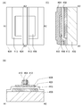
本発明の一態様は、第1の絶縁体上に酸化物半導体を形成し、第1の絶縁体上および酸化物半導体上に第2の絶縁体を成膜し、第2の絶縁体上に第1の導電体を成膜し、第1の導電体上にエッチングマスクを形成し、エッチングマスクをマスクとして第1の導電体をエッチングすることで、酸化物半導体と重なる領域を有する第2の導電体を形成し、エッチングマスクを除去し、第2の絶縁体上および第2の導電体上に水素含有層を成膜した後、加熱処理を行う半導体装置の作製方法である。
本発明の一態様は、(1)において、水素含有層の形成前に、第2の導電体の側面に接する第3の絶縁体を形成する半導体装置の作製方法である。
本発明の一態様は、(1)または(2)において、第2の絶縁体は酸化シリコンを有する半導体装置の作製方法である。
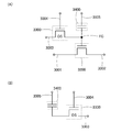
本発明の一態様は、第1の絶縁体上に第1の導電体を形成し、第1の絶縁体上および第1の導電体上に第2の絶縁体を成膜し、第2の絶縁体上に第1の酸化物半導体および第2の酸化物半導体を形成し、第2の絶縁体上および第1の酸化物半導体上に第3の絶縁体を形成し、第2の酸化物半導体上および第3の絶縁体上に第4の絶縁体を成膜し、第4の絶縁体上に水素含有層を成膜した後、加熱処理を行う半導体装置の作製方法である。
本発明の一態様は、(4)において、加熱処理の後、水素含有層を除去し、第4の絶縁体上に第2の導電体を成膜し、第2の導電体上にエッチングマスクを形成し、エッチングマスクをマスクとして第2の導電体をエッチングすることで、第2の酸化物半導体と重なる領域を有する第3の導電体を形成する半導体装置の作製方法である。
本発明の一態様は、(4)において、加熱処理の後、水素含有層上にエッチングマスクを形成し、エッチングマスクをマスクとして水素含有層をエッチングすることで、第2の酸化物半導体と重なる領域を有する水素含有層を形成する半導体装置の作製方法である。
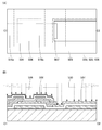
本発明の一態様は、(1)乃至(6)のいずれか一において、水素含有層は、二次イオン質量分析法において水素濃度が1×10²¹atoms/cm3以上5×1022atoms/cm3以下である半導体装置の作製方法である。
本発明の一態様は、(1)乃至(7)のいずれか一において、水素含有層は、非晶質シリコンを有する半導体装置の作製方法である。
以下では、図1を用いて、本発明の一態様に係る酸化物導電体の形成方法について説明する。
本発明の一態様に係る酸化物導電体をトランジスタに適用することができる。以下では、その一例を示す。
以下では、本発明の一態様に係るトランジスタの作製方法の変形例について説明する。
以下では、トランジスタの構成要素について説明する。
以下では酸化物半導体406に適用可能な酸化物について説明する。
以下では、酸化物半導体の構造について説明する。
まずは、CAAC−OSについて説明する。
次に、nc−OSについて説明する。
a−like OSは、nc−OSと非晶質酸化物半導体との間の構造を有する酸化物半導体である。
以下では、本発明の一態様に係る、トランジスタおよび容量素子を有する半導体装置の作製方法について説明する。
以下では、上述した半導体装置の一例として、フォトセンサを構成する場合について説明する。
以下では、本発明の一態様に係る半導体装置の回路の一例について説明する。
図25(A)に示す回路図は、pチャネル型のトランジスタ2200とnチャネル型のトランジスタ2100を直列に接続し、かつそれぞれのゲートを接続した、いわゆるCMOSインバータの構成を示している。
また図25(B)に示す回路図は、トランジスタ2100とトランジスタ2200のそれぞれのソースとドレインを接続した構成を示している。このような構成とすることで、いわゆるCMOSアナログスイッチとして機能させることができる。
本発明の一態様に係るトランジスタを用いた、電力が供給されない状況でも記憶内容の保持が可能で、かつ、書き込み回数にも制限が無い半導体装置(記憶装置)の一例を図26に示す。
図26(B)に示す半導体装置は、トランジスタ3200を有さない点で図26(A)に示した半導体装置と異なる。この場合も図26(A)に示した半導体装置と同様の動作により情報の書き込みおよび保持動作が可能である。
また本発明の一態様は、FPGA(Field Programmable Gate Array)などのLSIにも適用可能である。
以下では、上述したトランジスタや上述した記憶装置などの半導体装置を含むCPUについて説明する。
以下では、本発明の一態様に係る表示装置について、図30、図31および図51を用いて説明する。
以下では、単一の電源から電源電圧を昇圧または降圧し、各回路に分配する機能を有する半導体装置の一例について、図32乃至図38を用いて説明する。
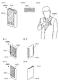
本発明の一態様に係る半導体装置は、表示機器、パーソナルコンピュータ、記録媒体を備えた画像再生装置(代表的にはDVD:Digital Versatile Disc等の記録媒体を再生し、その画像を表示しうるディスプレイを有する装置)に用いることができる。その他に、本発明の一態様に係る半導体装置を用いることができる電子機器として、携帯電話、携帯型を含むゲーム機、携帯データ端末、電子書籍端末、ビデオカメラ、デジタルスチルカメラ等のカメラ、ゴーグル型ディスプレイ(ヘッドマウントディスプレイ)、ナビゲーションシステム、音響再生装置(カーオーディオ、デジタルオーディオプレイヤー等)、複写機、ファクシミリ、プリンタ、プリンタ複合機、現金自動預け入れ払い機(ATM)、自動販売機などが挙げられる。これら電子機器の具体例を図39に示す。
以下では、本発明の一態様に係る電子機器の一例である表示領域または発光領域に曲面を有する電子機器について、図40を参照しながら説明する。なお、ここでは、電子機器の一例として、情報機器、特に携帯性を有する情報機器(携帯機器)について説明する。携帯性を有する情報機器としては、例えば、携帯電話機(ファブレット、スマートフォン(スマホ))、タブレット端末(スレートPC)なども含まれる。
携帯機器1300Aは、例えば電話、電子メール作成閲覧、手帳または情報閲覧などの機能から選ばれた一つまたは複数の機能を有する。

105a 欠陥
105b 欠陥
106 酸化物半導体
107 過剰水素
109 酸化物導電体
114 絶縁体
400 基板
402 絶縁体
403 水素含有層
404 導電体
406 酸化物半導体
406i 領域
406n1 領域
406n2 領域
410 絶縁体
412 絶縁体
413 導電体
414 絶縁体
430 イオン
500 基板
503 水素含有層
503a 導電体
503b 導電体
504 導電体
505 導電体
506 酸化物半導体
507 酸化物半導体
507i 領域
507n 領域
508 保護層
512 絶縁体
513 導電体
514 導電体
516a 導電体
516b 導電体
516c 導電体
518 絶縁体
520 絶縁体
522 絶縁体
523i 層
523n 層
523p 層
524 導電体
525 導電体
528 絶縁体
530 イオン
550 トランジスタ
551 トランジスタ
552 トランジスタ
560 容量素子
580 フォトダイオード
700 基板
702 絶縁体
704 導電体
705 導電体
706a 酸化物絶縁体
706b 酸化物半導体
706c 酸化物絶縁体
707a 酸化物導電体
707b 酸化物導電体
707c 酸化物導電体
712a 絶縁体
712b 絶縁体
713a 導電体
713b 導電体
718 絶縁体
719 発光素子
731 端子
732 FPC
733a 配線
734 シール材
735 駆動回路
736 駆動回路
737 画素
741 トランジスタ
742 容量素子
743 スイッチ素子
744 信号線
750 基板
751 トランジスタ
752 容量素子
753 液晶素子
754 走査線
755 信号線
781 導電体
782 発光層
783 導電体
784 隔壁
791 導電体
792 絶縁体
793 液晶層
794 絶縁体
795 スペーサ
796 導電体
797 基板
801 半導体基板
802 基板
803 絶縁体
804 絶縁体
805 絶縁体
806 接着層
807 フィルタ
808 フィルタ
809 フィルタ
811 絶縁体
812 絶縁体
813 絶縁体
814 絶縁体
815 絶縁体
816 絶縁体
817 絶縁体
818 絶縁体
819 絶縁体
820 絶縁体
821 絶縁体
831 導電体
832 導電体
833 導電体
834 導電体
835 導電体
836 導電体
837 導電体
838 導電体
839 導電体
840 導電体
841 導電体
842 導電体
843 導電体
844 導電体
845 導電体
846 導電体
847 導電体
848 導電体
849 導電体
850 導電体
851 導電体
852 導電体
853 導電体
854 導電体
855 導電体
856 導電体
857 導電体
858 導電体
859 導電体
860 導電体
861 導電体
862 導電体
871 絶縁体
872 導電体
873 絶縁体
874 絶縁体
875 領域
876 領域
877 絶縁体
878 絶縁体
881 絶縁体
882 導電体
883 絶縁体
884 絶縁体
885 領域
886 領域
887 層
888 層
891 トランジスタ
892 トランジスタ
893 発光層
900 半導体装置
901 電源回路
902 回路
903 電圧生成回路
903A 電圧生成回路
903B 電圧生成回路
903C 電圧生成回路
903D 電圧生成回路
903E 電圧生成回路
904 回路
905 電圧生成回路
905A 電圧生成回路
905B 電圧生成回路
905C 電圧生成回路
905D 電圧生成回路
905E 電圧生成回路
906 回路
911 トランジスタ
912 トランジスタ
912A トランジスタ
912B トランジスタ
921 制御回路
922 トランジスタ
1189 ROMインターフェース
1190 基板
1191 ALU
1192 ALUコントローラ
1193 インストラクションデコーダ
1194 インタラプトコントローラ
1195 タイミングコントローラ
1196 レジスタ
1197 レジスタコントローラ
1198 バスインターフェース
1199 ROM
1200 記憶素子
1201 回路
1202 回路
1203 スイッチ
1204 スイッチ
1206 論理素子
1207 容量素子
1208 容量素子
1209 トランジスタ
1210 トランジスタ
1213 トランジスタ
1214 トランジスタ
1220 回路
1300A 携帯機器
1300B 携帯機器
1300C 携帯機器
1310 筐体
1311 領域
1312 領域
1521 ルーティングスイッチエレメント
1522 ロジックエレメント
1523 コンフィギュレーションメモリ
1524 ルックアップテーブル
1525 レジスタ
1526 セレクタ
1527 コンフィギュレーションメモリ
1601 筐体
1602 筐体
1603 表示部
1604 表示部
1605 マイクロフォン
1606 スピーカー
1607 操作キー
1608 スタイラス
1611 筐体
1612 筐体
1613 表示部
1614 表示部
1615 接続部
1616 操作キー
1621 筐体
1622 表示部
1623 キーボード
1624 ポインティングデバイス
1631 筐体
1632 冷蔵室用扉
1633 冷凍室用扉
1641 筐体
1642 筐体
1643 表示部
1644 操作キー
1645 レンズ
1646 接続部
1651 車体
1652 車輪
1653 ダッシュボード
1654 ライト
2054 フィルタ
2100 トランジスタ
2200 トランジスタ
3001 配線
3002 配線
3003 配線
3004 配線
3005 配線
3200 トランジスタ
3300 トランジスタ
3400 容量素子
Claims (3)
- 第1の絶縁体上に第1の導電体を形成し、
前記第1の絶縁体上および前記第1の導電体上に第2の絶縁体を成膜し、
前記第2の絶縁体上に第1の酸化物半導体および第2の酸化物半導体を形成し、
前記第2の絶縁体上および前記第1の酸化物半導体上に第3の絶縁体を形成し、
前記第2の酸化物半導体上および前記第3の絶縁体上に第4の絶縁体を成膜し、
前記第4の絶縁体上に水素含有層を成膜した後、加熱処理を行い、
前記加熱処理の後、前記水素含有層を除去し、
前記第4の絶縁体上に第2の導電体を成膜し、
前記第2の導電体をエッチングして、前記第2の酸化物半導体と重なる領域を有する第3の導電体を形成する半導体装置の作製方法。 - 請求項1において、
前記水素含有層は、二次イオン質量分析法において水素濃度が1×10²¹atoms/cm3以上5×1022atoms/cm3以下である半導体装置の作製方法。 - 請求項1又は請求項2において、
前記水素含有層は、非晶質シリコンを有する半導体装置の作製方法。
Applications Claiming Priority (2)
| Application Number | Priority Date | Filing Date | Title |
|---|---|---|---|
| JP2015206186 | 2015-10-20 | ||
| JP2015206186 | 2015-10-20 |
Publications (3)
| Publication Number | Publication Date |
|---|---|
| JP2017079330A JP2017079330A (ja) | 2017-04-27 |
| JP2017079330A5 JP2017079330A5 (ja) | 2019-11-28 |
| JP6851768B2 true JP6851768B2 (ja) | 2021-03-31 |
Family
ID=58524265
Family Applications (1)
| Application Number | Title | Priority Date | Filing Date |
|---|---|---|---|
| JP2016204232A Active JP6851768B2 (ja) | 2015-10-20 | 2016-10-18 | 半導体装置の作製方法 |
Country Status (2)
| Country | Link |
|---|---|
| US (1) | US9852926B2 (ja) |
| JP (1) | JP6851768B2 (ja) |
Families Citing this family (6)
| Publication number | Priority date | Publication date | Assignee | Title |
|---|---|---|---|---|
| WO2018211351A1 (en) | 2017-05-19 | 2018-11-22 | Semiconductor Energy Laboratory Co., Ltd. | Semiconductor device, display device, and method for manufacturing semiconductor device |
| WO2019135137A1 (ja) * | 2018-01-05 | 2019-07-11 | 株式会社半導体エネルギー研究所 | 半導体装置、及び半導体装置の作製方法 |
| CN108376695B (zh) * | 2018-02-05 | 2021-01-08 | 惠科股份有限公司 | 一种显示面板和显示装置 |
| JP7179517B2 (ja) * | 2018-03-01 | 2022-11-29 | Tianma Japan株式会社 | 表示装置 |
| JP7242633B2 (ja) * | 2018-03-16 | 2023-03-20 | 株式会社半導体エネルギー研究所 | 半導体装置、および半導体装置の作製方法 |
| US11069796B2 (en) | 2018-08-09 | 2021-07-20 | Semiconductor Energy Laboratory Co., Ltd. | Manufacturing method of semiconductor device |
Family Cites Families (138)
| Publication number | Priority date | Publication date | Assignee | Title |
|---|---|---|---|---|
| JPS60198861A (ja) | 1984-03-23 | 1985-10-08 | Fujitsu Ltd | 薄膜トランジスタ |
| JPH0244256B2 (ja) | 1987-01-28 | 1990-10-03 | Kagaku Gijutsucho Mukizaishitsu Kenkyushocho | Ingazn2o5deshimesarerurotsuhoshokeinosojokozoojusurukagobutsuoyobisonoseizoho |
| JPH0244258B2 (ja) | 1987-02-24 | 1990-10-03 | Kagaku Gijutsucho Mukizaishitsu Kenkyushocho | Ingazn3o6deshimesarerurotsuhoshokeinosojokozoojusurukagobutsuoyobisonoseizoho |
| JPH0244260B2 (ja) | 1987-02-24 | 1990-10-03 | Kagaku Gijutsucho Mukizaishitsu Kenkyushocho | Ingazn5o8deshimesarerurotsuhoshokeinosojokozoojusurukagobutsuoyobisonoseizoho |
| JPS63210023A (ja) | 1987-02-24 | 1988-08-31 | Natl Inst For Res In Inorg Mater | InGaZn↓4O↓7で示される六方晶系の層状構造を有する化合物およびその製造法 |
| JPH0244262B2 (ja) | 1987-02-27 | 1990-10-03 | Kagaku Gijutsucho Mukizaishitsu Kenkyushocho | Ingazn6o9deshimesarerurotsuhoshokeinosojokozoojusurukagobutsuoyobisonoseizoho |
| JPH0244263B2 (ja) | 1987-04-22 | 1990-10-03 | Kagaku Gijutsucho Mukizaishitsu Kenkyushocho | Ingazn7o10deshimesarerurotsuhoshokeinosojokozoojusurukagobutsuoyobisonoseizoho |
| JPH05251705A (ja) | 1992-03-04 | 1993-09-28 | Fuji Xerox Co Ltd | 薄膜トランジスタ |
| JP3298974B2 (ja) | 1993-03-23 | 2002-07-08 | 電子科学株式会社 | 昇温脱離ガス分析装置 |
| JP3479375B2 (ja) | 1995-03-27 | 2003-12-15 | 科学技術振興事業団 | 亜酸化銅等の金属酸化物半導体による薄膜トランジスタとpn接合を形成した金属酸化物半導体装置およびそれらの製造方法 |
| DE69635107D1 (de) | 1995-08-03 | 2005-09-29 | Koninkl Philips Electronics Nv | Halbleiteranordnung mit einem transparenten schaltungselement |
| JP3625598B2 (ja) | 1995-12-30 | 2005-03-02 | 三星電子株式会社 | 液晶表示装置の製造方法 |
| JP4170454B2 (ja) | 1998-07-24 | 2008-10-22 | Hoya株式会社 | 透明導電性酸化物薄膜を有する物品及びその製造方法 |
| JP2000150861A (ja) | 1998-11-16 | 2000-05-30 | Tdk Corp | 酸化物薄膜 |
| JP3276930B2 (ja) | 1998-11-17 | 2002-04-22 | 科学技術振興事業団 | トランジスタ及び半導体装置 |
| TW460731B (en) | 1999-09-03 | 2001-10-21 | Ind Tech Res Inst | Electrode structure and production method of wide viewing angle LCD |
| JP4089858B2 (ja) | 2000-09-01 | 2008-05-28 | 国立大学法人東北大学 | 半導体デバイス |
| KR20020038482A (ko) | 2000-11-15 | 2002-05-23 | 모리시타 요이찌 | 박막 트랜지스터 어레이, 그 제조방법 및 그것을 이용한표시패널 |
| JP3997731B2 (ja) | 2001-03-19 | 2007-10-24 | 富士ゼロックス株式会社 | 基材上に結晶性半導体薄膜を形成する方法 |
| JP2002289859A (ja) | 2001-03-23 | 2002-10-04 | Minolta Co Ltd | 薄膜トランジスタ |
| JP4090716B2 (ja) | 2001-09-10 | 2008-05-28 | 雅司 川崎 | 薄膜トランジスタおよびマトリクス表示装置 |
| JP3925839B2 (ja) | 2001-09-10 | 2007-06-06 | シャープ株式会社 | 半導体記憶装置およびその試験方法 |
| JP4164562B2 (ja) | 2002-09-11 | 2008-10-15 | 独立行政法人科学技術振興機構 | ホモロガス薄膜を活性層として用いる透明薄膜電界効果型トランジスタ |
| EP1443130B1 (en) | 2001-11-05 | 2011-09-28 | Japan Science and Technology Agency | Natural superlattice homologous single crystal thin film, method for preparation thereof, and device using said single crystal thin film |
| JP4083486B2 (ja) | 2002-02-21 | 2008-04-30 | 独立行政法人科学技術振興機構 | LnCuO(S,Se,Te)単結晶薄膜の製造方法 |
| US7049190B2 (en) | 2002-03-15 | 2006-05-23 | Sanyo Electric Co., Ltd. | Method for forming ZnO film, method for forming ZnO semiconductor layer, method for fabricating semiconductor device, and semiconductor device |
| JP3933591B2 (ja) | 2002-03-26 | 2007-06-20 | 淳二 城戸 | 有機エレクトロルミネッセント素子 |
| US7339187B2 (en) | 2002-05-21 | 2008-03-04 | State Of Oregon Acting By And Through The Oregon State Board Of Higher Education On Behalf Of Oregon State University | Transistor structures |
| JP2004022625A (ja) | 2002-06-13 | 2004-01-22 | Murata Mfg Co Ltd | 半導体デバイス及び該半導体デバイスの製造方法 |
| US7105868B2 (en) | 2002-06-24 | 2006-09-12 | Cermet, Inc. | High-electron mobility transistor with zinc oxide |
| US7067843B2 (en) | 2002-10-11 | 2006-06-27 | E. I. Du Pont De Nemours And Company | Transparent oxide semiconductor thin film transistors |
| JP4166105B2 (ja) | 2003-03-06 | 2008-10-15 | シャープ株式会社 | 半導体装置およびその製造方法 |
| JP2004273732A (ja) | 2003-03-07 | 2004-09-30 | Sharp Corp | アクティブマトリクス基板およびその製造方法 |
| JP4108633B2 (ja) | 2003-06-20 | 2008-06-25 | シャープ株式会社 | 薄膜トランジスタおよびその製造方法ならびに電子デバイス |
| US7262463B2 (en) | 2003-07-25 | 2007-08-28 | Hewlett-Packard Development Company, L.P. | Transistor including a deposited channel region having a doped portion |
| US7297977B2 (en) | 2004-03-12 | 2007-11-20 | Hewlett-Packard Development Company, L.P. | Semiconductor device |
| US7145174B2 (en) | 2004-03-12 | 2006-12-05 | Hewlett-Packard Development Company, Lp. | Semiconductor device |
| EP2246894B2 (en) | 2004-03-12 | 2018-10-10 | Japan Science and Technology Agency | Method for fabricating a thin film transistor having an amorphous oxide as a channel layer |
| US7282782B2 (en) | 2004-03-12 | 2007-10-16 | Hewlett-Packard Development Company, L.P. | Combined binary oxide semiconductor device |
| US7211825B2 (en) | 2004-06-14 | 2007-05-01 | Yi-Chi Shih | Indium oxide-based thin film transistors and circuits |
| JP2006100760A (ja) | 2004-09-02 | 2006-04-13 | Casio Comput Co Ltd | 薄膜トランジスタおよびその製造方法 |
| US7285501B2 (en) | 2004-09-17 | 2007-10-23 | Hewlett-Packard Development Company, L.P. | Method of forming a solution processed device |
| US7298084B2 (en) | 2004-11-02 | 2007-11-20 | 3M Innovative Properties Company | Methods and displays utilizing integrated zinc oxide row and column drivers in conjunction with organic light emitting diodes |
| JP5118812B2 (ja) | 2004-11-10 | 2013-01-16 | キヤノン株式会社 | 電界効果型トランジスタ |
| RU2358354C2 (ru) | 2004-11-10 | 2009-06-10 | Кэнон Кабусики Кайся | Светоизлучающее устройство |
| US7453065B2 (en) | 2004-11-10 | 2008-11-18 | Canon Kabushiki Kaisha | Sensor and image pickup device |
| US7791072B2 (en) | 2004-11-10 | 2010-09-07 | Canon Kabushiki Kaisha | Display |
| KR100998527B1 (ko) | 2004-11-10 | 2010-12-07 | 고쿠리츠다이가쿠호진 토쿄고교 다이가꾸 | 비정질 산화물 및 전계 효과 트랜지스터 |
| US7829444B2 (en) | 2004-11-10 | 2010-11-09 | Canon Kabushiki Kaisha | Field effect transistor manufacturing method |
| US7863611B2 (en) | 2004-11-10 | 2011-01-04 | Canon Kabushiki Kaisha | Integrated circuits utilizing amorphous oxides |
| US7579224B2 (en) | 2005-01-21 | 2009-08-25 | Semiconductor Energy Laboratory Co., Ltd. | Method for manufacturing a thin film semiconductor device |
| TWI562380B (en) | 2005-01-28 | 2016-12-11 | Semiconductor Energy Lab Co Ltd | Semiconductor device, electronic device, and method of manufacturing semiconductor device |
| US7608531B2 (en) | 2005-01-28 | 2009-10-27 | Semiconductor Energy Laboratory Co., Ltd. | Semiconductor device, electronic device, and method of manufacturing semiconductor device |
| US7858451B2 (en) | 2005-02-03 | 2010-12-28 | Semiconductor Energy Laboratory Co., Ltd. | Electronic device, semiconductor device and manufacturing method thereof |
| US7948171B2 (en) | 2005-02-18 | 2011-05-24 | Semiconductor Energy Laboratory Co., Ltd. | Light emitting device |
| US20060197092A1 (en) | 2005-03-03 | 2006-09-07 | Randy Hoffman | System and method for forming conductive material on a substrate |
| US8681077B2 (en) | 2005-03-18 | 2014-03-25 | Semiconductor Energy Laboratory Co., Ltd. | Semiconductor device, and display device, driving method and electronic apparatus thereof |
| WO2006105077A2 (en) | 2005-03-28 | 2006-10-05 | Massachusetts Institute Of Technology | Low voltage thin film transistor with high-k dielectric material |
| US7645478B2 (en) | 2005-03-31 | 2010-01-12 | 3M Innovative Properties Company | Methods of making displays |
| US8300031B2 (en) | 2005-04-20 | 2012-10-30 | Semiconductor Energy Laboratory Co., Ltd. | Semiconductor device comprising transistor having gate and drain connected through a current-voltage conversion element |
| JP2006344849A (ja) | 2005-06-10 | 2006-12-21 | Casio Comput Co Ltd | 薄膜トランジスタ |
| US7691666B2 (en) | 2005-06-16 | 2010-04-06 | Eastman Kodak Company | Methods of making thin film transistors comprising zinc-oxide-based semiconductor materials and transistors made thereby |
| US7402506B2 (en) | 2005-06-16 | 2008-07-22 | Eastman Kodak Company | Methods of making thin film transistors comprising zinc-oxide-based semiconductor materials and transistors made thereby |
| US7507618B2 (en) | 2005-06-27 | 2009-03-24 | 3M Innovative Properties Company | Method for making electronic devices using metal oxide nanoparticles |
| KR100711890B1 (ko) | 2005-07-28 | 2007-04-25 | 삼성에스디아이 주식회사 | 유기 발광표시장치 및 그의 제조방법 |
| JP2007059128A (ja) | 2005-08-23 | 2007-03-08 | Canon Inc | 有機el表示装置およびその製造方法 |
| JP4280736B2 (ja) | 2005-09-06 | 2009-06-17 | キヤノン株式会社 | 半導体素子 |
| JP4850457B2 (ja) | 2005-09-06 | 2012-01-11 | キヤノン株式会社 | 薄膜トランジスタ及び薄膜ダイオード |
| JP2007073705A (ja) | 2005-09-06 | 2007-03-22 | Canon Inc | 酸化物半導体チャネル薄膜トランジスタおよびその製造方法 |
| JP5116225B2 (ja) | 2005-09-06 | 2013-01-09 | キヤノン株式会社 | 酸化物半導体デバイスの製造方法 |
| EP1998375A3 (en) | 2005-09-29 | 2012-01-18 | Semiconductor Energy Laboratory Co, Ltd. | Semiconductor device having oxide semiconductor layer and manufacturing method |
| JP5037808B2 (ja) | 2005-10-20 | 2012-10-03 | キヤノン株式会社 | アモルファス酸化物を用いた電界効果型トランジスタ、及び該トランジスタを用いた表示装置 |
| KR101358954B1 (ko) | 2005-11-15 | 2014-02-06 | 가부시키가이샤 한도오따이 에네루기 켄큐쇼 | 다이오드 및 액티브 매트릭스 표시장치 |
| TWI292281B (en) | 2005-12-29 | 2008-01-01 | Ind Tech Res Inst | Pixel structure of active organic light emitting diode and method of fabricating the same |
| US7867636B2 (en) | 2006-01-11 | 2011-01-11 | Murata Manufacturing Co., Ltd. | Transparent conductive film and method for manufacturing the same |
| JP4977478B2 (ja) | 2006-01-21 | 2012-07-18 | 三星電子株式会社 | ZnOフィルム及びこれを用いたTFTの製造方法 |
| US7576394B2 (en) | 2006-02-02 | 2009-08-18 | Kochi Industrial Promotion Center | Thin film transistor including low resistance conductive thin films and manufacturing method thereof |
| JP5015471B2 (ja) * | 2006-02-15 | 2012-08-29 | 財団法人高知県産業振興センター | 薄膜トランジスタ及びその製法 |
| US7977169B2 (en) | 2006-02-15 | 2011-07-12 | Kochi Industrial Promotion Center | Semiconductor device including active layer made of zinc oxide with controlled orientations and manufacturing method thereof |
| KR20070101595A (ko) | 2006-04-11 | 2007-10-17 | 삼성전자주식회사 | ZnO TFT |
| US20070252928A1 (en) | 2006-04-28 | 2007-11-01 | Toppan Printing Co., Ltd. | Structure, transmission type liquid crystal display, reflection type display and manufacturing method thereof |
| JP5028033B2 (ja) | 2006-06-13 | 2012-09-19 | キヤノン株式会社 | 酸化物半導体膜のドライエッチング方法 |
| JP4999400B2 (ja) | 2006-08-09 | 2012-08-15 | キヤノン株式会社 | 酸化物半導体膜のドライエッチング方法 |
| JP4609797B2 (ja) | 2006-08-09 | 2011-01-12 | Nec液晶テクノロジー株式会社 | 薄膜デバイス及びその製造方法 |
| JP4332545B2 (ja) | 2006-09-15 | 2009-09-16 | キヤノン株式会社 | 電界効果型トランジスタ及びその製造方法 |
| JP5164357B2 (ja) | 2006-09-27 | 2013-03-21 | キヤノン株式会社 | 半導体装置及び半導体装置の製造方法 |
| JP4274219B2 (ja) | 2006-09-27 | 2009-06-03 | セイコーエプソン株式会社 | 電子デバイス、有機エレクトロルミネッセンス装置、有機薄膜半導体装置 |
| US7622371B2 (en) | 2006-10-10 | 2009-11-24 | Hewlett-Packard Development Company, L.P. | Fused nanocrystal thin film semiconductor and method |
| US7772021B2 (en) | 2006-11-29 | 2010-08-10 | Samsung Electronics Co., Ltd. | Flat panel displays comprising a thin-film transistor having a semiconductive oxide in its channel and methods of fabricating the same for use in flat panel displays |
| JP2008140684A (ja) | 2006-12-04 | 2008-06-19 | Toppan Printing Co Ltd | カラーelディスプレイおよびその製造方法 |
| KR101303578B1 (ko) | 2007-01-05 | 2013-09-09 | 삼성전자주식회사 | 박막 식각 방법 |
| US8207063B2 (en) | 2007-01-26 | 2012-06-26 | Eastman Kodak Company | Process for atomic layer deposition |
| KR100851215B1 (ko) | 2007-03-14 | 2008-08-07 | 삼성에스디아이 주식회사 | 박막 트랜지스터 및 이를 이용한 유기 전계 발광표시장치 |
| US7795613B2 (en) | 2007-04-17 | 2010-09-14 | Toppan Printing Co., Ltd. | Structure with transistor |
| KR101325053B1 (ko) | 2007-04-18 | 2013-11-05 | 삼성디스플레이 주식회사 | 박막 트랜지스터 기판 및 이의 제조 방법 |
| KR20080094300A (ko) | 2007-04-19 | 2008-10-23 | 삼성전자주식회사 | 박막 트랜지스터 및 그 제조 방법과 박막 트랜지스터를포함하는 평판 디스플레이 |
| KR101334181B1 (ko) | 2007-04-20 | 2013-11-28 | 삼성전자주식회사 | 선택적으로 결정화된 채널층을 갖는 박막 트랜지스터 및 그제조 방법 |
| CN101663762B (zh) | 2007-04-25 | 2011-09-21 | 佳能株式会社 | 氧氮化物半导体 |
| KR101345376B1 (ko) | 2007-05-29 | 2013-12-24 | 삼성전자주식회사 | ZnO 계 박막 트랜지스터 및 그 제조방법 |
| US8202365B2 (en) | 2007-12-17 | 2012-06-19 | Fujifilm Corporation | Process for producing oriented inorganic crystalline film, and semiconductor device using the oriented inorganic crystalline film |
| JP4623179B2 (ja) | 2008-09-18 | 2011-02-02 | ソニー株式会社 | 薄膜トランジスタおよびその製造方法 |
| JP5451280B2 (ja) | 2008-10-09 | 2014-03-26 | キヤノン株式会社 | ウルツ鉱型結晶成長用基板およびその製造方法ならびに半導体装置 |
| CN105679766A (zh) | 2009-09-16 | 2016-06-15 | 株式会社半导体能源研究所 | 晶体管及显示设备 |
| KR101892430B1 (ko) * | 2009-10-21 | 2018-08-30 | 가부시키가이샤 한도오따이 에네루기 켄큐쇼 | 반도체 장치 |
| US8634230B2 (en) * | 2011-01-28 | 2014-01-21 | Semiconductor Energy Laboratory Co., Ltd. | Semiconductor device and method for driving the same |
| KR102099445B1 (ko) * | 2012-06-29 | 2020-04-09 | 가부시키가이샤 한도오따이 에네루기 켄큐쇼 | 반도체 장치 및 반도체 장치의 제작 방법 |
| KR20230175323A (ko) * | 2012-09-13 | 2023-12-29 | 가부시키가이샤 한도오따이 에네루기 켄큐쇼 | 표시 장치 |
| KR102211215B1 (ko) * | 2012-09-14 | 2021-02-02 | 가부시키가이샤 한도오따이 에네루기 켄큐쇼 | 반도체 장치 및 그 제작 방법 |
| JP2014093433A (ja) * | 2012-11-05 | 2014-05-19 | Sony Corp | 半導体装置、表示装置および電子機器 |
| KR102241249B1 (ko) | 2012-12-25 | 2021-04-15 | 가부시키가이샤 한도오따이 에네루기 켄큐쇼 | 저항 소자, 표시 장치, 및 전자기기 |
| US9293544B2 (en) * | 2013-02-26 | 2016-03-22 | Semiconductor Energy Laboratory Co., Ltd. | Semiconductor device having buried channel structure |
| TWI651839B (zh) | 2013-02-27 | 2019-02-21 | 半導體能源研究所股份有限公司 | 半導體裝置、驅動電路及顯示裝置 |
| TWI635613B (zh) | 2013-04-03 | 2018-09-11 | 半導體能源研究所股份有限公司 | 半導體裝置 |
| US20140306219A1 (en) | 2013-04-10 | 2014-10-16 | Semiconductor Energy Laboratory Co., Ltd. | Semiconductor device |
| US9704894B2 (en) * | 2013-05-10 | 2017-07-11 | Semiconductor Energy Laboratory Co., Ltd. | Display device including pixel electrode including oxide |
| KR102244553B1 (ko) * | 2013-08-23 | 2021-04-23 | 가부시키가이샤 한도오따이 에네루기 켄큐쇼 | 용량 소자 및 반도체 장치 |
| TW202334724A (zh) | 2013-08-28 | 2023-09-01 | 日商半導體能源研究所股份有限公司 | 顯示裝置 |
| CN110806663A (zh) | 2013-09-13 | 2020-02-18 | 株式会社半导体能源研究所 | 显示装置 |
| DE112014004839T5 (de) | 2013-10-22 | 2016-07-07 | Semiconductor Energy Laboratory Co., Ltd. | Anzeigevorrichtung |
| JP2016001712A (ja) | 2013-11-29 | 2016-01-07 | 株式会社半導体エネルギー研究所 | 半導体装置の作製方法 |
| JP6496132B2 (ja) * | 2013-12-02 | 2019-04-03 | 株式会社半導体エネルギー研究所 | 半導体装置 |
| JP2016027597A (ja) * | 2013-12-06 | 2016-02-18 | 株式会社半導体エネルギー研究所 | 半導体装置 |
| JP6468686B2 (ja) | 2014-04-25 | 2019-02-13 | 株式会社半導体エネルギー研究所 | 入出力装置 |
| KR102333604B1 (ko) | 2014-05-15 | 2021-11-30 | 가부시키가이샤 한도오따이 에네루기 켄큐쇼 | 반도체 장치, 이 반도체 장치를 포함하는 표시 장치 |
| US10002971B2 (en) | 2014-07-03 | 2018-06-19 | Semiconductor Energy Laboratory Co., Ltd. | Semiconductor device and display device including the semiconductor device |
| US9766517B2 (en) | 2014-09-05 | 2017-09-19 | Semiconductor Energy Laboratory Co., Ltd. | Display device and display module |
| WO2016108122A1 (en) | 2014-12-29 | 2016-07-07 | Semiconductor Energy Laboratory Co., Ltd. | Semiconductor device and display device having semiconductor device |
| CN113223967A (zh) | 2015-03-03 | 2021-08-06 | 株式会社半导体能源研究所 | 半导体装置、该半导体装置的制造方法或包括该半导体装置的显示装置 |
| US10008609B2 (en) | 2015-03-17 | 2018-06-26 | Semiconductor Energy Laboratory Co., Ltd. | Semiconductor device, method for manufacturing the same, or display device including the same |
| CN107430461B (zh) | 2015-03-17 | 2022-01-28 | 株式会社半导体能源研究所 | 触摸屏 |
| JP6662665B2 (ja) | 2015-03-19 | 2020-03-11 | 株式会社半導体エネルギー研究所 | 液晶表示装置及び該液晶表示装置を用いた電子機器 |
| US10002970B2 (en) | 2015-04-30 | 2018-06-19 | Semiconductor Energy Laboratory Co., Ltd. | Semiconductor device, manufacturing method of the same, or display device including the same |
| KR20240014632A (ko) | 2015-05-22 | 2024-02-01 | 가부시키가이샤 한도오따이 에네루기 켄큐쇼 | 반도체 장치, 및 상기 반도체 장치를 포함하는 표시 장치 |
| JP6832634B2 (ja) | 2015-05-29 | 2021-02-24 | 株式会社半導体エネルギー研究所 | 半導体装置 |
| US10501003B2 (en) | 2015-07-17 | 2019-12-10 | Semiconductor Energy Laboratory Co., Ltd. | Semiconductor device, lighting device, and vehicle |
| KR20170031620A (ko) | 2015-09-11 | 2017-03-21 | 가부시키가이샤 한도오따이 에네루기 켄큐쇼 | 표시 장치 및 그 제작 방법 |
| JP2017076788A (ja) | 2015-10-12 | 2017-04-20 | 株式会社半導体エネルギー研究所 | 半導体装置の作製方法 |
| WO2017064590A1 (en) | 2015-10-12 | 2017-04-20 | Semiconductor Energy Laboratory Co., Ltd. | Method for manufacturing semiconductor device |
-
2016
- 2016-10-17 US US15/295,016 patent/US9852926B2/en not_active Expired - Fee Related
- 2016-10-18 JP JP2016204232A patent/JP6851768B2/ja active Active
Also Published As
| Publication number | Publication date |
|---|---|
| JP2017079330A (ja) | 2017-04-27 |
| US9852926B2 (en) | 2017-12-26 |
| US20170110337A1 (en) | 2017-04-20 |
Similar Documents
| Publication | Publication Date | Title |
|---|---|---|
| JP6841945B2 (ja) | 表示装置 | |
| JP6945976B2 (ja) | 半導体装置の作製方法 | |
| JP6796411B2 (ja) | 半導体装置の作製方法 | |
| JP6851768B2 (ja) | 半導体装置の作製方法 | |
| JP7457074B2 (ja) | 半導体装置 | |
| JP6764681B2 (ja) | 半導体装置の作製方法 | |
| TWI699835B (zh) | 半導體裝置、其製造方法以及電子裝置 | |
| JP6839986B2 (ja) | 半導体装置の作製方法 | |
| JP7095134B2 (ja) | 半導体装置の作製方法 | |
| JP2021132236A (ja) | 半導体装置 | |
| JP2020161845A (ja) | 電子機器 | |
| JP2021170651A (ja) | 半導体装置 | |
| JP2021132229A (ja) | 半導体装置 | |
| TW202013748A (zh) | 半導體裝置及包括該半導體裝置的電子裝置 | |
| JP2016164979A (ja) | 半導体装置およびその作製方法 | |
| JP2022068260A (ja) | 半導体装置 | |
| JP2021108407A (ja) | 半導体装置 | |
| JP6773423B2 (ja) | 半導体装置 | |
| JP6828119B2 (ja) | 表示装置 | |
| US20160056043A1 (en) | Semiconductor Device, Method for Manufacturing Semiconductor Device, and Electronic Appliance Having Semiconductor Device | |
| JP2022000934A (ja) | 半導体装置 | |
| TWI672812B (zh) | 半導體裝置、模組及電子裝置 | |
| JP2021093554A (ja) | 半導体装置 | |
| JP2021170665A (ja) | 半導体装置 |
Legal Events
| Date | Code | Title | Description |
|---|---|---|---|
| A521 | Request for written amendment filed |
Free format text: JAPANESE INTERMEDIATE CODE: A523 Effective date: 20191015 |
|
| A621 | Written request for application examination |
Free format text: JAPANESE INTERMEDIATE CODE: A621 Effective date: 20191015 |
|
| A977 | Report on retrieval |
Free format text: JAPANESE INTERMEDIATE CODE: A971007 Effective date: 20201022 |
|
| A131 | Notification of reasons for refusal |
Free format text: JAPANESE INTERMEDIATE CODE: A131 Effective date: 20201027 |
|
| A521 | Request for written amendment filed |
Free format text: JAPANESE INTERMEDIATE CODE: A523 Effective date: 20201221 |
|
| TRDD | Decision of grant or rejection written | ||
| A01 | Written decision to grant a patent or to grant a registration (utility model) |
Free format text: JAPANESE INTERMEDIATE CODE: A01 Effective date: 20210216 |
|
| A61 | First payment of annual fees (during grant procedure) |
Free format text: JAPANESE INTERMEDIATE CODE: A61 Effective date: 20210310 |
|
| R150 | Certificate of patent or registration of utility model |
Ref document number: 6851768 Country of ref document: JP Free format text: JAPANESE INTERMEDIATE CODE: R150 |