JP6725055B2 - 半導体装置および半導体装置の製造方法 - Google Patents
半導体装置および半導体装置の製造方法 Download PDFInfo
- Publication number
- JP6725055B2 JP6725055B2 JP2019500070A JP2019500070A JP6725055B2 JP 6725055 B2 JP6725055 B2 JP 6725055B2 JP 2019500070 A JP2019500070 A JP 2019500070A JP 2019500070 A JP2019500070 A JP 2019500070A JP 6725055 B2 JP6725055 B2 JP 6725055B2
- Authority
- JP
- Japan
- Prior art keywords
- region
- drift region
- semiconductor device
- substrate
- gate
- Prior art date
- Legal status (The legal status is an assumption and is not a legal conclusion. Google has not performed a legal analysis and makes no representation as to the accuracy of the status listed.)
- Active
Links
- 239000004065 semiconductor Substances 0.000 title claims description 228
- 238000004519 manufacturing process Methods 0.000 title claims description 53
- 239000000758 substrate Substances 0.000 claims description 167
- 238000000034 method Methods 0.000 claims description 115
- 239000012535 impurity Substances 0.000 claims description 82
- 238000005468 ion implantation Methods 0.000 claims description 30
- 230000003213 activating effect Effects 0.000 claims description 2
- 239000000463 material Substances 0.000 description 79
- 230000004048 modification Effects 0.000 description 68
- 238000012986 modification Methods 0.000 description 68
- 238000005530 etching Methods 0.000 description 57
- 229910021420 polycrystalline silicon Inorganic materials 0.000 description 56
- 229920005591 polysilicon Polymers 0.000 description 55
- 239000010936 titanium Substances 0.000 description 46
- KRHYYFGTRYWZRS-UHFFFAOYSA-N Fluorane Chemical compound F KRHYYFGTRYWZRS-UHFFFAOYSA-N 0.000 description 44
- 238000000151 deposition Methods 0.000 description 40
- 239000011229 interlayer Substances 0.000 description 40
- HBMJWWWQQXIZIP-UHFFFAOYSA-N silicon carbide Chemical compound [Si+]#[C-] HBMJWWWQQXIZIP-UHFFFAOYSA-N 0.000 description 37
- 238000002513 implantation Methods 0.000 description 36
- IJGRMHOSHXDMSA-UHFFFAOYSA-N Atomic nitrogen Chemical compound N#N IJGRMHOSHXDMSA-UHFFFAOYSA-N 0.000 description 28
- PXHVJJICTQNCMI-UHFFFAOYSA-N Nickel Chemical compound [Ni] PXHVJJICTQNCMI-UHFFFAOYSA-N 0.000 description 28
- VYPSYNLAJGMNEJ-UHFFFAOYSA-N Silicium dioxide Chemical compound O=[Si]=O VYPSYNLAJGMNEJ-UHFFFAOYSA-N 0.000 description 27
- 229910052814 silicon oxide Inorganic materials 0.000 description 27
- 229910010271 silicon carbide Inorganic materials 0.000 description 25
- 229910052719 titanium Inorganic materials 0.000 description 24
- RTAQQCXQSZGOHL-UHFFFAOYSA-N Titanium Chemical compound [Ti] RTAQQCXQSZGOHL-UHFFFAOYSA-N 0.000 description 22
- 239000010410 layer Substances 0.000 description 21
- 230000003647 oxidation Effects 0.000 description 20
- 238000007254 oxidation reaction Methods 0.000 description 20
- QVGXLLKOCUKJST-UHFFFAOYSA-N atomic oxygen Chemical compound [O] QVGXLLKOCUKJST-UHFFFAOYSA-N 0.000 description 19
- 230000005684 electric field Effects 0.000 description 19
- 239000001301 oxygen Substances 0.000 description 19
- 229910052760 oxygen Inorganic materials 0.000 description 19
- XKRFYHLGVUSROY-UHFFFAOYSA-N Argon Chemical compound [Ar] XKRFYHLGVUSROY-UHFFFAOYSA-N 0.000 description 18
- QAOWNCQODCNURD-UHFFFAOYSA-N Sulfuric acid Chemical compound OS(O)(=O)=O QAOWNCQODCNURD-UHFFFAOYSA-N 0.000 description 18
- 238000001312 dry etching Methods 0.000 description 17
- 229910052751 metal Inorganic materials 0.000 description 16
- 239000002184 metal Substances 0.000 description 16
- 230000015556 catabolic process Effects 0.000 description 14
- 229910052757 nitrogen Inorganic materials 0.000 description 14
- 238000000059 patterning Methods 0.000 description 14
- 238000005268 plasma chemical vapour deposition Methods 0.000 description 14
- 238000002230 thermal chemical vapour deposition Methods 0.000 description 14
- 150000002500 ions Chemical class 0.000 description 13
- 238000000206 photolithography Methods 0.000 description 13
- 238000001020 plasma etching Methods 0.000 description 13
- 238000001039 wet etching Methods 0.000 description 13
- 238000010438 heat treatment Methods 0.000 description 12
- MWUXSHHQAYIFBG-UHFFFAOYSA-N Nitric oxide Chemical compound O=[N] MWUXSHHQAYIFBG-UHFFFAOYSA-N 0.000 description 10
- GQPLMRYTRLFLPF-UHFFFAOYSA-N Nitrous Oxide Chemical compound [O-][N+]#N GQPLMRYTRLFLPF-UHFFFAOYSA-N 0.000 description 10
- 229910052786 argon Inorganic materials 0.000 description 9
- 229910052750 molybdenum Inorganic materials 0.000 description 9
- 229910052759 nickel Inorganic materials 0.000 description 9
- ZOKXTWBITQBERF-UHFFFAOYSA-N Molybdenum Chemical compound [Mo] ZOKXTWBITQBERF-UHFFFAOYSA-N 0.000 description 7
- 239000011733 molybdenum Substances 0.000 description 7
- 238000000137 annealing Methods 0.000 description 6
- 239000000969 carrier Substances 0.000 description 6
- 239000004020 conductor Substances 0.000 description 6
- 238000001816 cooling Methods 0.000 description 5
- 239000013078 crystal Substances 0.000 description 5
- 238000010586 diagram Methods 0.000 description 5
- 239000007772 electrode material Substances 0.000 description 5
- 238000004518 low pressure chemical vapour deposition Methods 0.000 description 5
- 229960001730 nitrous oxide Drugs 0.000 description 5
- 235000013842 nitrous oxide Nutrition 0.000 description 5
- 238000004544 sputter deposition Methods 0.000 description 5
- ZOXJGFHDIHLPTG-UHFFFAOYSA-N Boron Chemical compound [B] ZOXJGFHDIHLPTG-UHFFFAOYSA-N 0.000 description 4
- 229910052782 aluminium Inorganic materials 0.000 description 4
- XAGFODPZIPBFFR-UHFFFAOYSA-N aluminium Chemical compound [Al] XAGFODPZIPBFFR-UHFFFAOYSA-N 0.000 description 4
- 229910052796 boron Inorganic materials 0.000 description 4
- 238000004140 cleaning Methods 0.000 description 4
- 230000007547 defect Effects 0.000 description 4
- RLOWWWKZYUNIDI-UHFFFAOYSA-N phosphinic chloride Chemical compound ClP=O RLOWWWKZYUNIDI-UHFFFAOYSA-N 0.000 description 4
- 230000015572 biosynthetic process Effects 0.000 description 3
- 239000007943 implant Substances 0.000 description 3
- 229910052581 Si3N4 Inorganic materials 0.000 description 2
- 230000007423 decrease Effects 0.000 description 2
- 238000009826 distribution Methods 0.000 description 2
- 230000000694 effects Effects 0.000 description 2
- 230000007257 malfunction Effects 0.000 description 2
- QPJSUIGXIBEQAC-UHFFFAOYSA-N n-(2,4-dichloro-5-propan-2-yloxyphenyl)acetamide Chemical compound CC(C)OC1=CC(NC(C)=O)=C(Cl)C=C1Cl QPJSUIGXIBEQAC-UHFFFAOYSA-N 0.000 description 2
- XHXFXVLFKHQFAL-UHFFFAOYSA-N phosphoryl trichloride Chemical compound ClP(Cl)(Cl)=O XHXFXVLFKHQFAL-UHFFFAOYSA-N 0.000 description 2
- HQVNEWCFYHHQES-UHFFFAOYSA-N silicon nitride Chemical compound N12[Si]34N5[Si]62N3[Si]51N64 HQVNEWCFYHHQES-UHFFFAOYSA-N 0.000 description 2
- 229910002704 AlGaN Inorganic materials 0.000 description 1
- 229910002601 GaN Inorganic materials 0.000 description 1
- 229910004298 SiO 2 Inorganic materials 0.000 description 1
- XUIMIQQOPSSXEZ-UHFFFAOYSA-N Silicon Chemical compound [Si] XUIMIQQOPSSXEZ-UHFFFAOYSA-N 0.000 description 1
- 229910000577 Silicon-germanium Inorganic materials 0.000 description 1
- 238000005452 bending Methods 0.000 description 1
- 230000008021 deposition Effects 0.000 description 1
- 229910003460 diamond Inorganic materials 0.000 description 1
- 239000010432 diamond Substances 0.000 description 1
- 230000005669 field effect Effects 0.000 description 1
- 230000012447 hatching Effects 0.000 description 1
- 239000011810 insulating material Substances 0.000 description 1
- 238000009413 insulation Methods 0.000 description 1
- 229910044991 metal oxide Inorganic materials 0.000 description 1
- 150000004706 metal oxides Chemical class 0.000 description 1
- 230000002093 peripheral effect Effects 0.000 description 1
- 102000054765 polymorphisms of proteins Human genes 0.000 description 1
- 229910052710 silicon Inorganic materials 0.000 description 1
- 239000010703 silicon Substances 0.000 description 1
- XLOMVQKBTHCTTD-UHFFFAOYSA-N zinc oxide Inorganic materials [Zn]=O XLOMVQKBTHCTTD-UHFFFAOYSA-N 0.000 description 1
Images


Classifications
-
- H—ELECTRICITY
- H01—ELECTRIC ELEMENTS
- H01L—SEMICONDUCTOR DEVICES NOT COVERED BY CLASS H10
- H01L29/00—Semiconductor devices adapted for rectifying, amplifying, oscillating or switching, or capacitors or resistors with at least one potential-jump barrier or surface barrier, e.g. PN junction depletion layer or carrier concentration layer; Details of semiconductor bodies or of electrodes thereof ; Multistep manufacturing processes therefor
- H01L29/02—Semiconductor bodies ; Multistep manufacturing processes therefor
- H01L29/06—Semiconductor bodies ; Multistep manufacturing processes therefor characterised by their shape; characterised by the shapes, relative sizes, or dispositions of the semiconductor regions ; characterised by the concentration or distribution of impurities within semiconductor regions
- H01L29/08—Semiconductor bodies ; Multistep manufacturing processes therefor characterised by their shape; characterised by the shapes, relative sizes, or dispositions of the semiconductor regions ; characterised by the concentration or distribution of impurities within semiconductor regions with semiconductor regions connected to an electrode carrying current to be rectified, amplified or switched and such electrode being part of a semiconductor device which comprises three or more electrodes
- H01L29/0843—Source or drain regions of field-effect devices
- H01L29/0847—Source or drain regions of field-effect devices of field-effect transistors with insulated gate
- H01L29/0852—Source or drain regions of field-effect devices of field-effect transistors with insulated gate of DMOS transistors
- H01L29/0873—Drain regions
- H01L29/0882—Disposition
-
- H—ELECTRICITY
- H01—ELECTRIC ELEMENTS
- H01L—SEMICONDUCTOR DEVICES NOT COVERED BY CLASS H10
- H01L21/00—Processes or apparatus adapted for the manufacture or treatment of semiconductor or solid state devices or of parts thereof
- H01L21/02—Manufacture or treatment of semiconductor devices or of parts thereof
- H01L21/04—Manufacture or treatment of semiconductor devices or of parts thereof the devices having at least one potential-jump barrier or surface barrier, e.g. PN junction, depletion layer or carrier concentration layer
- H01L21/0445—Manufacture or treatment of semiconductor devices or of parts thereof the devices having at least one potential-jump barrier or surface barrier, e.g. PN junction, depletion layer or carrier concentration layer the devices having semiconductor bodies comprising crystalline silicon carbide
- H01L21/0455—Making n or p doped regions or layers, e.g. using diffusion
- H01L21/046—Making n or p doped regions or layers, e.g. using diffusion using ion implantation
- H01L21/0465—Making n or p doped regions or layers, e.g. using diffusion using ion implantation using masks
-
- H—ELECTRICITY
- H01—ELECTRIC ELEMENTS
- H01L—SEMICONDUCTOR DEVICES NOT COVERED BY CLASS H10
- H01L29/00—Semiconductor devices adapted for rectifying, amplifying, oscillating or switching, or capacitors or resistors with at least one potential-jump barrier or surface barrier, e.g. PN junction depletion layer or carrier concentration layer; Details of semiconductor bodies or of electrodes thereof ; Multistep manufacturing processes therefor
- H01L29/66—Types of semiconductor device ; Multistep manufacturing processes therefor
- H01L29/68—Types of semiconductor device ; Multistep manufacturing processes therefor controllable by only the electric current supplied, or only the electric potential applied, to an electrode which does not carry the current to be rectified, amplified or switched
- H01L29/76—Unipolar devices, e.g. field effect transistors
- H01L29/772—Field effect transistors
- H01L29/78—Field effect transistors with field effect produced by an insulated gate
- H01L29/7801—DMOS transistors, i.e. MISFETs with a channel accommodating body or base region adjoining a drain drift region
-
- H—ELECTRICITY
- H01—ELECTRIC ELEMENTS
- H01L—SEMICONDUCTOR DEVICES NOT COVERED BY CLASS H10
- H01L21/00—Processes or apparatus adapted for the manufacture or treatment of semiconductor or solid state devices or of parts thereof
- H01L21/02—Manufacture or treatment of semiconductor devices or of parts thereof
- H01L21/04—Manufacture or treatment of semiconductor devices or of parts thereof the devices having at least one potential-jump barrier or surface barrier, e.g. PN junction, depletion layer or carrier concentration layer
- H01L21/0445—Manufacture or treatment of semiconductor devices or of parts thereof the devices having at least one potential-jump barrier or surface barrier, e.g. PN junction, depletion layer or carrier concentration layer the devices having semiconductor bodies comprising crystalline silicon carbide
- H01L21/0455—Making n or p doped regions or layers, e.g. using diffusion
- H01L21/046—Making n or p doped regions or layers, e.g. using diffusion using ion implantation
- H01L21/047—Making n or p doped regions or layers, e.g. using diffusion using ion implantation characterised by the angle between the ion beam and the crystal planes or the main crystal surface
-
- H—ELECTRICITY
- H01—ELECTRIC ELEMENTS
- H01L—SEMICONDUCTOR DEVICES NOT COVERED BY CLASS H10
- H01L21/00—Processes or apparatus adapted for the manufacture or treatment of semiconductor or solid state devices or of parts thereof
- H01L21/70—Manufacture or treatment of devices consisting of a plurality of solid state components formed in or on a common substrate or of parts thereof; Manufacture of integrated circuit devices or of parts thereof
- H01L21/77—Manufacture or treatment of devices consisting of a plurality of solid state components or integrated circuits formed in, or on, a common substrate
- H01L21/78—Manufacture or treatment of devices consisting of a plurality of solid state components or integrated circuits formed in, or on, a common substrate with subsequent division of the substrate into plural individual devices
- H01L21/82—Manufacture or treatment of devices consisting of a plurality of solid state components or integrated circuits formed in, or on, a common substrate with subsequent division of the substrate into plural individual devices to produce devices, e.g. integrated circuits, each consisting of a plurality of components
- H01L21/822—Manufacture or treatment of devices consisting of a plurality of solid state components or integrated circuits formed in, or on, a common substrate with subsequent division of the substrate into plural individual devices to produce devices, e.g. integrated circuits, each consisting of a plurality of components the substrate being a semiconductor, using silicon technology
- H01L21/8232—Field-effect technology
- H01L21/8234—MIS technology, i.e. integration processes of field effect transistors of the conductor-insulator-semiconductor type
- H01L21/823418—MIS technology, i.e. integration processes of field effect transistors of the conductor-insulator-semiconductor type with a particular manufacturing method of the source or drain structures, e.g. specific source or drain implants or silicided source or drain structures or raised source or drain structures
-
- H—ELECTRICITY
- H01—ELECTRIC ELEMENTS
- H01L—SEMICONDUCTOR DEVICES NOT COVERED BY CLASS H10
- H01L21/00—Processes or apparatus adapted for the manufacture or treatment of semiconductor or solid state devices or of parts thereof
- H01L21/70—Manufacture or treatment of devices consisting of a plurality of solid state components formed in or on a common substrate or of parts thereof; Manufacture of integrated circuit devices or of parts thereof
- H01L21/77—Manufacture or treatment of devices consisting of a plurality of solid state components or integrated circuits formed in, or on, a common substrate
- H01L21/78—Manufacture or treatment of devices consisting of a plurality of solid state components or integrated circuits formed in, or on, a common substrate with subsequent division of the substrate into plural individual devices
- H01L21/82—Manufacture or treatment of devices consisting of a plurality of solid state components or integrated circuits formed in, or on, a common substrate with subsequent division of the substrate into plural individual devices to produce devices, e.g. integrated circuits, each consisting of a plurality of components
- H01L21/822—Manufacture or treatment of devices consisting of a plurality of solid state components or integrated circuits formed in, or on, a common substrate with subsequent division of the substrate into plural individual devices to produce devices, e.g. integrated circuits, each consisting of a plurality of components the substrate being a semiconductor, using silicon technology
- H01L21/8232—Field-effect technology
- H01L21/8234—MIS technology, i.e. integration processes of field effect transistors of the conductor-insulator-semiconductor type
- H01L21/823493—MIS technology, i.e. integration processes of field effect transistors of the conductor-insulator-semiconductor type with a particular manufacturing method of the wells or tubs, e.g. twin tubs, high energy well implants, buried implanted layers for lateral isolation [BILLI]
-
- H—ELECTRICITY
- H01—ELECTRIC ELEMENTS
- H01L—SEMICONDUCTOR DEVICES NOT COVERED BY CLASS H10
- H01L29/00—Semiconductor devices adapted for rectifying, amplifying, oscillating or switching, or capacitors or resistors with at least one potential-jump barrier or surface barrier, e.g. PN junction depletion layer or carrier concentration layer; Details of semiconductor bodies or of electrodes thereof ; Multistep manufacturing processes therefor
- H01L29/02—Semiconductor bodies ; Multistep manufacturing processes therefor
- H01L29/06—Semiconductor bodies ; Multistep manufacturing processes therefor characterised by their shape; characterised by the shapes, relative sizes, or dispositions of the semiconductor regions ; characterised by the concentration or distribution of impurities within semiconductor regions
- H01L29/0603—Semiconductor bodies ; Multistep manufacturing processes therefor characterised by their shape; characterised by the shapes, relative sizes, or dispositions of the semiconductor regions ; characterised by the concentration or distribution of impurities within semiconductor regions characterised by particular constructional design considerations, e.g. for preventing surface leakage, for controlling electric field concentration or for internal isolations regions
- H01L29/0607—Semiconductor bodies ; Multistep manufacturing processes therefor characterised by their shape; characterised by the shapes, relative sizes, or dispositions of the semiconductor regions ; characterised by the concentration or distribution of impurities within semiconductor regions characterised by particular constructional design considerations, e.g. for preventing surface leakage, for controlling electric field concentration or for internal isolations regions for preventing surface leakage or controlling electric field concentration
- H01L29/0611—Semiconductor bodies ; Multistep manufacturing processes therefor characterised by their shape; characterised by the shapes, relative sizes, or dispositions of the semiconductor regions ; characterised by the concentration or distribution of impurities within semiconductor regions characterised by particular constructional design considerations, e.g. for preventing surface leakage, for controlling electric field concentration or for internal isolations regions for preventing surface leakage or controlling electric field concentration for increasing or controlling the breakdown voltage of reverse biased devices
- H01L29/0615—Semiconductor bodies ; Multistep manufacturing processes therefor characterised by their shape; characterised by the shapes, relative sizes, or dispositions of the semiconductor regions ; characterised by the concentration or distribution of impurities within semiconductor regions characterised by particular constructional design considerations, e.g. for preventing surface leakage, for controlling electric field concentration or for internal isolations regions for preventing surface leakage or controlling electric field concentration for increasing or controlling the breakdown voltage of reverse biased devices by the doping profile or the shape or the arrangement of the PN junction, or with supplementary regions, e.g. junction termination extension [JTE]
- H01L29/063—Reduced surface field [RESURF] pn-junction structures
-
- H—ELECTRICITY
- H01—ELECTRIC ELEMENTS
- H01L—SEMICONDUCTOR DEVICES NOT COVERED BY CLASS H10
- H01L29/00—Semiconductor devices adapted for rectifying, amplifying, oscillating or switching, or capacitors or resistors with at least one potential-jump barrier or surface barrier, e.g. PN junction depletion layer or carrier concentration layer; Details of semiconductor bodies or of electrodes thereof ; Multistep manufacturing processes therefor
- H01L29/02—Semiconductor bodies ; Multistep manufacturing processes therefor
- H01L29/06—Semiconductor bodies ; Multistep manufacturing processes therefor characterised by their shape; characterised by the shapes, relative sizes, or dispositions of the semiconductor regions ; characterised by the concentration or distribution of impurities within semiconductor regions
- H01L29/0684—Semiconductor bodies ; Multistep manufacturing processes therefor characterised by their shape; characterised by the shapes, relative sizes, or dispositions of the semiconductor regions ; characterised by the concentration or distribution of impurities within semiconductor regions characterised by the shape, relative sizes or dispositions of the semiconductor regions or junctions between the regions
- H01L29/0692—Surface layout
- H01L29/0696—Surface layout of cellular field-effect devices, e.g. multicellular DMOS transistors or IGBTs
-
- H—ELECTRICITY
- H01—ELECTRIC ELEMENTS
- H01L—SEMICONDUCTOR DEVICES NOT COVERED BY CLASS H10
- H01L29/00—Semiconductor devices adapted for rectifying, amplifying, oscillating or switching, or capacitors or resistors with at least one potential-jump barrier or surface barrier, e.g. PN junction depletion layer or carrier concentration layer; Details of semiconductor bodies or of electrodes thereof ; Multistep manufacturing processes therefor
- H01L29/02—Semiconductor bodies ; Multistep manufacturing processes therefor
- H01L29/06—Semiconductor bodies ; Multistep manufacturing processes therefor characterised by their shape; characterised by the shapes, relative sizes, or dispositions of the semiconductor regions ; characterised by the concentration or distribution of impurities within semiconductor regions
- H01L29/08—Semiconductor bodies ; Multistep manufacturing processes therefor characterised by their shape; characterised by the shapes, relative sizes, or dispositions of the semiconductor regions ; characterised by the concentration or distribution of impurities within semiconductor regions with semiconductor regions connected to an electrode carrying current to be rectified, amplified or switched and such electrode being part of a semiconductor device which comprises three or more electrodes
- H01L29/0843—Source or drain regions of field-effect devices
- H01L29/0847—Source or drain regions of field-effect devices of field-effect transistors with insulated gate
- H01L29/0852—Source or drain regions of field-effect devices of field-effect transistors with insulated gate of DMOS transistors
- H01L29/0856—Source regions
- H01L29/0865—Disposition
-
- H—ELECTRICITY
- H01—ELECTRIC ELEMENTS
- H01L—SEMICONDUCTOR DEVICES NOT COVERED BY CLASS H10
- H01L29/00—Semiconductor devices adapted for rectifying, amplifying, oscillating or switching, or capacitors or resistors with at least one potential-jump barrier or surface barrier, e.g. PN junction depletion layer or carrier concentration layer; Details of semiconductor bodies or of electrodes thereof ; Multistep manufacturing processes therefor
- H01L29/02—Semiconductor bodies ; Multistep manufacturing processes therefor
- H01L29/06—Semiconductor bodies ; Multistep manufacturing processes therefor characterised by their shape; characterised by the shapes, relative sizes, or dispositions of the semiconductor regions ; characterised by the concentration or distribution of impurities within semiconductor regions
- H01L29/08—Semiconductor bodies ; Multistep manufacturing processes therefor characterised by their shape; characterised by the shapes, relative sizes, or dispositions of the semiconductor regions ; characterised by the concentration or distribution of impurities within semiconductor regions with semiconductor regions connected to an electrode carrying current to be rectified, amplified or switched and such electrode being part of a semiconductor device which comprises three or more electrodes
- H01L29/0843—Source or drain regions of field-effect devices
- H01L29/0847—Source or drain regions of field-effect devices of field-effect transistors with insulated gate
- H01L29/0852—Source or drain regions of field-effect devices of field-effect transistors with insulated gate of DMOS transistors
- H01L29/0856—Source regions
- H01L29/0869—Shape
-
- H—ELECTRICITY
- H01—ELECTRIC ELEMENTS
- H01L—SEMICONDUCTOR DEVICES NOT COVERED BY CLASS H10
- H01L29/00—Semiconductor devices adapted for rectifying, amplifying, oscillating or switching, or capacitors or resistors with at least one potential-jump barrier or surface barrier, e.g. PN junction depletion layer or carrier concentration layer; Details of semiconductor bodies or of electrodes thereof ; Multistep manufacturing processes therefor
- H01L29/02—Semiconductor bodies ; Multistep manufacturing processes therefor
- H01L29/06—Semiconductor bodies ; Multistep manufacturing processes therefor characterised by their shape; characterised by the shapes, relative sizes, or dispositions of the semiconductor regions ; characterised by the concentration or distribution of impurities within semiconductor regions
- H01L29/08—Semiconductor bodies ; Multistep manufacturing processes therefor characterised by their shape; characterised by the shapes, relative sizes, or dispositions of the semiconductor regions ; characterised by the concentration or distribution of impurities within semiconductor regions with semiconductor regions connected to an electrode carrying current to be rectified, amplified or switched and such electrode being part of a semiconductor device which comprises three or more electrodes
- H01L29/0843—Source or drain regions of field-effect devices
- H01L29/0847—Source or drain regions of field-effect devices of field-effect transistors with insulated gate
- H01L29/0852—Source or drain regions of field-effect devices of field-effect transistors with insulated gate of DMOS transistors
- H01L29/0873—Drain regions
- H01L29/0878—Impurity concentration or distribution
-
- H—ELECTRICITY
- H01—ELECTRIC ELEMENTS
- H01L—SEMICONDUCTOR DEVICES NOT COVERED BY CLASS H10
- H01L29/00—Semiconductor devices adapted for rectifying, amplifying, oscillating or switching, or capacitors or resistors with at least one potential-jump barrier or surface barrier, e.g. PN junction depletion layer or carrier concentration layer; Details of semiconductor bodies or of electrodes thereof ; Multistep manufacturing processes therefor
- H01L29/02—Semiconductor bodies ; Multistep manufacturing processes therefor
- H01L29/06—Semiconductor bodies ; Multistep manufacturing processes therefor characterised by their shape; characterised by the shapes, relative sizes, or dispositions of the semiconductor regions ; characterised by the concentration or distribution of impurities within semiconductor regions
- H01L29/08—Semiconductor bodies ; Multistep manufacturing processes therefor characterised by their shape; characterised by the shapes, relative sizes, or dispositions of the semiconductor regions ; characterised by the concentration or distribution of impurities within semiconductor regions with semiconductor regions connected to an electrode carrying current to be rectified, amplified or switched and such electrode being part of a semiconductor device which comprises three or more electrodes
- H01L29/0843—Source or drain regions of field-effect devices
- H01L29/0847—Source or drain regions of field-effect devices of field-effect transistors with insulated gate
- H01L29/0852—Source or drain regions of field-effect devices of field-effect transistors with insulated gate of DMOS transistors
- H01L29/0873—Drain regions
- H01L29/0886—Shape
-
- H—ELECTRICITY
- H01—ELECTRIC ELEMENTS
- H01L—SEMICONDUCTOR DEVICES NOT COVERED BY CLASS H10
- H01L29/00—Semiconductor devices adapted for rectifying, amplifying, oscillating or switching, or capacitors or resistors with at least one potential-jump barrier or surface barrier, e.g. PN junction depletion layer or carrier concentration layer; Details of semiconductor bodies or of electrodes thereof ; Multistep manufacturing processes therefor
- H01L29/02—Semiconductor bodies ; Multistep manufacturing processes therefor
- H01L29/06—Semiconductor bodies ; Multistep manufacturing processes therefor characterised by their shape; characterised by the shapes, relative sizes, or dispositions of the semiconductor regions ; characterised by the concentration or distribution of impurities within semiconductor regions
- H01L29/10—Semiconductor bodies ; Multistep manufacturing processes therefor characterised by their shape; characterised by the shapes, relative sizes, or dispositions of the semiconductor regions ; characterised by the concentration or distribution of impurities within semiconductor regions with semiconductor regions connected to an electrode not carrying current to be rectified, amplified or switched and such electrode being part of a semiconductor device which comprises three or more electrodes
- H01L29/1095—Body region, i.e. base region, of DMOS transistors or IGBTs
-
- H—ELECTRICITY
- H01—ELECTRIC ELEMENTS
- H01L—SEMICONDUCTOR DEVICES NOT COVERED BY CLASS H10
- H01L29/00—Semiconductor devices adapted for rectifying, amplifying, oscillating or switching, or capacitors or resistors with at least one potential-jump barrier or surface barrier, e.g. PN junction depletion layer or carrier concentration layer; Details of semiconductor bodies or of electrodes thereof ; Multistep manufacturing processes therefor
- H01L29/02—Semiconductor bodies ; Multistep manufacturing processes therefor
- H01L29/12—Semiconductor bodies ; Multistep manufacturing processes therefor characterised by the materials of which they are formed
-
- H—ELECTRICITY
- H01—ELECTRIC ELEMENTS
- H01L—SEMICONDUCTOR DEVICES NOT COVERED BY CLASS H10
- H01L29/00—Semiconductor devices adapted for rectifying, amplifying, oscillating or switching, or capacitors or resistors with at least one potential-jump barrier or surface barrier, e.g. PN junction depletion layer or carrier concentration layer; Details of semiconductor bodies or of electrodes thereof ; Multistep manufacturing processes therefor
- H01L29/40—Electrodes ; Multistep manufacturing processes therefor
- H01L29/41—Electrodes ; Multistep manufacturing processes therefor characterised by their shape, relative sizes or dispositions
- H01L29/417—Electrodes ; Multistep manufacturing processes therefor characterised by their shape, relative sizes or dispositions carrying the current to be rectified, amplified or switched
- H01L29/41725—Source or drain electrodes for field effect devices
- H01L29/41766—Source or drain electrodes for field effect devices with at least part of the source or drain electrode having contact below the semiconductor surface, e.g. the source or drain electrode formed at least partially in a groove or with inclusions of conductor inside the semiconductor
-
- H—ELECTRICITY
- H01—ELECTRIC ELEMENTS
- H01L—SEMICONDUCTOR DEVICES NOT COVERED BY CLASS H10
- H01L29/00—Semiconductor devices adapted for rectifying, amplifying, oscillating or switching, or capacitors or resistors with at least one potential-jump barrier or surface barrier, e.g. PN junction depletion layer or carrier concentration layer; Details of semiconductor bodies or of electrodes thereof ; Multistep manufacturing processes therefor
- H01L29/66—Types of semiconductor device ; Multistep manufacturing processes therefor
- H01L29/66007—Multistep manufacturing processes
- H01L29/66053—Multistep manufacturing processes of devices having a semiconductor body comprising crystalline silicon carbide
- H01L29/66068—Multistep manufacturing processes of devices having a semiconductor body comprising crystalline silicon carbide the devices being controllable only by the electric current supplied or the electric potential applied, to an electrode which does not carry the current to be rectified, amplified or switched, e.g. three-terminal devices
-
- H—ELECTRICITY
- H01—ELECTRIC ELEMENTS
- H01L—SEMICONDUCTOR DEVICES NOT COVERED BY CLASS H10
- H01L29/00—Semiconductor devices adapted for rectifying, amplifying, oscillating or switching, or capacitors or resistors with at least one potential-jump barrier or surface barrier, e.g. PN junction depletion layer or carrier concentration layer; Details of semiconductor bodies or of electrodes thereof ; Multistep manufacturing processes therefor
- H01L29/66—Types of semiconductor device ; Multistep manufacturing processes therefor
- H01L29/66007—Multistep manufacturing processes
- H01L29/66075—Multistep manufacturing processes of devices having semiconductor bodies comprising group 14 or group 13/15 materials
- H01L29/66227—Multistep manufacturing processes of devices having semiconductor bodies comprising group 14 or group 13/15 materials the devices being controllable only by the electric current supplied or the electric potential applied, to an electrode which does not carry the current to be rectified, amplified or switched, e.g. three-terminal devices
- H01L29/66409—Unipolar field-effect transistors
- H01L29/66477—Unipolar field-effect transistors with an insulated gate, i.e. MISFET
- H01L29/66674—DMOS transistors, i.e. MISFETs with a channel accommodating body or base region adjoining a drain drift region
- H01L29/66681—Lateral DMOS transistors, i.e. LDMOS transistors
- H01L29/66696—Lateral DMOS transistors, i.e. LDMOS transistors with a step of recessing the source electrode
-
- H—ELECTRICITY
- H01—ELECTRIC ELEMENTS
- H01L—SEMICONDUCTOR DEVICES NOT COVERED BY CLASS H10
- H01L29/00—Semiconductor devices adapted for rectifying, amplifying, oscillating or switching, or capacitors or resistors with at least one potential-jump barrier or surface barrier, e.g. PN junction depletion layer or carrier concentration layer; Details of semiconductor bodies or of electrodes thereof ; Multistep manufacturing processes therefor
- H01L29/66—Types of semiconductor device ; Multistep manufacturing processes therefor
- H01L29/66007—Multistep manufacturing processes
- H01L29/66075—Multistep manufacturing processes of devices having semiconductor bodies comprising group 14 or group 13/15 materials
- H01L29/66227—Multistep manufacturing processes of devices having semiconductor bodies comprising group 14 or group 13/15 materials the devices being controllable only by the electric current supplied or the electric potential applied, to an electrode which does not carry the current to be rectified, amplified or switched, e.g. three-terminal devices
- H01L29/66409—Unipolar field-effect transistors
- H01L29/66477—Unipolar field-effect transistors with an insulated gate, i.e. MISFET
- H01L29/66674—DMOS transistors, i.e. MISFETs with a channel accommodating body or base region adjoining a drain drift region
- H01L29/66681—Lateral DMOS transistors, i.e. LDMOS transistors
- H01L29/66704—Lateral DMOS transistors, i.e. LDMOS transistors with a step of recessing the gate electrode, e.g. to form a trench gate electrode
-
- H—ELECTRICITY
- H01—ELECTRIC ELEMENTS
- H01L—SEMICONDUCTOR DEVICES NOT COVERED BY CLASS H10
- H01L29/00—Semiconductor devices adapted for rectifying, amplifying, oscillating or switching, or capacitors or resistors with at least one potential-jump barrier or surface barrier, e.g. PN junction depletion layer or carrier concentration layer; Details of semiconductor bodies or of electrodes thereof ; Multistep manufacturing processes therefor
- H01L29/66—Types of semiconductor device ; Multistep manufacturing processes therefor
- H01L29/66007—Multistep manufacturing processes
- H01L29/66075—Multistep manufacturing processes of devices having semiconductor bodies comprising group 14 or group 13/15 materials
- H01L29/66227—Multistep manufacturing processes of devices having semiconductor bodies comprising group 14 or group 13/15 materials the devices being controllable only by the electric current supplied or the electric potential applied, to an electrode which does not carry the current to be rectified, amplified or switched, e.g. three-terminal devices
- H01L29/66409—Unipolar field-effect transistors
- H01L29/66477—Unipolar field-effect transistors with an insulated gate, i.e. MISFET
- H01L29/66674—DMOS transistors, i.e. MISFETs with a channel accommodating body or base region adjoining a drain drift region
- H01L29/66712—Vertical DMOS transistors, i.e. VDMOS transistors
- H01L29/66734—Vertical DMOS transistors, i.e. VDMOS transistors with a step of recessing the gate electrode, e.g. to form a trench gate electrode
-
- H—ELECTRICITY
- H01—ELECTRIC ELEMENTS
- H01L—SEMICONDUCTOR DEVICES NOT COVERED BY CLASS H10
- H01L29/00—Semiconductor devices adapted for rectifying, amplifying, oscillating or switching, or capacitors or resistors with at least one potential-jump barrier or surface barrier, e.g. PN junction depletion layer or carrier concentration layer; Details of semiconductor bodies or of electrodes thereof ; Multistep manufacturing processes therefor
- H01L29/66—Types of semiconductor device ; Multistep manufacturing processes therefor
- H01L29/68—Types of semiconductor device ; Multistep manufacturing processes therefor controllable by only the electric current supplied, or only the electric potential applied, to an electrode which does not carry the current to be rectified, amplified or switched
- H01L29/76—Unipolar devices, e.g. field effect transistors
- H01L29/772—Field effect transistors
- H01L29/78—Field effect transistors with field effect produced by an insulated gate
- H01L29/7801—DMOS transistors, i.e. MISFETs with a channel accommodating body or base region adjoining a drain drift region
- H01L29/7802—Vertical DMOS transistors, i.e. VDMOS transistors
- H01L29/7809—Vertical DMOS transistors, i.e. VDMOS transistors having both source and drain contacts on the same surface, i.e. Up-Drain VDMOS transistors
-
- H—ELECTRICITY
- H01—ELECTRIC ELEMENTS
- H01L—SEMICONDUCTOR DEVICES NOT COVERED BY CLASS H10
- H01L29/00—Semiconductor devices adapted for rectifying, amplifying, oscillating or switching, or capacitors or resistors with at least one potential-jump barrier or surface barrier, e.g. PN junction depletion layer or carrier concentration layer; Details of semiconductor bodies or of electrodes thereof ; Multistep manufacturing processes therefor
- H01L29/66—Types of semiconductor device ; Multistep manufacturing processes therefor
- H01L29/68—Types of semiconductor device ; Multistep manufacturing processes therefor controllable by only the electric current supplied, or only the electric potential applied, to an electrode which does not carry the current to be rectified, amplified or switched
- H01L29/76—Unipolar devices, e.g. field effect transistors
- H01L29/772—Field effect transistors
- H01L29/78—Field effect transistors with field effect produced by an insulated gate
- H01L29/7801—DMOS transistors, i.e. MISFETs with a channel accommodating body or base region adjoining a drain drift region
- H01L29/7802—Vertical DMOS transistors, i.e. VDMOS transistors
- H01L29/7813—Vertical DMOS transistors, i.e. VDMOS transistors with trench gate electrode, e.g. UMOS transistors
-
- H—ELECTRICITY
- H01—ELECTRIC ELEMENTS
- H01L—SEMICONDUCTOR DEVICES NOT COVERED BY CLASS H10
- H01L29/00—Semiconductor devices adapted for rectifying, amplifying, oscillating or switching, or capacitors or resistors with at least one potential-jump barrier or surface barrier, e.g. PN junction depletion layer or carrier concentration layer; Details of semiconductor bodies or of electrodes thereof ; Multistep manufacturing processes therefor
- H01L29/66—Types of semiconductor device ; Multistep manufacturing processes therefor
- H01L29/68—Types of semiconductor device ; Multistep manufacturing processes therefor controllable by only the electric current supplied, or only the electric potential applied, to an electrode which does not carry the current to be rectified, amplified or switched
- H01L29/76—Unipolar devices, e.g. field effect transistors
- H01L29/772—Field effect transistors
- H01L29/78—Field effect transistors with field effect produced by an insulated gate
- H01L29/7801—DMOS transistors, i.e. MISFETs with a channel accommodating body or base region adjoining a drain drift region
- H01L29/7816—Lateral DMOS transistors, i.e. LDMOS transistors
- H01L29/7825—Lateral DMOS transistors, i.e. LDMOS transistors with trench gate electrode
-
- H—ELECTRICITY
- H01—ELECTRIC ELEMENTS
- H01L—SEMICONDUCTOR DEVICES NOT COVERED BY CLASS H10
- H01L29/00—Semiconductor devices adapted for rectifying, amplifying, oscillating or switching, or capacitors or resistors with at least one potential-jump barrier or surface barrier, e.g. PN junction depletion layer or carrier concentration layer; Details of semiconductor bodies or of electrodes thereof ; Multistep manufacturing processes therefor
- H01L29/02—Semiconductor bodies ; Multistep manufacturing processes therefor
- H01L29/12—Semiconductor bodies ; Multistep manufacturing processes therefor characterised by the materials of which they are formed
- H01L29/16—Semiconductor bodies ; Multistep manufacturing processes therefor characterised by the materials of which they are formed including, apart from doping materials or other impurities, only elements of Group IV of the Periodic System
- H01L29/1608—Silicon carbide
Description
従って、チャンネル幅をドリフト領域の深さで決めることができ、一定の表面積においてもチャンネル幅を増大することができる。即ち、半導体表面の面積の制限を受けない。
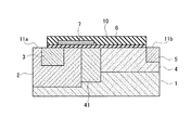
図1Aは、本発明の第1実施形態に係る半導体装置の構成を示す断面図である。本実施形態では半導体装置の一例として、金属酸化膜半導体電界効果トランジスタ(MOSFET)について説明する。
次に、第1実施形態に係る半導体装置101の製造方法について説明する。初めに、ノンドープの炭化珪素絶縁半導体基板(基板1)の第1主面にN型不純物をイオン注入して、第1ドリフト領域4を形成する。その結果、図1Bに示すように、基板1の上面にN−型炭化珪素となる第1ドリフト領域4が形成される。N型不純物としては、窒素を用いることができる。注入濃度は1×10¹⁴〜1×10¹⁸/cm3である。第1ドリフト領域4の厚さは、イオン注入のエネルギーによって調整することができる。本実施形態では、厚さを数μm以下とする。
次に、図1Aに示した第1実施形態に係る半導体装置101の動作について説明する。半導体装置101は、ソース電極15の電圧を基準として、ドレイン電極16に正の電圧を印加した状態でゲート電極7の電圧を制御することで、トランジスタとして機能する。
次に、第1実施形態の変形例について説明する。変形例では、第2ドリフト領域41の不純物濃度を第1ドリフト領域4の不純物濃度よりも低くする。それ以外の構成は、図1Aに示した第1実施形態と同様である。製造方法についても、上述した第1実施形態と同様である。
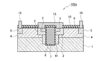
次に、本発明の第2実施形態について説明する。図2Aは、第2実施形態に係る半導体装置の構造を示す断面図である。
次に、第2実施形態に係る半導体装置102の製造方法について説明する。初めに、ノンドープの炭化珪素半導体基板(基板1)上に、マスク材(図示省略)を形成する。マスク材としてはシリコン酸化膜を用いることができ、堆積方法としては熱CVD法やプラズマCVD法を用いることができる。
その後、ゲート溝8の内面にゲート絶縁膜6を形成する。ゲート絶縁膜6を形成する方法として熱酸化法、或いは堆積法を用いることができる。熱酸化法の一例として、酸素雰囲気中に基板1を設置し、温度を1100℃程度に加熱する。基板1が酸素に触れる全ての部分にシリコン酸化膜を形成することができる。ゲート絶縁膜6の形成後、ウェル領域2とゲート絶縁膜6との界面の界面準位を低減するために、窒素、アルゴン、N2O等の雰囲気中で1000℃程度のアニールを行う。
図2Aに示した第2実施形態に係る半導体装置102の基本的な動作について説明する。図2に示す半導体装置102は、ソース電極15の電圧を基準として、ドレイン電極16に正の電圧を印加した状態でゲート電極7の電圧を制御することで、トランジスタとして機能する。
また、基板1にイオン注入することによって、第1ドリフト領域4、第2ドリフト領域41を形成するので、エピ成長が不要になり製造コストを低減することができる。
次に、第2実施形態に係る半導体装置の第1変形例について説明する。装置構成は、図2Aに示した第2実施形態と同様である。第1変形例は、第2ドリフト領域41の不純物濃度が第1ドリフト領域4の不純物濃度より低くする。それ以外は、前述した第2実施形態と同様である。製造方法は、第2実施形態で示した方法と同様である。
オフ状態の電流遮断時には、ドレイン電極16の電圧が上昇するにつれて、ゲート電極7から第2ドリフト領域41、及び第1ドリフト領域4に空乏層が広がり、ドレイン電極16からウェル領域2に電界が生じる。第2ドリフト領域41の不純物濃度が第1ドリフト領域4の不純物濃度よりも低いことにより、ゲート電極7に生じる電界を低減することができる。即ち、耐圧を向上することができ、且つ、抵抗を低減することができる。
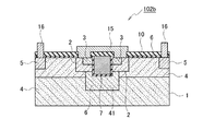
次に、第2実施形態の第2変形例について説明する。図2Hは、第2変形例に係る半導体装置の構成を示す断面図である。図2Hに示す半導体装置102aは、ゲート溝8が第2ドリフト領域41よりも深く形成され、絶縁基板に達している点で、前述した図2Aに示した半導体装置102と相違する。
次に、第2実施形態の第3変形例について説明する。図2Iは、第3変形例に係る半導体装置の構成を示す断面図である。図2Iに示す半導体装置102bは、ゲート溝8が第1ドリフト領域4よりも浅く形成されている点で、前述した図2Aに示した半導体装置102と相違する。
次に、本発明の第3実施形態について説明する。図3Aは、第3実施形態に係る半導体装置の構成を示す断面図である。
図3Aに示すように、第3実施形態に係る半導体装置103は、N型の導電性半導体基板(基板1)の第1主面に形成された、N型の第1ドリフト領域4、及びN型の第2ドリフト領域41を備える。前述した第1、第2実施形態と同様に、第1ドリフト領域4と第2ドリフト領域41は接しており、第1ドリフト領域4よりも第2ドリフト領域41の方が深く形成されている。
次に、第3実施形態に係る半導体装置103の製造方法について説明する。初めに、炭化珪素半導体基板(基板1)上に、イオン注入によってP型のウェル領域2、N+型のソース領域3を形成する。ウェル領域2及びソース領域3を形成後の断面構造を図3Bに示す。ソース領域3とドレイン領域5は不純物濃度が1×10¹⁸/cm3〜1×1021/cm3であるのが好ましい。また、ウェル領域2の濃度は、1×1015/cm3〜1×10 19/cm3であるのが好ましい。
次に、第3実施形態に係る半導体装置103の動作について説明する。図3Aに示す構成の半導体装置103は、ソース電極15の電圧を基準として、ドレイン電極16に正の電圧を印加した状態でゲート電極7の電圧を制御することで、トランジスタとして機能する。即ち、ゲート電極7とソース電極15間の電圧を所定の閾値電圧以上にすると、ゲート電極7の側面に接するウェル領域2のチャンネルに反転層が形成されて、オン状態となる。ドレイン電極16からソース電極15へ電流が流れる。
また、基板1にイオン注入することによって、第1ドリフト領域4、第2ドリフト領域41を形成するので、エピ成長が不要になり製造コストを低減することができる。
次に、第3実施形態の変形例について説明する。変形例では、第2ドリフト領域41の不純物濃度を第1ドリフト領域4の不純物濃度よりも低くする点で相違する。それ以外の構成は、図3Aに示した第3実施形態と同様である。
製造方法は、第3実施形態と対比して、ウェル領域2、ソース領域3、及びドレイン領域5を形成した後に、第1ドリフト領域4と第2ドリフト領域41をイオン注入によって形成し、第2ドリフト領域41にゲート溝8を形成する点で相違する。
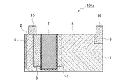
次に、本発明の第4実施形態について説明する。図4Aは、第4実施形態に係る半導体装置の構成を示す斜視図、図4Bは、図4AにおけるX−X´断面図である。
図4A、図4Bに示すように、第4実施形態に係る半導体装置104は、絶縁性半導体からなる基板1を備える。基板1の第1主面には、N型の第1ドリフト領域4が形成され、更に、第1ドリフト領域4と接してP型のウェル領域2が形成されている。ウェル領域2は、第1ドリフト領域4よりも深くまで形成されている。
また、ゲート溝8の側面にてゲート絶縁膜6とウェル領域2が接しているので、ゲート溝8の深さが深いほど、ゲート絶縁膜6とウェル領域2が接する面積が大きくなる。
次に、第4実施形態に係る半導体装置104の製造方法について説明する。初めに、ノンドープの炭化珪素絶縁半導体基板1上に、マスク材(図示省略)を形成し、ゲート溝8に合わせてパターニングする。マスク材としてはシリコン酸化膜を用いることができ、堆積方法としては熱CVD法やプラズマCVD法を用いることができる。パターニングの方法としては、一般的なフォトリソグラフィー法を用いることができる。
その後、ゲート溝8の内面及び基板1の第1主面にゲート絶縁膜6を形成する。ゲート絶縁膜6を形成する方法として熱酸化法、或いは堆積法を用いることができる。熱酸化法の一例として、酸素雰囲気中に基板1を設置し、温度を1100℃程度に加熱する。基板1が酸素に触れる全ての部分にシリコン酸化膜を形成することができる。ゲート絶縁膜6の形成後、ウェル領域2とゲート絶縁膜6との界面の界面準位を低減するために、窒素、アルゴン、N2O等の雰囲気中で1000℃程度のアニールを行う。
また、熱酸化法の他の例として、直接にNO(一酸化窒素)、或いはN2O(一酸化二窒素)の雰囲気中で熱酸化することも可能である。その場合の温度は1100℃〜1400℃とするのが好ましい。形成されるゲート絶縁膜6の厚さは数十nmとするのが好ましい。
コンタクトホールを形成した後に、図4Aに示したように、ウェル領域2及びソース領域3の表面にソース電極15を形成し、更に、ドレイン領域5にドレイン電極16を形成する。電極材料としてはメタルが一般的である。メタルとして、チタン(Ti)、ニッケル(Ni)、或いはモリブデン(Mo)を用いることができる。また、Ti/Ni/Ag等の積層メタルでもよい。ここではチタン(Ti)を用いる例について説明する。初めに、スパッタ法等の堆積方法を用いて、チタン(Ti)を堆積する。次いで、堆積したチタンに対し、レジストマスクによる選択エッチングを行う。その結果、図4Aに示した第4実施形態の半導体装置104が完成する。
次に、図4Aに示した第4実施形態に係る半導体装置104の動作について説明する。図4Aに示す半導体装置104は、ソース電極15の電圧を基準として、ドレイン電極16に正の電圧を印加した状態でゲート電極7の電圧を制御することで、トランジスタとして機能する。
具体的には、電子は、ソース電極15からソース領域3に流れる。更に、一部の電子は、ソース領域3からチャンネルを介して第2ドリフト領域41に流れ、ドレイン領域5へ流れる。残りの電子は、第1ドリフト領域4に流れ、第1ドリフト領域4からドレイン領域5へ流れる。双方の電子は、ドレイン電極16に流れる。
次に、第4実施形態の第1変形例について説明する。第1変形例では、第2ドリフト領域41の不純物濃度を第1ドリフト領域4の不純物濃度よりも低くする点で相違する。それ以外の構成は、図4Aに示した第4実施形態と同様である。
以下、製造方法の相違点について説明する。第1変形例では、ウェル領域2、ソース領域3、及びドレイン領域5を形成した後に、第1ドリフト領域4及び第2ドリフト領域41をイオン注入によって形成する。その後、第2ドリフト領域41にゲート溝8を形成する。それ以外の製造方法は、第4実施形態と同様である。
次に、第4実施形態に係る半導体装置の第2変形例について説明する。図4Gは、第2変形例に係る半導体装置の断面図である。図4Aに示した半導体装置104と対比して、ゲート溝8が第2ドリフト領域41よりも深くまで形成され、絶縁基板に接している点で相違する。
製造方法は、図4Aに示した半導体装置104と対比して、第1ドリフト領域4、及び第2ドリフト領域41を形成する際の、不純物の斜め注入の角度が相違する。具体的には、図4Gに示す半導体装置104aの場合には、ゲート溝8の底部に不純物が注入されないように角度を設定する。例えば、ゲート溝の幅が1μm、深さが1μmの場合には、注入角度を45度以上に設定するのが好ましい。
次に、第4実施形態に係る半導体装置の第3変形例について説明する。装置構成は、図4Aと同様である。相違点は、ソース電極15、ゲート電極7、及びドレイン電極16が、全て同一電圧のときには、第2ドリフト領域41が完全空乏化されることである。例えば、第2ドリフト領域41の濃度が1×10¹⁴/cm3で、ゲート電極7から第2ドリフト領域41までの距離が0.1μm程度であれば、ゲート電極7と第2ドリフト領域41の仕事関数の差によって生じるエネルギーバンドの曲りに起因して、第2ドリフト領域41が完全空乏化される。即ち、第1ドリフト領域4よりも深い領域にて、第2ドリフト領域41とゲート電極7がゲート絶縁膜6を介して生じる静電容量はほぼ皆無となる。その結果、ゲート・ドレイン間の静電容量(Cgd)を低減することができ、高速動作を可能とし、スイッチング損失を低減することができる。
次に、第4実施形態に係る半導体装置の第4変形例について説明する。図4Hは、第4変形例に係る半導体装置の断面図である。図4Hに示すように、第4変形例に係る半導体装置104bは、ドレイン領域5を、ソース領域3と同一の深さに形成している点で、図4Aに示した第4実施形態と相違する。
このような構成とすることにより、ドレイン領域5とソース領域3を同時にイオン注入で形成することができ、製造工程を簡素化し、製造コストを低減することができる。
次に、第4実施形態に係る半導体装置の第5変形例について説明する。図4Iは、第5変形例に係る半導体装置の断面図である。第5変形例に係る半導体装置104cは、図4Aに示した半導体装置104と対比して、基板1の表面から深い位置でソース領域3の幅が狭く、基板1の表面付近でソース領域3の幅が広く形成されている点で相違する。
次に、第4実施形態に係る半導体装置の第6変形例について説明する。図4Jは、第6変形例に係る半導体装置の斜視図である。第6変形例に係る半導体装置104dは、前述した図4Aに示した半導体装置104と対比して、装置全体の周囲が絶縁基板とされている点である。また、製造方法は、第4実施形態と対比して、第1ドリフト領域4を形成するためにマスクを使用して選択的にイオン注入を行う点で相違する。
次に、第4実施形態に係る半導体装置の第7変形例について説明する。図4Kは、第7変形例に係る半導体装置の斜視図である。
第7変形例に係る半導体装置104eは、前述した図4Aに示した半導体装置104と対比して、装置全体の周囲が絶縁基板とされている点、及び、隣接する半導体装置がゲート溝、及びゲート電極7を共有している点である。製造方法は、第4実施形態と同様である。
次に、第4実施形態に係る半導体装置の第8変形例について説明する。図4Lは、第8変形例に係る半導体装置の斜視図である。図4Lに示すように、第8変形例に係る半導体装置104fは、図4Aに示した半導体装置104と対比して、ゲート溝8に対して直交する方向に、ゲート溝8と同一の深さのソース溝17が形成されている点で相違する。更に、ソース溝17の内部に、ウェル領域2、ソース領域3、及びソース電極15が形成されている。ソース溝17は、真上から見たとき、ゲート溝8と直交する方向に形成されている。ソース溝17の側壁は、ソース領域3と接し、ソース溝17の底部はウェル領域2と接している。
次に、第4実施形態に係る半導体装置の第9変形例について説明する。図4Mは、第9変形例に係る半導体装置の斜視図である。図4Mに示すように、第9変形例に係る半導体装置104gは、前述した図4Aに示した半導体装置104と対比して、装置全体の周囲が絶縁基板とされている点で相違する。更に、第9変形例では、ゲート溝8(図4B等を参照)の深さを、半導体装置の繰り返しピッチP1の1/2以上としている点で相違する。
次に、第4実施形態に係る半導体装置の第10変形例について説明する。第10変形例では、図4Aに示した第4実施形態と対比して、第1ドリフト領域4の表面近傍の不純物濃度を低くした点で相違する。製造方法は、イオンを注入して第1ドリフト領域4を形成する際に、低エネルギーのときには、高エネルギーのときよりもドーズ量を低くすればよい。
次に、本発明の第5実施形態について説明する。図5Aは、第5実施形態に係る半導体装置の構成を示す斜視図、図5Bは、図5Aに示すX−X´断面図である。図5A、図5Bでは、煩雑さを避けるため、層間絶縁膜、及びコンタクトホールの記載を省略している。
次に、第5実施形態に係る半導体装置105の製造方法について説明する。まず、ノンドープの炭化珪素絶縁半導体基板(基板1)上にゲート溝8を形成する。ゲート溝8を形成するため、基板1の第1主面にマスク材(図示省略)を堆積し、その後パターニングする。マスク材としてはシリコン酸化膜を用いることができ、堆積方法としては熱CVD法やプラズマCVD法を用いることができる。パターニングの方法としては、一般的なフォトリソグラフィー法を用いることができる。パターニングされたレジストをマスクとして、マスク材をエッチングする。
その後、マスク材上にレジストをパターニングする。
P型不純物としては、アルミやボロンを用いることができる。N型不純物としては、窒素を用いることができる。この際、基体温度を600℃程度に加熱した状態でイオン注入することで、注入領域に結晶欠陥が生じることを抑制することができる。イオンを注入した後、マスク材を、例えばフッ酸を用いたエッチングによって除去する。
層間絶縁膜の堆積後に、コンタクトホール(図示省略)を形成する。層間絶縁膜上にレジスト(図示省略)をパターニングする。パターニングの方法としては、一般的なフォトリソグラフィー法を用いることができる。パターニングされたレジストをマスクにして、層間絶縁膜をエッチングする。エッチング方法としては、フッ酸を用いたウエットエッチングや、反応性イオンエッチングなどのドライエッチングを用いることができる。
コンタクトホールを形成した後、ソース電極(図示省略)、ドレイン電極(図示省略)を形成する。電極材料としてはメタルが一般的である。メタルとしてTi、Ni、Mo等を用いることができる。また、Ti/Ni/Ag等の積層メタルを用いてもよい。ここではチタン(Ti)を用いる例について説明する。初めに、スパッタ法等の堆積方法を用いて、チタン(Ti)を堆積する。次いで、堆積したチタンに対し、レジストマスクによる選択エッチングを行う。その結果、図5Aに示した第5実施形態に係る半導体装置105が完成する。
次に、第5実施形態に係る半導体装置105の動作について説明する。図5Aに示す半導体装置105は、ソース電極15の電圧を基準として、ドレイン電極16に正の電圧を印加した状態でゲート電極7の電圧を制御することで、トランジスタとして機能する。
具体的には、電子は、ソース電極15からソース領域3に流れ、更に、ソース領域3からチャンネルを介して、第2ドリフト領域41に流れ込む。次に、第1ドリフト領域4、第1ドリフト領域4からドレイン領域5を経由してドレイン電極に流れる。即ち、ドレイン電極からソース電極に電流が流れる。
このとき、本実施形態の半導体装置105では、第1ドリフト領域4とコラム領域21のPN接合部から空乏層が伸びる。ドレイン電極16に所定の電圧が印加されると、第1ドリフト領域4とコラム領域21が完全空乏化される。
そして、第1ドリフト領域4とコラム領域21を完全空乏化させるためには、一般的に下記(1)式を満たす必要がある。
Na×Wp=Nd×Wn …(1)
ドナー濃度Ndは半導体装置のオン抵抗に影響し、Ndが大きい方がオン抵抗が小さい。(1)式を維持しながら、オン抵抗を低減するためには、Ndを大きく、Wnを小さくする必要がある。例えば、第1ドリフト領域4とコラム領域21の濃度は双方共に、2×10¹⁷/cm3で、第1ドリフト領域4の厚さは4μmで、コラム領域21の間隔とコラム領域21の幅が1μmである場合、耐圧700V台で、第1ドリフト領域4の抵抗は数十μΩ・cm2となる。
即ち、ドレイン電極16に所定の電圧を印加したときに、コラム領域21、及び第1ドリフト領域4が完全空乏化されることになる。従って、本実施形態に係る半導体装置105では、低いオン抵抗を実現できる。
例えば、上記した各実施形態では、基板1として炭化珪素基板を用いる例について説明したが、本発明は、炭化珪素基板に限らず、GaN,ダイヤモンド、ZnO、AlGaN等のバンドギャップの広い半導体材料の基板を用いることが可能である。
また、上記した各実施形態では、ゲート絶縁膜としてシリコンの酸化膜を用いる例について説明したが、シリコン窒化膜を用いることもできる。更に、シリコン酸化膜とシリコン窒化膜を積層した膜を用いてもよい。
2 ウェル領域
3 ソース領域
4 第1ドリフト領域
5 ドレイン領域
6 ゲート絶縁膜
7 ゲート電極
8 ゲート溝
9 マスク材
10 層間絶縁膜
11a コンタクトホール
11b コンタクトホール
15 ソース電極
16 ドレイン電極
17 ソース溝
21 コラム領域
41 第2ドリフト領域
101 半導体装置
102 半導体装置
102a 半導体装置
102b 半導体装置
103 半導体装置
104 半導体装置
104a 半導体装置
104b 半導体装置
104c 半導体装置
104d 半導体装置
104e 半導体装置
104f 半導体装置
104g 半導体装置
105 半導体装置
Claims (16)
- 基板と、
前記基板の第1主面に形成された第1導電型の第1ドリフト領域と、
前記基板の第1主面に形成され、前記第1ドリフト領域と接し、且つ、前記第1ドリフト領域よりも前記基板の深い位置まで形成され、前記第1ドリフト領域と同一の不純物濃度である第1導電型の第2ドリフト領域と、
前記基板の第1主面に形成され、前記第2ドリフト領域に接する第2導電型のウェル領域と、
前記ウェル領域内にて、該ウェル領域の表面から垂直方向に延設された第1導電型のソース領域と、
前記第1ドリフト領域内にて、前記ウェル領域と離間して、第1ドリフト領域の表面から垂直方向に延設された第1導電型のドレイン領域と、
前記第2ドリフト領域、前記ウェル領域、前記ソース領域に接して形成されたゲート絶縁膜と、
前記ゲート絶縁膜に接し、前記ゲート絶縁膜を介して前記第2ドリフト領域、前記ウェル領域、前記ソース領域に接するように形成されたゲート電極と、
前記ソース領域、及び前記ウェル領域に接続されたソース電極と、
前記ドレイン領域に接続されたドレイン電極と、
を備えたことを特徴とする半導体装置。 - 請求項1に記載の半導体装置において、
前記基板は、半絶縁性基板、或いは絶縁基板であること
を特徴とする半導体装置。 - 請求項1、3のいずれかに記載の半導体装置において、
前記基板は、ワイドバンドギャップ半導体であること
を特徴とする半導体装置。 - 請求項1、3、4のいずれか1項に記載の半導体装置において、
前記第2ドリフト領域に接して形成されるゲート溝を有し、前記ゲート絶縁膜及び前記ゲート電極は、前記ゲート溝の内面に形成されること
を特徴とする記載の半導体装置。 - 請求項5に記載の半導体装置において、
前記ゲート絶縁膜と前記ウェル領域が接する面積は、前記ゲート溝の深さが深いほど大きくなること
を特徴とする半導体装置。 - 請求項5または6に記載の半導体装置において、
前記ゲート溝は、前記第2ドリフト領域よりも深くまで形成されること
を特徴とする半導体装置。 - 請求項5〜7のいずれか1項に記載の半導体装置において、
前記ウェル領域は、前記ゲート溝より深いこと
を特徴とする半導体装置。 - 請求項1、3〜8のいずれか1項に記載の半導体装置において、
前記ゲート電極、前記ソース電極、及び前記ドレイン電極は、全てが同一電圧のとき、前記第2ドリフト領域が完全空乏化されること
を特徴とする半導体装置。 - 請求項1、3〜9のいずれか1項に記載の半導体装置において、
前記第1ドリフト領域は、表面近傍の不純物濃度が低いこと
を特徴とする半導体装置。 - 請求項5〜8のいずれか1項に記載の半導体装置において、
一部が前記第1ドリフト領域内にて、該第1ドリフト領域よりも浅い位置まで形成され、他の一部が前記ゲート溝の底部まで形成されて前記ソース領域と接する第2導電型のコラム領域を更に備え、
前記コラム領域は、前記ソース電極と同電位であること
を特徴とする半導体装置。 - 請求項11に記載の半導体装置において、
前記コラム領域は、前記ゲート絶縁膜の、前記ドレイン電極と対向する面の少なくとも一部に接すること
を特徴とする半導体装置。 - 請求項11または12に記載の半導体装置において、
前記ドレイン電極に所定の電圧を印加したときに、前記コラム領域、及び前記第1ドリフト領域は完全空乏化されること
を特徴とする半導体装置。 - 基板と、
前記基板の第1主面に形成された第1導電型の第1ドリフト領域と、
前記基板の第1主面に形成され、前記第1ドリフト領域と接し、且つ、前記第1ドリフト領域よりも前記基板の深い位置まで形成され、前記第1ドリフト領域と同一の不純物濃度である第1導電型の第2ドリフト領域と、
前記基板の第1主面に形成され、前記第2ドリフト領域に接する第2導電型のウェル領域と、
前記ウェル領域内にて、該ウェル領域の表面から垂直方向に延設された第1導電型のソース領域と、
前記第1ドリフト領域内にて、前記ウェル領域と離間して、第1ドリフト領域の表面から垂直方向に延設された第1導電型のドレイン領域と、
前記第2ドリフト領域、前記ウェル領域、前記ソース領域に接して形成されたゲート絶縁膜と、
前記ゲート絶縁膜に接し、前記ゲート絶縁膜を介して前記第2ドリフト領域、前記ウェル領域、前記ソース領域に接するように形成されたゲート電極と、
前記ソース領域、及び前記ウェル領域に接続されたソース電極と、
前記ドレイン領域に接続されたドレイン電極と、
を備えた半導体装置を製造する半導体装置の製造方法であって、
前記第1ドリフト領域、及び前記第2ドリフト領域を、不純物の注入及び活性化で形成すること
を特徴とする半導体装置の製造方法。 - 請求項14記載の半導体装置の製造方法において、
前記不純物の注入は、イオン注入法を用いること
を特徴とする半導体装置の製造方法。 - 請求項14または15に記載の半導体装置の製造方法において、
前記第1ドリフト領域と、前記第2ドリフト領域を同時に形成すること
を特徴とする半導体装置の製造方法。 - 基板と、
前記基板の第1主面に形成された第1導電型の第1ドリフト領域と、
前記基板の第1主面に形成され、前記第1ドリフト領域と接し、且つ、前記第1ドリフト領域よりも前記基板の深い位置まで形成された第1導電型の第2ドリフト領域と、
前記基板の第1主面に形成され、前記第2ドリフト領域に接する第2導電型のウェル領域と、
前記ウェル領域内にて、該ウェル領域の表面から垂直方向に延設された第1導電型のソース領域と、
前記第1ドリフト領域内にて、前記ウェル領域と離間して、第1ドリフト領域の表面から垂直方向に延設された第1導電型のドレイン領域と、
前記第2ドリフト領域、前記ウェル領域、前記ソース領域に接して形成されたゲート絶縁膜と、
前記ゲート絶縁膜に接し、前記ゲート絶縁膜を介して前記第2ドリフト領域、前記ウェル領域、前記ソース領域に接するように形成されたゲート電極と、
前記ソース領域、及び前記ウェル領域に接続されたソース電極と、
前記ドレイン領域に接続されたドレイン電極と、
前記第2ドリフト領域に形成されるゲート溝と、
を備えた半導体装置の製造方法であって、
前記ゲート溝を形成した後に、前記第2ドリフト領域を形成すること
を特徴とする半導体装置の製造方法。
Applications Claiming Priority (1)
| Application Number | Priority Date | Filing Date | Title |
|---|---|---|---|
| PCT/JP2017/005333 WO2018150467A1 (ja) | 2017-02-14 | 2017-02-14 | 半導体装置および半導体装置の製造方法 |
Publications (2)
| Publication Number | Publication Date |
|---|---|
| JPWO2018150467A1 JPWO2018150467A1 (ja) | 2019-12-12 |
| JP6725055B2 true JP6725055B2 (ja) | 2020-07-15 |
Family
ID=63170568
Family Applications (1)
| Application Number | Title | Priority Date | Filing Date |
|---|---|---|---|
| JP2019500070A Active JP6725055B2 (ja) | 2017-02-14 | 2017-02-14 | 半導体装置および半導体装置の製造方法 |
Country Status (11)
| Country | Link |
|---|---|
| US (1) | US20200020775A1 (ja) |
| EP (1) | EP3584824A4 (ja) |
| JP (1) | JP6725055B2 (ja) |
| KR (1) | KR102056037B1 (ja) |
| CN (1) | CN110291620B (ja) |
| BR (1) | BR112019016822A2 (ja) |
| CA (1) | CA3053635C (ja) |
| MX (1) | MX2019009532A (ja) |
| MY (1) | MY186880A (ja) |
| RU (1) | RU2719569C1 (ja) |
| WO (1) | WO2018150467A1 (ja) |
Families Citing this family (6)
| Publication number | Priority date | Publication date | Assignee | Title |
|---|---|---|---|---|
| JP6962457B2 (ja) * | 2018-04-19 | 2021-11-05 | 日産自動車株式会社 | 半導体装置及び半導体装置の製造方法 |
| JP7354029B2 (ja) * | 2020-03-13 | 2023-10-02 | 株式会社東芝 | 半導体装置、半導体装置の製造方法、電源回路、及び、コンピュータ |
| US11894457B2 (en) * | 2020-05-09 | 2024-02-06 | Joulwatt Technology Co., Ltd. | Semiconductor device and manufacturing method thereof |
| CN114078707A (zh) * | 2020-08-21 | 2022-02-22 | 中芯国际集成电路制造(上海)有限公司 | 半导体结构及其形成方法 |
| JPWO2022118055A1 (ja) | 2020-12-01 | 2022-06-09 | ||
| CN113394291A (zh) * | 2021-04-29 | 2021-09-14 | 电子科技大学 | 横向功率半导体器件 |
Family Cites Families (23)
| Publication number | Priority date | Publication date | Assignee | Title |
|---|---|---|---|---|
| JPH0418762A (ja) * | 1990-05-14 | 1992-01-22 | Hitachi Ltd | 絶縁ゲート形電界効果トランジスタ |
| KR100553650B1 (ko) | 1997-06-23 | 2006-02-24 | 제임스 알버트 주니어 쿠퍼 | 폭이 넓은 밴드갭 반도체 내의 전력 소자 |
| JP3405681B2 (ja) * | 1997-07-31 | 2003-05-12 | 株式会社東芝 | 半導体装置 |
| JP4653704B2 (ja) | 1999-05-21 | 2011-03-16 | 関西電力株式会社 | 半導体装置 |
| KR100445904B1 (ko) * | 2001-12-12 | 2004-08-25 | 한국전자통신연구원 | 소스 필드 플레이트를 갖는 드레인 확장형 모스 전계 효과트랜지스터 및그 제조방법 |
| JP4677166B2 (ja) * | 2002-06-27 | 2011-04-27 | 三洋電機株式会社 | 半導体装置及びその製造方法 |
| JP3941641B2 (ja) * | 2002-09-18 | 2007-07-04 | 日産自動車株式会社 | 炭化珪素半導体装置の製造方法とその製造方法によって製造される炭化珪素半導体装置 |
| US7033891B2 (en) * | 2002-10-03 | 2006-04-25 | Fairchild Semiconductor Corporation | Trench gate laterally diffused MOSFET devices and methods for making such devices |
| JP4225177B2 (ja) * | 2002-12-18 | 2009-02-18 | 株式会社デンソー | 半導体装置およびその製造方法 |
| US7238986B2 (en) * | 2004-05-03 | 2007-07-03 | Texas Instruments Incorporated | Robust DEMOS transistors and method for making the same |
| JP2008210994A (ja) * | 2007-02-27 | 2008-09-11 | Nec Electronics Corp | 横型mosfetおよびその製造方法 |
| JP5420854B2 (ja) * | 2008-04-28 | 2014-02-19 | パナソニック株式会社 | 半導体装置およびその製造方法 |
| US7888734B2 (en) * | 2008-12-04 | 2011-02-15 | Taiwan Semiconductor Manufacturing Company, Ltd. | High-voltage MOS devices having gates extending into recesses of substrates |
| WO2011135995A1 (ja) * | 2010-04-26 | 2011-11-03 | 三菱電機株式会社 | 半導体装置 |
| WO2012144271A1 (ja) * | 2011-04-19 | 2012-10-26 | 日産自動車株式会社 | 半導体装置およびその製造方法 |
| KR101279256B1 (ko) * | 2011-08-31 | 2013-06-26 | 주식회사 케이이씨 | 전력 반도체 소자 |
| KR101867953B1 (ko) * | 2011-12-22 | 2018-06-18 | 삼성전자주식회사 | 반도체 소자 및 반도체 소자의 형성 방법 |
| US9136158B2 (en) * | 2012-03-09 | 2015-09-15 | Taiwan Semiconductor Manufacturing Company, Ltd. | Lateral MOSFET with dielectric isolation trench |
| KR101872942B1 (ko) * | 2012-03-29 | 2018-06-29 | 삼성전자주식회사 | 반도체 장치 |
| KR101671651B1 (ko) * | 2012-10-16 | 2016-11-16 | 아사히 가세이 일렉트로닉스 가부시끼가이샤 | 전계 효과 트랜지스터 및 반도체 장치 |
| US9142668B2 (en) * | 2013-03-13 | 2015-09-22 | Cree, Inc. | Field effect transistor devices with buried well protection regions |
| US10861938B2 (en) * | 2013-07-19 | 2020-12-08 | Nissan Motor Co., Ltd. | Semiconductor device and method of manufacturing the same |
| CN104518027B (zh) * | 2014-06-13 | 2019-06-11 | 上海华虹宏力半导体制造有限公司 | Ldmos器件及其制造方法 |
-
2017
- 2017-02-14 CA CA3053635A patent/CA3053635C/en active Active
- 2017-02-14 CN CN201780086361.4A patent/CN110291620B/zh active Active
- 2017-02-14 MX MX2019009532A patent/MX2019009532A/es unknown
- 2017-02-14 MY MYPI2019004603A patent/MY186880A/en unknown
- 2017-02-14 BR BR112019016822A patent/BR112019016822A2/pt not_active Application Discontinuation
- 2017-02-14 US US16/485,496 patent/US20200020775A1/en not_active Abandoned
- 2017-02-14 KR KR1020197025826A patent/KR102056037B1/ko active IP Right Grant
- 2017-02-14 EP EP17896530.7A patent/EP3584824A4/en not_active Withdrawn
- 2017-02-14 WO PCT/JP2017/005333 patent/WO2018150467A1/ja unknown
- 2017-02-14 RU RU2019128853A patent/RU2719569C1/ru active
- 2017-02-14 JP JP2019500070A patent/JP6725055B2/ja active Active
Also Published As
| Publication number | Publication date |
|---|---|
| BR112019016822A2 (pt) | 2020-04-07 |
| MY186880A (en) | 2021-08-26 |
| KR102056037B1 (ko) | 2019-12-13 |
| KR20190112798A (ko) | 2019-10-07 |
| CN110291620A (zh) | 2019-09-27 |
| RU2719569C1 (ru) | 2020-04-21 |
| WO2018150467A1 (ja) | 2018-08-23 |
| JPWO2018150467A1 (ja) | 2019-12-12 |
| MX2019009532A (es) | 2019-09-16 |
| EP3584824A1 (en) | 2019-12-25 |
| CA3053635A1 (en) | 2018-08-23 |
| CA3053635C (en) | 2020-08-18 |
| EP3584824A4 (en) | 2020-08-05 |
| CN110291620B (zh) | 2020-07-14 |
| US20200020775A1 (en) | 2020-01-16 |
Similar Documents
| Publication | Publication Date | Title |
|---|---|---|
| JP6725055B2 (ja) | 半導体装置および半導体装置の製造方法 | |
| JP5433352B2 (ja) | 半導体装置の製造方法 | |
| JP6109444B1 (ja) | 半導体装置 | |
| JP6038391B2 (ja) | 半導体装置 | |
| JP2012169385A (ja) | 炭化珪素半導体装置 | |
| US10651270B2 (en) | Semiconductor device having a trench structure | |
| JP7006280B2 (ja) | 半導体装置 | |
| JP6802454B2 (ja) | 半導体装置およびその製造方法 | |
| JP7057555B2 (ja) | 半導体装置 | |
| JP5971218B2 (ja) | 半導体装置 | |
| JP2014127547A (ja) | 半導体装置の製造方法 | |
| JP6870516B2 (ja) | 半導体装置および半導体装置の製造方法 | |
| JPWO2015111218A1 (ja) | 半導体装置 | |
| WO2017010164A1 (ja) | 電力用半導体装置 | |
| JP7092188B2 (ja) | 半導体装置及びその製造方法 | |
| JP6969684B2 (ja) | 半導体装置及びその製造方法 | |
| JPWO2017208301A1 (ja) | 半導体装置 | |
| JP6950816B2 (ja) | 半導体装置及びその製造方法 | |
| JP2019096776A (ja) | 半導体装置及びその製造方法 | |
| JP7257423B2 (ja) | 半導体装置及びその製造方法 | |
| JP2020205309A (ja) | 半導体装置及びその製造方法 | |
| JP2015057851A (ja) | 半導体装置 |
Legal Events
| Date | Code | Title | Description |
|---|---|---|---|
| A529 | Written submission of copy of amendment under article 34 pct |
Free format text: JAPANESE INTERMEDIATE CODE: A5211 Effective date: 20190805 |
|
| A521 | Request for written amendment filed |
Free format text: JAPANESE INTERMEDIATE CODE: A523 Effective date: 20190827 |
|
| A621 | Written request for application examination |
Free format text: JAPANESE INTERMEDIATE CODE: A621 Effective date: 20190827 |
|
| TRDD | Decision of grant or rejection written | ||
| A01 | Written decision to grant a patent or to grant a registration (utility model) |
Free format text: JAPANESE INTERMEDIATE CODE: A01 Effective date: 20200526 |
|
| A61 | First payment of annual fees (during grant procedure) |
Free format text: JAPANESE INTERMEDIATE CODE: A61 Effective date: 20200608 |
|
| R151 | Written notification of patent or utility model registration |
Ref document number: 6725055 Country of ref document: JP Free format text: JAPANESE INTERMEDIATE CODE: R151 |