JP6324098B2 - 表示装置及びその製造方法 - Google Patents
表示装置及びその製造方法 Download PDFInfo
- Publication number
- JP6324098B2 JP6324098B2 JP2014021746A JP2014021746A JP6324098B2 JP 6324098 B2 JP6324098 B2 JP 6324098B2 JP 2014021746 A JP2014021746 A JP 2014021746A JP 2014021746 A JP2014021746 A JP 2014021746A JP 6324098 B2 JP6324098 B2 JP 6324098B2
- Authority
- JP
- Japan
- Prior art keywords
- insulating film
- terminal
- film
- display device
- forming
- Prior art date
- Legal status (The legal status is an assumption and is not a legal conclusion. Google has not performed a legal analysis and makes no representation as to the accuracy of the status listed.)
- Active
Links
- 238000004519 manufacturing process Methods 0.000 title claims description 25
- 239000010408 film Substances 0.000 claims description 332
- 239000010409 thin film Substances 0.000 claims description 61
- 239000000758 substrate Substances 0.000 claims description 53
- 238000000034 method Methods 0.000 claims description 18
- 239000004642 Polyimide Substances 0.000 claims description 7
- NIXOWILDQLNWCW-UHFFFAOYSA-N acrylic acid group Chemical group C(C=C)(=O)O NIXOWILDQLNWCW-UHFFFAOYSA-N 0.000 claims description 7
- 229920001721 polyimide Polymers 0.000 claims description 7
- 239000010410 layer Substances 0.000 description 46
- 230000001681 protective effect Effects 0.000 description 13
- 238000007789 sealing Methods 0.000 description 12
- 238000005530 etching Methods 0.000 description 10
- 238000000059 patterning Methods 0.000 description 9
- 229910052581 Si3N4 Inorganic materials 0.000 description 8
- HQVNEWCFYHHQES-UHFFFAOYSA-N silicon nitride Chemical compound N12[Si]34N5[Si]62N3[Si]51N64 HQVNEWCFYHHQES-UHFFFAOYSA-N 0.000 description 8
- 239000011368 organic material Substances 0.000 description 7
- 239000002245 particle Substances 0.000 description 7
- 239000011229 interlayer Substances 0.000 description 6
- 239000004973 liquid crystal related substance Substances 0.000 description 6
- 239000003990 capacitor Substances 0.000 description 5
- 229910052782 aluminium Inorganic materials 0.000 description 4
- XAGFODPZIPBFFR-UHFFFAOYSA-N aluminium Chemical compound [Al] XAGFODPZIPBFFR-UHFFFAOYSA-N 0.000 description 4
- 238000010586 diagram Methods 0.000 description 4
- 229910052751 metal Inorganic materials 0.000 description 4
- 239000002184 metal Substances 0.000 description 4
- 229920005989 resin Polymers 0.000 description 4
- 239000011347 resin Substances 0.000 description 4
- VYPSYNLAJGMNEJ-UHFFFAOYSA-N Silicium dioxide Chemical compound O=[Si]=O VYPSYNLAJGMNEJ-UHFFFAOYSA-N 0.000 description 3
- 230000007547 defect Effects 0.000 description 3
- 230000002542 deteriorative effect Effects 0.000 description 3
- 239000000463 material Substances 0.000 description 3
- 229910021420 polycrystalline silicon Inorganic materials 0.000 description 3
- 229920005591 polysilicon Polymers 0.000 description 3
- 229910052814 silicon oxide Inorganic materials 0.000 description 3
- 239000011248 coating agent Substances 0.000 description 2
- 238000000576 coating method Methods 0.000 description 2
- 230000007797 corrosion Effects 0.000 description 2
- 238000005260 corrosion Methods 0.000 description 2
- 239000011521 glass Substances 0.000 description 2
- 238000002347 injection Methods 0.000 description 2
- 239000007924 injection Substances 0.000 description 2
- 230000002093 peripheral effect Effects 0.000 description 2
- XLYOFNOQVPJJNP-UHFFFAOYSA-N water Substances O XLYOFNOQVPJJNP-UHFFFAOYSA-N 0.000 description 2
- 230000015572 biosynthetic process Effects 0.000 description 1
- 230000006866 deterioration Effects 0.000 description 1
- 238000005401 electroluminescence Methods 0.000 description 1
- 239000003822 epoxy resin Substances 0.000 description 1
- 230000005525 hole transport Effects 0.000 description 1
- 239000012535 impurity Substances 0.000 description 1
- 238000010030 laminating Methods 0.000 description 1
- 239000011159 matrix material Substances 0.000 description 1
- 239000007769 metal material Substances 0.000 description 1
- 238000012986 modification Methods 0.000 description 1
- 230000004048 modification Effects 0.000 description 1
- 239000012044 organic layer Substances 0.000 description 1
- 238000005192 partition Methods 0.000 description 1
- 229920000647 polyepoxide Polymers 0.000 description 1
- 239000000565 sealant Substances 0.000 description 1
- 239000003566 sealing material Substances 0.000 description 1
- 238000000638 solvent extraction Methods 0.000 description 1
- 229920001187 thermosetting polymer Polymers 0.000 description 1
- 239000012780 transparent material Substances 0.000 description 1
Images


Classifications
-
- H—ELECTRICITY
- H01—ELECTRIC ELEMENTS
- H01L—SEMICONDUCTOR DEVICES NOT COVERED BY CLASS H10
- H01L27/00—Devices consisting of a plurality of semiconductor or other solid-state components formed in or on a common substrate
- H01L27/02—Devices consisting of a plurality of semiconductor or other solid-state components formed in or on a common substrate including semiconductor components specially adapted for rectifying, oscillating, amplifying or switching and having at least one potential-jump barrier or surface barrier; including integrated passive circuit elements with at least one potential-jump barrier or surface barrier
- H01L27/12—Devices consisting of a plurality of semiconductor or other solid-state components formed in or on a common substrate including semiconductor components specially adapted for rectifying, oscillating, amplifying or switching and having at least one potential-jump barrier or surface barrier; including integrated passive circuit elements with at least one potential-jump barrier or surface barrier the substrate being other than a semiconductor body, e.g. an insulating body
- H01L27/1214—Devices consisting of a plurality of semiconductor or other solid-state components formed in or on a common substrate including semiconductor components specially adapted for rectifying, oscillating, amplifying or switching and having at least one potential-jump barrier or surface barrier; including integrated passive circuit elements with at least one potential-jump barrier or surface barrier the substrate being other than a semiconductor body, e.g. an insulating body comprising a plurality of TFTs formed on a non-semiconducting substrate, e.g. driving circuits for AMLCDs
- H01L27/124—Devices consisting of a plurality of semiconductor or other solid-state components formed in or on a common substrate including semiconductor components specially adapted for rectifying, oscillating, amplifying or switching and having at least one potential-jump barrier or surface barrier; including integrated passive circuit elements with at least one potential-jump barrier or surface barrier the substrate being other than a semiconductor body, e.g. an insulating body comprising a plurality of TFTs formed on a non-semiconducting substrate, e.g. driving circuits for AMLCDs with a particular composition, shape or layout of the wiring layers specially adapted to the circuit arrangement, e.g. scanning lines in LCD pixel circuits
-
- G—PHYSICS
- G02—OPTICS
- G02F—OPTICAL DEVICES OR ARRANGEMENTS FOR THE CONTROL OF LIGHT BY MODIFICATION OF THE OPTICAL PROPERTIES OF THE MEDIA OF THE ELEMENTS INVOLVED THEREIN; NON-LINEAR OPTICS; FREQUENCY-CHANGING OF LIGHT; OPTICAL LOGIC ELEMENTS; OPTICAL ANALOGUE/DIGITAL CONVERTERS
- G02F1/00—Devices or arrangements for the control of the intensity, colour, phase, polarisation or direction of light arriving from an independent light source, e.g. switching, gating or modulating; Non-linear optics
- G02F1/01—Devices or arrangements for the control of the intensity, colour, phase, polarisation or direction of light arriving from an independent light source, e.g. switching, gating or modulating; Non-linear optics for the control of the intensity, phase, polarisation or colour
- G02F1/13—Devices or arrangements for the control of the intensity, colour, phase, polarisation or direction of light arriving from an independent light source, e.g. switching, gating or modulating; Non-linear optics for the control of the intensity, phase, polarisation or colour based on liquid crystals, e.g. single liquid crystal display cells
- G02F1/133—Constructional arrangements; Operation of liquid crystal cells; Circuit arrangements
- G02F1/136—Liquid crystal cells structurally associated with a semi-conducting layer or substrate, e.g. cells forming part of an integrated circuit
- G02F1/1362—Active matrix addressed cells
- G02F1/1368—Active matrix addressed cells in which the switching element is a three-electrode device
-
- H—ELECTRICITY
- H01—ELECTRIC ELEMENTS
- H01L—SEMICONDUCTOR DEVICES NOT COVERED BY CLASS H10
- H01L27/00—Devices consisting of a plurality of semiconductor or other solid-state components formed in or on a common substrate
- H01L27/02—Devices consisting of a plurality of semiconductor or other solid-state components formed in or on a common substrate including semiconductor components specially adapted for rectifying, oscillating, amplifying or switching and having at least one potential-jump barrier or surface barrier; including integrated passive circuit elements with at least one potential-jump barrier or surface barrier
- H01L27/12—Devices consisting of a plurality of semiconductor or other solid-state components formed in or on a common substrate including semiconductor components specially adapted for rectifying, oscillating, amplifying or switching and having at least one potential-jump barrier or surface barrier; including integrated passive circuit elements with at least one potential-jump barrier or surface barrier the substrate being other than a semiconductor body, e.g. an insulating body
- H01L27/1214—Devices consisting of a plurality of semiconductor or other solid-state components formed in or on a common substrate including semiconductor components specially adapted for rectifying, oscillating, amplifying or switching and having at least one potential-jump barrier or surface barrier; including integrated passive circuit elements with at least one potential-jump barrier or surface barrier the substrate being other than a semiconductor body, e.g. an insulating body comprising a plurality of TFTs formed on a non-semiconducting substrate, e.g. driving circuits for AMLCDs
- H01L27/1222—Devices consisting of a plurality of semiconductor or other solid-state components formed in or on a common substrate including semiconductor components specially adapted for rectifying, oscillating, amplifying or switching and having at least one potential-jump barrier or surface barrier; including integrated passive circuit elements with at least one potential-jump barrier or surface barrier the substrate being other than a semiconductor body, e.g. an insulating body comprising a plurality of TFTs formed on a non-semiconducting substrate, e.g. driving circuits for AMLCDs with a particular composition, shape or crystalline structure of the active layer
-
- H—ELECTRICITY
- H01—ELECTRIC ELEMENTS
- H01L—SEMICONDUCTOR DEVICES NOT COVERED BY CLASS H10
- H01L27/00—Devices consisting of a plurality of semiconductor or other solid-state components formed in or on a common substrate
- H01L27/02—Devices consisting of a plurality of semiconductor or other solid-state components formed in or on a common substrate including semiconductor components specially adapted for rectifying, oscillating, amplifying or switching and having at least one potential-jump barrier or surface barrier; including integrated passive circuit elements with at least one potential-jump barrier or surface barrier
- H01L27/12—Devices consisting of a plurality of semiconductor or other solid-state components formed in or on a common substrate including semiconductor components specially adapted for rectifying, oscillating, amplifying or switching and having at least one potential-jump barrier or surface barrier; including integrated passive circuit elements with at least one potential-jump barrier or surface barrier the substrate being other than a semiconductor body, e.g. an insulating body
- H01L27/1214—Devices consisting of a plurality of semiconductor or other solid-state components formed in or on a common substrate including semiconductor components specially adapted for rectifying, oscillating, amplifying or switching and having at least one potential-jump barrier or surface barrier; including integrated passive circuit elements with at least one potential-jump barrier or surface barrier the substrate being other than a semiconductor body, e.g. an insulating body comprising a plurality of TFTs formed on a non-semiconducting substrate, e.g. driving circuits for AMLCDs
- H01L27/1248—Devices consisting of a plurality of semiconductor or other solid-state components formed in or on a common substrate including semiconductor components specially adapted for rectifying, oscillating, amplifying or switching and having at least one potential-jump barrier or surface barrier; including integrated passive circuit elements with at least one potential-jump barrier or surface barrier the substrate being other than a semiconductor body, e.g. an insulating body comprising a plurality of TFTs formed on a non-semiconducting substrate, e.g. driving circuits for AMLCDs with a particular composition or shape of the interlayer dielectric specially adapted to the circuit arrangement
-
- H—ELECTRICITY
- H01—ELECTRIC ELEMENTS
- H01L—SEMICONDUCTOR DEVICES NOT COVERED BY CLASS H10
- H01L27/00—Devices consisting of a plurality of semiconductor or other solid-state components formed in or on a common substrate
- H01L27/02—Devices consisting of a plurality of semiconductor or other solid-state components formed in or on a common substrate including semiconductor components specially adapted for rectifying, oscillating, amplifying or switching and having at least one potential-jump barrier or surface barrier; including integrated passive circuit elements with at least one potential-jump barrier or surface barrier
- H01L27/12—Devices consisting of a plurality of semiconductor or other solid-state components formed in or on a common substrate including semiconductor components specially adapted for rectifying, oscillating, amplifying or switching and having at least one potential-jump barrier or surface barrier; including integrated passive circuit elements with at least one potential-jump barrier or surface barrier the substrate being other than a semiconductor body, e.g. an insulating body
- H01L27/1214—Devices consisting of a plurality of semiconductor or other solid-state components formed in or on a common substrate including semiconductor components specially adapted for rectifying, oscillating, amplifying or switching and having at least one potential-jump barrier or surface barrier; including integrated passive circuit elements with at least one potential-jump barrier or surface barrier the substrate being other than a semiconductor body, e.g. an insulating body comprising a plurality of TFTs formed on a non-semiconducting substrate, e.g. driving circuits for AMLCDs
- H01L27/1259—Multistep manufacturing methods
- H01L27/1262—Multistep manufacturing methods with a particular formation, treatment or coating of the substrate
-
- H—ELECTRICITY
- H01—ELECTRIC ELEMENTS
- H01L—SEMICONDUCTOR DEVICES NOT COVERED BY CLASS H10
- H01L29/00—Semiconductor devices adapted for rectifying, amplifying, oscillating or switching, or capacitors or resistors with at least one potential-jump barrier or surface barrier, e.g. PN junction depletion layer or carrier concentration layer; Details of semiconductor bodies or of electrodes thereof ; Multistep manufacturing processes therefor
- H01L29/66—Types of semiconductor device ; Multistep manufacturing processes therefor
- H01L29/68—Types of semiconductor device ; Multistep manufacturing processes therefor controllable by only the electric current supplied, or only the electric potential applied, to an electrode which does not carry the current to be rectified, amplified or switched
- H01L29/76—Unipolar devices, e.g. field effect transistors
- H01L29/772—Field effect transistors
- H01L29/78—Field effect transistors with field effect produced by an insulated gate
- H01L29/786—Thin film transistors, i.e. transistors with a channel being at least partly a thin film
- H01L29/78651—Silicon transistors
- H01L29/7866—Non-monocrystalline silicon transistors
- H01L29/78672—Polycrystalline or microcrystalline silicon transistor
- H01L29/78675—Polycrystalline or microcrystalline silicon transistor with normal-type structure, e.g. with top gate
-
- H—ELECTRICITY
- H10—SEMICONDUCTOR DEVICES; ELECTRIC SOLID-STATE DEVICES NOT OTHERWISE PROVIDED FOR
- H10K—ORGANIC ELECTRIC SOLID-STATE DEVICES
- H10K50/00—Organic light-emitting devices
- H10K50/80—Constructional details
- H10K50/84—Passivation; Containers; Encapsulations
- H10K50/844—Encapsulations
-
- H—ELECTRICITY
- H10—SEMICONDUCTOR DEVICES; ELECTRIC SOLID-STATE DEVICES NOT OTHERWISE PROVIDED FOR
- H10K—ORGANIC ELECTRIC SOLID-STATE DEVICES
- H10K59/00—Integrated devices, or assemblies of multiple devices, comprising at least one organic light-emitting element covered by group H10K50/00
- H10K59/10—OLED displays
- H10K59/12—Active-matrix OLED [AMOLED] displays
- H10K59/131—Interconnections, e.g. wiring lines or terminals
-
- H—ELECTRICITY
- H10—SEMICONDUCTOR DEVICES; ELECTRIC SOLID-STATE DEVICES NOT OTHERWISE PROVIDED FOR
- H10K—ORGANIC ELECTRIC SOLID-STATE DEVICES
- H10K59/00—Integrated devices, or assemblies of multiple devices, comprising at least one organic light-emitting element covered by group H10K50/00
- H10K59/80—Constructional details
- H10K59/87—Passivation; Containers; Encapsulations
- H10K59/873—Encapsulations
-
- H—ELECTRICITY
- H10—SEMICONDUCTOR DEVICES; ELECTRIC SOLID-STATE DEVICES NOT OTHERWISE PROVIDED FOR
- H10K—ORGANIC ELECTRIC SOLID-STATE DEVICES
- H10K59/00—Integrated devices, or assemblies of multiple devices, comprising at least one organic light-emitting element covered by group H10K50/00
- H10K59/10—OLED displays
- H10K59/12—Active-matrix OLED [AMOLED] displays
- H10K59/1201—Manufacture or treatment
-
- H—ELECTRICITY
- H10—SEMICONDUCTOR DEVICES; ELECTRIC SOLID-STATE DEVICES NOT OTHERWISE PROVIDED FOR
- H10K—ORGANIC ELECTRIC SOLID-STATE DEVICES
- H10K59/00—Integrated devices, or assemblies of multiple devices, comprising at least one organic light-emitting element covered by group H10K50/00
- H10K59/10—OLED displays
- H10K59/12—Active-matrix OLED [AMOLED] displays
- H10K59/121—Active-matrix OLED [AMOLED] displays characterised by the geometry or disposition of pixel elements
- H10K59/1213—Active-matrix OLED [AMOLED] displays characterised by the geometry or disposition of pixel elements the pixel elements being TFTs
-
- H—ELECTRICITY
- H10—SEMICONDUCTOR DEVICES; ELECTRIC SOLID-STATE DEVICES NOT OTHERWISE PROVIDED FOR
- H10K—ORGANIC ELECTRIC SOLID-STATE DEVICES
- H10K59/00—Integrated devices, or assemblies of multiple devices, comprising at least one organic light-emitting element covered by group H10K50/00
- H10K59/10—OLED displays
- H10K59/12—Active-matrix OLED [AMOLED] displays
- H10K59/122—Pixel-defining structures or layers, e.g. banks
Description
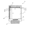
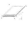
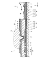
以下、図4乃至図6を参照し、本発明の第1の実施形態に係る表示装置10の概略構成について説明する。図4は、本発明の第1の実施形態に係る表示装置10の概略構成を示す断面図である。図5は、本発明の第1の実施形態に係る表示装置10の端子部の概略構成を示す図であり、(a)は端子部の平面図であり、(b)は端子部の断面図である。図6は、本発明の第1の実施形態に係る表示装置10の配線部の概略構成を示す断面図である。
以下、図7乃至図9を参照し、本発明の第2の実施形態に係る表示装置の概略構成について説明する。図7は、本発明の第2の実施形態に係る表示装置の概略構成を示す断面図である。図8は、本発明の第2の実施形態に係る表示装置の端子部の概略構成を示す図であり、(a)は端子部の平面図であり、(b)は端子部の断面図である。図9は、本発明の第2の実施形態に係る表示装置の配線部の概略構成を示す断面図である。
Claims (10)
- 基板上に、薄膜トランジスタを備える画素を複数配置した表示部と、
前記薄膜トランジスタの動作を制御するための信号が入力される複数の端子が配列された端子部と、を有する表示装置の製造方法であって、
前記基板上に第1絶縁膜を形成し、
前記第1絶縁膜上に前記薄膜トランジスタを形成し、
前記薄膜トランジスタの形成後に前記表示部と前記端子部とに第2絶縁膜を形成し、
前記第2絶縁膜に、前記薄膜トランジスタの少なくとも一部を露出させるコンタクトホールを形成するとともに、前記端子部において複数の開口部を形成し、
前記第2絶縁膜上に、前記薄膜トランジスタに前記コンタクトホールを介して接続される複数の信号線と、前記複数の信号線の形成と同時に、前記開口部を間に挟むように複数の端子配線を形成し、
前記複数の信号線及び前記複数の端子配線上に有機絶縁膜からなる第3絶縁膜を形成することを含むことを特徴とする表示装置の製造方法。 - 前記端子部において、前記第3絶縁膜を一部除去して前記複数の端子配線を露出させ、
前記複数の端子配線の前記露出された部分を覆う導電膜を形成することをさらに含むことを特徴とする請求項1に記載の表示装置の製造方法。 - 基板上に、薄膜トランジスタを備える画素を複数配置した表示部と、
前記薄膜トランジスタの動作を制御するための信号が入力される複数の端子が配列された端子部と、を有する表示装置の製造方法であって、
前記基板上に第1絶縁膜を形成し、
前記第1絶縁膜上に前記薄膜トランジスタを形成し、
前記薄膜トランジスタの形成後に前記表示部と前記端子部とに第2絶縁膜を形成し、
前記第2絶縁膜に、前記薄膜トランジスタの少なくとも一部を露出させるコンタクトホールを形成するとともに、前記端子部において複数の開口部を形成し、
前記第2絶縁膜上に、前記薄膜トランジスタに前記コンタクトホールを介して接続される複数の信号線と、前記複数の信号線の形成と同時に、前記開口部を間に挟むように複数
の端子配線を形成し、
前記複数の信号線上に有機絶縁膜からなる第3絶縁膜を形成し、
前記第3絶縁膜及び前記複数の端子配線上に、無機絶縁膜からなる第4絶縁膜を形成し、
前記端子部において、前記第4絶縁膜を一部除去して前記複数の端子配線を露出させ、
前記複数の端子配線の前記露出された部分を覆う導電膜を形成し、
前記導電膜上に、第5絶縁膜を形成することを含み、
前記第5絶縁膜を一部除去して前記導電膜を露出させることをさらに含むこと特徴とする表示装置の製造方法。 - 前記導電膜を、透光性を有する導電膜を用いて形成することを特徴とする請求項2または3に記載の表示装置の製造方法。
- 前記第3絶縁膜を、アクリルまたはポリイミドを用いて形成することを特徴とする請求項1乃至4のいずれか一項に記載の表示装置の製造方法。
- 基板上に、薄膜トランジスタを備える画素を複数配置した表示部と、
前記薄膜トランジスタの動作を制御するための信号が入力される複数の端子が配列された端子部と、を有する表示装置であって、
前記基板上に配置された第1絶縁膜と、
前記第1絶縁膜上に配置された前記薄膜トランジスタと、
前記表示部及び前記端子部に配置され、前記薄膜トランジスタの少なくとも一部を露出させるコンタクトホールと、前記複数の端子の間に配置される開口部と、を備える第2絶縁膜と、
前記第2絶縁膜上に配置され、前記コンタクトホールを介して前記薄膜トランジスタに接続される複数の信号線と、前記端子部に配置される複数の端子配線と、
前記複数の信号線上に配置される有機絶縁膜からなる第3絶縁膜と、
前記第3絶縁膜及び前記複数の端子配線上に配置される無機絶縁膜からなり、前記複数の端子配線の一部を露出させる複数の貫通孔を備える第4絶縁膜と、
前記第4絶縁膜上に配置され、前記複数の貫通孔を介してそれぞれ前記複数の端子配線に接続される前記複数の端子と、
前記複数の端子上に、前記複数の端子の一部を露出させて配置される第5絶縁膜と、を備えること特徴とする表示装置。 - 前記複数の端子は、前記第3絶縁膜上に配置され、前記第3絶縁膜に形成された複数の貫通孔を介してそれぞれ前記複数の端子配線と接続されることを特徴とする請求項6に記載の表示装置。
- 前記複数の端子は、透光性を有する導電膜を用いて形成されることを特徴とする請求項
6又は請求項7に記載の表示装置。 - 前記第3絶縁膜は、アクリルまたはポリイミドを用いて形成されることを特徴とする請求項6乃至8のいずれか一項に記載の表示装置。
- 前記第4絶縁膜及び前記第5絶縁膜は、前記開口部に重畳するように形成されることを特徴とする請求項6乃至9のいずれか一項に記載の表示装置。
Priority Applications (6)
| Application Number | Priority Date | Filing Date | Title |
|---|---|---|---|
| JP2014021746A JP6324098B2 (ja) | 2014-02-06 | 2014-02-06 | 表示装置及びその製造方法 |
| TW103143939A TWI597837B (zh) | 2014-02-06 | 2014-12-16 | Display device and method of manufacturing the same |
| KR1020150009126A KR101701021B1 (ko) | 2014-02-06 | 2015-01-20 | 표시 장치 및 그의 제조 방법 |
| CN201510031570.1A CN104835420B (zh) | 2014-02-06 | 2015-01-22 | 显示装置及其制造方法 |
| US14/608,036 US9263479B2 (en) | 2014-02-06 | 2015-01-28 | Display device and method of manufacturing the same |
| US14/985,310 US9508752B2 (en) | 2014-02-06 | 2015-12-30 | Display device and method of manufacturing the same |
Applications Claiming Priority (1)
| Application Number | Priority Date | Filing Date | Title |
|---|---|---|---|
| JP2014021746A JP6324098B2 (ja) | 2014-02-06 | 2014-02-06 | 表示装置及びその製造方法 |
Publications (3)
| Publication Number | Publication Date |
|---|---|
| JP2015148728A JP2015148728A (ja) | 2015-08-20 |
| JP2015148728A5 JP2015148728A5 (ja) | 2017-02-16 |
| JP6324098B2 true JP6324098B2 (ja) | 2018-05-16 |
Family
ID=53755505
Family Applications (1)
| Application Number | Title | Priority Date | Filing Date |
|---|---|---|---|
| JP2014021746A Active JP6324098B2 (ja) | 2014-02-06 | 2014-02-06 | 表示装置及びその製造方法 |
Country Status (5)
| Country | Link |
|---|---|
| US (2) | US9263479B2 (ja) |
| JP (1) | JP6324098B2 (ja) |
| KR (1) | KR101701021B1 (ja) |
| CN (1) | CN104835420B (ja) |
| TW (1) | TWI597837B (ja) |
Families Citing this family (9)
| Publication number | Priority date | Publication date | Assignee | Title |
|---|---|---|---|---|
| JP6454250B2 (ja) * | 2015-09-18 | 2019-01-16 | 株式会社ジャパンディスプレイ | 半導体装置及びその製造方法 |
| JP6486291B2 (ja) * | 2016-02-24 | 2019-03-20 | 株式会社ジャパンディスプレイ | 表示装置の製造方法、及び、表示装置 |
| JP2017152231A (ja) * | 2016-02-25 | 2017-08-31 | 株式会社ジャパンディスプレイ | 表示装置、表示装置の製造方法 |
| JP6756508B2 (ja) | 2016-04-04 | 2020-09-16 | 株式会社ジャパンディスプレイ | 表示装置 |
| JP2018005003A (ja) | 2016-07-04 | 2018-01-11 | 株式会社ジャパンディスプレイ | 表示装置及び表示装置の製造方法 |
| JP2018005004A (ja) | 2016-07-04 | 2018-01-11 | 株式会社ジャパンディスプレイ | 表示装置 |
| KR101951939B1 (ko) | 2016-08-26 | 2019-02-25 | 엘지디스플레이 주식회사 | 표시장치 |
| JP6935244B2 (ja) * | 2017-06-27 | 2021-09-15 | 株式会社ジャパンディスプレイ | 表示装置、および表示装置の製造方法 |
| JP7109982B2 (ja) * | 2018-04-27 | 2022-08-01 | 株式会社ジャパンディスプレイ | 表示装置 |
Family Cites Families (29)
| Publication number | Priority date | Publication date | Assignee | Title |
|---|---|---|---|---|
| JPH08110528A (ja) * | 1994-10-12 | 1996-04-30 | Casio Comput Co Ltd | アクティブマトリックスパネルおよびその製造方法 |
| JP3484307B2 (ja) * | 1996-12-06 | 2004-01-06 | 株式会社 日立ディスプレイズ | 液晶表示装置 |
| JPH11327465A (ja) * | 1998-05-13 | 1999-11-26 | Toshiba Corp | 表示装置用アレイ基板 |
| JP3139549B2 (ja) * | 1999-01-29 | 2001-03-05 | 日本電気株式会社 | アクティブマトリクス型液晶表示装置 |
| EP2284605A3 (en) * | 1999-02-23 | 2017-10-18 | Semiconductor Energy Laboratory Co, Ltd. | Semiconductor device and fabrication method thereof |
| US6524876B1 (en) * | 1999-04-08 | 2003-02-25 | Samsung Electronics Co., Ltd. | Thin film transistor array panels for a liquid crystal display and a method for manufacturing the same |
| US6885110B1 (en) * | 1999-09-08 | 2005-04-26 | Matsushita Electric Industrial Co., Ltd. | Electrical circuit board and TFT array substrate and liquid crystal display device utilizing the same |
| KR100813019B1 (ko) * | 2001-10-19 | 2008-03-13 | 삼성전자주식회사 | 표시기판 및 이를 갖는 액정표시장치 |
| JP4352834B2 (ja) * | 2003-09-24 | 2009-10-28 | セイコーエプソン株式会社 | 実装構造体、電気光学装置、電子機器、および実装構造体の製造方法 |
| JP2006047827A (ja) * | 2004-08-06 | 2006-02-16 | Mitsubishi Electric Corp | 液晶表示装置およびその製造方法 |
| JP4444042B2 (ja) * | 2004-08-26 | 2010-03-31 | 三菱電機株式会社 | 表示装置 |
| JP4333574B2 (ja) * | 2004-12-17 | 2009-09-16 | 三菱電機株式会社 | 液晶表示装置ならびにその製造方法 |
| JP2006202722A (ja) * | 2004-12-21 | 2006-08-03 | Toshiba Matsushita Display Technology Co Ltd | 有機el表示装置の製造方法 |
| JP2006235929A (ja) * | 2005-02-24 | 2006-09-07 | Fujitsu Ltd | 健康診断管理装置 |
| JP4576558B2 (ja) * | 2005-03-15 | 2010-11-10 | カシオ計算機株式会社 | 回路基板への半導体装置の実装方法及び液晶表示装置の製造方法 |
| JP2006309028A (ja) * | 2005-04-28 | 2006-11-09 | Sanyo Epson Imaging Devices Corp | 表示装置および表示装置の製造方法 |
| KR100730151B1 (ko) * | 2005-09-30 | 2007-06-19 | 삼성에스디아이 주식회사 | 평판 표시 장치 |
| US7957151B2 (en) * | 2005-12-01 | 2011-06-07 | Sharp Kabushiki Kaisha | Circuit component, electrode connection structure and display device including the same |
| KR101219047B1 (ko) * | 2005-12-13 | 2013-01-07 | 삼성디스플레이 주식회사 | 표시장치와 이의 제조방법 |
| KR101157262B1 (ko) * | 2005-12-14 | 2012-06-15 | 엘지디스플레이 주식회사 | 유기 전계 발광 표시 장치 및 이의 제조 방법 |
| KR20070071012A (ko) * | 2005-12-29 | 2007-07-04 | 엘지.필립스 엘시디 주식회사 | 박막 트랜지스터 어레이 기판 이의 제조 방법 |
| KR100688791B1 (ko) * | 2006-01-27 | 2007-03-02 | 삼성에스디아이 주식회사 | 유기 전계 발광 표시장치 및 그 제조 방법. |
| JP2008065135A (ja) | 2006-09-08 | 2008-03-21 | Hitachi Displays Ltd | 表示装置 |
| JP2008110528A (ja) * | 2006-10-30 | 2008-05-15 | Sony Corp | 搬送ローラ及び画像形成装置 |
| KR101279317B1 (ko) * | 2008-06-04 | 2013-06-26 | 엘지디스플레이 주식회사 | 유기발광다이오드 표시장치 |
| RU2492598C2 (ru) * | 2009-02-10 | 2013-09-10 | Шарп Кабусики Кайся | Соединительный вывод и устройство отображения с соединительным выводом |
| JP5492516B2 (ja) * | 2009-10-01 | 2014-05-14 | 株式会社ジャパンディスプレイ | 液晶表示装置 |
| KR20110111747A (ko) * | 2010-04-05 | 2011-10-12 | 삼성모바일디스플레이주식회사 | 유기 발광 표시 장치 |
| JP2014145857A (ja) * | 2013-01-28 | 2014-08-14 | Sony Corp | 表示装置およびその製造方法、並びに電子機器 |
-
2014
- 2014-02-06 JP JP2014021746A patent/JP6324098B2/ja active Active
- 2014-12-16 TW TW103143939A patent/TWI597837B/zh active
-
2015
- 2015-01-20 KR KR1020150009126A patent/KR101701021B1/ko active IP Right Grant
- 2015-01-22 CN CN201510031570.1A patent/CN104835420B/zh active Active
- 2015-01-28 US US14/608,036 patent/US9263479B2/en active Active
- 2015-12-30 US US14/985,310 patent/US9508752B2/en active Active
Also Published As
| Publication number | Publication date |
|---|---|
| TWI597837B (zh) | 2017-09-01 |
| KR101701021B1 (ko) | 2017-01-31 |
| KR20150093101A (ko) | 2015-08-17 |
| US9508752B2 (en) | 2016-11-29 |
| US20150221683A1 (en) | 2015-08-06 |
| CN104835420A (zh) | 2015-08-12 |
| TW201532265A (zh) | 2015-08-16 |
| US9263479B2 (en) | 2016-02-16 |
| US20160181282A1 (en) | 2016-06-23 |
| CN104835420B (zh) | 2017-11-21 |
| JP2015148728A (ja) | 2015-08-20 |
Similar Documents
| Publication | Publication Date | Title |
|---|---|---|
| JP6324098B2 (ja) | 表示装置及びその製造方法 | |
| JP6253541B2 (ja) | 表示装置 | |
| JP6211873B2 (ja) | 有機el表示装置及び有機el表示装置の製造方法 | |
| US20180076269A1 (en) | Method for manufacturing display device | |
| KR102504073B1 (ko) | 유기발광 표시장치 | |
| US10276812B2 (en) | Display device and manufacturing method thereof | |
| JP2008070873A (ja) | 平板表示装置 | |
| KR102449984B1 (ko) | 터치센서를 포함하는 표시장치 및 그의 제조방법 | |
| US20220075479A1 (en) | Touch substrate and manufacturing method therefor, touch display substrate, and touch display device | |
| WO2019030887A1 (ja) | 電気光学装置およびその製造方法 | |
| US11139363B2 (en) | Display device for preventing cracks caused by bending stress and apparatus for manufacturing the same for reducing number of mask process | |
| JP2018116236A (ja) | 表示装置 | |
| JP2016206393A (ja) | 表示装置及びその製造方法 | |
| JP6223070B2 (ja) | 有機el表示装置及び有機el表示装置の製造方法 | |
| JP2019003040A (ja) | 表示装置 | |
| CN111699757A (zh) | 有机el显示装置 | |
| KR20170079901A (ko) | 표시 장치와 그의 제조 방법 | |
| WO2019130739A1 (ja) | 表示装置及び表示装置の製造方法 | |
| JP6056073B2 (ja) | 表示装置 | |
| CN114270527A (zh) | 显示面板及其制作方法和显示装置 | |
| KR101148500B1 (ko) | 전기영동 표시장치 및 그 제조방법 | |
| JP2019174609A (ja) | 表示装置および表示装置の製造方法 | |
| KR102278159B1 (ko) | 게이트 배선과 데이터 배선 사이의 절연성을 향상한 평판 표시장치용 박막 트랜지스터 기판 및 그 제조 방법 | |
| US10978521B2 (en) | Display device | |
| US20220173201A1 (en) | Display Apparatus |
Legal Events
| Date | Code | Title | Description |
|---|---|---|---|
| A521 | Request for written amendment filed |
Free format text: JAPANESE INTERMEDIATE CODE: A523 Effective date: 20170111 |
|
| A621 | Written request for application examination |
Free format text: JAPANESE INTERMEDIATE CODE: A621 Effective date: 20170111 |
|
| A977 | Report on retrieval |
Free format text: JAPANESE INTERMEDIATE CODE: A971007 Effective date: 20171110 |
|
| A131 | Notification of reasons for refusal |
Free format text: JAPANESE INTERMEDIATE CODE: A131 Effective date: 20171121 |
|
| A521 | Request for written amendment filed |
Free format text: JAPANESE INTERMEDIATE CODE: A523 Effective date: 20180111 |
|
| TRDD | Decision of grant or rejection written | ||
| A01 | Written decision to grant a patent or to grant a registration (utility model) |
Free format text: JAPANESE INTERMEDIATE CODE: A01 Effective date: 20180327 |
|
| A61 | First payment of annual fees (during grant procedure) |
Free format text: JAPANESE INTERMEDIATE CODE: A61 Effective date: 20180410 |
|
| R150 | Certificate of patent or registration of utility model |
Ref document number: 6324098 Country of ref document: JP Free format text: JAPANESE INTERMEDIATE CODE: R150 |
|
| R250 | Receipt of annual fees |
Free format text: JAPANESE INTERMEDIATE CODE: R250 |
|
| R250 | Receipt of annual fees |
Free format text: JAPANESE INTERMEDIATE CODE: R250 |
|
| R250 | Receipt of annual fees |
Free format text: JAPANESE INTERMEDIATE CODE: R250 |