JP5992923B2 - 印刷回路基板及びその製造方法 - Google Patents
印刷回路基板及びその製造方法 Download PDFInfo
- Publication number
- JP5992923B2 JP5992923B2 JP2013546027A JP2013546027A JP5992923B2 JP 5992923 B2 JP5992923 B2 JP 5992923B2 JP 2013546027 A JP2013546027 A JP 2013546027A JP 2013546027 A JP2013546027 A JP 2013546027A JP 5992923 B2 JP5992923 B2 JP 5992923B2
- Authority
- JP
- Japan
- Prior art keywords
- layer
- insulating layer
- layers
- circuit board
- printed circuit
- Prior art date
- Legal status (The legal status is an assumption and is not a legal conclusion. Google has not performed a legal analysis and makes no representation as to the accuracy of the status listed.)
- Active
Links
Images


Classifications
-
- H—ELECTRICITY
- H05—ELECTRIC TECHNIQUES NOT OTHERWISE PROVIDED FOR
- H05K—PRINTED CIRCUITS; CASINGS OR CONSTRUCTIONAL DETAILS OF ELECTRIC APPARATUS; MANUFACTURE OF ASSEMBLAGES OF ELECTRICAL COMPONENTS
- H05K1/00—Printed circuits
- H05K1/02—Details
- H05K1/0296—Conductive pattern lay-out details not covered by sub groups H05K1/02 - H05K1/0295
- H05K1/0298—Multilayer circuits
-
- H—ELECTRICITY
- H05—ELECTRIC TECHNIQUES NOT OTHERWISE PROVIDED FOR
- H05K—PRINTED CIRCUITS; CASINGS OR CONSTRUCTIONAL DETAILS OF ELECTRIC APPARATUS; MANUFACTURE OF ASSEMBLAGES OF ELECTRICAL COMPONENTS
- H05K3/00—Apparatus or processes for manufacturing printed circuits
- H05K3/46—Manufacturing multilayer circuits
- H05K3/4644—Manufacturing multilayer circuits by building the multilayer layer by layer, i.e. build-up multilayer circuits
- H05K3/4682—Manufacture of core-less build-up multilayer circuits on a temporary carrier or on a metal foil
-
- H—ELECTRICITY
- H05—ELECTRIC TECHNIQUES NOT OTHERWISE PROVIDED FOR
- H05K—PRINTED CIRCUITS; CASINGS OR CONSTRUCTIONAL DETAILS OF ELECTRIC APPARATUS; MANUFACTURE OF ASSEMBLAGES OF ELECTRICAL COMPONENTS
- H05K3/00—Apparatus or processes for manufacturing printed circuits
- H05K3/02—Apparatus or processes for manufacturing printed circuits in which the conductive material is applied to the surface of the insulating support and is thereafter removed from such areas of the surface which are not intended for current conducting or shielding
- H05K3/06—Apparatus or processes for manufacturing printed circuits in which the conductive material is applied to the surface of the insulating support and is thereafter removed from such areas of the surface which are not intended for current conducting or shielding the conductive material being removed chemically or electrolytically, e.g. by photo-etch process
- H05K3/061—Etching masks
- H05K3/064—Photoresists
-
- H—ELECTRICITY
- H05—ELECTRIC TECHNIQUES NOT OTHERWISE PROVIDED FOR
- H05K—PRINTED CIRCUITS; CASINGS OR CONSTRUCTIONAL DETAILS OF ELECTRIC APPARATUS; MANUFACTURE OF ASSEMBLAGES OF ELECTRICAL COMPONENTS
- H05K3/00—Apparatus or processes for manufacturing printed circuits
- H05K3/38—Improvement of the adhesion between the insulating substrate and the metal
- H05K3/388—Improvement of the adhesion between the insulating substrate and the metal by the use of a metallic or inorganic thin film adhesion layer
-
- H—ELECTRICITY
- H05—ELECTRIC TECHNIQUES NOT OTHERWISE PROVIDED FOR
- H05K—PRINTED CIRCUITS; CASINGS OR CONSTRUCTIONAL DETAILS OF ELECTRIC APPARATUS; MANUFACTURE OF ASSEMBLAGES OF ELECTRICAL COMPONENTS
- H05K3/00—Apparatus or processes for manufacturing printed circuits
- H05K3/40—Forming printed elements for providing electric connections to or between printed circuits
- H05K3/42—Plated through-holes or plated via connections
- H05K3/425—Plated through-holes or plated via connections characterised by the sequence of steps for plating the through-holes or via connections in relation to the conductive pattern
- H05K3/428—Plated through-holes or plated via connections characterised by the sequence of steps for plating the through-holes or via connections in relation to the conductive pattern initial plating of through-holes in substrates having a metal pattern
-
- H—ELECTRICITY
- H05—ELECTRIC TECHNIQUES NOT OTHERWISE PROVIDED FOR
- H05K—PRINTED CIRCUITS; CASINGS OR CONSTRUCTIONAL DETAILS OF ELECTRIC APPARATUS; MANUFACTURE OF ASSEMBLAGES OF ELECTRICAL COMPONENTS
- H05K2201/00—Indexing scheme relating to printed circuits covered by H05K1/00
- H05K2201/03—Conductive materials
- H05K2201/0332—Structure of the conductor
- H05K2201/0335—Layered conductors or foils
- H05K2201/0341—Intermediate metal, e.g. before reinforcing of conductors by plating
-
- H—ELECTRICITY
- H05—ELECTRIC TECHNIQUES NOT OTHERWISE PROVIDED FOR
- H05K—PRINTED CIRCUITS; CASINGS OR CONSTRUCTIONAL DETAILS OF ELECTRIC APPARATUS; MANUFACTURE OF ASSEMBLAGES OF ELECTRICAL COMPONENTS
- H05K2201/00—Indexing scheme relating to printed circuits covered by H05K1/00
- H05K2201/03—Conductive materials
- H05K2201/0332—Structure of the conductor
- H05K2201/0335—Layered conductors or foils
- H05K2201/0361—Etched tri-metal structure, i.e. metal layers or metal patterns on both sides of a different central metal layer which is later at least partly etched
-
- H—ELECTRICITY
- H05—ELECTRIC TECHNIQUES NOT OTHERWISE PROVIDED FOR
- H05K—PRINTED CIRCUITS; CASINGS OR CONSTRUCTIONAL DETAILS OF ELECTRIC APPARATUS; MANUFACTURE OF ASSEMBLAGES OF ELECTRICAL COMPONENTS
- H05K2203/00—Indexing scheme relating to apparatus or processes for manufacturing printed circuits covered by H05K3/00
- H05K2203/03—Metal processing
- H05K2203/0376—Etching temporary metallic carrier substrate
-
- H—ELECTRICITY
- H05—ELECTRIC TECHNIQUES NOT OTHERWISE PROVIDED FOR
- H05K—PRINTED CIRCUITS; CASINGS OR CONSTRUCTIONAL DETAILS OF ELECTRIC APPARATUS; MANUFACTURE OF ASSEMBLAGES OF ELECTRICAL COMPONENTS
- H05K2203/00—Indexing scheme relating to apparatus or processes for manufacturing printed circuits covered by H05K3/00
- H05K2203/03—Metal processing
- H05K2203/0384—Etch stop layer, i.e. a buried barrier layer for preventing etching of layers under the etch stop layer
-
- H—ELECTRICITY
- H05—ELECTRIC TECHNIQUES NOT OTHERWISE PROVIDED FOR
- H05K—PRINTED CIRCUITS; CASINGS OR CONSTRUCTIONAL DETAILS OF ELECTRIC APPARATUS; MANUFACTURE OF ASSEMBLAGES OF ELECTRICAL COMPONENTS
- H05K3/00—Apparatus or processes for manufacturing printed circuits
- H05K3/46—Manufacturing multilayer circuits
- H05K3/4644—Manufacturing multilayer circuits by building the multilayer layer by layer, i.e. build-up multilayer circuits
- H05K3/4647—Manufacturing multilayer circuits by building the multilayer layer by layer, i.e. build-up multilayer circuits by applying an insulating layer around previously made via studs
-
- H—ELECTRICITY
- H05—ELECTRIC TECHNIQUES NOT OTHERWISE PROVIDED FOR
- H05K—PRINTED CIRCUITS; CASINGS OR CONSTRUCTIONAL DETAILS OF ELECTRIC APPARATUS; MANUFACTURE OF ASSEMBLAGES OF ELECTRICAL COMPONENTS
- H05K3/00—Apparatus or processes for manufacturing printed circuits
- H05K3/46—Manufacturing multilayer circuits
- H05K3/4644—Manufacturing multilayer circuits by building the multilayer layer by layer, i.e. build-up multilayer circuits
- H05K3/4652—Adding a circuit layer by laminating a metal foil or a preformed metal foil pattern
Description
Claims (10)
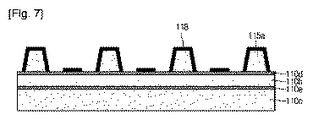
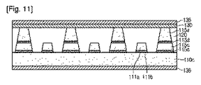
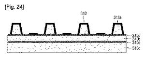
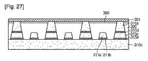
- コア絶縁層と、
前記コア絶縁層を貫通する少なくとも1つのビアと、
前記コア絶縁層の内部に埋め込まれている内部回路層と、
前記コア絶縁層の上部または下部に形成されている外部回路層と、含み、
前記ビアは、第1パート、前記第1パートの下部の第2パート、前記第1及び前記第2パートの間の第3パート、そして前記第1乃至第3パートの間に形成され、前記第1乃至第3パートと互いに異なる金属で形成されている少なくとも1つのバリア層を含み、
前記ビアの前記第3パートの側面は、前記コア絶縁層の上面に対して一定の傾斜角を有し、
前記内部回路層は、前記ビアと分離されており、
前記第1パート、前記第2パート、前記第3パート及び前記バリア層を含む前記ビアの全体構造は、六角形の断面形状を有することを特徴とする印刷回路基板。 - 前記コア絶縁層は、前記ビアの前記第1及び第3パートを埋め込む第1絶縁層と、
前記第1絶縁層の下部に前記ビアの第2パートを埋め込む第2絶縁層と、
を含むことを特徴とする請求項1に記載の印刷回路基板。 - 前記内部回路層は、前記第1絶縁層の下部に埋め込まれる第1回路パートと、前記第2絶縁層の上部に埋め込まれる第2回路パートと、を含み、
前記第1回路パートの厚さは、前記第1絶縁層の厚さより薄く、
前記第2回路パートの厚さは、前記第2絶縁層の厚さより薄いことを特徴とする請求項2に記載の印刷回路基板。 - 前記ビアの前記第1パートの側面は、前記コア絶縁層の上面に対して、前記第3パートの側面が有する傾斜角と同じ傾斜角を有することを特徴とする請求項1乃至3のいずれか1項に記載の印刷回路基板。
- 前記内部回路層は、断面が四角形であることを特徴とする請求項1乃至3のいずれか1項に記載の印刷回路基板。
- 前記バリア層は、前記第1パートと前記第3パートとの間に形成される第1バリア層と、
前記第3パートと前記第2パートとの間に形成され、前記第1バリア層と同一物質で形成される第2バリア層と、を含み、
前記ビアの前記第3パートの上面の幅は、前記第1バリア層の下面の幅と同一であることを特徴とする請求項1乃至3のいずれか1項に記載の印刷回路基板。 - 前記印刷回路基板は、
前記内部回路層及び前記外部回路層を含む2n+1(nは正の整数)の数を有する回路層を含むことを特徴とする請求項1乃至6のいずれか1項に記載の印刷回路基板。 - 前記内部回路層は、下部に前記バリア層を含むことを特徴とする請求項1乃至3のいずれか1項に記載の印刷回路基板。
- 前記コア絶縁層の上部または下部に形成され、前記ビアを露出する接着層をさらに含み、
前記外部回路層は、前記接着層の上に形成されたシード層を含み、
前記シード層の下面は、前記接着層の上面と接触する第1部分と、前記ビアの第1パートの上面と接触する第2部分とを含むことを特徴とする請求項1乃至3のいずれか1項に記載の印刷回路基板。 - 前記接着層は、前記ビアの前記第1パートの側面と接触し、
前記接着層の上面は、前記ビアの前記第1パートの上面と同一平面上に位置することを特徴とする請求項9に記載の印刷回路基板。
Applications Claiming Priority (5)
| Application Number | Priority Date | Filing Date | Title |
|---|---|---|---|
| KR1020100134488A KR101251749B1 (ko) | 2010-12-24 | 2010-12-24 | 인쇄회로기판 및 그의 제조 방법 |
| KR10-2010-0134488 | 2010-12-24 | ||
| KR10-2010-0134489 | 2010-12-24 | ||
| KR1020100134489A KR101231343B1 (ko) | 2010-12-24 | 2010-12-24 | 인쇄회로기판 및 그의 제조 방법 |
| PCT/KR2011/010024 WO2012087058A2 (en) | 2010-12-24 | 2011-12-23 | Printed circuit board and method for manufacturing the same |
Publications (3)
| Publication Number | Publication Date |
|---|---|
| JP2014501448A JP2014501448A (ja) | 2014-01-20 |
| JP2014501448A5 JP2014501448A5 (ja) | 2014-02-27 |
| JP5992923B2 true JP5992923B2 (ja) | 2016-09-14 |
Family
ID=46314659
Family Applications (1)
| Application Number | Title | Priority Date | Filing Date |
|---|---|---|---|
| JP2013546027A Active JP5992923B2 (ja) | 2010-12-24 | 2011-12-23 | 印刷回路基板及びその製造方法 |
Country Status (6)
| Country | Link |
|---|---|
| US (1) | US9572250B2 (ja) |
| EP (1) | EP2656703B1 (ja) |
| JP (1) | JP5992923B2 (ja) |
| CN (1) | CN103404243B (ja) |
| TW (1) | TWI617225B (ja) |
| WO (1) | WO2012087058A2 (ja) |
Families Citing this family (10)
| Publication number | Priority date | Publication date | Assignee | Title |
|---|---|---|---|---|
| CN104768325B (zh) * | 2014-01-08 | 2018-03-23 | 南亚电路板股份有限公司 | 印刷电路板及其制作方法 |
| KR102187695B1 (ko) * | 2014-01-28 | 2020-12-07 | 엘지이노텍 주식회사 | 인쇄회로기판 |
| KR102211741B1 (ko) * | 2014-07-21 | 2021-02-03 | 삼성전기주식회사 | 인쇄회로기판 및 인쇄회로기판의 제조 방법 |
| KR102185067B1 (ko) * | 2014-09-24 | 2020-12-01 | 삼성전기주식회사 | 박막 인덕터용 코일 유닛, 박막 인덕터용 코일 유닛의 제조방법, 박막 인덕터 및 박막 인덕터의 제조방법 |
| KR20160080526A (ko) * | 2014-12-29 | 2016-07-08 | 삼성전기주식회사 | 인쇄회로기판 및 그 제조방법 |
| US10798821B2 (en) | 2016-04-02 | 2020-10-06 | Intel Corporation | Circuit board having a passive device inside a via |
| DE102018102734A1 (de) * | 2018-01-18 | 2019-07-18 | Schreiner Group Gmbh & Co. Kg | Flexible elektrische Schaltung mit Verbindung zwischen elektrisch leitfähigen Strukturelementen |
| KR20200072375A (ko) * | 2018-12-12 | 2020-06-22 | 삼성전기주식회사 | 인쇄회로기판 |
| KR20220098997A (ko) * | 2021-01-05 | 2022-07-12 | 삼성전기주식회사 | 인쇄회로기판 |
| TWI824303B (zh) * | 2021-09-23 | 2023-12-01 | 欣興電子股份有限公司 | 電路板線路結構改良方法及電路板線路改良結構 |
Family Cites Families (28)
| Publication number | Priority date | Publication date | Assignee | Title |
|---|---|---|---|---|
| US5326643A (en) * | 1991-10-07 | 1994-07-05 | International Business Machines Corporation | Adhesive layer in multi-level packaging and organic material as a metal diffusion barrier |
| JPH09116273A (ja) * | 1995-08-11 | 1997-05-02 | Shinko Electric Ind Co Ltd | 多層回路基板及びその製造方法 |
| JPH09181422A (ja) * | 1995-12-25 | 1997-07-11 | Hitachi Aic Inc | プリント配線板の製造方法 |
| US6631558B2 (en) * | 1996-06-05 | 2003-10-14 | Laservia Corporation | Blind via laser drilling system |
| EP1093163B1 (en) | 1997-03-25 | 2004-11-24 | Amitec - Advanced Multilayer Interconnect Technologies Ltd. | Electronic interconnect structure |
| JP4195162B2 (ja) * | 1999-12-21 | 2008-12-10 | 東洋鋼鈑株式会社 | 多層プリント配線板及びその製造方法 |
| US6569543B2 (en) * | 2001-02-15 | 2003-05-27 | Olin Corporation | Copper foil with low profile bond enahncement |
| US6931723B1 (en) * | 2000-09-19 | 2005-08-23 | International Business Machines Corporation | Organic dielectric electronic interconnect structures and method for making |
| JP2002179772A (ja) * | 2000-12-08 | 2002-06-26 | Mitsui Mining & Smelting Co Ltd | プリント配線板の層間絶縁層構成用の樹脂化合物、その樹脂化合物を用いた絶縁層形成用樹脂シート及び樹脂付銅箔、並びにそれらを用いた銅張積層板 |
| US6593534B2 (en) * | 2001-03-19 | 2003-07-15 | International Business Machines Corporation | Printed wiring board structure with z-axis interconnections |
| JP2003133711A (ja) | 2001-10-23 | 2003-05-09 | Matsushita Electric Ind Co Ltd | プリント配線板とその製造方法および電子部品の実装方法 |
| JP4045143B2 (ja) * | 2002-02-18 | 2008-02-13 | テセラ・インターコネクト・マテリアルズ,インコーポレイテッド | 配線膜間接続用部材の製造方法及び多層配線基板の製造方法 |
| CN100383278C (zh) * | 2002-02-28 | 2008-04-23 | 日本瑞翁株式会社 | 部分镀敷方法、部分镀敷树脂基材以及多层电路基板的制造方法 |
| US7548430B1 (en) * | 2002-05-01 | 2009-06-16 | Amkor Technology, Inc. | Buildup dielectric and metallization process and semiconductor package |
| JP2004165544A (ja) | 2002-11-15 | 2004-06-10 | Matsushita Electric Ind Co Ltd | プリント配線板 |
| JP4294967B2 (ja) * | 2003-02-13 | 2009-07-15 | デンカAgsp株式会社 | 多層配線基板及びその製造方法 |
| WO2005007756A1 (ja) * | 2003-05-21 | 2005-01-27 | Hitachi Chemical Co., Ltd. | プライマ、樹脂付き導体箔、積層板並びに積層板の製造方法 |
| JP3949676B2 (ja) * | 2003-07-22 | 2007-07-25 | 三井金属鉱業株式会社 | 極薄接着剤層付銅箔及びその極薄接着剤層付銅箔の製造方法 |
| JP4398683B2 (ja) * | 2003-08-11 | 2010-01-13 | テセラ・インターコネクト・マテリアルズ,インコーポレイテッド | 多層配線基板の製造方法 |
| TWI253714B (en) * | 2004-12-21 | 2006-04-21 | Phoenix Prec Technology Corp | Method for fabricating a multi-layer circuit board with fine pitch |
| US20070281464A1 (en) * | 2006-06-01 | 2007-12-06 | Shih-Ping Hsu | Multi-layer circuit board with fine pitches and fabricating method thereof |
| TWI295911B (en) * | 2006-06-08 | 2008-04-11 | Advanced Semiconductor Eng | Manufacturing method of circuit board |
| US20100233476A1 (en) | 2006-06-20 | 2010-09-16 | Makoto Uchida | Copper foil with primer resin layer and laminated sheet using the same |
| TWM307931U (en) * | 2006-07-07 | 2007-03-11 | Wintek Corp | Single-layer flexible printed circuit board |
| JP2008124370A (ja) * | 2006-11-15 | 2008-05-29 | Hitachi Chem Co Ltd | 多層プリント配線板の製造方法 |
| US9003648B2 (en) * | 2007-01-02 | 2015-04-14 | Ormet Circuits, Inc. | Methods to produce high density, multilayer printed wiring boards from parallel-fabricated circuits and filled vias |
| TW200847867A (en) * | 2007-04-26 | 2008-12-01 | Mitsui Mining & Smelting Co | Printed wire board and manufacturing method thereof, and electrolytic copper foil for copper-clad lamination board used for manufacturing the same |
| JP2009076699A (ja) | 2007-09-20 | 2009-04-09 | Fujikura Ltd | 多層プリント配線板の製造方法 |
-
2011
- 2011-12-20 TW TW100147415A patent/TWI617225B/zh active
- 2011-12-23 WO PCT/KR2011/010024 patent/WO2012087058A2/en active Application Filing
- 2011-12-23 EP EP11851645.9A patent/EP2656703B1/en active Active
- 2011-12-23 US US13/997,464 patent/US9572250B2/en active Active
- 2011-12-23 JP JP2013546027A patent/JP5992923B2/ja active Active
- 2011-12-23 CN CN201180068500.3A patent/CN103404243B/zh active Active
Also Published As
| Publication number | Publication date |
|---|---|
| CN103404243B (zh) | 2017-04-26 |
| EP2656703A2 (en) | 2013-10-30 |
| WO2012087058A2 (en) | 2012-06-28 |
| US20140069705A1 (en) | 2014-03-13 |
| CN103404243A (zh) | 2013-11-20 |
| EP2656703B1 (en) | 2021-08-25 |
| JP2014501448A (ja) | 2014-01-20 |
| EP2656703A4 (en) | 2017-09-13 |
| WO2012087058A3 (en) | 2012-10-04 |
| US9572250B2 (en) | 2017-02-14 |
| TW201247057A (en) | 2012-11-16 |
| TWI617225B (zh) | 2018-03-01 |
Similar Documents
| Publication | Publication Date | Title |
|---|---|---|
| JP5992923B2 (ja) | 印刷回路基板及びその製造方法 | |
| JP5993378B2 (ja) | 印刷回路基板 | |
| US9713267B2 (en) | Method for manufacturing printed wiring board with conductive post and printed wiring board with conductive post | |
| JP6092117B2 (ja) | 印刷回路基板及びその製造方法 | |
| JP2014175485A (ja) | 配線板及びその製造方法 | |
| TWI442854B (zh) | 印刷電路板及其製造方法 | |
| TW200412205A (en) | Double-sided printed circuit board without via holes and method of fabricating the same | |
| JP6214398B2 (ja) | 印刷回路基板 | |
| JP2023022267A (ja) | プリント回路基板 | |
| KR101905879B1 (ko) | 인쇄회로기판 및 그의 제조 방법 | |
| TWI446843B (zh) | 線路板及其製程 | |
| US11160164B2 (en) | Wiring substrate | |
| KR20110064216A (ko) | 범프를 구비한 회로기판 및 그 제조 방법 | |
| JP7389666B2 (ja) | リジッド・フレックス多層プリント配線板の製造方法 | |
| KR101987378B1 (ko) | 인쇄회로기판의 제조 방법 | |
| KR101231273B1 (ko) | 인쇄회로기판 및 그의 제조 방법 | |
| KR101231343B1 (ko) | 인쇄회로기판 및 그의 제조 방법 | |
| JP2018182252A (ja) | プリント配線板の製造方法 | |
| KR101251749B1 (ko) | 인쇄회로기판 및 그의 제조 방법 | |
| KR101154700B1 (ko) | 인쇄회로기판 및 그의 제조 방법 | |
| KR101262584B1 (ko) | 인쇄회로기판 및 그의 제조 방법 | |
| KR101154720B1 (ko) | 인쇄회로기판 및 그의 제조 방법 | |
| KR101231525B1 (ko) | 인쇄회로기판 및 그의 제조 방법 | |
| KR101905881B1 (ko) | 인쇄회로기판 및 그의 제조 방법 | |
| KR101262513B1 (ko) | 인쇄회로기판 및 그의 제조 방법 |
Legal Events
| Date | Code | Title | Description |
|---|---|---|---|
| A521 | Request for written amendment filed |
Free format text: JAPANESE INTERMEDIATE CODE: A523 Effective date: 20131206 |
|
| A072 | Dismissal of procedure [no reply to invitation to correct request for examination] |
Free format text: JAPANESE INTERMEDIATE CODE: A072 Effective date: 20140218 |
|
| A621 | Written request for application examination |
Free format text: JAPANESE INTERMEDIATE CODE: A621 Effective date: 20141210 |
|
| A977 | Report on retrieval |
Free format text: JAPANESE INTERMEDIATE CODE: A971007 Effective date: 20150710 |
|
| A131 | Notification of reasons for refusal |
Free format text: JAPANESE INTERMEDIATE CODE: A131 Effective date: 20150721 |
|
| A521 | Request for written amendment filed |
Free format text: JAPANESE INTERMEDIATE CODE: A523 Effective date: 20151013 |
|
| A02 | Decision of refusal |
Free format text: JAPANESE INTERMEDIATE CODE: A02 Effective date: 20160112 |
|
| A521 | Request for written amendment filed |
Free format text: JAPANESE INTERMEDIATE CODE: A523 Effective date: 20160510 |
|
| A911 | Transfer to examiner for re-examination before appeal (zenchi) |
Free format text: JAPANESE INTERMEDIATE CODE: A911 Effective date: 20160518 |
|
| TRDD | Decision of grant or rejection written | ||
| A01 | Written decision to grant a patent or to grant a registration (utility model) |
Free format text: JAPANESE INTERMEDIATE CODE: A01 Effective date: 20160719 |
|
| A61 | First payment of annual fees (during grant procedure) |
Free format text: JAPANESE INTERMEDIATE CODE: A61 Effective date: 20160818 |
|
| R150 | Certificate of patent or registration of utility model |
Ref document number: 5992923 Country of ref document: JP Free format text: JAPANESE INTERMEDIATE CODE: R150 |
|
| R250 | Receipt of annual fees |
Free format text: JAPANESE INTERMEDIATE CODE: R250 |
|
| R250 | Receipt of annual fees |
Free format text: JAPANESE INTERMEDIATE CODE: R250 |
|
| R250 | Receipt of annual fees |
Free format text: JAPANESE INTERMEDIATE CODE: R250 |
|
| R250 | Receipt of annual fees |
Free format text: JAPANESE INTERMEDIATE CODE: R250 |
|
| R250 | Receipt of annual fees |
Free format text: JAPANESE INTERMEDIATE CODE: R250 |