JP6092117B2 - 印刷回路基板及びその製造方法 - Google Patents
印刷回路基板及びその製造方法 Download PDFInfo
- Publication number
- JP6092117B2 JP6092117B2 JP2013546035A JP2013546035A JP6092117B2 JP 6092117 B2 JP6092117 B2 JP 6092117B2 JP 2013546035 A JP2013546035 A JP 2013546035A JP 2013546035 A JP2013546035 A JP 2013546035A JP 6092117 B2 JP6092117 B2 JP 6092117B2
- Authority
- JP
- Japan
- Prior art keywords
- bump
- circuit board
- printed circuit
- solder resist
- width
- Prior art date
- Legal status (The legal status is an assumption and is not a legal conclusion. Google has not performed a legal analysis and makes no representation as to the accuracy of the status listed.)
- Active
Links
- 238000004519 manufacturing process Methods 0.000 title description 25
- 229910000679 solder Inorganic materials 0.000 claims description 85
- RYGMFSIKBFXOCR-UHFFFAOYSA-N Copper Chemical compound [Cu] RYGMFSIKBFXOCR-UHFFFAOYSA-N 0.000 claims description 15
- 229910052802 copper Inorganic materials 0.000 claims description 14
- 239000010949 copper Substances 0.000 claims description 14
- 229910045601 alloy Inorganic materials 0.000 claims description 12
- 239000000956 alloy Substances 0.000 claims description 12
- 238000007747 plating Methods 0.000 description 27
- 238000000034 method Methods 0.000 description 25
- 239000002184 metal Substances 0.000 description 18
- 229910052751 metal Inorganic materials 0.000 description 18
- 239000000758 substrate Substances 0.000 description 14
- 238000007772 electroless plating Methods 0.000 description 7
- PXHVJJICTQNCMI-UHFFFAOYSA-N Nickel Chemical compound [Ni] PXHVJJICTQNCMI-UHFFFAOYSA-N 0.000 description 4
- 239000004020 conductor Substances 0.000 description 4
- 238000009751 slip forming Methods 0.000 description 4
- 238000005530 etching Methods 0.000 description 3
- 238000011156 evaluation Methods 0.000 description 3
- 239000004593 Epoxy Substances 0.000 description 2
- 229910020888 Sn-Cu Inorganic materials 0.000 description 2
- 229910019204 Sn—Cu Inorganic materials 0.000 description 2
- 239000000654 additive Substances 0.000 description 2
- 239000000919 ceramic Substances 0.000 description 2
- 238000007796 conventional method Methods 0.000 description 2
- 238000009713 electroplating Methods 0.000 description 2
- 239000011521 glass Substances 0.000 description 2
- 229910003471 inorganic composite material Inorganic materials 0.000 description 2
- 229910052759 nickel Inorganic materials 0.000 description 2
- 229920001721 polyimide Polymers 0.000 description 2
- 239000009719 polyimide resin Substances 0.000 description 2
- 239000002952 polymeric resin Substances 0.000 description 2
- 239000011347 resin Substances 0.000 description 2
- 229920005989 resin Polymers 0.000 description 2
- 229920003002 synthetic resin Polymers 0.000 description 2
- 229920001169 thermoplastic Polymers 0.000 description 2
- 229920001187 thermosetting polymer Polymers 0.000 description 2
- 238000001994 activation Methods 0.000 description 1
- 230000000996 additive effect Effects 0.000 description 1
- 239000003963 antioxidant agent Substances 0.000 description 1
- 230000003078 antioxidant effect Effects 0.000 description 1
- 230000015572 biosynthetic process Effects 0.000 description 1
- 239000003054 catalyst Substances 0.000 description 1
- 239000011889 copper foil Substances 0.000 description 1
- 230000007797 corrosion Effects 0.000 description 1
- 238000005260 corrosion Methods 0.000 description 1
- 230000007547 defect Effects 0.000 description 1
- 238000005238 degreasing Methods 0.000 description 1
- 238000011161 development Methods 0.000 description 1
- 239000002923 metal particle Substances 0.000 description 1
- 238000012986 modification Methods 0.000 description 1
- 230000004048 modification Effects 0.000 description 1
- 238000000059 patterning Methods 0.000 description 1
- 239000012041 precatalyst Substances 0.000 description 1
- 238000004088 simulation Methods 0.000 description 1
- 238000004544 sputter deposition Methods 0.000 description 1
- 239000000126 substance Substances 0.000 description 1
- 238000004381 surface treatment Methods 0.000 description 1
Images


Classifications
-
- H—ELECTRICITY
- H05—ELECTRIC TECHNIQUES NOT OTHERWISE PROVIDED FOR
- H05K—PRINTED CIRCUITS; CASINGS OR CONSTRUCTIONAL DETAILS OF ELECTRIC APPARATUS; MANUFACTURE OF ASSEMBLAGES OF ELECTRICAL COMPONENTS
- H05K1/00—Printed circuits
- H05K1/02—Details
-
- H—ELECTRICITY
- H05—ELECTRIC TECHNIQUES NOT OTHERWISE PROVIDED FOR
- H05K—PRINTED CIRCUITS; CASINGS OR CONSTRUCTIONAL DETAILS OF ELECTRIC APPARATUS; MANUFACTURE OF ASSEMBLAGES OF ELECTRICAL COMPONENTS
- H05K3/00—Apparatus or processes for manufacturing printed circuits
- H05K3/40—Forming printed elements for providing electric connections to or between printed circuits
- H05K3/4007—Surface contacts, e.g. bumps
-
- H—ELECTRICITY
- H05—ELECTRIC TECHNIQUES NOT OTHERWISE PROVIDED FOR
- H05K—PRINTED CIRCUITS; CASINGS OR CONSTRUCTIONAL DETAILS OF ELECTRIC APPARATUS; MANUFACTURE OF ASSEMBLAGES OF ELECTRICAL COMPONENTS
- H05K2201/00—Indexing scheme relating to printed circuits covered by H05K1/00
- H05K2201/03—Conductive materials
- H05K2201/0332—Structure of the conductor
- H05K2201/0364—Conductor shape
- H05K2201/0367—Metallic bump or raised conductor not used as solder bump
-
- H—ELECTRICITY
- H05—ELECTRIC TECHNIQUES NOT OTHERWISE PROVIDED FOR
- H05K—PRINTED CIRCUITS; CASINGS OR CONSTRUCTIONAL DETAILS OF ELECTRIC APPARATUS; MANUFACTURE OF ASSEMBLAGES OF ELECTRICAL COMPONENTS
- H05K3/00—Apparatus or processes for manufacturing printed circuits
- H05K3/30—Assembling printed circuits with electric components, e.g. with resistor
- H05K3/32—Assembling printed circuits with electric components, e.g. with resistor electrically connecting electric components or wires to printed circuits
- H05K3/34—Assembling printed circuits with electric components, e.g. with resistor electrically connecting electric components or wires to printed circuits by soldering
- H05K3/341—Surface mounted components
- H05K3/3431—Leadless components
- H05K3/3436—Leadless components having an array of bottom contacts, e.g. pad grid array or ball grid array components
-
- H—ELECTRICITY
- H05—ELECTRIC TECHNIQUES NOT OTHERWISE PROVIDED FOR
- H05K—PRINTED CIRCUITS; CASINGS OR CONSTRUCTIONAL DETAILS OF ELECTRIC APPARATUS; MANUFACTURE OF ASSEMBLAGES OF ELECTRICAL COMPONENTS
- H05K3/00—Apparatus or processes for manufacturing printed circuits
- H05K3/30—Assembling printed circuits with electric components, e.g. with resistor
- H05K3/32—Assembling printed circuits with electric components, e.g. with resistor electrically connecting electric components or wires to printed circuits
- H05K3/34—Assembling printed circuits with electric components, e.g. with resistor electrically connecting electric components or wires to printed circuits by soldering
- H05K3/3452—Solder masks
Landscapes
- Engineering & Computer Science (AREA)
- Microelectronics & Electronic Packaging (AREA)
- Manufacturing & Machinery (AREA)
- Electric Connection Of Electric Components To Printed Circuits (AREA)
- Non-Metallic Protective Coatings For Printed Circuits (AREA)
Description
前記絶縁プレート110は熱硬化性または熱可塑性高分子基板、セラミック基板、有−無機複合素材基板、またはガラス繊維含浸基板であることがあり、高分子樹脂を含む場合、エポキシ系絶縁樹脂を含むことができ、これとは異なり、ポリイミド系樹脂を含むこともできる。
Claims (3)
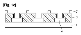
- 絶縁層と、
前記絶縁層の上に配置されるパッドと、
前記絶縁層の上に配置され、前記パッドの上面を露出する開口部を有するソルダーレジストと、
前記開口部を通じて露出された前記パッドの上面の上に配置され、前記開口部を埋め込みながら前記ソルダーレジストの表面上に突出した第1部分と、前記第1部分の上に配置された第2部分とを含むバンプ連結部と、
前記バンプ連結部の前記第2部分の上に配置されるバンプと、
前記バンプの上に配置されるソルダーと、を含み、
前記バンプ連結部の前記第1部分の幅は前記ソルダーレジストの前記開口部の幅より狭く、
前記バンプ連結部は、前記第2部分の幅が前記第1部分の幅より狭く、
前記バンプは、上面及び下面の幅が前記バンプ連結部の前記第2部分の幅と同一であり、
前記ソルダーは、上面及び下面の幅が前記バンプの上面の幅と同一であることを特徴とする、印刷回路基板。 - 前記バンプは、円柱、四角柱、及び多角柱のうち、少なくともいずれか1つの形状を有することを特徴とする、請求項1に記載の印刷回路基板。
- 前記バンプは銅を含む合金で形成されていることを特徴とする、請求項1または2に記載の印刷回路基板。
Applications Claiming Priority (5)
| Application Number | Priority Date | Filing Date | Title |
|---|---|---|---|
| KR1020100134543A KR101189337B1 (ko) | 2010-12-24 | 2010-12-24 | 인쇄회로기판 및 그의 제조 방법 |
| KR10-2010-0134543 | 2010-12-24 | ||
| KR10-2011-0052487 | 2011-05-31 | ||
| KR1020110052487A KR101231263B1 (ko) | 2011-05-31 | 2011-05-31 | 인쇄회로기판 및 그의 제조 방법 |
| PCT/KR2011/010058 WO2012087073A2 (ko) | 2010-12-24 | 2011-12-23 | 인쇄회로기판 및 그의 제조 방법 |
Publications (3)
| Publication Number | Publication Date |
|---|---|
| JP2014501451A JP2014501451A (ja) | 2014-01-20 |
| JP2014501451A5 JP2014501451A5 (ja) | 2014-11-27 |
| JP6092117B2 true JP6092117B2 (ja) | 2017-03-08 |
Family
ID=46314671
Family Applications (1)
| Application Number | Title | Priority Date | Filing Date |
|---|---|---|---|
| JP2013546035A Active JP6092117B2 (ja) | 2010-12-24 | 2011-12-23 | 印刷回路基板及びその製造方法 |
Country Status (6)
| Country | Link |
|---|---|
| US (1) | US9363883B2 (ja) |
| EP (1) | EP2645828B1 (ja) |
| JP (1) | JP6092117B2 (ja) |
| CN (1) | CN103416108B (ja) |
| TW (1) | TWI449485B (ja) |
| WO (1) | WO2012087073A2 (ja) |
Families Citing this family (8)
| Publication number | Priority date | Publication date | Assignee | Title |
|---|---|---|---|---|
| US20130168132A1 (en) * | 2011-12-29 | 2013-07-04 | Sumsung Electro-Mechanics Co., Ltd. | Printed circuit board and method of manufacturing the same |
| KR102152865B1 (ko) * | 2014-02-06 | 2020-09-07 | 엘지이노텍 주식회사 | 인쇄회로기판, 이를 포함하는 패키지 기판 및 이의 제조 방법 |
| JP2016076534A (ja) * | 2014-10-03 | 2016-05-12 | イビデン株式会社 | 金属ポスト付きプリント配線板およびその製造方法 |
| CN107509319A (zh) * | 2016-06-14 | 2017-12-22 | 华为终端(东莞)有限公司 | 一种底部有焊端的模块 |
| US10057989B1 (en) * | 2017-04-10 | 2018-08-21 | Tactotek Oy | Multilayer structure and related method of manufacture for electronics |
| TWI711133B (zh) * | 2019-07-26 | 2020-11-21 | 大陸商上海兆芯集成電路有限公司 | 電子結構及其製造方法 |
| WO2021019675A1 (ja) * | 2019-07-30 | 2021-02-04 | 株式会社Fuji | 3次元積層造形による電子回路製造方法 |
| CN114571021A (zh) * | 2021-10-12 | 2022-06-03 | 祥博传热科技股份有限公司 | 一种高导热覆铜陶瓷基板制作方法 |
Family Cites Families (26)
| Publication number | Priority date | Publication date | Assignee | Title |
|---|---|---|---|---|
| JPH02310941A (ja) * | 1989-05-26 | 1990-12-26 | Mitsui Mining & Smelting Co Ltd | バンプを有するプリント回路基板およびバンプの形成方法 |
| JP2002134545A (ja) * | 2000-10-26 | 2002-05-10 | Oki Electric Ind Co Ltd | 半導体集積回路チップ及び基板、並びにその製造方法 |
| JP2002261111A (ja) | 2001-03-06 | 2002-09-13 | Texas Instr Japan Ltd | 半導体装置及びバンプ形成方法 |
| JP2003142811A (ja) | 2001-11-06 | 2003-05-16 | Ngk Spark Plug Co Ltd | 配線基板及び配線基板の製造方法 |
| JP2003152320A (ja) * | 2001-11-09 | 2003-05-23 | Ngk Spark Plug Co Ltd | 配線基板及び配線基板の製造方法 |
| JP2003198085A (ja) * | 2001-12-25 | 2003-07-11 | Shinko Electric Ind Co Ltd | 回路基板およびその製造方法 |
| JP2005108941A (ja) * | 2003-09-29 | 2005-04-21 | Toppan Printing Co Ltd | 多層配線板及びその製造方法 |
| JP4665531B2 (ja) | 2005-01-27 | 2011-04-06 | 日立電線株式会社 | 配線板の製造方法 |
| TWI286454B (en) * | 2005-03-09 | 2007-09-01 | Phoenix Prec Technology Corp | Electrical connector structure of circuit board and method for fabricating the same |
| TWI281840B (en) | 2005-05-09 | 2007-05-21 | Phoenix Prec Technology Corp | Electrically connecting structure of circuit board and method for fabricating same |
| KR100743233B1 (ko) | 2005-07-18 | 2007-07-27 | 엘지전자 주식회사 | 인쇄회로기판의 패드 및 그 제조방법 |
| KR100703663B1 (ko) | 2005-07-26 | 2007-04-06 | 엘지전자 주식회사 | 인쇄회로기판 및 그 제조방법 |
| TWI292684B (en) | 2006-02-09 | 2008-01-11 | Phoenix Prec Technology Corp | Method for fabricating circuit board with conductive structure |
| TWI319966B (en) * | 2006-06-14 | 2010-01-21 | A method of manufacturing a substrate having metal bumps | |
| KR100832651B1 (ko) | 2007-06-20 | 2008-05-27 | 삼성전기주식회사 | 인쇄회로기판 |
| JP5114130B2 (ja) | 2007-08-24 | 2013-01-09 | 新光電気工業株式会社 | 配線基板及びその製造方法、及び半導体装置 |
| TWI345433B (en) * | 2008-02-27 | 2011-07-11 | Unimicron Technology Corp | Circuit board having conductive bumps and fabrication method thereof |
| KR100959856B1 (ko) * | 2008-03-17 | 2010-05-27 | 삼성전기주식회사 | 인쇄회로기판 제조방법 |
| JP2010003793A (ja) * | 2008-06-19 | 2010-01-07 | Fujitsu Ltd | 配線基板、ポスト電極の転写用基板及び電子機器 |
| KR100986294B1 (ko) * | 2008-07-28 | 2010-10-07 | 삼성전기주식회사 | 인쇄회로기판의 제조방법 |
| CN102187749A (zh) * | 2008-10-21 | 2011-09-14 | 埃托特克德国有限公司 | 用于在衬底上形成焊料沉积物的方法 |
| CN101754592A (zh) * | 2008-11-28 | 2010-06-23 | 欣兴电子股份有限公司 | 导电凸块的制造方法及具有导电凸块的电路板结构 |
| KR101140882B1 (ko) | 2009-08-31 | 2012-05-03 | 삼성전기주식회사 | 범프를 구비한 인쇄회로기판 및 그 제조방법 |
| KR101156917B1 (ko) | 2010-05-24 | 2012-06-21 | 삼성전기주식회사 | 반도체 패키지 기판 및 그 제조방법 |
| JP2012054295A (ja) * | 2010-08-31 | 2012-03-15 | Kyocer Slc Technologies Corp | 配線基板およびその製造方法 |
| KR101199174B1 (ko) | 2010-09-27 | 2012-11-07 | 엘지이노텍 주식회사 | 인쇄회로기판 및 그의 제조 방법 |
-
2011
- 2011-12-23 US US13/997,420 patent/US9363883B2/en active Active
- 2011-12-23 JP JP2013546035A patent/JP6092117B2/ja active Active
- 2011-12-23 EP EP11851669.9A patent/EP2645828B1/en active Active
- 2011-12-23 WO PCT/KR2011/010058 patent/WO2012087073A2/ko active Application Filing
- 2011-12-23 CN CN201180068544.6A patent/CN103416108B/zh active Active
- 2011-12-26 TW TW100148570A patent/TWI449485B/zh active
Also Published As
| Publication number | Publication date |
|---|---|
| EP2645828A2 (en) | 2013-10-02 |
| CN103416108B (zh) | 2016-11-02 |
| CN103416108A (zh) | 2013-11-27 |
| WO2012087073A2 (ko) | 2012-06-28 |
| JP2014501451A (ja) | 2014-01-20 |
| TWI449485B (zh) | 2014-08-11 |
| US20140000951A1 (en) | 2014-01-02 |
| EP2645828B1 (en) | 2019-11-13 |
| WO2012087073A3 (ko) | 2012-09-27 |
| TW201236530A (en) | 2012-09-01 |
| US9363883B2 (en) | 2016-06-07 |
| EP2645828A4 (en) | 2018-01-17 |
Similar Documents
| Publication | Publication Date | Title |
|---|---|---|
| JP6092117B2 (ja) | 印刷回路基板及びその製造方法 | |
| TWI475938B (zh) | 多層配線板及其製造方法 | |
| US9572250B2 (en) | Printed circuit board and method for manufacturing the same | |
| JP2010135721A (ja) | 金属バンプを持つプリント基板及びその製造方法 | |
| TWI442854B (zh) | 印刷電路板及其製造方法 | |
| JP2016100599A (ja) | プリント回路基板、その製造方法、及び電子部品モジュール | |
| JP6214398B2 (ja) | 印刷回路基板 | |
| JP5762376B2 (ja) | 配線基板及びその製造方法 | |
| KR101219905B1 (ko) | 인쇄회로기판 및 그의 제조 방법 | |
| KR20110064216A (ko) | 범프를 구비한 회로기판 및 그 제조 방법 | |
| KR101199174B1 (ko) | 인쇄회로기판 및 그의 제조 방법 | |
| KR101189337B1 (ko) | 인쇄회로기판 및 그의 제조 방법 | |
| TWI398205B (zh) | 印刷電路基板的製造方法 | |
| KR100688697B1 (ko) | 패키지 기판의 제조방법 | |
| KR101231522B1 (ko) | 인쇄회로기판 및 그의 제조 방법 | |
| KR101231263B1 (ko) | 인쇄회로기판 및 그의 제조 방법 | |
| KR20150107141A (ko) | 인쇄회로기판 및 그의 제조 방법 | |
| KR100815322B1 (ko) | 인쇄회로기판 및 그 제조방법 | |
| KR101154700B1 (ko) | 인쇄회로기판 및 그의 제조 방법 | |
| KR101231343B1 (ko) | 인쇄회로기판 및 그의 제조 방법 | |
| KR101189330B1 (ko) | 인쇄회로기판 및 그의 제조 방법 | |
| KR101173397B1 (ko) | 인쇄회로기판의 제조 방법 | |
| JP2022115401A (ja) | 配線基板及び配線基板の製造方法 | |
| KR101730468B1 (ko) | 범프가 포함된 인쇄회로기판 및 그 제조방법 | |
| KR101231525B1 (ko) | 인쇄회로기판 및 그의 제조 방법 |
Legal Events
| Date | Code | Title | Description |
|---|---|---|---|
| A521 | Request for written amendment filed |
Free format text: JAPANESE INTERMEDIATE CODE: A523 Effective date: 20141002 |
|
| A621 | Written request for application examination |
Free format text: JAPANESE INTERMEDIATE CODE: A621 Effective date: 20141210 |
|
| A977 | Report on retrieval |
Free format text: JAPANESE INTERMEDIATE CODE: A971007 Effective date: 20150928 |
|
| A131 | Notification of reasons for refusal |
Free format text: JAPANESE INTERMEDIATE CODE: A131 Effective date: 20150929 |
|
| A521 | Request for written amendment filed |
Free format text: JAPANESE INTERMEDIATE CODE: A523 Effective date: 20151228 |
|
| A131 | Notification of reasons for refusal |
Free format text: JAPANESE INTERMEDIATE CODE: A131 Effective date: 20160607 |
|
| A521 | Request for written amendment filed |
Free format text: JAPANESE INTERMEDIATE CODE: A523 Effective date: 20160830 |
|
| TRDD | Decision of grant or rejection written | ||
| A01 | Written decision to grant a patent or to grant a registration (utility model) |
Free format text: JAPANESE INTERMEDIATE CODE: A01 Effective date: 20170131 |
|
| A61 | First payment of annual fees (during grant procedure) |
Free format text: JAPANESE INTERMEDIATE CODE: A61 Effective date: 20170208 |
|
| R150 | Certificate of patent or registration of utility model |
Ref document number: 6092117 Country of ref document: JP Free format text: JAPANESE INTERMEDIATE CODE: R150 |
|
| R250 | Receipt of annual fees |
Free format text: JAPANESE INTERMEDIATE CODE: R250 |
|
| R250 | Receipt of annual fees |
Free format text: JAPANESE INTERMEDIATE CODE: R250 |
|
| R250 | Receipt of annual fees |
Free format text: JAPANESE INTERMEDIATE CODE: R250 |
|
| R250 | Receipt of annual fees |
Free format text: JAPANESE INTERMEDIATE CODE: R250 |
|
| R250 | Receipt of annual fees |
Free format text: JAPANESE INTERMEDIATE CODE: R250 |