JP5721178B2 - 拡幅活性領域を有する半導体素子 - Google Patents
拡幅活性領域を有する半導体素子 Download PDFInfo
- Publication number
- JP5721178B2 JP5721178B2 JP2011521138A JP2011521138A JP5721178B2 JP 5721178 B2 JP5721178 B2 JP 5721178B2 JP 2011521138 A JP2011521138 A JP 2011521138A JP 2011521138 A JP2011521138 A JP 2011521138A JP 5721178 B2 JP5721178 B2 JP 5721178B2
- Authority
- JP
- Japan
- Prior art keywords
- active region
- forming
- trench
- region
- mask pattern
- Prior art date
- Legal status (The legal status is an assumption and is not a legal conclusion. Google has not performed a legal analysis and makes no representation as to the accuracy of the status listed.)
- Active
Links
- 239000004065 semiconductor Substances 0.000 title claims description 47
- 238000000034 method Methods 0.000 claims description 57
- 238000002955 isolation Methods 0.000 claims description 18
- 238000005530 etching Methods 0.000 claims description 10
- 239000000463 material Substances 0.000 claims description 9
- 239000000758 substrate Substances 0.000 claims description 9
- 239000011810 insulating material Substances 0.000 claims description 6
- 229920002120 photoresistant polymer Polymers 0.000 claims description 6
- 238000005498 polishing Methods 0.000 claims description 6
- 239000000126 substance Substances 0.000 claims description 5
- 238000009966 trimming Methods 0.000 claims description 5
- 238000004380 ashing Methods 0.000 claims description 3
- 238000000926 separation method Methods 0.000 claims 1
- 229910052710 silicon Inorganic materials 0.000 description 11
- 239000010703 silicon Substances 0.000 description 11
- XUIMIQQOPSSXEZ-UHFFFAOYSA-N Silicon Chemical compound [Si] XUIMIQQOPSSXEZ-UHFFFAOYSA-N 0.000 description 10
- KRHYYFGTRYWZRS-UHFFFAOYSA-N Fluorane Chemical compound F KRHYYFGTRYWZRS-UHFFFAOYSA-N 0.000 description 5
- 239000013078 crystal Substances 0.000 description 3
- 238000005516 engineering process Methods 0.000 description 3
- 150000004767 nitrides Chemical class 0.000 description 3
- NBIIXXVUZAFLBC-UHFFFAOYSA-N Phosphoric acid Chemical compound OP(O)(O)=O NBIIXXVUZAFLBC-UHFFFAOYSA-N 0.000 description 2
- 238000001312 dry etching Methods 0.000 description 2
- 238000012986 modification Methods 0.000 description 2
- 230000004048 modification Effects 0.000 description 2
- JBRZTFJDHDCESZ-UHFFFAOYSA-N AsGa Chemical compound [As]#[Ga] JBRZTFJDHDCESZ-UHFFFAOYSA-N 0.000 description 1
- 229910001218 Gallium arsenide Inorganic materials 0.000 description 1
- 229910000577 Silicon-germanium Inorganic materials 0.000 description 1
- LEVVHYCKPQWKOP-UHFFFAOYSA-N [Si].[Ge] Chemical compound [Si].[Ge] LEVVHYCKPQWKOP-UHFFFAOYSA-N 0.000 description 1
- 229910000147 aluminium phosphate Inorganic materials 0.000 description 1
- 239000002131 composite material Substances 0.000 description 1
- 230000000694 effects Effects 0.000 description 1
- 238000007373 indentation Methods 0.000 description 1
- 238000009413 insulation Methods 0.000 description 1
- 239000012212 insulator Substances 0.000 description 1
- 238000004519 manufacturing process Methods 0.000 description 1
- 229910021421 monocrystalline silicon Inorganic materials 0.000 description 1
- QPJSUIGXIBEQAC-UHFFFAOYSA-N n-(2,4-dichloro-5-propan-2-yloxyphenyl)acetamide Chemical compound CC(C)OC1=CC(NC(C)=O)=C(Cl)C=C1Cl QPJSUIGXIBEQAC-UHFFFAOYSA-N 0.000 description 1
- 238000000059 patterning Methods 0.000 description 1
- 150000003376 silicon Chemical class 0.000 description 1
- 125000006850 spacer group Chemical group 0.000 description 1
- 230000002123 temporal effect Effects 0.000 description 1
Images


Classifications
-
- H—ELECTRICITY
- H01—ELECTRIC ELEMENTS
- H01L—SEMICONDUCTOR DEVICES NOT COVERED BY CLASS H10
- H01L21/00—Processes or apparatus adapted for the manufacture or treatment of semiconductor or solid state devices or of parts thereof
- H01L21/70—Manufacture or treatment of devices consisting of a plurality of solid state components formed in or on a common substrate or of parts thereof; Manufacture of integrated circuit devices or of parts thereof
- H01L21/71—Manufacture of specific parts of devices defined in group H01L21/70
- H01L21/76—Making of isolation regions between components
- H01L21/762—Dielectric regions, e.g. EPIC dielectric isolation, LOCOS; Trench refilling techniques, SOI technology, use of channel stoppers
- H01L21/76224—Dielectric regions, e.g. EPIC dielectric isolation, LOCOS; Trench refilling techniques, SOI technology, use of channel stoppers using trench refilling with dielectric materials
- H01L21/76232—Dielectric regions, e.g. EPIC dielectric isolation, LOCOS; Trench refilling techniques, SOI technology, use of channel stoppers using trench refilling with dielectric materials of trenches having a shape other than rectangular or V-shape, e.g. rounded corners, oblique or rounded trench walls
-
- H—ELECTRICITY
- H01—ELECTRIC ELEMENTS
- H01L—SEMICONDUCTOR DEVICES NOT COVERED BY CLASS H10
- H01L27/00—Devices consisting of a plurality of semiconductor or other solid-state components formed in or on a common substrate
- H01L27/02—Devices consisting of a plurality of semiconductor or other solid-state components formed in or on a common substrate including semiconductor components specially adapted for rectifying, oscillating, amplifying or switching and having at least one potential-jump barrier or surface barrier; including integrated passive circuit elements with at least one potential-jump barrier or surface barrier
- H01L27/0203—Particular design considerations for integrated circuits
- H01L27/0207—Geometrical layout of the components, e.g. computer aided design; custom LSI, semi-custom LSI, standard cell technique
-
- H—ELECTRICITY
- H01—ELECTRIC ELEMENTS
- H01L—SEMICONDUCTOR DEVICES NOT COVERED BY CLASS H10
- H01L21/00—Processes or apparatus adapted for the manufacture or treatment of semiconductor or solid state devices or of parts thereof
- H01L21/70—Manufacture or treatment of devices consisting of a plurality of solid state components formed in or on a common substrate or of parts thereof; Manufacture of integrated circuit devices or of parts thereof
- H01L21/77—Manufacture or treatment of devices consisting of a plurality of solid state components or integrated circuits formed in, or on, a common substrate
- H01L21/78—Manufacture or treatment of devices consisting of a plurality of solid state components or integrated circuits formed in, or on, a common substrate with subsequent division of the substrate into plural individual devices
- H01L21/82—Manufacture or treatment of devices consisting of a plurality of solid state components or integrated circuits formed in, or on, a common substrate with subsequent division of the substrate into plural individual devices to produce devices, e.g. integrated circuits, each consisting of a plurality of components
- H01L21/8252—Manufacture or treatment of devices consisting of a plurality of solid state components or integrated circuits formed in, or on, a common substrate with subsequent division of the substrate into plural individual devices to produce devices, e.g. integrated circuits, each consisting of a plurality of components the substrate being a semiconductor, using III-V technology
-
- H—ELECTRICITY
- H01—ELECTRIC ELEMENTS
- H01L—SEMICONDUCTOR DEVICES NOT COVERED BY CLASS H10
- H01L21/00—Processes or apparatus adapted for the manufacture or treatment of semiconductor or solid state devices or of parts thereof
- H01L21/70—Manufacture or treatment of devices consisting of a plurality of solid state components formed in or on a common substrate or of parts thereof; Manufacture of integrated circuit devices or of parts thereof
- H01L21/77—Manufacture or treatment of devices consisting of a plurality of solid state components or integrated circuits formed in, or on, a common substrate
- H01L21/78—Manufacture or treatment of devices consisting of a plurality of solid state components or integrated circuits formed in, or on, a common substrate with subsequent division of the substrate into plural individual devices
- H01L21/82—Manufacture or treatment of devices consisting of a plurality of solid state components or integrated circuits formed in, or on, a common substrate with subsequent division of the substrate into plural individual devices to produce devices, e.g. integrated circuits, each consisting of a plurality of components
- H01L21/84—Manufacture or treatment of devices consisting of a plurality of solid state components or integrated circuits formed in, or on, a common substrate with subsequent division of the substrate into plural individual devices to produce devices, e.g. integrated circuits, each consisting of a plurality of components the substrate being other than a semiconductor body, e.g. being an insulating body
-
- H—ELECTRICITY
- H10—SEMICONDUCTOR DEVICES; ELECTRIC SOLID-STATE DEVICES NOT OTHERWISE PROVIDED FOR
- H10B—ELECTRONIC MEMORY DEVICES
- H10B10/00—Static random access memory [SRAM] devices
Landscapes
- Engineering & Computer Science (AREA)
- Power Engineering (AREA)
- Computer Hardware Design (AREA)
- Condensed Matter Physics & Semiconductors (AREA)
- General Physics & Mathematics (AREA)
- Physics & Mathematics (AREA)
- Microelectronics & Electronic Packaging (AREA)
- General Engineering & Computer Science (AREA)
- Manufacturing & Machinery (AREA)
- Element Separation (AREA)
- Metal-Oxide And Bipolar Metal-Oxide Semiconductor Integrated Circuits (AREA)
- Semiconductor Memories (AREA)
- Recrystallisation Techniques (AREA)
Description
Claims (13)
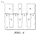
- プレーナ型の半導体素子を半導体層の内部から上方にわたって形成するための方法において、
トレンチを第1活性領域に隣接して形成する工程と、
前記トレンチに絶縁材料を充填する工程と、
前記トレンチのうち、マスクパターンの第1側部と前記第1活性領域との間に位置する第1側部を露出させるように、マスクパターンを前記トレンチの中央部分の上に形成する工程と、
第1窪みを前記トレンチに残すために、前記トレンチの前記第1側部を掘り込むエッチングを行う工程と、
第1エピタキシャル領域が前記第1窪みを完全に充填するように前記第1エピタキシャル領域を前記第1窪みに成長させて、前記第1活性領域を延長して前記第1窪みを含むように、第1拡幅活性領域を形成する工程と、
プレーナ型のトランジスタを前記第1拡幅活性領域の内部から上方にわたって、チャネルの上に第1方向に延在するゲートを有するように形成する工程を備え、
前記第1活性領域は、前記第1窪みと対応する位置において前記第1方向に延びる第1幅を有し、前記プレーナ型のトランジスタは前記第1窪みと対応する位置において前記第1幅よりも広いチャネル幅を有する、方法。 - 前記第1拡幅活性領域を化学的機械研磨する工程をさらに備える、請求項1に記載の方法。
- エッチングを行なう前記工程の前に、前記マスクパターンをトリミングする工程をさらに備える、請求項1に記載の方法。
- トリミングする前記工程はさらに、アッシングを行う工程を含むことを特徴とする、請求項3に記載の方法。
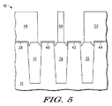
- トレンチを形成する前記工程は、トレンチを、前記第1活性領域と第2活性領域とがトレンチを挟んで対向するように、前記第1活性領域と前記第2活性領域との間に設けることを含み、
前記マスクパターンを形成する工程は、前記トレンチのうち、同トレンチの前記第1側部の反対側に位置する第2側部を露出させることをさらに含み、前記トレンチの前記第2側部は、前記マスクパターンにおける前記第1側部の反対側に位置する第2側部と前記第2活性領域との間に位置しており、
エッチングを行う工程は、前記トレンチの前記第2側部を掘り込むエッチングを行なって、第2窪みを前記トレンチに残すことをさらに含み、
成長させる工程は、第2エピタキシャル領域が前記第2窪みを完全に充填するように前記第2エピタキシャル領域を前記第2窪みに成長させて、前記第2活性領域を延長して前記第2窪みを含むように、第2拡幅活性領域を形成することをさらに含む、請求項1に記載の方法。 - 前記第1拡幅活性領域及び前記第2拡幅活性領域を化学的機械研磨する工程をさらに備える、請求項5に記載の方法。
- 化学的機械研磨する前記工程の後に、前記第1拡幅活性領域及び前記第2活性領域の上を延在し、かつ前記第1エピタキシャル領域及び前記第2エピタキシャル領域の上にも延在するゲートを形成する工程をさらに備える、請求項6に記載の方法。
- 前記マスクパターンを形成する前記工程はさらに、前記マスクパターンがフォトレジストを含むことを特徴とし、前記方法は、エッチングを行う工程の前に、前記フォトレジストをトリミングする工程をさらに備える、請求項7に記載の方法。
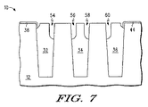
- プレーナ型の半導体素子を形成するために方法において、
半導体基板を設ける工程と、
トレンチを活性領域の周りに、前記活性領域の境界を画定するように形成する工程と、
前記トレンチに絶縁材料を充填して絶縁分離領域を形成する工程と、
マスクパターンが前記活性領域から離間する辺を有することにより、前記絶縁分離領域の露出領域が、前記マスクパターンの前記辺と前記活性領域との間に現われるようにするように、マスクパターンを前記絶縁分離領域の上に形成する工程と、
前記露出領域を掘り込むエッチングを行って窪みを形成する工程と、
前記窪みを完全にふさぐように前記窪みに半導体材料を充填し、該半導体材料をエピタキシャル成長させて、拡幅活性領域を、半導体材料が充填された前記窪みと前記活性領域との合体構造として形成する工程と、
前記拡幅活性領域を化学的機械研磨する工程と、
プレーナ型のトランジスタを前記拡幅活性領域の内部から上方にわたって、チャネルの上に第1方向に延在するゲートを有するように形成する工程とを備え、
前記活性領域は、前記窪みと対応する位置において前記第1方向に延びる第1幅を有し、前記プレーナ型のトランジスタは前記窪みと対応する位置において前記第1幅よりも広いチャネル幅を有する、方法。 - エッチングを行なう工程の前に、前記マスクパターンをトリミングする工程をさらに備える、請求項9に記載の方法。
- 前記ゲートを形成する工程は、前記ゲートが、半導体材料が充填された前記窪みの上を延在することを特徴とする、請求項9に記載の方法。
- 前記マスクパターンを形成する工程は、前記露出領域が、前記活性領域の全周に延在することを特徴とする、請求項9に記載の方法。
- 前記プレーナ型のトランジスタが、半導体材料が充填され、かつ2つの異なる位置に在る前記窪みの上を延在するゲートを有する、請求項9に記載の方法。
Applications Claiming Priority (3)
| Application Number | Priority Date | Filing Date | Title |
|---|---|---|---|
| US12/182,421 US8062953B2 (en) | 2008-07-30 | 2008-07-30 | Semiconductor devices with extended active regions |
| US12/182,421 | 2008-07-30 | ||
| PCT/US2009/043457 WO2010014287A1 (en) | 2008-07-30 | 2009-05-11 | Semiconductor devices with extended active regions |
Publications (3)
| Publication Number | Publication Date |
|---|---|
| JP2011530168A JP2011530168A (ja) | 2011-12-15 |
| JP2011530168A5 JP2011530168A5 (ja) | 2012-07-12 |
| JP5721178B2 true JP5721178B2 (ja) | 2015-05-20 |
Family
ID=41607463
Family Applications (1)
| Application Number | Title | Priority Date | Filing Date |
|---|---|---|---|
| JP2011521138A Active JP5721178B2 (ja) | 2008-07-30 | 2009-05-11 | 拡幅活性領域を有する半導体素子 |
Country Status (5)
| Country | Link |
|---|---|
| US (2) | US8062953B2 (ja) |
| JP (1) | JP5721178B2 (ja) |
| CN (1) | CN102113110B (ja) |
| TW (1) | TW201005874A (ja) |
| WO (1) | WO2010014287A1 (ja) |
Families Citing this family (9)
| Publication number | Priority date | Publication date | Assignee | Title |
|---|---|---|---|---|
| CN103367147A (zh) * | 2012-03-29 | 2013-10-23 | 中芯国际集成电路制造(上海)有限公司 | 一种鳍型半导体器件的制造方法 |
| CN103681325B (zh) * | 2012-09-04 | 2016-08-03 | 中芯国际集成电路制造(上海)有限公司 | 一种鳍片场效应晶体管的制备方法 |
| US9337079B2 (en) * | 2012-10-09 | 2016-05-10 | Stmicroelectronics, Inc. | Prevention of contact to substrate shorts |
| US9437440B2 (en) * | 2012-11-21 | 2016-09-06 | Infineon Technologies Dresden Gmbh | Method for manufacturing a semiconductor device |
| CN104282612B (zh) * | 2013-07-01 | 2017-04-19 | 中芯国际集成电路制造(上海)有限公司 | 一种半导体器件浅沟槽隔离结构的制作方法 |
| TWI562373B (en) * | 2014-02-19 | 2016-12-11 | Vanguard Int Semiconduct Corp | Semiconductor device and method for manufacturing the same |
| US9978861B2 (en) | 2014-04-09 | 2018-05-22 | Vanguard International Semiconductor Corporation | Semiconductor device having gate in trenches |
| BR112016026562A2 (pt) * | 2014-05-15 | 2017-08-15 | Calysta Inc | Métodos para produção biológica de compostos de cadeia de carbono muito longa |
| KR20180096850A (ko) * | 2017-02-20 | 2018-08-30 | 삼성전자주식회사 | 반도체 소자 |
Family Cites Families (11)
| Publication number | Priority date | Publication date | Assignee | Title |
|---|---|---|---|---|
| JP2000260952A (ja) * | 1999-03-05 | 2000-09-22 | Toshiba Corp | 半導体装置 |
| US6483156B1 (en) | 2000-03-16 | 2002-11-19 | International Business Machines Corporation | Double planar gated SOI MOSFET structure |
| JP2002158932A (ja) * | 2000-11-16 | 2002-05-31 | Sony Corp | 固体撮像装置及び固体撮像素子の駆動方法 |
| JP2002270685A (ja) * | 2001-03-08 | 2002-09-20 | Mitsubishi Electric Corp | 半導体装置の製造方法 |
| US6630288B2 (en) * | 2001-03-28 | 2003-10-07 | Advanced Micro Devices, Inc. | Process for forming sub-lithographic photoresist features by modification of the photoresist surface |
| US6716571B2 (en) * | 2001-03-28 | 2004-04-06 | Advanced Micro Devices, Inc. | Selective photoresist hardening to facilitate lateral trimming |
| KR20050045599A (ko) | 2003-11-12 | 2005-05-17 | 삼성전자주식회사 | 선택적 에피텍셜 성장을 이용한 소자분리막 형성방법 |
| KR100673896B1 (ko) * | 2004-07-30 | 2007-01-26 | 주식회사 하이닉스반도체 | 트렌치 구조의 소자분리막을 갖는 반도체소자 및 그 제조방법 |
| JP2006237509A (ja) * | 2005-02-28 | 2006-09-07 | Toshiba Corp | 半導体装置 |
| JP4718894B2 (ja) * | 2005-05-19 | 2011-07-06 | 株式会社東芝 | 半導体装置の製造方法 |
| KR100772114B1 (ko) * | 2006-09-29 | 2007-11-01 | 주식회사 하이닉스반도체 | 반도체 소자의 제조방법 |
-
2008
- 2008-07-30 US US12/182,421 patent/US8062953B2/en active Active
-
2009
- 2009-05-11 JP JP2011521138A patent/JP5721178B2/ja active Active
- 2009-05-11 WO PCT/US2009/043457 patent/WO2010014287A1/en active Application Filing
- 2009-05-11 CN CN2009801297506A patent/CN102113110B/zh active Active
- 2009-05-14 TW TW098116023A patent/TW201005874A/zh unknown
-
2011
- 2011-09-19 US US13/235,580 patent/US20120007155A1/en not_active Abandoned
Also Published As
| Publication number | Publication date |
|---|---|
| US8062953B2 (en) | 2011-11-22 |
| TW201005874A (en) | 2010-02-01 |
| US20120007155A1 (en) | 2012-01-12 |
| CN102113110B (zh) | 2013-12-11 |
| JP2011530168A (ja) | 2011-12-15 |
| WO2010014287A1 (en) | 2010-02-04 |
| US20100025805A1 (en) | 2010-02-04 |
| CN102113110A (zh) | 2011-06-29 |
Similar Documents
| Publication | Publication Date | Title |
|---|---|---|
| JP5721178B2 (ja) | 拡幅活性領域を有する半導体素子 | |
| TWI416634B (zh) | 形成積體電路結構的方法 | |
| US7700456B2 (en) | Semiconductor device and manufacturing method of the same | |
| US7705401B2 (en) | Semiconductor device including a fin-channel recess-gate MISFET | |
| US20130200483A1 (en) | Fin structure and method of forming the same | |
| KR20050035712A (ko) | 핀 전계효과 트랜지스터를 위한 다중 실리콘 핀 및 그형성 방법 | |
| JP2008124423A (ja) | 半導体装置の製造方法及び半導体装置 | |
| JP2007180486A (ja) | 5チャネルのフィントランジスタ及びその製造方法 | |
| JP2013183133A (ja) | 半導体装置の製造方法 | |
| CN108091611B (zh) | 半导体装置及其制造方法 | |
| JP2000031262A (ja) | 半導体装置及びシャロ―・トレンチ・アイソレ―ションの形成方法 | |
| TWI546859B (zh) | 半導體裝置之圖案化結構及其製作方法 | |
| TW201830495A (zh) | 製造半導體裝置的方法 | |
| EP2973680A1 (en) | Spacer enabled poly gate | |
| JP5397402B2 (ja) | 半導体素子の製造方法 | |
| US10978335B2 (en) | Method for producing a gate cut structure on an array of semiconductor fins | |
| US7592208B2 (en) | Method for manufacturing semiconductor substrate and method for manufacturing semiconductor apparatus and photomask | |
| KR101696983B1 (ko) | FinFET 상에 트렌치를 형성하는 방법 및 그 FinFET | |
| JP6281420B2 (ja) | 半導体装置の製造方法 | |
| TW201444086A (zh) | 半導體裝置及其製作方法 | |
| KR100670398B1 (ko) | 수평 방향으로 접혀진 유전막을 포함하는 커패시터 및제조 방법 | |
| KR101059810B1 (ko) | 반도체 소자의 제조방법 | |
| KR101078725B1 (ko) | 반도체 소자 및 그의 제조방법 | |
| KR100714901B1 (ko) | 콘택 구조체의 형성방법들 | |
| JP2000021971A (ja) | 半導体装置の製造方法 |
Legal Events
| Date | Code | Title | Description |
|---|---|---|---|
| RD04 | Notification of resignation of power of attorney |
Free format text: JAPANESE INTERMEDIATE CODE: A7424 Effective date: 20120227 |
|
| A521 | Request for written amendment filed |
Free format text: JAPANESE INTERMEDIATE CODE: A523 Effective date: 20120511 |
|
| A621 | Written request for application examination |
Free format text: JAPANESE INTERMEDIATE CODE: A621 Effective date: 20120511 |
|
| A521 | Request for written amendment filed |
Free format text: JAPANESE INTERMEDIATE CODE: A523 Effective date: 20120523 |
|
| A977 | Report on retrieval |
Free format text: JAPANESE INTERMEDIATE CODE: A971007 Effective date: 20130711 |
|
| A131 | Notification of reasons for refusal |
Free format text: JAPANESE INTERMEDIATE CODE: A131 Effective date: 20130723 |
|
| A601 | Written request for extension of time |
Free format text: JAPANESE INTERMEDIATE CODE: A601 Effective date: 20131022 |
|
| A602 | Written permission of extension of time |
Free format text: JAPANESE INTERMEDIATE CODE: A602 Effective date: 20131029 |
|
| A521 | Request for written amendment filed |
Free format text: JAPANESE INTERMEDIATE CODE: A523 Effective date: 20131030 |
|
| A131 | Notification of reasons for refusal |
Free format text: JAPANESE INTERMEDIATE CODE: A131 Effective date: 20140507 |
|
| A521 | Request for written amendment filed |
Free format text: JAPANESE INTERMEDIATE CODE: A523 Effective date: 20140709 |
|
| TRDD | Decision of grant or rejection written | ||
| A01 | Written decision to grant a patent or to grant a registration (utility model) |
Free format text: JAPANESE INTERMEDIATE CODE: A01 Effective date: 20150224 |
|
| A61 | First payment of annual fees (during grant procedure) |
Free format text: JAPANESE INTERMEDIATE CODE: A61 Effective date: 20150319 |
|
| R150 | Certificate of patent or registration of utility model |
Ref document number: 5721178 Country of ref document: JP Free format text: JAPANESE INTERMEDIATE CODE: R150 |
|
| S533 | Written request for registration of change of name |
Free format text: JAPANESE INTERMEDIATE CODE: R313533 |
|
| R350 | Written notification of registration of transfer |
Free format text: JAPANESE INTERMEDIATE CODE: R350 |
|
| R250 | Receipt of annual fees |
Free format text: JAPANESE INTERMEDIATE CODE: R250 |
|
| R250 | Receipt of annual fees |
Free format text: JAPANESE INTERMEDIATE CODE: R250 |
|
| R250 | Receipt of annual fees |
Free format text: JAPANESE INTERMEDIATE CODE: R250 |
|
| R250 | Receipt of annual fees |
Free format text: JAPANESE INTERMEDIATE CODE: R250 |
|
| R250 | Receipt of annual fees |
Free format text: JAPANESE INTERMEDIATE CODE: R250 |
|
| R250 | Receipt of annual fees |
Free format text: JAPANESE INTERMEDIATE CODE: R250 |
|
| R250 | Receipt of annual fees |
Free format text: JAPANESE INTERMEDIATE CODE: R250 |