JP5063114B2 - プレーナ型ハイブリッド配向基板を形成する方法 - Google Patents
プレーナ型ハイブリッド配向基板を形成する方法 Download PDFInfo
- Publication number
- JP5063114B2 JP5063114B2 JP2006542666A JP2006542666A JP5063114B2 JP 5063114 B2 JP5063114 B2 JP 5063114B2 JP 2006542666 A JP2006542666 A JP 2006542666A JP 2006542666 A JP2006542666 A JP 2006542666A JP 5063114 B2 JP5063114 B2 JP 5063114B2
- Authority
- JP
- Japan
- Prior art keywords
- single crystal
- layer
- crystal semiconductor
- region
- semiconductor layer
- Prior art date
- Legal status (The legal status is an assumption and is not a legal conclusion. Google has not performed a legal analysis and makes no representation as to the accuracy of the status listed.)
- Expired - Fee Related
Links
- 239000000758 substrate Substances 0.000 title claims description 125
- 238000000034 method Methods 0.000 title claims description 87
- 239000004065 semiconductor Substances 0.000 claims description 145
- 239000013078 crystal Substances 0.000 claims description 93
- 238000002955 isolation Methods 0.000 claims description 22
- 238000001953 recrystallisation Methods 0.000 claims description 19
- 238000005280 amorphization Methods 0.000 claims description 17
- 239000000463 material Substances 0.000 claims description 11
- 238000005468 ion implantation Methods 0.000 claims description 9
- 229910052760 oxygen Inorganic materials 0.000 claims description 8
- QVGXLLKOCUKJST-UHFFFAOYSA-N atomic oxygen Chemical compound [O] QVGXLLKOCUKJST-UHFFFAOYSA-N 0.000 claims description 6
- 239000001301 oxygen Substances 0.000 claims description 6
- 150000002500 ions Chemical class 0.000 claims description 5
- 229910052710 silicon Inorganic materials 0.000 claims description 5
- 229910052734 helium Inorganic materials 0.000 claims description 4
- 229910052739 hydrogen Inorganic materials 0.000 claims description 4
- 229910052757 nitrogen Inorganic materials 0.000 claims description 4
- 229910000577 Silicon-germanium Inorganic materials 0.000 claims description 3
- 229910045601 alloy Inorganic materials 0.000 claims description 3
- 239000000956 alloy Substances 0.000 claims description 3
- 229910052786 argon Inorganic materials 0.000 claims description 3
- 239000007789 gas Substances 0.000 claims description 3
- 229910052732 germanium Inorganic materials 0.000 claims description 3
- 238000000926 separation method Methods 0.000 claims description 3
- 229910001218 Gallium arsenide Inorganic materials 0.000 claims description 2
- 229910000673 Indium arsenide Inorganic materials 0.000 claims description 2
- 229910003811 SiGeC Inorganic materials 0.000 claims description 2
- 229910052785 arsenic Inorganic materials 0.000 claims description 2
- 229910052796 boron Inorganic materials 0.000 claims description 2
- 229910052799 carbon Inorganic materials 0.000 claims description 2
- 150000001875 compounds Chemical class 0.000 claims description 2
- RPQDHPTXJYYUPQ-UHFFFAOYSA-N indium arsenide Chemical compound [In]#[As] RPQDHPTXJYYUPQ-UHFFFAOYSA-N 0.000 claims description 2
- 229910052743 krypton Inorganic materials 0.000 claims description 2
- 239000000203 mixture Substances 0.000 claims description 2
- 229910003465 moissanite Inorganic materials 0.000 claims description 2
- 229910010271 silicon carbide Inorganic materials 0.000 claims description 2
- 229910000927 Ge alloy Inorganic materials 0.000 claims 1
- 238000004519 manufacturing process Methods 0.000 description 16
- 229910021421 monocrystalline silicon Inorganic materials 0.000 description 14
- 238000000137 annealing Methods 0.000 description 8
- 238000002513 implantation Methods 0.000 description 7
- 238000010849 ion bombardment Methods 0.000 description 6
- 239000012535 impurity Substances 0.000 description 3
- 230000004048 modification Effects 0.000 description 3
- 238000012986 modification Methods 0.000 description 3
- 238000005498 polishing Methods 0.000 description 3
- IJGRMHOSHXDMSA-UHFFFAOYSA-N Atomic nitrogen Chemical compound N#N IJGRMHOSHXDMSA-UHFFFAOYSA-N 0.000 description 2
- 229910004298 SiO 2 Inorganic materials 0.000 description 2
- 230000015572 biosynthetic process Effects 0.000 description 2
- 239000012212 insulator Substances 0.000 description 2
- 229910044991 metal oxide Inorganic materials 0.000 description 2
- 150000004706 metal oxides Chemical class 0.000 description 2
- 238000001020 plasma etching Methods 0.000 description 2
- 230000001681 protective effect Effects 0.000 description 2
- 125000006850 spacer group Chemical group 0.000 description 2
- 229910018072 Al 2 O 3 Inorganic materials 0.000 description 1
- 108091006149 Electron carriers Proteins 0.000 description 1
- 229910052581 Si3N4 Inorganic materials 0.000 description 1
- 239000000969 carrier Substances 0.000 description 1
- 230000000295 complement effect Effects 0.000 description 1
- 239000004020 conductor Substances 0.000 description 1
- 229910021488 crystalline silicon dioxide Inorganic materials 0.000 description 1
- 230000007547 defect Effects 0.000 description 1
- 238000000151 deposition Methods 0.000 description 1
- 229910003460 diamond Inorganic materials 0.000 description 1
- 239000010432 diamond Substances 0.000 description 1
- 239000003989 dielectric material Substances 0.000 description 1
- 239000002019 doping agent Substances 0.000 description 1
- 238000005530 etching Methods 0.000 description 1
- 230000005669 field effect Effects 0.000 description 1
- 238000000227 grinding Methods 0.000 description 1
- 230000002209 hydrophobic effect Effects 0.000 description 1
- 239000011810 insulating material Substances 0.000 description 1
- 238000005224 laser annealing Methods 0.000 description 1
- 239000002184 metal Substances 0.000 description 1
- 229910052751 metal Inorganic materials 0.000 description 1
- 150000004767 nitrides Chemical class 0.000 description 1
- 230000003647 oxidation Effects 0.000 description 1
- 238000007254 oxidation reaction Methods 0.000 description 1
- 229920002120 photoresistant polymer Polymers 0.000 description 1
- 229910021420 polycrystalline silicon Inorganic materials 0.000 description 1
- 229910021426 porous silicon Inorganic materials 0.000 description 1
- 238000004151 rapid thermal annealing Methods 0.000 description 1
- 239000010703 silicon Substances 0.000 description 1
- HQVNEWCFYHHQES-UHFFFAOYSA-N silicon nitride Chemical compound N12[Si]34N5[Si]62N3[Si]51N64 HQVNEWCFYHHQES-UHFFFAOYSA-N 0.000 description 1
- 239000007787 solid Substances 0.000 description 1
- 238000006467 substitution reaction Methods 0.000 description 1
- 238000009279 wet oxidation reaction Methods 0.000 description 1
Images


Classifications
-
- H—ELECTRICITY
- H01—ELECTRIC ELEMENTS
- H01L—SEMICONDUCTOR DEVICES NOT COVERED BY CLASS H10
- H01L21/00—Processes or apparatus adapted for the manufacture or treatment of semiconductor or solid state devices or of parts thereof
- H01L21/70—Manufacture or treatment of devices consisting of a plurality of solid state components formed in or on a common substrate or of parts thereof; Manufacture of integrated circuit devices or of parts thereof
- H01L21/71—Manufacture of specific parts of devices defined in group H01L21/70
- H01L21/76—Making of isolation regions between components
- H01L21/762—Dielectric regions, e.g. EPIC dielectric isolation, LOCOS; Trench refilling techniques, SOI technology, use of channel stoppers
- H01L21/7624—Dielectric regions, e.g. EPIC dielectric isolation, LOCOS; Trench refilling techniques, SOI technology, use of channel stoppers using semiconductor on insulator [SOI] technology
- H01L21/76251—Dielectric regions, e.g. EPIC dielectric isolation, LOCOS; Trench refilling techniques, SOI technology, use of channel stoppers using semiconductor on insulator [SOI] technology using bonding techniques
-
- H—ELECTRICITY
- H01—ELECTRIC ELEMENTS
- H01L—SEMICONDUCTOR DEVICES NOT COVERED BY CLASS H10
- H01L27/00—Devices consisting of a plurality of semiconductor or other solid-state components formed in or on a common substrate
- H01L27/02—Devices consisting of a plurality of semiconductor or other solid-state components formed in or on a common substrate including semiconductor components specially adapted for rectifying, oscillating, amplifying or switching and having at least one potential-jump barrier or surface barrier; including integrated passive circuit elements with at least one potential-jump barrier or surface barrier
- H01L27/12—Devices consisting of a plurality of semiconductor or other solid-state components formed in or on a common substrate including semiconductor components specially adapted for rectifying, oscillating, amplifying or switching and having at least one potential-jump barrier or surface barrier; including integrated passive circuit elements with at least one potential-jump barrier or surface barrier the substrate being other than a semiconductor body, e.g. an insulating body
-
- H—ELECTRICITY
- H01—ELECTRIC ELEMENTS
- H01L—SEMICONDUCTOR DEVICES NOT COVERED BY CLASS H10
- H01L21/00—Processes or apparatus adapted for the manufacture or treatment of semiconductor or solid state devices or of parts thereof
- H01L21/02—Manufacture or treatment of semiconductor devices or of parts thereof
- H01L21/02104—Forming layers
- H01L21/02365—Forming inorganic semiconducting materials on a substrate
- H01L21/02518—Deposited layers
- H01L21/02609—Crystal orientation
-
- H—ELECTRICITY
- H01—ELECTRIC ELEMENTS
- H01L—SEMICONDUCTOR DEVICES NOT COVERED BY CLASS H10
- H01L21/00—Processes or apparatus adapted for the manufacture or treatment of semiconductor or solid state devices or of parts thereof
- H01L21/02—Manufacture or treatment of semiconductor devices or of parts thereof
- H01L21/02104—Forming layers
- H01L21/02365—Forming inorganic semiconducting materials on a substrate
- H01L21/02656—Special treatments
- H01L21/02664—Aftertreatments
- H01L21/02667—Crystallisation or recrystallisation of non-monocrystalline semiconductor materials, e.g. regrowth
-
- H—ELECTRICITY
- H01—ELECTRIC ELEMENTS
- H01L—SEMICONDUCTOR DEVICES NOT COVERED BY CLASS H10
- H01L21/00—Processes or apparatus adapted for the manufacture or treatment of semiconductor or solid state devices or of parts thereof
- H01L21/70—Manufacture or treatment of devices consisting of a plurality of solid state components formed in or on a common substrate or of parts thereof; Manufacture of integrated circuit devices or of parts thereof
- H01L21/71—Manufacture of specific parts of devices defined in group H01L21/70
- H01L21/76—Making of isolation regions between components
- H01L21/762—Dielectric regions, e.g. EPIC dielectric isolation, LOCOS; Trench refilling techniques, SOI technology, use of channel stoppers
- H01L21/7624—Dielectric regions, e.g. EPIC dielectric isolation, LOCOS; Trench refilling techniques, SOI technology, use of channel stoppers using semiconductor on insulator [SOI] technology
- H01L21/76264—SOI together with lateral isolation, e.g. using local oxidation of silicon, or dielectric or polycristalline material refilled trench or air gap isolation regions, e.g. completely isolated semiconductor islands
- H01L21/76275—Vertical isolation by bonding techniques
-
- H—ELECTRICITY
- H01—ELECTRIC ELEMENTS
- H01L—SEMICONDUCTOR DEVICES NOT COVERED BY CLASS H10
- H01L21/00—Processes or apparatus adapted for the manufacture or treatment of semiconductor or solid state devices or of parts thereof
- H01L21/70—Manufacture or treatment of devices consisting of a plurality of solid state components formed in or on a common substrate or of parts thereof; Manufacture of integrated circuit devices or of parts thereof
- H01L21/77—Manufacture or treatment of devices consisting of a plurality of solid state components or integrated circuits formed in, or on, a common substrate
- H01L21/78—Manufacture or treatment of devices consisting of a plurality of solid state components or integrated circuits formed in, or on, a common substrate with subsequent division of the substrate into plural individual devices
- H01L21/82—Manufacture or treatment of devices consisting of a plurality of solid state components or integrated circuits formed in, or on, a common substrate with subsequent division of the substrate into plural individual devices to produce devices, e.g. integrated circuits, each consisting of a plurality of components
- H01L21/822—Manufacture or treatment of devices consisting of a plurality of solid state components or integrated circuits formed in, or on, a common substrate with subsequent division of the substrate into plural individual devices to produce devices, e.g. integrated circuits, each consisting of a plurality of components the substrate being a semiconductor, using silicon technology
- H01L21/8232—Field-effect technology
- H01L21/8234—MIS technology, i.e. integration processes of field effect transistors of the conductor-insulator-semiconductor type
- H01L21/8238—Complementary field-effect transistors, e.g. CMOS
- H01L21/823807—Complementary field-effect transistors, e.g. CMOS with a particular manufacturing method of the channel structures, e.g. channel implants, halo or pocket implants, or channel materials
-
- H—ELECTRICITY
- H01—ELECTRIC ELEMENTS
- H01L—SEMICONDUCTOR DEVICES NOT COVERED BY CLASS H10
- H01L21/00—Processes or apparatus adapted for the manufacture or treatment of semiconductor or solid state devices or of parts thereof
- H01L21/70—Manufacture or treatment of devices consisting of a plurality of solid state components formed in or on a common substrate or of parts thereof; Manufacture of integrated circuit devices or of parts thereof
- H01L21/77—Manufacture or treatment of devices consisting of a plurality of solid state components or integrated circuits formed in, or on, a common substrate
- H01L21/78—Manufacture or treatment of devices consisting of a plurality of solid state components or integrated circuits formed in, or on, a common substrate with subsequent division of the substrate into plural individual devices
- H01L21/82—Manufacture or treatment of devices consisting of a plurality of solid state components or integrated circuits formed in, or on, a common substrate with subsequent division of the substrate into plural individual devices to produce devices, e.g. integrated circuits, each consisting of a plurality of components
- H01L21/84—Manufacture or treatment of devices consisting of a plurality of solid state components or integrated circuits formed in, or on, a common substrate with subsequent division of the substrate into plural individual devices to produce devices, e.g. integrated circuits, each consisting of a plurality of components the substrate being other than a semiconductor body, e.g. being an insulating body
-
- H—ELECTRICITY
- H01—ELECTRIC ELEMENTS
- H01L—SEMICONDUCTOR DEVICES NOT COVERED BY CLASS H10
- H01L27/00—Devices consisting of a plurality of semiconductor or other solid-state components formed in or on a common substrate
- H01L27/02—Devices consisting of a plurality of semiconductor or other solid-state components formed in or on a common substrate including semiconductor components specially adapted for rectifying, oscillating, amplifying or switching and having at least one potential-jump barrier or surface barrier; including integrated passive circuit elements with at least one potential-jump barrier or surface barrier
- H01L27/12—Devices consisting of a plurality of semiconductor or other solid-state components formed in or on a common substrate including semiconductor components specially adapted for rectifying, oscillating, amplifying or switching and having at least one potential-jump barrier or surface barrier; including integrated passive circuit elements with at least one potential-jump barrier or surface barrier the substrate being other than a semiconductor body, e.g. an insulating body
- H01L27/1203—Devices consisting of a plurality of semiconductor or other solid-state components formed in or on a common substrate including semiconductor components specially adapted for rectifying, oscillating, amplifying or switching and having at least one potential-jump barrier or surface barrier; including integrated passive circuit elements with at least one potential-jump barrier or surface barrier the substrate being other than a semiconductor body, e.g. an insulating body the substrate comprising an insulating body on a semiconductor body, e.g. SOI
- H01L27/1207—Devices consisting of a plurality of semiconductor or other solid-state components formed in or on a common substrate including semiconductor components specially adapted for rectifying, oscillating, amplifying or switching and having at least one potential-jump barrier or surface barrier; including integrated passive circuit elements with at least one potential-jump barrier or surface barrier the substrate being other than a semiconductor body, e.g. an insulating body the substrate comprising an insulating body on a semiconductor body, e.g. SOI combined with devices in contact with the semiconductor body, i.e. bulk/SOI hybrid circuits
-
- H—ELECTRICITY
- H01—ELECTRIC ELEMENTS
- H01L—SEMICONDUCTOR DEVICES NOT COVERED BY CLASS H10
- H01L29/00—Semiconductor devices adapted for rectifying, amplifying, oscillating or switching, or capacitors or resistors with at least one potential-jump barrier or surface barrier, e.g. PN junction depletion layer or carrier concentration layer; Details of semiconductor bodies or of electrodes thereof ; Multistep manufacturing processes therefor
- H01L29/02—Semiconductor bodies ; Multistep manufacturing processes therefor
- H01L29/04—Semiconductor bodies ; Multistep manufacturing processes therefor characterised by their crystalline structure, e.g. polycrystalline, cubic or particular orientation of crystalline planes
- H01L29/045—Semiconductor bodies ; Multistep manufacturing processes therefor characterised by their crystalline structure, e.g. polycrystalline, cubic or particular orientation of crystalline planes by their particular orientation of crystalline planes
-
- H—ELECTRICITY
- H01—ELECTRIC ELEMENTS
- H01L—SEMICONDUCTOR DEVICES NOT COVERED BY CLASS H10
- H01L29/00—Semiconductor devices adapted for rectifying, amplifying, oscillating or switching, or capacitors or resistors with at least one potential-jump barrier or surface barrier, e.g. PN junction depletion layer or carrier concentration layer; Details of semiconductor bodies or of electrodes thereof ; Multistep manufacturing processes therefor
- H01L29/02—Semiconductor bodies ; Multistep manufacturing processes therefor
- H01L29/06—Semiconductor bodies ; Multistep manufacturing processes therefor characterised by their shape; characterised by the shapes, relative sizes, or dispositions of the semiconductor regions ; characterised by the concentration or distribution of impurities within semiconductor regions
- H01L29/10—Semiconductor bodies ; Multistep manufacturing processes therefor characterised by their shape; characterised by the shapes, relative sizes, or dispositions of the semiconductor regions ; characterised by the concentration or distribution of impurities within semiconductor regions with semiconductor regions connected to an electrode not carrying current to be rectified, amplified or switched and such electrode being part of a semiconductor device which comprises three or more electrodes
- H01L29/1025—Channel region of field-effect devices
- H01L29/1029—Channel region of field-effect devices of field-effect transistors
- H01L29/1033—Channel region of field-effect devices of field-effect transistors with insulated gate, e.g. characterised by the length, the width, the geometric contour or the doping structure
- H01L29/1054—Channel region of field-effect devices of field-effect transistors with insulated gate, e.g. characterised by the length, the width, the geometric contour or the doping structure with a variation of the composition, e.g. channel with strained layer for increasing the mobility
-
- H—ELECTRICITY
- H01—ELECTRIC ELEMENTS
- H01L—SEMICONDUCTOR DEVICES NOT COVERED BY CLASS H10
- H01L29/00—Semiconductor devices adapted for rectifying, amplifying, oscillating or switching, or capacitors or resistors with at least one potential-jump barrier or surface barrier, e.g. PN junction depletion layer or carrier concentration layer; Details of semiconductor bodies or of electrodes thereof ; Multistep manufacturing processes therefor
- H01L29/66—Types of semiconductor device ; Multistep manufacturing processes therefor
- H01L29/66007—Multistep manufacturing processes
- H01L29/66075—Multistep manufacturing processes of devices having semiconductor bodies comprising group 14 or group 13/15 materials
- H01L29/66227—Multistep manufacturing processes of devices having semiconductor bodies comprising group 14 or group 13/15 materials the devices being controllable only by the electric current supplied or the electric potential applied, to an electrode which does not carry the current to be rectified, amplified or switched, e.g. three-terminal devices
- H01L29/66409—Unipolar field-effect transistors
- H01L29/66477—Unipolar field-effect transistors with an insulated gate, i.e. MISFET
- H01L29/66742—Thin film unipolar transistors
- H01L29/66772—Monocristalline silicon transistors on insulating substrates, e.g. quartz substrates
-
- H—ELECTRICITY
- H01—ELECTRIC ELEMENTS
- H01L—SEMICONDUCTOR DEVICES NOT COVERED BY CLASS H10
- H01L29/00—Semiconductor devices adapted for rectifying, amplifying, oscillating or switching, or capacitors or resistors with at least one potential-jump barrier or surface barrier, e.g. PN junction depletion layer or carrier concentration layer; Details of semiconductor bodies or of electrodes thereof ; Multistep manufacturing processes therefor
- H01L29/66—Types of semiconductor device ; Multistep manufacturing processes therefor
- H01L29/68—Types of semiconductor device ; Multistep manufacturing processes therefor controllable by only the electric current supplied, or only the electric potential applied, to an electrode which does not carry the current to be rectified, amplified or switched
- H01L29/76—Unipolar devices, e.g. field effect transistors
- H01L29/772—Field effect transistors
- H01L29/78—Field effect transistors with field effect produced by an insulated gate
- H01L29/786—Thin film transistors, i.e. transistors with a channel being at least partly a thin film
- H01L29/78651—Silicon transistors
- H01L29/78654—Monocrystalline silicon transistors
-
- H—ELECTRICITY
- H01—ELECTRIC ELEMENTS
- H01L—SEMICONDUCTOR DEVICES NOT COVERED BY CLASS H10
- H01L29/00—Semiconductor devices adapted for rectifying, amplifying, oscillating or switching, or capacitors or resistors with at least one potential-jump barrier or surface barrier, e.g. PN junction depletion layer or carrier concentration layer; Details of semiconductor bodies or of electrodes thereof ; Multistep manufacturing processes therefor
- H01L29/66—Types of semiconductor device ; Multistep manufacturing processes therefor
- H01L29/68—Types of semiconductor device ; Multistep manufacturing processes therefor controllable by only the electric current supplied, or only the electric potential applied, to an electrode which does not carry the current to be rectified, amplified or switched
- H01L29/76—Unipolar devices, e.g. field effect transistors
- H01L29/772—Field effect transistors
- H01L29/78—Field effect transistors with field effect produced by an insulated gate
- H01L29/786—Thin film transistors, i.e. transistors with a channel being at least partly a thin film
- H01L29/78696—Thin film transistors, i.e. transistors with a channel being at least partly a thin film characterised by the structure of the channel, e.g. multichannel, transverse or longitudinal shape, length or width, doping structure, or the overlap or alignment between the channel and the gate, the source or the drain, or the contacting structure of the channel
Description
第1の配向を有する第1の下部単結晶半導体層(又は基板)と、第1の配向とは異なる第2の配向を有する第2の上部(一般的には、接合された)単結晶半導体層とからなる二層テンプレート層スタックを形成するステップ、
選択された領域において二層テンプレート・スタックの層の一方をアモルファス化し(例えば、マスクを通してイオン注入によって)、局部的なアモルファス化領域を形成するステップ、及び
テンプレートとしてアモルファス化されていないスタックの層を用いて、局部的なアモルファス化領域を再結晶化し、これにより該局部的なアモルファス化領域の配向を元の配向から所望の配向に変えるステップである。
第1の配向を有する第1の下部単結晶半導体層(又は基板)と、第1の配向とは異なる第2の配向を有する第2の上部(一般的には、接合された)単結晶半導体層からなる二層テンプレート層スタックを形成するステップ、
選択された領域において二層テンプレート・スタックの層の一方をアモルファス化し、局部的なアモルファス化領域を形成するステップ、及び
テンプレートとしてアモルファス化されていないスタックの層を用いて、局部的なアモルファス化領域を再結晶化し、これにより該局部的なアモルファス化領域の配向を元の配向から所望の配向に変えるステップである。
Claims (17)
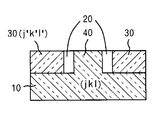
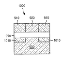
- プレーナ型ハイブリッド配向基板を形成する方法であって、
埋め込み絶縁層上に形成され第1の結晶配向を有する第1の下部単結晶半導体層、及び該第1の下部単結晶半導体層の上に形成され前記第1の結晶配向と異なる第2の結晶配向を有する第2の上部単結晶半導体層を有する二層テンプレート・スタックを準備するステップと、
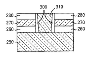
前記埋込み絶縁層から前記第1の下部単結晶半導体層を通り前記第2の上部単結晶半導体層内に部分的に延びる局部的なアモルファス化領域を形成するように、前記第1の下部単結晶半導体層の一部と前記第2の上部単結晶半導体層の一部とをアモルファス化するステップと、
前記第2の上部単結晶半導体層をテンプレートとして使用して前記局部的なアモルファス化領域を再結晶化することにより、前記第2の上部単結晶半導体層の前記第2の結晶配向を有する単結晶半導体領域を形成するステップと、
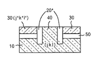
前記第2の上部単結晶半導体層を除去して、同一平面の前記第1の下部単結晶半導体層及び前記単結晶半導体領域を残すステップとを含む方法。 - 前記第2の上部単結晶半導体層が、接合によって前記第1の下部単結晶半導体の上に形成される、請求項1に記載の方法。
- 前記アモルファス化するステップの前に、
前記局部的なアモルファス化領域を形成するための少なくとも前記第2の上部単結晶半導体層の一部と該一部に隣接する残りの部分との間に、トレンチ分離領域を形成するステップを行う、請求項1に記載の方法。 - 前記アモルファス化するステップと前記単結晶半導体領域を形成するステップの間に、
前記局部的なアモルファス化領域と該局部的なアモルファス化領域に隣接する部分との間に、トレンチ分離領域を形成するステップを行う、請求項1に記載の方法。 - 前記アモルファス化するステップの後に、前記局部的なアモルファス化領域と該局部的なアモルファス化領域に隣接する部分との間に、トレンチ分離領域のトレンチを形成するステップを行い、
前記単結晶半導体領域を形成するステップの後に前記トレンチを充填して前記トレンチ分離領域を形成するステップを行う、請求項1に記載の方法。 - 前記二層テンプレート・スタックは、基板上に形成される、請求項1に記載の方法。
- 前記第1の下部単結晶半導体層及び前記第2の上部単結晶半導体層は、Si、SiC、SiGe、SiGeC、Ge合金、Ge、C、GaAs、InAs、InP、これらの層状の組み合わせ又はこれらの合金、及び、他のIII−V族又はII−VI族化合物半導体からなる群から選択された同じ半導体材料又は異なる半導体材料から構成される、請求項1に記載の方法。
- 前記第1の下部単結晶半導体層及び前記第2の上部単結晶半導体層の両方が、Si半導体材料から構成される、請求項1に記載の方法。
- 前記第1の下部単結晶半導体層及び前記第2の上部単結晶半導体層が、歪み半導体材料、非歪み半導体材料、又は歪み半導体材料と非歪み半導体材料の組み合わせから構成される、請求項1に記載の方法。
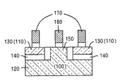
- 前記第1の下部単結晶半導体層及び前記第2の上部単結晶半導体層が、(110)、(111)、及び(100)から選択される異なる結晶配向を有する、請求項1に記載の方法。
- 前記第1の下部単結晶半導体層の前記第1の結晶配向が(100)であり、前記単結晶半導体領域の前記第2の結晶配向が(110)であり、前記第1の下部単結晶半導体層にnFETを形成し、前記単結晶半導体領域にpFETを形成するステップを含む、請求項1に記載の方法。
- 前記第1の下部単結晶半導体層の前記第1の結晶配向が(110)であり、前記単結晶半導体領域の前記第2の結晶配向が(100)であり、前記第1の下部単結晶半導体層にpFETを形成し、前記単結晶半導体領域にnFETを形成するステップを含む、請求項1に記載の方法。
- 前記埋め込み絶縁層は、酸素のイオン注入による分離(SIMOX)プロセスによって形成される、請求項1に記載の方法。
- 前記アモルファス化するステップは、イオン注入によって達成される、請求項1に記載の方法。
- 前記イオン注入は、Si、Ge、Ar、C、O、N、H、He、Kr、Xe、P、B、及びAsからなる群から選択されるイオンを含む、請求項14に記載の方法。
- 前記再結晶化するステップが、200℃から1300℃までの温度で行われる、請求項1に記載の方法。
- 前記再結晶化するステップは、N2、Ar、He、H2、及びこれらの混合物からなる群から選択されるガス内で行われる、請求項1に記載の方法。
Applications Claiming Priority (3)
| Application Number | Priority Date | Filing Date | Title |
|---|---|---|---|
| US10/725,850 | 2003-12-02 | ||
| US10/725,850 US20050116290A1 (en) | 2003-12-02 | 2003-12-02 | Planar substrate with selected semiconductor crystal orientations formed by localized amorphization and recrystallization of stacked template layers |
| PCT/US2004/039970 WO2005057631A2 (en) | 2003-12-02 | 2004-11-30 | Planar substrate with selected semiconductor crystal orientations formed by localized amorphzation and recrystallization of stacked template layers |
Publications (3)
| Publication Number | Publication Date |
|---|---|
| JP2007535802A JP2007535802A (ja) | 2007-12-06 |
| JP2007535802A5 JP2007535802A5 (ja) | 2008-01-24 |
| JP5063114B2 true JP5063114B2 (ja) | 2012-10-31 |
Family
ID=34620372
Family Applications (1)
| Application Number | Title | Priority Date | Filing Date |
|---|---|---|---|
| JP2006542666A Expired - Fee Related JP5063114B2 (ja) | 2003-12-02 | 2004-11-30 | プレーナ型ハイブリッド配向基板を形成する方法 |
Country Status (7)
| Country | Link |
|---|---|
| US (2) | US20050116290A1 (ja) |
| EP (1) | EP1702350A2 (ja) |
| JP (1) | JP5063114B2 (ja) |
| KR (1) | KR100961800B1 (ja) |
| CN (1) | CN100505273C (ja) |
| TW (1) | TWI328286B (ja) |
| WO (1) | WO2005057631A2 (ja) |
Families Citing this family (124)
| Publication number | Priority date | Publication date | Assignee | Title |
|---|---|---|---|---|
| JP2004119943A (ja) * | 2002-09-30 | 2004-04-15 | Renesas Technology Corp | 半導体ウェハおよびその製造方法 |
| US20050116290A1 (en) | 2003-12-02 | 2005-06-02 | De Souza Joel P. | Planar substrate with selected semiconductor crystal orientations formed by localized amorphization and recrystallization of stacked template layers |
| US7291886B2 (en) * | 2004-06-21 | 2007-11-06 | International Business Machines Corporation | Hybrid substrate technology for high-mobility planar and multiple-gate MOSFETs |
| US7253034B2 (en) * | 2004-07-29 | 2007-08-07 | International Business Machines Corporation | Dual SIMOX hybrid orientation technology (HOT) substrates |
| US7354806B2 (en) * | 2004-09-17 | 2008-04-08 | International Business Machines Corporation | Semiconductor device structure with active regions having different surface directions and methods |
| US7235433B2 (en) * | 2004-11-01 | 2007-06-26 | Advanced Micro Devices, Inc. | Silicon-on-insulator semiconductor device with silicon layers having different crystal orientations and method of forming the silicon-on-insulator semiconductor device |
| DE102004057764B4 (de) * | 2004-11-30 | 2013-05-16 | Advanced Micro Devices, Inc. | Verfahren zur Herstellung eines Substrats mit kristallinen Halbleitergebieten mit unterschiedlichen Eigenschaften, die über einem kristallinen Vollsubstrat angeordnet sind und damit hergestelltes Halbleiterbauelement |
| US7393733B2 (en) * | 2004-12-01 | 2008-07-01 | Amberwave Systems Corporation | Methods of forming hybrid fin field-effect transistor structures |
| US7422956B2 (en) * | 2004-12-08 | 2008-09-09 | Advanced Micro Devices, Inc. | Semiconductor device and method of making semiconductor device comprising multiple stacked hybrid orientation layers |
| US7285473B2 (en) * | 2005-01-07 | 2007-10-23 | International Business Machines Corporation | Method for fabricating low-defect-density changed orientation Si |
| US8138061B2 (en) * | 2005-01-07 | 2012-03-20 | International Business Machines Corporation | Quasi-hydrophobic Si-Si wafer bonding using hydrophilic Si surfaces and dissolution of interfacial bonding oxide |
| US20060175659A1 (en) * | 2005-02-07 | 2006-08-10 | International Business Machines Corporation | A cmos structure for body ties in ultra-thin soi (utsoi) substrates |
| US7547917B2 (en) * | 2005-04-06 | 2009-06-16 | International Business Machines Corporation | Inverted multilayer semiconductor device assembly |
| US7250351B2 (en) * | 2005-04-14 | 2007-07-31 | International Business Machines Corporation | Enhanced silicon-on-insulator (SOI) transistors and methods of making enhanced SOI transistors |
| US7291539B2 (en) * | 2005-06-01 | 2007-11-06 | International Business Machines Corporation | Amorphization/templated recrystallization method for hybrid orientation substrates |
| US7358164B2 (en) * | 2005-06-16 | 2008-04-15 | International Business Machines Corporation | Crystal imprinting methods for fabricating substrates with thin active silicon layers |
| US7439108B2 (en) * | 2005-06-16 | 2008-10-21 | International Business Machines Corporation | Coplanar silicon-on-insulator (SOI) regions of different crystal orientations and methods of making the same |
| US7473985B2 (en) * | 2005-06-16 | 2009-01-06 | International Business Machines Corporation | Hybrid oriented substrates and crystal imprinting methods for forming such hybrid oriented substrates |
| US7344962B2 (en) * | 2005-06-21 | 2008-03-18 | International Business Machines Corporation | Method of manufacturing dual orientation wafers |
| US7217629B2 (en) * | 2005-07-15 | 2007-05-15 | International Business Machines Corporation | Epitaxial imprinting |
| US20070040235A1 (en) * | 2005-08-19 | 2007-02-22 | International Business Machines Corporation | Dual trench isolation for CMOS with hybrid orientations |
| DE102005052055B3 (de) | 2005-10-31 | 2007-04-26 | Advanced Micro Devices, Inc., Sunnyvale | Eingebettete Verformungsschicht in dünnen SOI-Transistoren und Verfahren zur Herstellung desselben |
| WO2007053382A1 (en) * | 2005-10-31 | 2007-05-10 | Advanced Micro Devices, Inc. | An embedded strain layer in thin soi transistors and a method of forming the same |
| US8120060B2 (en) * | 2005-11-01 | 2012-02-21 | Massachusetts Institute Of Technology | Monolithically integrated silicon and III-V electronics |
| US7986029B2 (en) * | 2005-11-08 | 2011-07-26 | Taiwan Semiconductor Manufacturing Company, Ltd. | Dual SOI structure |
| US7288458B2 (en) * | 2005-12-14 | 2007-10-30 | Freescale Semiconductor, Inc. | SOI active layer with different surface orientation |
| US7569466B2 (en) * | 2005-12-16 | 2009-08-04 | International Business Machines Corporation | Dual metal gate self-aligned integration |
| US7436034B2 (en) * | 2005-12-19 | 2008-10-14 | International Business Machines Corporation | Metal oxynitride as a pFET material |
| US8319285B2 (en) * | 2005-12-22 | 2012-11-27 | Infineon Technologies Ag | Silicon-on-insulator chip having multiple crystal orientations |
| US8530355B2 (en) * | 2005-12-23 | 2013-09-10 | Infineon Technologies Ag | Mixed orientation semiconductor device and method |
| US7432567B2 (en) * | 2005-12-28 | 2008-10-07 | International Business Machines Corporation | Metal gate CMOS with at least a single gate metal and dual gate dielectrics |
| US7833849B2 (en) | 2005-12-30 | 2010-11-16 | International Business Machines Corporation | Method of fabricating a semiconductor structure including one device region having a metal gate electrode located atop a thinned polygate electrode |
| US7425497B2 (en) * | 2006-01-20 | 2008-09-16 | International Business Machines Corporation | Introduction of metal impurity to change workfunction of conductive electrodes |
| US7285452B2 (en) * | 2006-02-10 | 2007-10-23 | Sadaka Mariam G | Method to selectively form regions having differing properties and structure |
| US7531392B2 (en) * | 2006-02-27 | 2009-05-12 | International Business Machines Corporation | Multi-orientation semiconductor-on-insulator (SOI) substrate, and method of fabricating same |
| US20070215984A1 (en) * | 2006-03-15 | 2007-09-20 | Shaheen Mohamad A | Formation of a multiple crystal orientation substrate |
| US7396407B2 (en) * | 2006-04-18 | 2008-07-08 | International Business Machines Corporation | Trench-edge-defect-free recrystallization by edge-angle-optimized solid phase epitaxy: method and applications to hybrid orientation substrates |
| US7521307B2 (en) * | 2006-04-28 | 2009-04-21 | International Business Machines Corporation | CMOS structures and methods using self-aligned dual stressed layers |
| US7452784B2 (en) | 2006-05-25 | 2008-11-18 | International Business Machines Corporation | Formation of improved SOI substrates using bulk semiconductor wafers |
| US7435639B2 (en) * | 2006-05-31 | 2008-10-14 | Freescale Semiconductor, Inc. | Dual surface SOI by lateral epitaxial overgrowth |
| US20080048269A1 (en) * | 2006-08-25 | 2008-02-28 | International Business Machines Corporation | Method of fabricating structure for integrated circuit incorporating hybrid orientation technology and trench isolation regions |
| US7595232B2 (en) * | 2006-09-07 | 2009-09-29 | International Business Machines Corporation | CMOS devices incorporating hybrid orientation technology (HOT) with embedded connectors |
| US7820501B2 (en) * | 2006-10-11 | 2010-10-26 | International Business Machines Corporation | Decoder for a stationary switch machine |
| US20080128821A1 (en) * | 2006-12-04 | 2008-06-05 | Texas Instruments Incorporated | Semiconductor Device Manufactured Using Passivation of Crystal Domain Interfaces in Hybrid Orientation Technology |
| US20080164572A1 (en) * | 2006-12-21 | 2008-07-10 | Covalent Materials Corporation | Semiconductor substrate and manufacturing method thereof |
| JP2008177529A (ja) * | 2006-12-21 | 2008-07-31 | Covalent Materials Corp | 半導体基板およびその製造方法 |
| US20080169535A1 (en) * | 2007-01-12 | 2008-07-17 | International Business Machines Corporation | Sub-lithographic faceting for mosfet performance enhancement |
| US8016941B2 (en) * | 2007-02-05 | 2011-09-13 | Infineon Technologies Ag | Method and apparatus for manufacturing a semiconductor |
| US7611979B2 (en) * | 2007-02-12 | 2009-11-03 | International Business Machines Corporation | Metal gates with low charge trapping and enhanced dielectric reliability characteristics for high-k gate dielectric stacks |
| US7608522B2 (en) * | 2007-03-11 | 2009-10-27 | United Microelectronics Corp. | Method for fabricating a hybrid orientation substrate |
| US9034102B2 (en) * | 2007-03-29 | 2015-05-19 | United Microelectronics Corp. | Method of fabricating hybrid orientation substrate and structure of the same |
| US20080248626A1 (en) * | 2007-04-05 | 2008-10-09 | International Business Machines Corporation | Shallow trench isolation self-aligned to templated recrystallization boundary |
| FR2915318B1 (fr) * | 2007-04-20 | 2009-07-17 | St Microelectronics Crolles 2 | Procede de realisation d'un circuit electronique integre a deux portions de couches actives ayant des orientations cristallines differentes |
| US7651902B2 (en) * | 2007-04-20 | 2010-01-26 | International Business Machines Corporation | Hybrid substrates and methods for forming such hybrid substrates |
| US7750406B2 (en) * | 2007-04-20 | 2010-07-06 | International Business Machines Corporation | Design structure incorporating a hybrid substrate |
| US7575968B2 (en) * | 2007-04-30 | 2009-08-18 | Freescale Semiconductor, Inc. | Inverse slope isolation and dual surface orientation integration |
| US7547641B2 (en) * | 2007-06-05 | 2009-06-16 | International Business Machines Corporation | Super hybrid SOI CMOS devices |
| FR2917235B1 (fr) * | 2007-06-06 | 2010-09-03 | Soitec Silicon On Insulator | Procede de realisation de composants hybrides. |
| FR2913815A1 (fr) * | 2007-06-06 | 2008-09-19 | Soitec Silicon On Insulator | PROCEDE DE CO-INTEGRATION DE SEMI-CONDUCTEURS, EN PARTICULIER SOI ET GeOI OU GaAsOI |
| US7989306B2 (en) * | 2007-06-29 | 2011-08-02 | International Business Machines Corporation | Method of forming alternating regions of Si and SiGe or SiGeC on a buried oxide layer on a substrate |
| US20090008725A1 (en) * | 2007-07-03 | 2009-01-08 | International Business Machines Corporation | Method for deposition of an ultra-thin electropositive metal-containing cap layer |
| FR2918793B1 (fr) * | 2007-07-11 | 2009-10-09 | Commissariat Energie Atomique | Procede de fabrication d'un substrat semiconducteur-sur- isolant pour la microelectronique et l'optoelectronique. |
| US8803195B2 (en) * | 2007-08-02 | 2014-08-12 | Wisconsin Alumni Research Foundation | Nanomembrane structures having mixed crystalline orientations and compositions |
| US7808020B2 (en) * | 2007-10-09 | 2010-10-05 | International Business Machines Corporation | Self-assembled sidewall spacer |
| US8105960B2 (en) * | 2007-10-09 | 2012-01-31 | International Business Machines Corporation | Self-assembled sidewall spacer |
| US7863712B2 (en) * | 2007-10-30 | 2011-01-04 | International Business Machines Corporation | Hybrid orientation semiconductor structure with reduced boundary defects and method of forming same |
| US7696573B2 (en) * | 2007-10-31 | 2010-04-13 | International Business Machines Corporation | Multiple crystallographic orientation semiconductor structures |
| US8043947B2 (en) * | 2007-11-16 | 2011-10-25 | Texas Instruments Incorporated | Method to eliminate re-crystallization border defects generated during solid phase epitaxy of a DSB substrate |
| US8288756B2 (en) * | 2007-11-30 | 2012-10-16 | Advanced Micro Devices, Inc. | Hetero-structured, inverted-T field effect transistor |
| US8394704B2 (en) * | 2008-01-28 | 2013-03-12 | Nxp B.V. | Method for fabricating a dual-orientation group-IV semiconductor substrate |
| WO2009128776A1 (en) * | 2008-04-15 | 2009-10-22 | Vallin Oerjan | Hybrid wafers with hybrid-oriented layer |
| US8241970B2 (en) | 2008-08-25 | 2012-08-14 | International Business Machines Corporation | CMOS with channel P-FinFET and channel N-FinFET having different crystalline orientations and parallel fins |
| JP2010072209A (ja) * | 2008-09-17 | 2010-04-02 | Fuji Xerox Co Ltd | 静電荷像現像用トナー、静電荷像現像用トナーの製造方法、静電荷像現像用現像剤および画像形成装置 |
| FR2938117B1 (fr) * | 2008-10-31 | 2011-04-15 | Commissariat Energie Atomique | Procede d'elaboration d'un substrat hybride ayant une couche continue electriquement isolante enterree |
| FR2942674B1 (fr) * | 2009-02-27 | 2011-12-16 | Commissariat Energie Atomique | Procede d'elaboration d'un substrat hybride par recristallisation partielle d'une couche mixte |
| US8227307B2 (en) * | 2009-06-24 | 2012-07-24 | International Business Machines Corporation | Method for removing threshold voltage adjusting layer with external acid diffusion process |
| US8105892B2 (en) * | 2009-08-18 | 2012-01-31 | International Business Machines Corporation | Thermal dual gate oxide device integration |
| US8022488B2 (en) | 2009-09-24 | 2011-09-20 | International Business Machines Corporation | High-performance FETs with embedded stressors |
| US7943458B2 (en) * | 2009-10-06 | 2011-05-17 | International Business Machines Corporation | Methods for obtaining gate stacks with tunable threshold voltage and scaling |
| US8288222B2 (en) | 2009-10-20 | 2012-10-16 | International Business Machines Corporation | Application of cluster beam implantation for fabricating threshold voltage adjusted FETs |
| US8035141B2 (en) | 2009-10-28 | 2011-10-11 | International Business Machines Corporation | Bi-layer nFET embedded stressor element and integration to enhance drive current |
| FR2954584B1 (fr) * | 2009-12-22 | 2013-07-19 | Commissariat Energie Atomique | Substrat hybride a isolation amelioree et procede de realisation simplifie d'un substrat hybride |
| US8445974B2 (en) | 2010-01-07 | 2013-05-21 | International Business Machines Corporation | Asymmetric FET including sloped threshold voltage adjusting material layer and method of fabricating same |
| US8299530B2 (en) | 2010-03-04 | 2012-10-30 | International Business Machines Corporation | Structure and method to fabricate pFETS with superior GIDL by localizing workfunction |
| US8450807B2 (en) * | 2010-03-09 | 2013-05-28 | International Business Machines Corporation | MOSFETs with reduced contact resistance |
| KR101642834B1 (ko) | 2010-04-09 | 2016-08-11 | 삼성전자주식회사 | Leg 공정을 이용하여 벌크 실리콘 웨이퍼의 필요한 영역내에 soⅰ층을 형성하는 반도체 소자의 제조방법 |
| US8236660B2 (en) | 2010-04-21 | 2012-08-07 | International Business Machines Corporation | Monolayer dopant embedded stressor for advanced CMOS |
| US8299535B2 (en) | 2010-06-25 | 2012-10-30 | International Business Machines Corporation | Delta monolayer dopants epitaxy for embedded source/drain silicide |
| US8361889B2 (en) | 2010-07-06 | 2013-01-29 | International Business Machines Corporation | Strained semiconductor-on-insulator by addition and removal of atoms in a semiconductor-on-insulator |
| US8962417B2 (en) | 2010-10-15 | 2015-02-24 | International Business Machines Corporation | Method and structure for pFET junction profile with SiGe channel |
| US8659054B2 (en) | 2010-10-15 | 2014-02-25 | International Business Machines Corporation | Method and structure for pFET junction profile with SiGe channel |
| US8466473B2 (en) | 2010-12-06 | 2013-06-18 | International Business Machines Corporation | Structure and method for Vt tuning and short channel control with high k/metal gate MOSFETs |
| US8564063B2 (en) | 2010-12-07 | 2013-10-22 | United Microelectronics Corp. | Semiconductor device having metal gate and manufacturing method thereof |
| US8536656B2 (en) | 2011-01-10 | 2013-09-17 | International Business Machines Corporation | Self-aligned contacts for high k/metal gate process flow |
| US8643115B2 (en) | 2011-01-14 | 2014-02-04 | International Business Machines Corporation | Structure and method of Tinv scaling for high κ metal gate technology |
| CN102790084B (zh) * | 2011-05-16 | 2016-03-16 | 中国科学院上海微系统与信息技术研究所 | 锗和iii-v混合共平面的soi半导体结构及其制备方法 |
| US8432002B2 (en) * | 2011-06-28 | 2013-04-30 | International Business Machines Corporation | Method and structure for low resistive source and drain regions in a replacement metal gate process flow |
| US9064808B2 (en) * | 2011-07-25 | 2015-06-23 | Synopsys, Inc. | Integrated circuit devices having features with reduced edge curvature and methods for manufacturing the same |
| US8609550B2 (en) | 2011-09-08 | 2013-12-17 | Synopsys, Inc. | Methods for manufacturing integrated circuit devices having features with reduced edge curvature |
| FR2983342B1 (fr) * | 2011-11-30 | 2016-05-20 | Soitec Silicon On Insulator | Procede de fabrication d'une heterostructure limitant la formation de defauts et heterostructure ainsi obtenue |
| CN102768982A (zh) * | 2012-07-06 | 2012-11-07 | 上海新傲科技股份有限公司 | 带有绝缘埋层的混合晶向衬底的制备方法 |
| CN102768983A (zh) * | 2012-07-12 | 2012-11-07 | 上海新傲科技股份有限公司 | 带有绝缘埋层的混合晶向衬底的制备方法 |
| JP2014093319A (ja) * | 2012-10-31 | 2014-05-19 | Toshiba Corp | 半導体装置およびその製造方法 |
| CN103871813A (zh) * | 2012-12-14 | 2014-06-18 | 中国科学院微电子研究所 | 一种半导体离子注入均匀性的改善方法 |
| FR3003685B1 (fr) | 2013-03-21 | 2015-04-17 | St Microelectronics Crolles 2 | Procede de modification localisee des contraintes dans un substrat du type soi, en particulier fd soi, et dispositif correspondant |
| US9059095B2 (en) | 2013-04-22 | 2015-06-16 | International Business Machines Corporation | Self-aligned borderless contacts using a photo-patternable dielectric material as a replacement contact |
| US8999791B2 (en) | 2013-05-03 | 2015-04-07 | International Business Machines Corporation | Formation of semiconductor structures with variable gate lengths |
| US9214567B2 (en) | 2013-09-06 | 2015-12-15 | Globalfoundries Inc. | Nanowire compatible E-fuse |
| US8951868B1 (en) | 2013-11-05 | 2015-02-10 | International Business Machines Corporation | Formation of functional gate structures with different critical dimensions using a replacement gate process |
| CN103745952B (zh) * | 2013-12-25 | 2016-04-06 | 上海新傲科技股份有限公司 | 带有绝缘埋层的混晶衬底的制备方法 |
| US9595525B2 (en) | 2014-02-10 | 2017-03-14 | International Business Machines Corporation | Semiconductor device including nanowire transistors with hybrid channels |
| US9093425B1 (en) | 2014-02-11 | 2015-07-28 | International Business Machines Corporation | Self-aligned liner formed on metal semiconductor alloy contacts |
| US9184290B2 (en) | 2014-04-02 | 2015-11-10 | International Business Machines Corporation | Method of forming well-controlled extension profile in MOSFET by silicon germanium based sacrificial layer |
| US9293375B2 (en) | 2014-04-24 | 2016-03-22 | International Business Machines Corporation | Selectively grown self-aligned fins for deep isolation integration |
| US9490161B2 (en) | 2014-04-29 | 2016-11-08 | International Business Machines Corporation | Channel SiGe devices with multiple threshold voltages on hybrid oriented substrates, and methods of manufacturing same |
| US9331076B2 (en) | 2014-05-02 | 2016-05-03 | International Business Machines Corporation | Group III nitride integration with CMOS technology |
| US10056293B2 (en) * | 2014-07-18 | 2018-08-21 | International Business Machines Corporation | Techniques for creating a local interconnect using a SOI wafer |
| US9412840B1 (en) | 2015-05-06 | 2016-08-09 | International Business Machines Corporation | Sacrificial layer for replacement metal semiconductor alloy contact formation |
| US9666493B2 (en) | 2015-06-24 | 2017-05-30 | International Business Machines Corporation | Semiconductor device structure with 110-PFET and 111-NFET curent flow direction |
| FR3076292B1 (fr) * | 2017-12-28 | 2020-01-03 | Commissariat A L'energie Atomique Et Aux Energies Alternatives | Procede de transfert d'une couche utile sur un substrat support |
| US11139402B2 (en) | 2018-05-14 | 2021-10-05 | Synopsys, Inc. | Crystal orientation engineering to achieve consistent nanowire shapes |
| US11011411B2 (en) * | 2019-03-22 | 2021-05-18 | International Business Machines Corporation | Semiconductor wafer having integrated circuits with bottom local interconnects |
| US11264458B2 (en) | 2019-05-20 | 2022-03-01 | Synopsys, Inc. | Crystal orientation engineering to achieve consistent nanowire shapes |
| US11854816B2 (en) * | 2021-08-27 | 2023-12-26 | Taiwan Semiconductor Manufacturing Company, Ltd. | Semiconductor devices and methods of manufacturing thereof |
Family Cites Families (29)
| Publication number | Priority date | Publication date | Assignee | Title |
|---|---|---|---|---|
| US4385937A (en) * | 1980-05-20 | 1983-05-31 | Tokyo Shibaura Denki Kabushiki Kaisha | Regrowing selectively formed ion amorphosized regions by thermal gradient |
| JPS60154548A (ja) * | 1984-01-24 | 1985-08-14 | Fujitsu Ltd | 半導体装置の製造方法 |
| US4768076A (en) * | 1984-09-14 | 1988-08-30 | Hitachi, Ltd. | Recrystallized CMOS with different crystal planes |
| US4659392A (en) * | 1985-03-21 | 1987-04-21 | Hughes Aircraft Company | Selective area double epitaxial process for fabricating silicon-on-insulator structures for use with MOS devices and integrated circuits |
| US4764796A (en) * | 1985-12-19 | 1988-08-16 | Sumitomo Electric Industries, Ltd. | Heterojunction field effect transistor with two-dimensional electron layer |
| US4775641A (en) * | 1986-09-25 | 1988-10-04 | General Electric Company | Method of making silicon-on-sapphire semiconductor devices |
| US4816893A (en) * | 1987-02-24 | 1989-03-28 | Hughes Aircraft Company | Low leakage CMOS/insulator substrate devices and method of forming the same |
| US4863877A (en) * | 1987-11-13 | 1989-09-05 | Kopin Corporation | Ion implantation and annealing of compound semiconductor layers |
| JPH01162362A (ja) * | 1987-12-18 | 1989-06-26 | Fujitsu Ltd | 半導体装置の製造方法 |
| JPH01162376A (ja) * | 1987-12-18 | 1989-06-26 | Fujitsu Ltd | 半導体装置の製造方法 |
| JPH03285351A (ja) * | 1990-04-02 | 1991-12-16 | Oki Electric Ind Co Ltd | Cmis型半導体装置およびその製造方法 |
| JPH04372166A (ja) * | 1991-06-21 | 1992-12-25 | Matsushita Electric Ind Co Ltd | 半導体装置の製造方法 |
| FR2681472B1 (fr) | 1991-09-18 | 1993-10-29 | Commissariat Energie Atomique | Procede de fabrication de films minces de materiau semiconducteur. |
| JP3017860B2 (ja) * | 1991-10-01 | 2000-03-13 | 株式会社東芝 | 半導体基体およびその製造方法とその半導体基体を用いた半導体装置 |
| JP3156878B2 (ja) * | 1992-04-30 | 2001-04-16 | 株式会社東芝 | 半導体装置およびその製造方法 |
| US5554562A (en) * | 1995-04-06 | 1996-09-10 | Advanced Micro Devices, Inc. | Advanced isolation scheme for deep submicron technology |
| US5888872A (en) * | 1997-06-20 | 1999-03-30 | Advanced Micro Devices, Inc. | Method for forming source drain junction areas self-aligned between a sidewall spacer and an etched lateral sidewall |
| US5882987A (en) | 1997-08-26 | 1999-03-16 | International Business Machines Corporation | Smart-cut process for the production of thin semiconductor material films |
| JP4521542B2 (ja) * | 1999-03-30 | 2010-08-11 | ルネサスエレクトロニクス株式会社 | 半導体装置および半導体基板 |
| EP1073112A1 (en) * | 1999-07-26 | 2001-01-31 | STMicroelectronics S.r.l. | Process for the manufacturing of a SOI wafer by oxidation of buried cavities |
| US6229187B1 (en) * | 1999-10-20 | 2001-05-08 | Advanced Micro Devices, Inc. | Field effect transistor with non-floating body and method for forming same on a bulk silicon wafer |
| US6407425B1 (en) * | 2000-09-21 | 2002-06-18 | Texas Instruments Incorporated | Programmable neuron MOSFET on SOI |
| US6782759B2 (en) * | 2001-07-09 | 2004-08-31 | Nartron Corporation | Anti-entrapment system |
| JP3782021B2 (ja) * | 2002-02-22 | 2006-06-07 | 株式会社東芝 | 半導体装置、半導体装置の製造方法、半導体基板の製造方法 |
| US6902962B2 (en) * | 2003-04-04 | 2005-06-07 | Taiwan Semiconductor Manufacturing Company, Ltd. | Silicon-on-insulator chip with multiple crystal orientations |
| US7329923B2 (en) | 2003-06-17 | 2008-02-12 | International Business Machines Corporation | High-performance CMOS devices on hybrid crystal oriented substrates |
| US6815278B1 (en) * | 2003-08-25 | 2004-11-09 | International Business Machines Corporation | Ultra-thin silicon-on-insulator and strained-silicon-direct-on-insulator with hybrid crystal orientations |
| US7023055B2 (en) | 2003-10-29 | 2006-04-04 | International Business Machines Corporation | CMOS on hybrid substrate with different crystal orientations using silicon-to-silicon direct wafer bonding |
| US20050116290A1 (en) | 2003-12-02 | 2005-06-02 | De Souza Joel P. | Planar substrate with selected semiconductor crystal orientations formed by localized amorphization and recrystallization of stacked template layers |
-
2003
- 2003-12-02 US US10/725,850 patent/US20050116290A1/en not_active Abandoned
-
2004
- 2004-11-09 CN CNB2004100923713A patent/CN100505273C/zh not_active Expired - Fee Related
- 2004-11-12 TW TW093134666A patent/TWI328286B/zh not_active IP Right Cessation
- 2004-11-30 KR KR1020067010604A patent/KR100961800B1/ko not_active IP Right Cessation
- 2004-11-30 WO PCT/US2004/039970 patent/WO2005057631A2/en active Application Filing
- 2004-11-30 EP EP04812491A patent/EP1702350A2/en not_active Withdrawn
- 2004-11-30 JP JP2006542666A patent/JP5063114B2/ja not_active Expired - Fee Related
-
2006
- 2006-12-04 US US11/566,579 patent/US7785939B2/en not_active Expired - Fee Related
Also Published As
| Publication number | Publication date |
|---|---|
| EP1702350A2 (en) | 2006-09-20 |
| TW200529423A (en) | 2005-09-01 |
| CN100505273C (zh) | 2009-06-24 |
| US20080108184A1 (en) | 2008-05-08 |
| TWI328286B (en) | 2010-08-01 |
| CN1630087A (zh) | 2005-06-22 |
| KR100961800B1 (ko) | 2010-06-08 |
| US20050116290A1 (en) | 2005-06-02 |
| US7785939B2 (en) | 2010-08-31 |
| KR20060130572A (ko) | 2006-12-19 |
| WO2005057631A3 (en) | 2007-05-10 |
| WO2005057631A2 (en) | 2005-06-23 |
| JP2007535802A (ja) | 2007-12-06 |
Similar Documents
| Publication | Publication Date | Title |
|---|---|---|
| JP5063114B2 (ja) | プレーナ型ハイブリッド配向基板を形成する方法 | |
| US7402466B2 (en) | Strained silicon CMOS on hybrid crystal orientations | |
| US7060585B1 (en) | Hybrid orientation substrates by in-place bonding and amorphization/templated recrystallization | |
| US7253034B2 (en) | Dual SIMOX hybrid orientation technology (HOT) substrates | |
| US7498216B2 (en) | Method of forming high-performance CMOS SOI devices on hybrid crystal-oriented substrates | |
| US9355887B2 (en) | Dual trench isolation for CMOS with hybrid orientations | |
| US7023057B2 (en) | CMOS on hybrid substrate with different crystal orientations using silicon-to-silicon direct wafer bonding | |
| JP2007535802A5 (ja) | ||
| EP3195354B1 (en) | Method for fabricating semiconductor layers including transistor channels having different strain states, and related semiconductor layers | |
| JP2008227026A (ja) | 半導体装置の製造方法 | |
| JP2005057284A (ja) | ウェーハ結合およびsimoxプロセスを使用した異なる結晶方位を有する自己整合soi | |
| KR102465268B1 (ko) | 다양한 변형 상태를 갖는 핀 구조를 포함하는 반도체 구조를 제조하기 위한 방법, 및 관련 반도체 구조 | |
| US7732865B2 (en) | Epitaxial imprinting | |
| US7531392B2 (en) | Multi-orientation semiconductor-on-insulator (SOI) substrate, and method of fabricating same | |
| JP4328708B2 (ja) | Cmosデバイスの製造方法及びcmosデバイスを備える構造 | |
| JP2004296744A (ja) | 半導体装置の製造方法 | |
| JP2005286165A (ja) | 半導体基板、半導体装置、半導体基板の製造方法および半導体装置の製造方法 |
Legal Events
| Date | Code | Title | Description |
|---|---|---|---|
| A521 | Request for written amendment filed |
Free format text: JAPANESE INTERMEDIATE CODE: A523 Effective date: 20071003 |
|
| A621 | Written request for application examination |
Free format text: JAPANESE INTERMEDIATE CODE: A621 Effective date: 20071003 |
|
| A977 | Report on retrieval |
Free format text: JAPANESE INTERMEDIATE CODE: A971007 Effective date: 20110909 |
|
| A131 | Notification of reasons for refusal |
Free format text: JAPANESE INTERMEDIATE CODE: A131 Effective date: 20110927 |
|
| A521 | Request for written amendment filed |
Free format text: JAPANESE INTERMEDIATE CODE: A523 Effective date: 20111122 |
|
| A131 | Notification of reasons for refusal |
Free format text: JAPANESE INTERMEDIATE CODE: A131 Effective date: 20120221 |
|
| A521 | Request for written amendment filed |
Free format text: JAPANESE INTERMEDIATE CODE: A523 Effective date: 20120420 |
|
| TRDD | Decision of grant or rejection written | ||
| A01 | Written decision to grant a patent or to grant a registration (utility model) |
Free format text: JAPANESE INTERMEDIATE CODE: A01 Effective date: 20120717 |
|
| A01 | Written decision to grant a patent or to grant a registration (utility model) |
Free format text: JAPANESE INTERMEDIATE CODE: A01 |
|
| A61 | First payment of annual fees (during grant procedure) |
Free format text: JAPANESE INTERMEDIATE CODE: A61 Effective date: 20120807 |
|
| R150 | Certificate of patent or registration of utility model |
Free format text: JAPANESE INTERMEDIATE CODE: R150 |
|
| FPAY | Renewal fee payment (event date is renewal date of database) |
Free format text: PAYMENT UNTIL: 20150817 Year of fee payment: 3 |
|
| R250 | Receipt of annual fees |
Free format text: JAPANESE INTERMEDIATE CODE: R250 |
|
| R250 | Receipt of annual fees |
Free format text: JAPANESE INTERMEDIATE CODE: R250 |
|
| R250 | Receipt of annual fees |
Free format text: JAPANESE INTERMEDIATE CODE: R250 |
|
| LAPS | Cancellation because of no payment of annual fees |