KR100961800B1 - 적층형 템플레이트 층의 국부적 무결정 및 재결정으로형성된 선택적 반도체 결정 배향을 갖는 평면 기판 - Google Patents
적층형 템플레이트 층의 국부적 무결정 및 재결정으로형성된 선택적 반도체 결정 배향을 갖는 평면 기판 Download PDFInfo
- Publication number
- KR100961800B1 KR100961800B1 KR1020067010604A KR20067010604A KR100961800B1 KR 100961800 B1 KR100961800 B1 KR 100961800B1 KR 1020067010604 A KR1020067010604 A KR 1020067010604A KR 20067010604 A KR20067010604 A KR 20067010604A KR 100961800 B1 KR100961800 B1 KR 100961800B1
- Authority
- KR
- South Korea
- Prior art keywords
- delete delete
- single crystal
- crystal semiconductor
- semiconductor layer
- region
- Prior art date
Links
- 239000004065 semiconductor Substances 0.000 title claims abstract description 117
- 239000000758 substrate Substances 0.000 title claims abstract description 111
- 239000013078 crystal Substances 0.000 title claims abstract description 81
- 238000001953 recrystallisation Methods 0.000 title claims abstract description 22
- 238000000034 method Methods 0.000 claims abstract description 59
- 238000002955 isolation Methods 0.000 claims abstract description 21
- 239000000463 material Substances 0.000 claims description 10
- 238000002425 crystallisation Methods 0.000 claims description 8
- 230000008025 crystallization Effects 0.000 claims description 6
- 229910000577 Silicon-germanium Inorganic materials 0.000 claims description 3
- 229910001218 Gallium arsenide Inorganic materials 0.000 claims description 2
- 229910000927 Ge alloy Inorganic materials 0.000 claims description 2
- 229910000673 Indium arsenide Inorganic materials 0.000 claims description 2
- 229910003811 SiGeC Inorganic materials 0.000 claims description 2
- 229910045601 alloy Inorganic materials 0.000 claims description 2
- 239000000956 alloy Substances 0.000 claims description 2
- 150000001875 compounds Chemical class 0.000 claims description 2
- RPQDHPTXJYYUPQ-UHFFFAOYSA-N indium arsenide Chemical compound [In]#[As] RPQDHPTXJYYUPQ-UHFFFAOYSA-N 0.000 claims description 2
- 229910003465 moissanite Inorganic materials 0.000 claims description 2
- 229910010271 silicon carbide Inorganic materials 0.000 claims description 2
- 239000012212 insulator Substances 0.000 abstract description 4
- 238000009413 insulation Methods 0.000 abstract description 2
- 230000008569 process Effects 0.000 description 10
- 238000000137 annealing Methods 0.000 description 8
- 229910021421 monocrystalline silicon Inorganic materials 0.000 description 8
- 238000005468 ion implantation Methods 0.000 description 7
- 229910052710 silicon Inorganic materials 0.000 description 7
- 235000012431 wafers Nutrition 0.000 description 7
- 239000007943 implant Substances 0.000 description 5
- 238000010849 ion bombardment Methods 0.000 description 5
- 238000002513 implantation Methods 0.000 description 4
- 150000002500 ions Chemical class 0.000 description 4
- 229910052760 oxygen Inorganic materials 0.000 description 4
- 238000005498 polishing Methods 0.000 description 4
- 229910004298 SiO 2 Inorganic materials 0.000 description 3
- 238000000151 deposition Methods 0.000 description 3
- 229910052739 hydrogen Inorganic materials 0.000 description 3
- 238000004519 manufacturing process Methods 0.000 description 3
- 229910052757 nitrogen Inorganic materials 0.000 description 3
- 239000001301 oxygen Substances 0.000 description 3
- IJGRMHOSHXDMSA-UHFFFAOYSA-N Atomic nitrogen Chemical compound N#N IJGRMHOSHXDMSA-UHFFFAOYSA-N 0.000 description 2
- 229910021417 amorphous silicon Inorganic materials 0.000 description 2
- 229910052786 argon Inorganic materials 0.000 description 2
- QVGXLLKOCUKJST-UHFFFAOYSA-N atomic oxygen Chemical compound [O] QVGXLLKOCUKJST-UHFFFAOYSA-N 0.000 description 2
- 230000015572 biosynthetic process Effects 0.000 description 2
- 238000007796 conventional method Methods 0.000 description 2
- 230000008021 deposition Effects 0.000 description 2
- 238000005530 etching Methods 0.000 description 2
- 239000007789 gas Substances 0.000 description 2
- 229910052732 germanium Inorganic materials 0.000 description 2
- 229910052734 helium Inorganic materials 0.000 description 2
- 239000012535 impurity Substances 0.000 description 2
- 238000002347 injection Methods 0.000 description 2
- 239000007924 injection Substances 0.000 description 2
- 229910044991 metal oxide Inorganic materials 0.000 description 2
- 150000004706 metal oxides Chemical class 0.000 description 2
- 238000012986 modification Methods 0.000 description 2
- 230000004048 modification Effects 0.000 description 2
- -1 oxygen ion Chemical class 0.000 description 2
- 238000000059 patterning Methods 0.000 description 2
- 238000001020 plasma etching Methods 0.000 description 2
- 230000001681 protective effect Effects 0.000 description 2
- 238000000926 separation method Methods 0.000 description 2
- 239000010703 silicon Substances 0.000 description 2
- 125000006850 spacer group Chemical group 0.000 description 2
- 229910018072 Al 2 O 3 Inorganic materials 0.000 description 1
- 108091006149 Electron carriers Proteins 0.000 description 1
- 229910052581 Si3N4 Inorganic materials 0.000 description 1
- XUIMIQQOPSSXEZ-UHFFFAOYSA-N Silicon Chemical compound [Si] XUIMIQQOPSSXEZ-UHFFFAOYSA-N 0.000 description 1
- 229910052785 arsenic Inorganic materials 0.000 description 1
- 229910052796 boron Inorganic materials 0.000 description 1
- 229910052799 carbon Inorganic materials 0.000 description 1
- 239000000969 carrier Substances 0.000 description 1
- 230000008859 change Effects 0.000 description 1
- 230000000295 complement effect Effects 0.000 description 1
- 230000007547 defect Effects 0.000 description 1
- 229910003460 diamond Inorganic materials 0.000 description 1
- 239000010432 diamond Substances 0.000 description 1
- 239000003989 dielectric material Substances 0.000 description 1
- 239000002019 doping agent Substances 0.000 description 1
- 230000005669 field effect Effects 0.000 description 1
- 230000002209 hydrophobic effect Effects 0.000 description 1
- 229910052743 krypton Inorganic materials 0.000 description 1
- 238000005224 laser annealing Methods 0.000 description 1
- 239000002184 metal Substances 0.000 description 1
- 229910052751 metal Inorganic materials 0.000 description 1
- 239000000203 mixture Substances 0.000 description 1
- 150000004767 nitrides Chemical class 0.000 description 1
- 239000002245 particle Substances 0.000 description 1
- 229920002120 photoresistant polymer Polymers 0.000 description 1
- 229910021420 polycrystalline silicon Inorganic materials 0.000 description 1
- 229910021426 porous silicon Inorganic materials 0.000 description 1
- 238000004151 rapid thermal annealing Methods 0.000 description 1
- HQVNEWCFYHHQES-UHFFFAOYSA-N silicon nitride Chemical compound N12[Si]34N5[Si]62N3[Si]51N64 HQVNEWCFYHHQES-UHFFFAOYSA-N 0.000 description 1
- 239000007787 solid Substances 0.000 description 1
- 238000006467 substitution reaction Methods 0.000 description 1
- 230000007704 transition Effects 0.000 description 1
Images


Classifications
-
- H—ELECTRICITY
- H01—ELECTRIC ELEMENTS
- H01L—SEMICONDUCTOR DEVICES NOT COVERED BY CLASS H10
- H01L27/00—Devices consisting of a plurality of semiconductor or other solid-state components formed in or on a common substrate
- H01L27/02—Devices consisting of a plurality of semiconductor or other solid-state components formed in or on a common substrate including semiconductor components specially adapted for rectifying, oscillating, amplifying or switching and having potential barriers; including integrated passive circuit elements having potential barriers
- H01L27/12—Devices consisting of a plurality of semiconductor or other solid-state components formed in or on a common substrate including semiconductor components specially adapted for rectifying, oscillating, amplifying or switching and having potential barriers; including integrated passive circuit elements having potential barriers the substrate being other than a semiconductor body, e.g. an insulating body
-
- H—ELECTRICITY
- H01—ELECTRIC ELEMENTS
- H01L—SEMICONDUCTOR DEVICES NOT COVERED BY CLASS H10
- H01L21/00—Processes or apparatus adapted for the manufacture or treatment of semiconductor or solid state devices or of parts thereof
- H01L21/70—Manufacture or treatment of devices consisting of a plurality of solid state components formed in or on a common substrate or of parts thereof; Manufacture of integrated circuit devices or of parts thereof
- H01L21/71—Manufacture of specific parts of devices defined in group H01L21/70
- H01L21/76—Making of isolation regions between components
- H01L21/762—Dielectric regions, e.g. EPIC dielectric isolation, LOCOS; Trench refilling techniques, SOI technology, use of channel stoppers
- H01L21/7624—Dielectric regions, e.g. EPIC dielectric isolation, LOCOS; Trench refilling techniques, SOI technology, use of channel stoppers using semiconductor on insulator [SOI] technology
- H01L21/76251—Dielectric regions, e.g. EPIC dielectric isolation, LOCOS; Trench refilling techniques, SOI technology, use of channel stoppers using semiconductor on insulator [SOI] technology using bonding techniques
-
- H—ELECTRICITY
- H01—ELECTRIC ELEMENTS
- H01L—SEMICONDUCTOR DEVICES NOT COVERED BY CLASS H10
- H01L21/00—Processes or apparatus adapted for the manufacture or treatment of semiconductor or solid state devices or of parts thereof
- H01L21/02—Manufacture or treatment of semiconductor devices or of parts thereof
- H01L21/02104—Forming layers
- H01L21/02365—Forming inorganic semiconducting materials on a substrate
- H01L21/02518—Deposited layers
- H01L21/02609—Crystal orientation
-
- H—ELECTRICITY
- H01—ELECTRIC ELEMENTS
- H01L—SEMICONDUCTOR DEVICES NOT COVERED BY CLASS H10
- H01L21/00—Processes or apparatus adapted for the manufacture or treatment of semiconductor or solid state devices or of parts thereof
- H01L21/02—Manufacture or treatment of semiconductor devices or of parts thereof
- H01L21/02104—Forming layers
- H01L21/02365—Forming inorganic semiconducting materials on a substrate
- H01L21/02656—Special treatments
- H01L21/02664—Aftertreatments
- H01L21/02667—Crystallisation or recrystallisation of non-monocrystalline semiconductor materials, e.g. regrowth
-
- H—ELECTRICITY
- H01—ELECTRIC ELEMENTS
- H01L—SEMICONDUCTOR DEVICES NOT COVERED BY CLASS H10
- H01L21/00—Processes or apparatus adapted for the manufacture or treatment of semiconductor or solid state devices or of parts thereof
- H01L21/70—Manufacture or treatment of devices consisting of a plurality of solid state components formed in or on a common substrate or of parts thereof; Manufacture of integrated circuit devices or of parts thereof
- H01L21/71—Manufacture of specific parts of devices defined in group H01L21/70
- H01L21/76—Making of isolation regions between components
- H01L21/762—Dielectric regions, e.g. EPIC dielectric isolation, LOCOS; Trench refilling techniques, SOI technology, use of channel stoppers
- H01L21/7624—Dielectric regions, e.g. EPIC dielectric isolation, LOCOS; Trench refilling techniques, SOI technology, use of channel stoppers using semiconductor on insulator [SOI] technology
- H01L21/76264—SOI together with lateral isolation, e.g. using local oxidation of silicon, or dielectric or polycristalline material refilled trench or air gap isolation regions, e.g. completely isolated semiconductor islands
- H01L21/76275—Vertical isolation by bonding techniques
-
- H—ELECTRICITY
- H01—ELECTRIC ELEMENTS
- H01L—SEMICONDUCTOR DEVICES NOT COVERED BY CLASS H10
- H01L21/00—Processes or apparatus adapted for the manufacture or treatment of semiconductor or solid state devices or of parts thereof
- H01L21/70—Manufacture or treatment of devices consisting of a plurality of solid state components formed in or on a common substrate or of parts thereof; Manufacture of integrated circuit devices or of parts thereof
- H01L21/77—Manufacture or treatment of devices consisting of a plurality of solid state components or integrated circuits formed in, or on, a common substrate
- H01L21/78—Manufacture or treatment of devices consisting of a plurality of solid state components or integrated circuits formed in, or on, a common substrate with subsequent division of the substrate into plural individual devices
- H01L21/82—Manufacture or treatment of devices consisting of a plurality of solid state components or integrated circuits formed in, or on, a common substrate with subsequent division of the substrate into plural individual devices to produce devices, e.g. integrated circuits, each consisting of a plurality of components
- H01L21/822—Manufacture or treatment of devices consisting of a plurality of solid state components or integrated circuits formed in, or on, a common substrate with subsequent division of the substrate into plural individual devices to produce devices, e.g. integrated circuits, each consisting of a plurality of components the substrate being a semiconductor, using silicon technology
- H01L21/8232—Field-effect technology
- H01L21/8234—MIS technology, i.e. integration processes of field effect transistors of the conductor-insulator-semiconductor type
- H01L21/8238—Complementary field-effect transistors, e.g. CMOS
- H01L21/823807—Complementary field-effect transistors, e.g. CMOS with a particular manufacturing method of the channel structures, e.g. channel implants, halo or pocket implants, or channel materials
-
- H—ELECTRICITY
- H01—ELECTRIC ELEMENTS
- H01L—SEMICONDUCTOR DEVICES NOT COVERED BY CLASS H10
- H01L21/00—Processes or apparatus adapted for the manufacture or treatment of semiconductor or solid state devices or of parts thereof
- H01L21/70—Manufacture or treatment of devices consisting of a plurality of solid state components formed in or on a common substrate or of parts thereof; Manufacture of integrated circuit devices or of parts thereof
- H01L21/77—Manufacture or treatment of devices consisting of a plurality of solid state components or integrated circuits formed in, or on, a common substrate
- H01L21/78—Manufacture or treatment of devices consisting of a plurality of solid state components or integrated circuits formed in, or on, a common substrate with subsequent division of the substrate into plural individual devices
- H01L21/82—Manufacture or treatment of devices consisting of a plurality of solid state components or integrated circuits formed in, or on, a common substrate with subsequent division of the substrate into plural individual devices to produce devices, e.g. integrated circuits, each consisting of a plurality of components
- H01L21/84—Manufacture or treatment of devices consisting of a plurality of solid state components or integrated circuits formed in, or on, a common substrate with subsequent division of the substrate into plural individual devices to produce devices, e.g. integrated circuits, each consisting of a plurality of components the substrate being other than a semiconductor body, e.g. being an insulating body
-
- H—ELECTRICITY
- H01—ELECTRIC ELEMENTS
- H01L—SEMICONDUCTOR DEVICES NOT COVERED BY CLASS H10
- H01L27/00—Devices consisting of a plurality of semiconductor or other solid-state components formed in or on a common substrate
- H01L27/02—Devices consisting of a plurality of semiconductor or other solid-state components formed in or on a common substrate including semiconductor components specially adapted for rectifying, oscillating, amplifying or switching and having potential barriers; including integrated passive circuit elements having potential barriers
- H01L27/12—Devices consisting of a plurality of semiconductor or other solid-state components formed in or on a common substrate including semiconductor components specially adapted for rectifying, oscillating, amplifying or switching and having potential barriers; including integrated passive circuit elements having potential barriers the substrate being other than a semiconductor body, e.g. an insulating body
- H01L27/1203—Devices consisting of a plurality of semiconductor or other solid-state components formed in or on a common substrate including semiconductor components specially adapted for rectifying, oscillating, amplifying or switching and having potential barriers; including integrated passive circuit elements having potential barriers the substrate being other than a semiconductor body, e.g. an insulating body the substrate comprising an insulating body on a semiconductor body, e.g. SOI
- H01L27/1207—Devices consisting of a plurality of semiconductor or other solid-state components formed in or on a common substrate including semiconductor components specially adapted for rectifying, oscillating, amplifying or switching and having potential barriers; including integrated passive circuit elements having potential barriers the substrate being other than a semiconductor body, e.g. an insulating body the substrate comprising an insulating body on a semiconductor body, e.g. SOI combined with devices in contact with the semiconductor body, i.e. bulk/SOI hybrid circuits
-
- H—ELECTRICITY
- H01—ELECTRIC ELEMENTS
- H01L—SEMICONDUCTOR DEVICES NOT COVERED BY CLASS H10
- H01L29/00—Semiconductor devices specially adapted for rectifying, amplifying, oscillating or switching and having potential barriers; Capacitors or resistors having potential barriers, e.g. a PN-junction depletion layer or carrier concentration layer; Details of semiconductor bodies or of electrodes thereof ; Multistep manufacturing processes therefor
- H01L29/02—Semiconductor bodies ; Multistep manufacturing processes therefor
- H01L29/04—Semiconductor bodies ; Multistep manufacturing processes therefor characterised by their crystalline structure, e.g. polycrystalline, cubic or particular orientation of crystalline planes
- H01L29/045—Semiconductor bodies ; Multistep manufacturing processes therefor characterised by their crystalline structure, e.g. polycrystalline, cubic or particular orientation of crystalline planes by their particular orientation of crystalline planes
-
- H—ELECTRICITY
- H01—ELECTRIC ELEMENTS
- H01L—SEMICONDUCTOR DEVICES NOT COVERED BY CLASS H10
- H01L29/00—Semiconductor devices specially adapted for rectifying, amplifying, oscillating or switching and having potential barriers; Capacitors or resistors having potential barriers, e.g. a PN-junction depletion layer or carrier concentration layer; Details of semiconductor bodies or of electrodes thereof ; Multistep manufacturing processes therefor
- H01L29/02—Semiconductor bodies ; Multistep manufacturing processes therefor
- H01L29/06—Semiconductor bodies ; Multistep manufacturing processes therefor characterised by their shape; characterised by the shapes, relative sizes, or dispositions of the semiconductor regions ; characterised by the concentration or distribution of impurities within semiconductor regions
- H01L29/10—Semiconductor bodies ; Multistep manufacturing processes therefor characterised by their shape; characterised by the shapes, relative sizes, or dispositions of the semiconductor regions ; characterised by the concentration or distribution of impurities within semiconductor regions with semiconductor regions connected to an electrode not carrying current to be rectified, amplified or switched and such electrode being part of a semiconductor device which comprises three or more electrodes
- H01L29/1025—Channel region of field-effect devices
- H01L29/1029—Channel region of field-effect devices of field-effect transistors
- H01L29/1033—Channel region of field-effect devices of field-effect transistors with insulated gate, e.g. characterised by the length, the width, the geometric contour or the doping structure
- H01L29/1054—Channel region of field-effect devices of field-effect transistors with insulated gate, e.g. characterised by the length, the width, the geometric contour or the doping structure with a variation of the composition, e.g. channel with strained layer for increasing the mobility
-
- H—ELECTRICITY
- H01—ELECTRIC ELEMENTS
- H01L—SEMICONDUCTOR DEVICES NOT COVERED BY CLASS H10
- H01L29/00—Semiconductor devices specially adapted for rectifying, amplifying, oscillating or switching and having potential barriers; Capacitors or resistors having potential barriers, e.g. a PN-junction depletion layer or carrier concentration layer; Details of semiconductor bodies or of electrodes thereof ; Multistep manufacturing processes therefor
- H01L29/66—Types of semiconductor device ; Multistep manufacturing processes therefor
- H01L29/66007—Multistep manufacturing processes
- H01L29/66075—Multistep manufacturing processes of devices having semiconductor bodies comprising group 14 or group 13/15 materials
- H01L29/66227—Multistep manufacturing processes of devices having semiconductor bodies comprising group 14 or group 13/15 materials the devices being controllable only by the electric current supplied or the electric potential applied, to an electrode which does not carry the current to be rectified, amplified or switched, e.g. three-terminal devices
- H01L29/66409—Unipolar field-effect transistors
- H01L29/66477—Unipolar field-effect transistors with an insulated gate, i.e. MISFET
- H01L29/66742—Thin film unipolar transistors
- H01L29/66772—Monocristalline silicon transistors on insulating substrates, e.g. quartz substrates
-
- H—ELECTRICITY
- H01—ELECTRIC ELEMENTS
- H01L—SEMICONDUCTOR DEVICES NOT COVERED BY CLASS H10
- H01L29/00—Semiconductor devices specially adapted for rectifying, amplifying, oscillating or switching and having potential barriers; Capacitors or resistors having potential barriers, e.g. a PN-junction depletion layer or carrier concentration layer; Details of semiconductor bodies or of electrodes thereof ; Multistep manufacturing processes therefor
- H01L29/66—Types of semiconductor device ; Multistep manufacturing processes therefor
- H01L29/68—Types of semiconductor device ; Multistep manufacturing processes therefor controllable by only the electric current supplied, or only the electric potential applied, to an electrode which does not carry the current to be rectified, amplified or switched
- H01L29/76—Unipolar devices, e.g. field effect transistors
- H01L29/772—Field effect transistors
- H01L29/78—Field effect transistors with field effect produced by an insulated gate
- H01L29/786—Thin film transistors, i.e. transistors with a channel being at least partly a thin film
- H01L29/78651—Silicon transistors
- H01L29/78654—Monocrystalline silicon transistors
-
- H—ELECTRICITY
- H01—ELECTRIC ELEMENTS
- H01L—SEMICONDUCTOR DEVICES NOT COVERED BY CLASS H10
- H01L29/00—Semiconductor devices specially adapted for rectifying, amplifying, oscillating or switching and having potential barriers; Capacitors or resistors having potential barriers, e.g. a PN-junction depletion layer or carrier concentration layer; Details of semiconductor bodies or of electrodes thereof ; Multistep manufacturing processes therefor
- H01L29/66—Types of semiconductor device ; Multistep manufacturing processes therefor
- H01L29/68—Types of semiconductor device ; Multistep manufacturing processes therefor controllable by only the electric current supplied, or only the electric potential applied, to an electrode which does not carry the current to be rectified, amplified or switched
- H01L29/76—Unipolar devices, e.g. field effect transistors
- H01L29/772—Field effect transistors
- H01L29/78—Field effect transistors with field effect produced by an insulated gate
- H01L29/786—Thin film transistors, i.e. transistors with a channel being at least partly a thin film
- H01L29/78696—Thin film transistors, i.e. transistors with a channel being at least partly a thin film characterised by the structure of the channel, e.g. multichannel, transverse or longitudinal shape, length or width, doping structure, or the overlap or alignment between the channel and the gate, the source or the drain, or the contacting structure of the channel
Landscapes
- Engineering & Computer Science (AREA)
- Power Engineering (AREA)
- Microelectronics & Electronic Packaging (AREA)
- General Physics & Mathematics (AREA)
- Physics & Mathematics (AREA)
- Computer Hardware Design (AREA)
- Condensed Matter Physics & Semiconductors (AREA)
- Manufacturing & Machinery (AREA)
- Ceramic Engineering (AREA)
- Chemical & Material Sciences (AREA)
- Crystallography & Structural Chemistry (AREA)
- Metal-Oxide And Bipolar Metal-Oxide Semiconductor Integrated Circuits (AREA)
- Element Separation (AREA)
- Recrystallisation Techniques (AREA)
- Thin Film Transistor (AREA)
Abstract
적층형 템플레이트층의 국부적 무결정 및 재결정을 이용한 방법을 다른 결정 배향의 반도체층을 갖는 평면 기판을 제조하기 위해 제공한다. 또한 본 발명의 방법으로 제조된 하이브리드 배향 반도체 기판 구조물 뿐만 아니라, 소자의 성능의 개선을 위해 다른 표면 배향으로 배치된 적어도 두개의 반도체 소자를 포함하는 여러 CMOS 회로와 일체화된 구조물이 제공된다.
하이브리드 배향, 반도체-온-절연체 (SOI) 기판 구조물, 공통 매립 절연층, 트렌치 격리 영역, 무결정, 재결정,
Description
본 발명은 p형 전계 효과 트랜지스터 (FET) 및 n형 FET에 대해 다른 반도체 표면 배향을 이용함으로써 캐리어 이동성을 증진한 고성능 상보형 금속 산화물 반도체 (CMOS) 회로에 관한 것이다. 더욱 특히 본 발명은 다른 표면 결정 배향을 갖는 평면 기판 구조물을 제조하기 위한 방법 및, 이런 방법으로 제조된 하이브리드 배향 기판 구조물에 관한 것이다.
현재 반도체 기술의 CMOS 회로는 이들의 동작에 전자 캐리어를 이용하는 n형 FET (nFET), 및 이들의 동작에 홀 캐리어를 이용하는 n형 FET (pFET)를 포함한다. CMOS 회로는 통상 단결정 배향을 갖는 반도체 웨이퍼 상에 제조된다. 특히, 오늘날의 반도체 장치 대부분은 (100) 표면 배향을 갖는 Si 상에 구축된다.
전자는 (100) 표면 배향인 Si에서 고 이동성을 가지고 홀은 (110) 표면 배향인 Si에서 고 이동성을 갖는다고 알려져 있다. 특히, 홀 이동성은 표준 100 배향 Si 웨이퍼 상에서 보다 110 배향 Si 웨이퍼 상에서 약 2 내지 4 배 더 높을 수 있 다. 따라서, 100 배향 Si (이 때 nFET가 형성됨) 및 110 배향 Si (이 때 pFET가 형성됨)을 포함하는 하이브리드 배향 기판을 형성하는 것이 바람직할 수 있다.
다른 표면 배향을 갖는 평면 하이브리드 기판 구조물은 이미 기재된 바 있다 (예를 들어, 2003년 10월 29일자 출원되어 함께 양도된 미국 특허 일련 번호 10/696,634 및 2003년 6월 17일자 출원되어 함께 양도된 미국 특허 일련 번호 10/250,241 참조).
도 1A-1E는 벌크 반도체 기판(10), 유전체 트렌치 격리 영역(20), 제1 표면 배향 (예를 들어, j'k'l')을 갖는 반도체 영역(30), 및 제2 표면 배향 (예를 들어, jkl)을 갖는 반도체 영역(40)을 포함하는 평면 하이브리드 배향 반도체 기판 구조의 종래 기술을 단면도로 도시한다. 도 1A의 구조에서, 반도체 영역(30 및 40)은 둘다 바로 벌크 기판(10) 상에 바로 있으며, 반도체 영역(40)과 벌크 기판(10)은 동일한 배향을 갖는다. 도 1B의 구조는 반도체 영역(30)이 벌크 기판(10) 상에 바로 있는 대신에 매립 산화 (BOX)층(50) 상에 있다는 점만 도 1A와 다르다. 도 1C-1E의 구조는 BOX 층(50 및 50')의 두께와 트렌치 격리 구조물(20 및 20')의 깊이가 도 1A-1B의 것과 다르다.
도 2A-2B는 Si의 (110) 결정면 상의 적어도 하나의 pFET 및 Si의 (100) 결정면 상의 적어도 하나의 nFET을 포함하는 집적 CMOS 회로가 도 1B의 하이브리드 배향 기판 구조 상에 바람직하게 배치되는 방법의 이전 예를 단면도로 나타낸다. 도 2A에서, 100 배향인 벌크 Si 기판(120)은 BOX 층(140) 상에 110 배향된 Si의 영역(130), 및 벌크 기판(120) 상에 재성장된 100 배향된 Si의 영역(150)을 갖는다. pFET 소자(170)는 110 배향된 영역(130) 상에 배치되고 nFET 소자(180)는 100 배향된 영역(150) 상에 배치된다. 도 2B에서, 110 배향인 벌크 Si 기판(180)은 BOX 층(140) 상에 100 배향된 Si의 영역(190) 및 벌크 기판(180) 상에 재성장된 110 배향된 Si의 영역(200)을 갖는다. pFET 소자(210)는 110 배향된 영역(180) 상에 배치되고 nFET 소자(220)는 100 배향된 영역(190) 상에 배치된다.
도 3A-3I는 도 1B의 구조를 형성하기 위해 이용되는 종래 방법의 단계를 단면도로 나타낸다. 더욱 상세히, 도3A는 개시 Si 기판(250)을, 도 3B는 BOX 층(260) 및 실리콘 온 절연체(SiOI) 소자층(270)의 형성 이후의 기판(250)을 나타낸다. Si 기판(250)은 110 (또는 100) 배향일 수 있으며, SiOI 소자층(270)은 100 (또는 110) 배향일 수 있다. SiOI 층(270)은 본딩이나 그 외 다른 방법에 의해 형성될 수 있다. 보호 유전 (바람직하게 SiNx)층(280)을 피착하여 도 3C의 구조를 형성한 후에, SiOI 소자층(270) 및 BOX 층(260)이 선택 영역에서 제거되어 도 3D에 나타낸 바와 같이, Si 기판(250) 까지 연장된 개구(290)를 형성한다. 개구(290)는 유전체 (바람직하게 SiNx)와 라이닝되고 다음에 도 3E에서 나타낸 바와 같이, 측벽 스페이서(300)를 형성하도록 에칭된다. 다음에, 에피텍셜 Si(310)은 개구(290)에서 선택적으로 성장되어 도 3F의 구조물을 형성하게 되고, 이는 평탄화되어 도 3G의 구조물을 형성하도록 한다. 다음에 보호 유전체(280)가 연마 등의 프로세스에 의해 제거되어, 동일면이며 다르게 배향된 Si 소자층(310; 벌크 Si 기판(250) 위 및 320;BOX 층(260) 위)을 갖는 도 3H의 구조물을 형성하게 된다. 도 3I는 도 3H 의 구조물에 얕은 트렌치 격리 영역(330)이 형성된 후의 완성된 기판 구조물을 나타낸다.
그러나, 많은 어플리케이션에 있어서, BOX 상에 다르게 배향된 Si 영역 둘 다를 갖는 것을 원할 수 있다. 이런 구조물은 도 3A-3I의 방법을 변형하여 제조하는 것이 가능하지만, 쉽지는 않다. 예를 들어, 도 4의 구조물은 도 3A의 Si 기판(250)을 기판(410), BOX 층(420), 및 Si 층(430)을 포함하는 SiOI 기판(400)으로 교체하여 다르게 배향된 제1 배향의 단결정 영역(320) 및 반도체층(430)의 것과 일치하는 제2 배향의 영역(440)을 제조할 수 있다. 그러나, 두 BOX 층의 이용은 프로세스에 추가의 복잡성을 보태어 하이브리드 배향 중 하나가 다른 것 보다 상당히 두꺼운 구조물을 형성하게 된다 (두 층이 얇아야 할 때 단점이 됨). 부가하여, 선택적 에피텍셜 Si 성장은 미묘할 수 있으며; 특히 개구(290)가 작은 (예를 들어, 직경 500nm 미만) 경우, (도 3E-3F에 나타낸) 측벽 스페이서(300)의 측면 상에 결함이 응집될 가능성이 있다.
상기에 비추어, 평면 하이브리드 배향 반도체 기판 구조물, 특히 다르게 배향된 반도체가 공통 BOX 층 상에 배치되어 있는 평면 하이브리드 배향 반도체-온-절연체 (SOI) 기판 구조물을 형성하기 위해서 더 간단하며 더 양호한 방법 (즉, 에피텍셜 재성장을 필요로 하지 않는 것)이 요망되고 있다.
부가하여, (110) 결정면 상에 pFET를 그리고 (100) 결정면 상에 nFET를 포함하고 있는 집적 전기 회로를 평면 하이브리드 배향 SOI 기판 상에 갖는 것이 요망되고 있다.
따라서 본 발명의 목적은 다른 표면 배향을 갖는 적어도 두 개의 명확히 형성된 단결정 반도체 영역을 포함하는 표면을 평면 하이브리드 배향 SOI 기판 구조물에 제공하는 데에 있으며, 다르게 배향된 반도체 영역은 공통 BOX 층 상에 배치된다. 용어 "명확히 형성"은 임의의 표면 배향의 표면 영역은 거시적으로 것으로 단순히 다결정 Si의 단일 입자가 아니라는 것을 나타내기 위해 이용된 것이다.
본 발명의 관련 목적은 이런 평면 하이브리드 배향 반도체 기판 구조물을 제조하기 위한 방법을 제공하는 것이다.
본 발명의 다른 목적은 유사한 하이브리드 배향 반도체 기판 구조물을 각종 지지층 상에 제조하기 위한 방법을 제공하는 것이다.
본 발명의 또 다른 목적은 본 발명의 하이브리드 배향 기판 상에 집적 회로 (IC)를 제공하는 것으로, IC는 (110) 결정면 상에 pFET를 (100) 결정면 상에 nFET를 포함한다.
상기 목록 및 그 외 목적에 따르면, 새로운 방법은 각종 평면 하이브리드 배향 반도체 기판 구조물을 형성하기 위한 새로운 방법들이 제공된다. 모든 방법에 공통적인 것은 선택된 반도체 영역의 배향이 원래의 배향에서 원하는 배향으로 변경되게 하는 다음 세 기본 단계이다:
제1 배향의 제1 하측 단결정 반도체층 (또는 기판) 및 제1 배향과는 다른 제2 배향의 제2 상측 (통상 접합됨) 단결정 반도체층을 포함하는 이중층 템플레이트 적층을 형성하고;
이중층 템플레이트 적층의 층들 중 하나를 선택된 영역에서 (예를 들어, 마스크를 통한 이온 주입에 의해) 무결정화하여 국부적 무결정 영역을 형성하고;
적층의 비무결정층을 이용하여 국부적 무결정 영역을 재결정화하고, 이에 의해 국부적 무결정 영역의 배향을 원래의 배향에서 원하는 배향으로 변경한다.
측면 템플레이팅의 가능성을 최소화하기 위해서, 무결정 및 템플레이트 재결정에 선택된 영역의 측면들은 예를 들어, 트렌치에 의해 인접한 결정 영역과 격리되게 된다. 트렌치는 무결정 이전에 형성 충전되거나, 무결정과 재결정화 사이에 형성 충전되거나, 비정질화 이후와 재결정화 이후에 형성될 수 있다.
본 발명의 일 실시예에서, 상기 기본 단계는 평면 하이브리드 배향 SiOI 기판 구조물을 형성하기 위한 방법에 결합된다. 100 배향 Si 기판은 이중층 템플레이트 적층의 제1 하부층에 이용되고, 이중층 템플레이트 적층의 제2 상부층에는 110 배향 Si 층이 이용된다. 템플레이트 적층의 최상부는 하지 100 배향 Si 기판에서 끝나는 깊이로 선택된 영역에서 무결정화된다. 무결정 Si 영역은 하지 100 배향 Si를 템플레이트으로 이용하여, 100 배향 Si로 재결정화된다. 처리 영역에 100 배향 Si의 표면 영역과 비처리 영역에 110 배향 Si의 표면 영역을 남기는 이들 패턴화 무결정 및 재결정화 단계에 이어서, 매립 산화물 (BOX) 층이 산소 주입과 어닐링으로 형성된다 (예를 들어, "산소 주입 분리법" 또는 SIMOX 프로세스).
본 발명의 다른 실시예에서, 상기 기본 단계는 평면 하이브리드 배향 SiOI 기판 구조물을 형성하도록 다른 방법에 결합된다. 이 방법에서, BOX 층 상의 110 배향 SiOI 층은 이중층 템플레이트 적층의 제1 하부층에 이용되고, 100 배향 Si 층은 이중층 템플레이트 적층의 제2 상부층에 이용된다. 이중층 템플레이트 적층의 최하부는 BOX 층으로부터 상부 템플레이트 층에서 끝나는 깊이 까지 선택된 영역에서 무결정화된다. 무결정 Si 영역은 상부 100 배향 Si층을 템플레이트으로 이용하여 100 배향 Si으로 재결정화된다. 이중층 템플레이트의 최상부는 연마와 같은 프로세스로 제거되어 동일 평면의 표면 영역인 110 배향 Si (비처리 영역에서) 및 100 배향 Si (처리 영역에서)을 남기게 된다.
본 발명의 기본 단계는 다른 기판 (예를 들어, 벌크, 얇거나 두꺼운 BOX, 절연 또는 고저항성 기판) 상에 평면 하이브리드 배향 반도체 구조물을 형성하거나, 세 개 이상의 표면 배향을 갖는 평면 하이브리드 배향 반도체 기판 구조물을 형성하도록 전체나 부분적으로 용이하게 적용될 수 있다.
본 발명의 또 다른 형태는 평면 하이브리드 배향 반도체 기판 상에 집적 회로를 제공하는 것으로, 이 집적 회로는 (110) 결정면 상에 pFET를 (100) 결정면 상에 nFET를 포함한다.
이들 및 그 외 특성, 형태 및 장점은 본 발명의 다음 상세 설명으로부터 더욱 용이하게 명백하게 되며 잘 이해될 것이다.
도 1A-1E는 종래의 평면 하이브리드 배향 반도체 기판 구조물의 몇 예를 단면도를 나타낸 것으로, 두 반도체 배향 중 첫번째 것은 벌크 반도체 기판 상에 직접 배치되며 두 반도체 배향 중 두번째 것은 기판 상에 배치되거나 (도 1A 및 도 1C), 얇은 BOX 층에 의해 기판과 부분 절연되거나 (도 1E), 두꺼운 BOX 층에 의해 기판과 완전히 절연된다 (도 1B 및 1D).
도 2A-2B는 도 1B의 하이브리드 배향 기판 구조물이 110 배향 단결정 Si 영역 상에 적어도 하나의 pFET를 100 배향 단결정 Si 영역 상에는 적어도 하나의 nFET를 포함하는 집적 회로의 기본을 어떻게 구성하는지의 종래 기술 예를 단면도로 나타낸다.
도 3A-3I는 도 1B의 경우에 대해 설명된, 도 1A-1E의 구조물을 형성하는 데에 이용되는 기본적인 종래의 방법의 단계를 단면도로 나타낸다.
도 4는 두 개의 다르게 배향된 단결정 Si 영역 둘 다가 매립 절연층 상에 배치되어 있는 평면 하이브리드 배향 반도체 기판 구조물의 종래 예를 단면도로 나타낸다.
도 5A-5B는 본 발명의 하이브리드 배향 기판의 두 바람직한 SOI 실시예를 단면도로 나타낸다.
도 6은 본 발명의 하이브리드 배향 기판 구조물이 (110) Si 결정면 상에 적어도 하나의 pFET를 (100) Si 결정면 상에 적어도 하나의 nFET를 포함하는 집적 회로의 기본을 형성하는 데에 어떻게 이용될 수 있는지를 단면도로 나타낸다.
도 7A-7G는 상부층 무결정과 하부층 템플레이팅의 경우에 대해 설명된, 본 발명의 방법의 기본 단계를 단면도로 나타낸다.
도 8A-8G는 본 발명의 도 5A의 구조물을 형성하는 제1 바람직한 방법을 단면도로 나타낸다.
도 9A-9F는 본 발명의 도 5B의 구조물을 형성하는 제2 바람직한 방법을 단면 도로 나타낸다.
도 10A-10I는 본 발명의 방법으로 형성될 수 있는 하이브리드 배향 기판의 여러 실시예를 단면도로 나타낸다.
평면 하이브리드 배향 SOI 기판 구조 및 이를 제조하는 방법을 제공하는 본 발명을 이하 첨부한 도면을 참조하여 더욱 상세히 설명한다.
도 5A-5B는 본 발명의 방법으로 제조될 수 있는 하이브리드 배향 기판의 두 바람직한 실시예를 단면도로 나타낸다. 도 5A의 하이브리드 배향 기판(450) 및 도 5B의 하이브리드 배향 기판(460)은 제1 배향의 제1 단결정 반도체 영역(470) 및 제1 배향과는 다른 제2 배향의 제2 단결정 반도체 영역(480)을 포함한다. 반도체 영역(470 및 480)은 거의 동일한 두께를 가지며 동일한 BOX 층(490) 상에 배치된다. 용어 "BOX"는 매립 산화물 영역을 나타낸다. 이 용어가 여기에서 특정하게 이용되고 있지만, 본 발명은 단순히 매립 산화물에만 제한되는 것은 아니다. 대신에, 여러 절연층을 이용할 수 있는데; 여러 절연층을 이하 더 상세히 기술한다.
반도체 영역(470 및 480)은 유전 트렌치 격리 영역(500)에 의해 분리되고, 이는 동일 깊이를 갖고 BOX 층(490) 상에서 정지하는 것으로 도시되어 있다. 그러나, 본 발명의 몇 실시예에서, 트렌치 격리 영역(500)은 원하는 데로, (BOX 층(490)에 닿지 않도록) 더 얇을 수도 있고, (BOX 층(490)을 지나 연장되도록) 더 두꺼울 수도 있고, 또는 동일하지 않은 깊이로 되어 있을 수도 있다. 도 5A 및 도 5B의 구조는 기판(510 및 520)의 상세 사항만이 서로 다르다. 도 5A의 기판(510) 은 단결정 반도체 영역(480)과 에피텍셜 관계를 갖는 반도체인 반면, 도 5B의 기판(520)은 어떤 후속 처리를 거치게 되는지에 양립하는 것과는 달리 특정 제한 사항을 갖지 않는다.
도 5A-5B의 하이브리드 배향 기판 구조물은 (110) 결정면 상의 적어도 하나의 pFET 및 (100) 결정면 상의 적어도 하나의 nFET를 포함하는 집적 회로에 대한 기판으로 만들어진다. 도 6은 도 5B의 하이브리드 배향 기판의 Si 버전 상의 예시의 집적 회로를 단면도로 나타낸다. 기판(520)은 BOX 층(490) 상의 격리 영역(500)에 의해 분리된 단결정 110-배향 Si 영역(530) 및 단결정 100 배향 Si 영역(540)을 갖는다. pFET 소자(170)는 110 배향 영역(530)에 배치되고 nFET 소자(180)는 100 배향 영역(540)에 배치된다. 명확하게 하기 위해, 도핑은 나타내지 않았다.
도 6에 나타낸 FET는 당업자에게는 잘 알려진 기술을 이용하여 도 5A에 나타낸 구조물 상에 제조된다. 몇 실시예에서, 층(540 및 530)의 110 및 100 결정 배향은 역전된다. 이 실시예에서, pFET 소자(170)는 110 배향 영역 위에 제조되고 nFET 소자(180)는 100 배향 표면 위에 제조되게 된다.
본 발명은 또한 평면 하이브리드 배향 반도체 기판 구조물을 형성하기 위한 새로운 방법을 제공한다. 모든 방법에 공통적인 것은 선택된 반도체 영역의 배향을 원래의 배향에서 원하는 배향으로 변경시키는 다음의 세 기본 단계이다:
제1 배향을 갖는 제1 하부 단결정 반도체층 (또는 기판) 및 제 1의 것과 다른 제2 배향을 갖는 제2 상부 (보통 본딩됨) 단결정 반도체층을 포함하는 이중층 템플레이트 적층을 형성하고;
이중층 템플레이트 적층의 층들 중 하나를 선택 영역에서 무결정화하여 (예를 들어, 마스크를 통한 이온 주입에 의해) 국부적 무결정 영역을 형성하고;
적층의 비무결정층을 템플레이트으로 이용하여 국부적 무결정 영역을 재결정하고, 이로 인해 국부적 무결정 영역의 배향을 원래의 배향에서 원하는 배향으로 변경한다.
이들 단계를 상부층 무결정 및 하부층 템플레이팅의 경우에 대해 도 7A-7D에 나타낸다. 이 실시예가 도시되긴 했지만, 본 발명은 또한 저부층이 무결정화되고 재결정화가 상부층으로부터 템플레이트되는 방법을 생각한다.
도 7A는 제1 배향의 베이스 기판(520), BOX 층(490), 및 단결정 SOI 층(590)을 포함하는 초기 SOI 기판(580)을 나타낸다. SOI 층(590)은 본딩이나 그 외 본 기술에 알려진 방법에 의해 형성될 수 있다. 도 7B는 제1 배향의 하부 템플레이트층으로서 SOI 층(590) 및 제1 배향과는 다른 제2 배향의 상부 템플레이트층으로서 단결정 반도체층(610)을 포함하는 이중층 템플레이트 적층(600)을 나타낸다. 층(610)은 통상 본딩으로 형성된다. 도 7C는 선택 영역의 이온 충돌(620)이 국부적 무결정 영역(630)을 형성한 후의 도 7B의 구조를 나타낸다. 국부적 무결정 영역(630)은 상부 템플레이트층(610)의 상부면으로부터 하부 템플레이트층(590) 내에 위치된 인터페이스(640)에까지 연장된다. 선택 영역 이온 충돌(620)은 패턴화 마스크와 조합되어 블랭킷 이온 충돌에 의해 실행된다. 도 7D는 단결정 반도체 영역(650)을 형성하도록 국부적 무결정 영역(630)이 (템플레이트으로 하부층(590)을 이용하여, 인터페이스(640)에서 시작) 재결정화된 후의 도 7C의 구조를 나타낸다. 비무결정화 상부 템플레이트층 영역(610') (제2 결정 배향) 및 재결정화 영역(650) (제1 결정 배향)은 다른 표면 배향을 갖는 적어도 두 개의 명확히 형성된 단결정 반도체 영역을 포함하는 표면 A-B를 갖는 평면 하이브리드 배향 표면(650)을 포함한다.
측면 템플레이팅의 가능성을 최소화하기 위해서, 무결정 및 템플레이트된 재결정에 선택된 영역(630)의 측면은 통상 예를 들어, 트렌치에 의해 인접한 결정 영역과 적어도 부분 분리되게 된다. 트렌치는 무결정화 이전에 형성 충전되거나, 무결정화와 재결정화 사이에 형성 충전되거나, 무결정화 이후에 형성되어 재결정화 이후에 충전될 수 있다. 트렌치 형성은 보통 마스크를 통한 반응성 이온 에칭 (RIE)과 같은 프로세스에 의해 이루어진다.
도 7E-7G는 격리 트렌치에 대한 세 기하학적 예를 나타낸다. 도 7E에서, 격리 트렌치(660)는 상부 템플레이트 층을 통해 연장되지만, 무결정 깊이를 지나 연장되지는 않는다. 이 경우, 측면 인터페이스(670)로부터 약간의 템플레이팅이 발생할 수 있다. 도 7F에서, 격리 트렌치(680)는 무결정 깊이를 지나지만, BOX 층(490) 까지 연장되지는 않고, 도 7G에서 격리 트렌치(690)는 BOX 층(490) 까지 내내 연장된다. 그러나, 원하는 결정 배향의 재결정화 속도가 원치 않는 결정 배향으로부터 템플레이트된 재결정화 보다 더 빠른 경우에는 격리 트렌치는 필요하지 않다. 예를 들어, Si 주입 무결정화 단결정 Si 샘플의 재결정화 비율은 110 배향 Si에 대한 경우 보다는 100 배향 Si에 대해 3배 더 빠른 것으로 보고된 바 있다 [ 예를 들어, L.Csepregi 등의 J.Appl.Phys.49 3096(1978)].
다른 반도체 배향이 그 재결정화 속도를 다르게 할 수 있다는 사실을 또한 템플레이트층 적층과 프로세스 흐름을 디자인할 때 고려해야 한다. 저속 성장 배향을 갖는 이중층 템플레이트 적층의 층은 무결정화되는 것이 바람직한 반면, 고속 성장 배향의 층은 재결정화가 템플레이트된 것이 바람직하다.
도 8A-8G에서 나타낸 본 발명의 일 실시예에서, 도 7A-7D의 기본 단계는 도 5A의 구조물(450)에 유사한 평면 하이브리드 배향 SiOI 기판 구조물을 형성하기 위한 방법에 결합된다. 간략하게 하기 위해 격리 트렌치는 도시하지 않았다. 도 8A는 템플레이트 적층의 제1 하부층을 포함하는 100 배향 Si 기판(700)을 나타내고; 도 8B는 템플레이트 적층의 제2 상부층을 포함하는 110 배향 Si 층(710)의 부가 이후의 기판(700)을 나타낸다. 층(710)은 통상 본딩으로 형성된다.
도 8C는 선택된 영역에 이온 충격(720)을 가한 도 8B의 구조물을 나타내는 것으로 템플레이트층(710)의 상부면으로부터 기판(700)에서 끝나는 깊이로 연장된 국부적 무결정 영역(730)을 갖는 도 8D의 구조물을 형성하게 된다. 도 8E는 국부적 무결정 영역(730)이 (템플레이트으로 100 배향 Si 기판(700)을 이용하여) 재결정화된 이후의 도 8D의 구조물을 나타내는 것으로 단결정 100 배향 Si 영역(740)을 형성하게 된다. 비무결정 110 배향 Si 영역(710') 및 재결정화된 100 배향 Si 영역(740)은 다른 표면 배향을 갖는 적어도 두 개의 명확히 형성된 단결정 반도체 영역을 포함하는 표면 A-B를 갖는 벌크 평면 하이브리드 배향 기판(750)을 포함한다.
SIMOX 프로세스는 도 8F-8G에서 나타낸 바와 같이, BOX 층을 형성하는 데에 이용된다. 도 8F는 매립된 O-리치층(770)을 형성하는 데에 이용되는 블랭킷 산소 이온 주입(760)에 노출되고 있는 도 8E의 구조물을 나타낸다. O-리치층(770)은 층(700 및 710) 간에 원래의 인터페이스를 포함하는 것이 바람직하고, 적당한 어닐링 단계로 도 8G의 BOX 층(780)으로 변환된다.
도 9A-9F에서 나타낸 본 발명의 다른 실시예에서, 도 7A-7D의 기본 단계는 도 5B의 구조물(460)과 유사한 평면 하이브리드 배향 SiOI 기판 구조물을 형성하도록 또 다른 방법에 결합된다. 더욱 상세히, 도 9A는 베이스 기판(520), BOX 층(490), 및 110 배향 단결정 Si 층(810)을 포함하는 초기 SiOI 기판(800)을 나타낸다. Si 층(810)은 본딩이나 그 외 본 기술에 잘 알려진 방법에 의해 형성될 수 있다. 도 9B는 하부 템플레이트층으로서의 110 배향 Si 층(810) 및 상부 템플레이트층으로서의 단결정 100 배향 Si 층(830)을 포함하는 이중층 템플레이트 적층(820)를 나타낸다. 층(830)은 통상 본딩으로 형성된다. 도 9C는 선택 영역에 이온 충돌(840)이 가해져 매립된 국부적 무결정화 영역(850)을 갖는 도 9D의 구조물을 형성하는 도 9B의 구조물을 나타낸다. 국부적 무결정화 영역(850)은 BOX 층(490)으로부터 하부 템플레이트층(810)을 관통해 부분 상부 템플레이트층(830) 내로 연장된다. 상술된 바와 같이, 무결정화 및 템플레이트된 재결정화에 선택된 영역은 통상 트렌치 (도시 생략)로 인접한 결정 영역과 격리되어 측면 템플레이팅의 가능성을 최소화한다. 도 9E는 상부 템플레이트층(810)을 템플레이트으로 이용하여 국부적 무결정 영역(850)이 재결정화된 후의 도 9D의 구조를 나타내고, 이에 의해 100 배향 단결정 Si 영역(860)이 형성되게 된다. 다음에 상부 템플레이트층(810)은 연마 등의 프로세스로 제거되어 공통 BOX 층(490) 상에 배치된 동일 평면 110 배향 단결정 Si 영역(810') 및 100 배향 단결정 Si 영역(860)을 남기게 된다.
도 8A-8G의 방법은 기판(700)과 상부 템플레이트층(710)의 배향을 역전하여, 즉 기판(700)이 100 배향 Si 웨이퍼 대신에 110 배향 Si 웨이퍼를 포함하고 상부 템플레이트층(710)이 110 배향 Si의 단결정층 대신에 100 배향 Si의 단결정층을 포함하여 동일하게 이용될 수도 있다는 점에 유의해야 한다. 유사하게, 도 9A-9F의 방법은 하부 템플레이트층(810)과 상부 템플레이트층(830)의 배향을 역전하여, 즉 하부 템플레이트층(810)이 110 배향 Si 대신에 100 배향 Si이고 상부 템플레이트층(830)이 100 배향 Si 대신에 110 배향 Si이게 이용될 수 있다. 더욱 일반적으로, 본 발명의 구조 및 방법은 이하 더 상세히 기재되는 바와 같이, Si 이외의 반도체를 이용하여 이용될 수 있다.
도 10A-10I는 본 발명의 방법에 의해 형성될 수 있는 하이브리드 배향 기판의 여러 실시예를 단면도를 나타낸다. 도 10A는 제1 배향인 제1 단결정 반도체 영역(910) 및 제1 배향과는 다르지만, 기판(930)의 배향과 동일한 제2 배향의 제2 단결정 반도체 영역(920)을 포함하는 "벌크" 평면 하이브리드 배향 반도체 기판 구조물(900)을 나타낸다. 도 10B의 평면 하이브리드 배향 반도체 기판 구조물(940)은 도 10A의 구조물(900)과 유사하지만, 단결정 반도체 영역(910 및 920)을 분리하는 트렌치 격리 영역(950)을 갖는다.
도 10C의 평면 하이브리드 배향 반도체 기판 구조물(960)은 도 10A의 구조물(900)과 유사하다. 그러나, 기판(930)은 기판(980)과 대체되었으며, 이는 반도체 영역(920)에 대해 에피텍셜 관련되거나 관련되지 않을 수도 있다. 구조물(960)은 또한 반도체 영역(910 및 920) 아래의 BOX 층(970) 및 제1 반도체 영역(910) 아래 남아 있는 제2 배향의 제2 반도체 재료의 잔여물(990)을 포함한다. 도 10D의 평면 하이브리드 배향 반도체 기판 구조물(1000)은 반도체 영역(920)이 반도체 기판(930)과 에피텍셜 관련되고 BOX 층(970)이 제1 단결정 반도체 영역(910)과 기판(930) 간의 인터페이스(1010) 위에 위치되어 있다는 점을 제외하고는 도 10C의 구조물(960)과 유사하다.
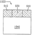
도 10E-10F의 평면 하이브리드 배향 반도체 기판 구조물(1020 및 1030)은 반도체 기판(930)이 절연 기판(1040)과 대체되어 있다는 점을 제외하고는 도 10A-10B의 구조물(1000 및 940)과 동일하다.
도 10G-10H의 평면 하이브리드 배향 반도체 기판 구조물(1050 및 1060)은 도 10C의 구조물(960)과 유사하지만, 트렌치 격리 영역(950)을 갖는다. 도 10G의 구조물(1050)에서, 트렌치 격리 영역(950)은 제1 단결정 반도체 영역(910)과 잔여물(990) 간의 인터페이스(1070) 아래로 연장되지만, BOX 층(970)에 이르지는 않는다. 도 10H의 구조물(1060)에서, 트렌치 격리 영역(950)은 BOX 층(970)으로 연장된다.
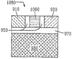
도 10I의 평면 하이브리드 배향 반도체 기판 구조물(1080)은 BOX 층(970)으로 연장된 트렌치 격리 영역(950)에 의해 분리된 세 개의 배향이 다른 단결정 반도 체 영역(910, 920 및 1090)을 포함한다. 세 개 이상의 표면 배향을 갖는 평면 하이브리드 배향 반도체 기판 구조물은 이중층 템플레이트 적층 대신에 다중층 템플레이트 적층을 이용하여 본 발명의 국부적 무결정 및 재결정 방법에 의해 형성될 수 있다.
도 5A-5B 및 도 10A-10I의 것과 유사한 구조물은 부가의 단계로 또는 부가의 단계 없이 기본 단계를 다양하게 치환하여 형성될 수 있다. 예를 들어, 도 5B의 평면 하이브리드 배향 구조물 유사물(460)이 제2 반도체 재료(920)의 잔여물(990)을 무결정화하고 단결정 영역(910)을 템플레이트으로 이용하여 무결정 영역을 재결정화하는 부가의 단계에 의해 도 10H의 구조물로부터 형성될 수 있다.
본 발명의 반도체 기판 및 단결정 반도체 영역은 폭 넓은 범위의 반도체 재료 중에서 선택될 수 있다. 예를 들어, 기판(510, 520, 700, 930 및 980) 및 다르게 배향된 제1 및 제2 반도체 영역(470, 610', 910 및 480, 650 및 920)은 Si, SiC, SiGe, SiGeC, Ge 합금, Ge, C, GaAs, InAs, InP 뿐만 아니라, 그 외 III-V 또는 II-VI 화합물 반도체 중에서 선택될 수 있다. 하나 이상의 도펀트를 갖거나 갖지 않는 상술한 반도체 재료 (예를 들어, SiGe 상의 Si 층)의 계층 조합이나 합금을 여기에서 생각할 수 있다. 제1 및 제2 반도체 영역은 변형되거나 비변형될 수 도 있고, 또는 변형층과 비변형층의 조합을 이용할 수도 있다. 결정 배향은 통상 (110), (111) 및 (100)을 포함하는 그룹에서 선택될 수 있다.
제1 및 제2 단결정 반도체 영역(470, 610', 910, 및 480, 650 및 920)의 두께는 통상 약 1 내지 약 500nm이고, 약 10 내지 약 100nm의 두께가 더욱 일반적이 다. 기판(510, 520, 700, 930 및 980)의 두께는 통상 5와 1000㎛ 사이이고, 가장 통상적으로는 약 600㎛이다.
BOX 층과 절연 기판(1040)은 이에만 제한되는 것은 아니지만 SiO2, 결정 SiO2, 질소나 그 외 원소를 함유하는 SiO2, 실리콘 질화물, 금속 산화물 (예를 들어, Al2O3), 절연 금속 질화물 (예를 들어, AlN), 결정 다이아몬드와 같은 고 열전도성을 포함하는 폭넓은 범위의 유전 재료 중에서 선택될 수 있다. BOX 두께는 약 2nm 내지 약 500nm의 범위이며, 통상 약 50 내지 약 150nm의 범위에 있는 것이 바람직하다.
템플레이트 적층을 형성하기 위한 본딩 방법은 당업자에게는 잘 알려진 방법을 포함한다 (예를 들어, Q.Y.Tong 등의 [in Semiconductor Wafer Bonding: Science and Technology (John Wiley, 1998)] 및 2003년 10월 29일자 출원된 함께 계류중이며 양도된 미국 특허 일련 번호 10/696,634 및 2003년 6월 17일자 출원된 함께 계류중이며 양도된 미국 특허 일련 번호 10/250,241 참조). 상기 기술된 함께 양도된 미국 출원 각각의 내용은 여기 참조로 언급되고 있다.
본딩되는 다르게 배향된 반도체 표면은 가장 깨끗한 인터페이스를 위해서 소수성 (친수성 보다는)인 것이 바람직한데, 이는 무결정 영역의 불순물이 통상 재결정화의 진행을 저해하기 때문이다. 그러나, 산화물이 적당한 어닐링으로 불연속적인 아일랜드 형태를 갖게 만들어질 수 있다면 본딩된 인터페이스에서의 매우 얇은 산화물은 허용 가능하다 (예를 들어, 2001년 9월 2 -7일, 샌프랜시스코, 반도체 웨 이퍼 본딩에 대한 6차 국제 심포지움에서 P.McCann 등의 "직접 실리콘 본딩시의 계면 산화물 조사" 참조). 본딩 이후의 웨이퍼 분리/제거는 웨이퍼를 연마하거나 에칭 (바람직하게는 에칭 정지층을 이용)하거나, 이전의 처리 단계에서 형성된 기계적으로 약한 인터페이스층을 이용하여 달성될 수 있다. 기계적으로 약한 인터페이스층의 예들은 다공성 Si (예를 들어, 2000년 6월, 고체 상태 기술에서 K.Sakaguchi 등에 의해 기술된 에피텍셜층 전이 (ELTRAN) 참조] 및 이온 주입 H 함유 버블 (예를 들어, 1994년 12월 20일 발해진 M.Bruel의 미국 특허 번호 5,374,564 및 1999년 3월 16일자 발해진 K.V.Strikrishnan의 미국 특허 번호 5,882,987에 기재된 스마트 커트 프로세스 (smart cut process) 참조).
무결정은 통상 이온 주입으로 실행된다. 최적의 이온 주입 조건은 템플레이트층의 재료, 템플레이트 층의 두께 및 무결정화된 적층 층의 위치 (상부 또는 하부)에 따라 다르다. 이들에만 제한되는 것은 아니지만, Si, Ge, Ar, C, O, N, H, He, Kr, Xe, P, B, As 등을 포함하는 당업자에게는 알려진 이온 종들이 이용될 수 있다. 무결정화를 위한 이온은 Si 또는 Ge인 것이 바람직하다. H와 He 등과 같은 더 가벼운 이온들은 통상 무결정화시 덜 효율적이다. 이온 주입은 극저온에서 공칭의 실온 이상의 몇백 ℃ 까지의 범위의 온도에서 실행될 수 있다. "공칭의 실온"이라는 것은 약 20℃에서 약 40℃의 온도를 의미한다. 무결정화되지 않은 영역은 통상 패턴화 마스크 (예를 들어, 실온 주입 프로세스 동안 패턴화된 포토레지스트)에 의해 이온 주입으로부터 보호될 수 있다. 주입은 "스크린 산화물" 층 있이 또는 없이 실행될 수 있으며 충분히 균일하게 무결정화된 영역이 단일 주입으로 쉽 게 성취될 수 없다면 다른 에너지에서 복수의 주입이 실행될 수 있다. 필요한 주입량은 주입 종, 주입되고 있는 반도체, 및 무결정화가 필요한 층의 두께에 따라 다르다. 총 6E15/㎠의 도스양으로 50, 100, 150 및 200keV에서 극저온 주입된 Si는 100 배향 및 110 배향된 Si의 상부 400nm를 무결정화하는 데에 충분한 것으로 밝혀졌다 (예를 들어, L.Csepregi 등 참조). 그러나, 더 낮은 도스량 (예를 들어, 40keV에서 5E14/㎠)은 주입된 이온이 Ge이고 무결정화된 표면 영역이 50-100nm 보다 더 얇을 때 Si를 무결정화할 수 있다.
국부적 무결정 영역(630, 730, 및 850)의 재결정화는 통상 원하는 재결정화를 초래하기 충분한 시간 동안, 약 200℃ 내지 약 1300℃의 온도에서, 바람직하게는 약 400℃에서 약 900℃에서, 더 바람직하게는 약 400℃ 내지 600℃에서 어닐링하여 행해진다. 이 주기는 템플레이트 층의 배향, 재결정화될 무결정 영역의 두께, 무결정층의 주입 및 그 외 불순물의 존재, 및 가능하다면 주입과 비주입 영역 간의 인터페이스의 예리함에 따라 달라지게 된다. 어닐링은 퍼니스 (furnace)에서 또는 급속 열 어닐링에 의해 실행된다. 다른 실시예에서, 어닐링은 레이저 어닐링이나 스파이크어닐링을 이용하여 실행될 수 있다. 어닐링 분위기는 통상 N2, Ar, He, H2 및 이들 가스의 혼합물을 포함하는 가스의 그룹 중에서 선택된다.
재결정화 단계에 이어 구조물에 매립 절연물이 형성될 때, 매립 절연층의 형성시 이용될 수 있는 종래의 이온 주입 단계와 어닐링 단계가 이용될 수 있다. 예를 들어, 종래의 SIMOX 프로세스는 도 8F-8G에 나타낸 구조물의 매립 산화물층을 제조할 때 이용될 수 있다.
본 발명의 몇 실시예는 그 변형예와 함께 여기에서 상세히 기재되었으며 첨부한 도면에서 도시되고 있으며, 여러 다른 변형이 본 발명의 영역에서 벗어나지 않고 가능하다는 것이 명백하다. 특히, 본 발명의 기판 구조물, 회로, 및 방법의 대부분은 두 다른 배향을 갖는 소수의 단결정 영역의 경우에 대해 설명되었지만, 본 발명은 이런 단결정 영역의 대부분을 제공하기 위한 방법과 이를 포함하는 구조물에도 동일하게 적용된다. 더욱, 본 발명의 하이브리드 배향 기판은 부가의 덧층 (에피텍셜 성장된 반도체나 부가의 본딩층), 특정 표면 특성의 제거나 에칭백 (예를 들어, 단결정 반도체 영역이나 트렌치 격리 중 하나 이상의 리세싱) 및/또는 특수한 도핑 프로파일과 결합될 수 있는데, 후속 제조된 소자에 대해 이런 기판 특성이 필요한 경우이다. 상기 설명은 본 발명을 다음 청구범위 보다 더욱 좁게 제한하고자 하는 것은 아니다. 이들 예들은 배타적이기보다는 설명적으로만 이해되어야 한다.
Claims (55)
- 평면 하이브리드 배향 기판을 형성하는 방법에 있어서:제1 배향을 갖는 제1 하부 단결정 반도체층, 제1 배향과 다른 제2 배향을 갖는 제2 상부 단결정 반도체층을 바닥부터 정상까지 포함하는 이중층 템플레이트 적층을 형성하는 단계;상기 이중층 템플레이트 적층의 일부를 하나 이상의 선택 영역에서 상기 제2 상부 단결정 반도체층의 정상 표면의 일부를 통해 이온 주입하는 것으로 무결정화하여 매장된 국부적 무결정 영역을 형성하는 단계, -여기서, 상기 매장된 국부적 무결정 영역은 제1 국부적 무결정 영역 및 제2 국부적 무결정 영역을 포함하고, 상기 제1 국부적 무결정 영역은 상기 제1 하부 단결정 반도체층의 비-무결정 부위의 정상 표면이 상기 제2 상부 단결정 반도체층의 비-무결정 부위의 바닥 표면과 접촉하는 계면의 평면 위에 위치되고, 상기 제2 국부적 무결정 영역은 상기 계면의 상기 평면 아래에 위치되고, 여기서 상기 매장된 국부적 무결정 영역은 상기 제2 상부 단결정층의 상기 비-무결정 부위의 노출된 정상 표면으로부터 수직적으로 분리된다.-; 및상기 이중층 템플레이트 적층의 상기 제2 상부 단결정 반도체층의 비-무결정 부위를 템플레이트로 이용하여 상기 매장된 국부적 무결정 영역을 재결정화하는 단계;를 포함하고, 이로 인해 상기 매장된 국부적 무결정 영역이 상기 제2 결정 배향을 갖는 재결정화된 단결정 반도체 부위로 변경되고, 여기서, 상기 계면의 상기 평면 위의 상기 이중층 템플레이트층의 전체는 상기 재결정 후에 상기 제2 배향을 갖고, 상기 계면의 상기 평면 아래의 상기 이중층 템플레이트층의 일부는 상기 제1 하부 단결정 반도체층의 상기 비-무결정 부위와 상기 재결정 후에 상기 제2 결정 배향을 갖는 상기 재결정화된 단결정 반도체 부위의 일부를 포함하는 평면 하이브리드 배향 기판을 형성하는 방법.
- 제1항에 있어서,상기 제1 하부 단결정 반도체층은 SOI 기판의 절연층상에 배치되는 평면 하이브리드 배향 기판을 형성하는 방법.
- 제1항에 있어서,상기 제1 하부 단결정 반도체층은 단결정 반도체 기판을 포함하는 평면 하이브리드 배향 기판을 형성하는 방법.
- 제1항에 있어서,상기 이중층 템플레이트 적층은 상기 제2 상부 단결정 반도체층을 상기 제1 하부 단결정 반도체층과 본딩하는 것으로 형성되고, 여기서 상기 제2 상부 단결정 반도체층은 상기 제1 하부 단결정 반도체층의 최정상부에 직접적으로 위치되는 평면 하이브리드 배향 기판을 형성하는 방법.
- 제1항에 있어서,상기 국부적 무결정 영역은 제1 하부 단결정 반도체층 내에 우세하게 형성되는 평면 하이브리드 배향 기판을 형성하는 방법.
- 제1항에 있어서,상기 하나 이상의 선택된 영역을 무결정화를 위해 선택되지 않은 적어도 다른 영역으로부터 분리하기 위해 하나 이상의 트랜치 격리 영역을 형성하는 단계를 더 포함하고, 여기서 상기 하나 이상의 트랜치 격리는 무결정화 전에, 무결정화 및 재결정화 사이에 또는 부분적으로 무결정화 후 및 부분적으로 재결정화 후에 형성되는 것인 평면 하이브리드 배향 기판을 형성하는 방법.
- 제1항에 있어서,상기 제1 하부 단결정 반도체층 및 상기 제2 상부 단결정 반도체층은 Si, SiC, SiGe, SiGeC, Ge 합금, Ge, C, GaAs, InAs, InP, 계층 조합 또는 이들의 합금 및 다른 III-VI 또는 II-VI 화합물 반도체로 이루어진 군에서 선택된 동일하거나 다른 반도체 물질로 구성되는 평면 하이브리드 배향 기판을 형성하는 방법.
- 제1항에 있어서,상기 제1 하부 단결정 반도체층 및 상기 제2 상부 단결정 반도체층은 모두 Si-함유 반도체 물질로 구성되는 것인 평면 하이브리드 배향 기판을 형성하는 방법.
- 제1항에 있어서,상기 제1 하부 단결정 반도체층과 상기 제2 상부 단결정 반도체층은 변형된 반도체 물질, 비변형된 반도체 물질 또는 변형 및 비변형된 반도체 물질의 조합물로 구성되는 평면 하이브리드 배향 기판을 형성하는 방법.
- 제1항에 있어서,상기 제1 하부 단결정 반도체층과 상기 제2 상부 단결정 반도체층은 (110), (111) 및 (100)으로부터 선택된 다른 표면 배향을 갖는 평면 하이브리드 배향 기판을 형성하는 방법.
- 삭제
- 삭제
- 삭제
- 삭제
- 삭제
- 삭제
- 삭제
- 삭제
- 삭제
- 삭제
- 삭제
- 삭제
- 삭제
- 삭제
- 삭제
- 삭제
- 삭제
- 삭제
- 삭제
- 삭제
- 삭제
- 삭제
- 삭제
- 삭제
- 삭제
- 삭제
- 삭제
- 삭제
- 삭제
- 삭제
- 삭제
- 삭제
- 삭제
- 삭제
- 삭제
- 삭제
- 삭제
- 삭제
- 삭제
- 삭제
- 삭제
- 삭제
- 삭제
- 삭제
- 삭제
Applications Claiming Priority (2)
| Application Number | Priority Date | Filing Date | Title |
|---|---|---|---|
| US10/725,850 | 2003-12-02 | ||
| US10/725,850 US20050116290A1 (en) | 2003-12-02 | 2003-12-02 | Planar substrate with selected semiconductor crystal orientations formed by localized amorphization and recrystallization of stacked template layers |
Publications (2)
| Publication Number | Publication Date |
|---|---|
| KR20060130572A KR20060130572A (ko) | 2006-12-19 |
| KR100961800B1 true KR100961800B1 (ko) | 2010-06-08 |
Family
ID=34620372
Family Applications (1)
| Application Number | Title | Priority Date | Filing Date |
|---|---|---|---|
| KR1020067010604A KR100961800B1 (ko) | 2003-12-02 | 2004-11-30 | 적층형 템플레이트 층의 국부적 무결정 및 재결정으로형성된 선택적 반도체 결정 배향을 갖는 평면 기판 |
Country Status (7)
| Country | Link |
|---|---|
| US (2) | US20050116290A1 (ko) |
| EP (1) | EP1702350A2 (ko) |
| JP (1) | JP5063114B2 (ko) |
| KR (1) | KR100961800B1 (ko) |
| CN (1) | CN100505273C (ko) |
| TW (1) | TWI328286B (ko) |
| WO (1) | WO2005057631A2 (ko) |
Families Citing this family (124)
| Publication number | Priority date | Publication date | Assignee | Title |
|---|---|---|---|---|
| JP2004119943A (ja) * | 2002-09-30 | 2004-04-15 | Renesas Technology Corp | 半導体ウェハおよびその製造方法 |
| US20050116290A1 (en) | 2003-12-02 | 2005-06-02 | De Souza Joel P. | Planar substrate with selected semiconductor crystal orientations formed by localized amorphization and recrystallization of stacked template layers |
| US7291886B2 (en) * | 2004-06-21 | 2007-11-06 | International Business Machines Corporation | Hybrid substrate technology for high-mobility planar and multiple-gate MOSFETs |
| US7253034B2 (en) * | 2004-07-29 | 2007-08-07 | International Business Machines Corporation | Dual SIMOX hybrid orientation technology (HOT) substrates |
| US7354806B2 (en) * | 2004-09-17 | 2008-04-08 | International Business Machines Corporation | Semiconductor device structure with active regions having different surface directions and methods |
| US7235433B2 (en) | 2004-11-01 | 2007-06-26 | Advanced Micro Devices, Inc. | Silicon-on-insulator semiconductor device with silicon layers having different crystal orientations and method of forming the silicon-on-insulator semiconductor device |
| DE102004057764B4 (de) * | 2004-11-30 | 2013-05-16 | Advanced Micro Devices, Inc. | Verfahren zur Herstellung eines Substrats mit kristallinen Halbleitergebieten mit unterschiedlichen Eigenschaften, die über einem kristallinen Vollsubstrat angeordnet sind und damit hergestelltes Halbleiterbauelement |
| US7393733B2 (en) * | 2004-12-01 | 2008-07-01 | Amberwave Systems Corporation | Methods of forming hybrid fin field-effect transistor structures |
| US7422956B2 (en) * | 2004-12-08 | 2008-09-09 | Advanced Micro Devices, Inc. | Semiconductor device and method of making semiconductor device comprising multiple stacked hybrid orientation layers |
| US7285473B2 (en) * | 2005-01-07 | 2007-10-23 | International Business Machines Corporation | Method for fabricating low-defect-density changed orientation Si |
| US8138061B2 (en) * | 2005-01-07 | 2012-03-20 | International Business Machines Corporation | Quasi-hydrophobic Si-Si wafer bonding using hydrophilic Si surfaces and dissolution of interfacial bonding oxide |
| US20060175659A1 (en) * | 2005-02-07 | 2006-08-10 | International Business Machines Corporation | A cmos structure for body ties in ultra-thin soi (utsoi) substrates |
| US7547917B2 (en) * | 2005-04-06 | 2009-06-16 | International Business Machines Corporation | Inverted multilayer semiconductor device assembly |
| US7250351B2 (en) * | 2005-04-14 | 2007-07-31 | International Business Machines Corporation | Enhanced silicon-on-insulator (SOI) transistors and methods of making enhanced SOI transistors |
| US7291539B2 (en) * | 2005-06-01 | 2007-11-06 | International Business Machines Corporation | Amorphization/templated recrystallization method for hybrid orientation substrates |
| US7358164B2 (en) * | 2005-06-16 | 2008-04-15 | International Business Machines Corporation | Crystal imprinting methods for fabricating substrates with thin active silicon layers |
| US7473985B2 (en) * | 2005-06-16 | 2009-01-06 | International Business Machines Corporation | Hybrid oriented substrates and crystal imprinting methods for forming such hybrid oriented substrates |
| US7439108B2 (en) * | 2005-06-16 | 2008-10-21 | International Business Machines Corporation | Coplanar silicon-on-insulator (SOI) regions of different crystal orientations and methods of making the same |
| US7344962B2 (en) * | 2005-06-21 | 2008-03-18 | International Business Machines Corporation | Method of manufacturing dual orientation wafers |
| US7217629B2 (en) * | 2005-07-15 | 2007-05-15 | International Business Machines Corporation | Epitaxial imprinting |
| US20070040235A1 (en) * | 2005-08-19 | 2007-02-22 | International Business Machines Corporation | Dual trench isolation for CMOS with hybrid orientations |
| DE102005052055B3 (de) * | 2005-10-31 | 2007-04-26 | Advanced Micro Devices, Inc., Sunnyvale | Eingebettete Verformungsschicht in dünnen SOI-Transistoren und Verfahren zur Herstellung desselben |
| WO2007053382A1 (en) * | 2005-10-31 | 2007-05-10 | Advanced Micro Devices, Inc. | An embedded strain layer in thin soi transistors and a method of forming the same |
| US7535089B2 (en) * | 2005-11-01 | 2009-05-19 | Massachusetts Institute Of Technology | Monolithically integrated light emitting devices |
| US7986029B2 (en) * | 2005-11-08 | 2011-07-26 | Taiwan Semiconductor Manufacturing Company, Ltd. | Dual SOI structure |
| US7288458B2 (en) * | 2005-12-14 | 2007-10-30 | Freescale Semiconductor, Inc. | SOI active layer with different surface orientation |
| US7569466B2 (en) * | 2005-12-16 | 2009-08-04 | International Business Machines Corporation | Dual metal gate self-aligned integration |
| US7436034B2 (en) * | 2005-12-19 | 2008-10-14 | International Business Machines Corporation | Metal oxynitride as a pFET material |
| US8319285B2 (en) * | 2005-12-22 | 2012-11-27 | Infineon Technologies Ag | Silicon-on-insulator chip having multiple crystal orientations |
| US8530355B2 (en) * | 2005-12-23 | 2013-09-10 | Infineon Technologies Ag | Mixed orientation semiconductor device and method |
| US7432567B2 (en) * | 2005-12-28 | 2008-10-07 | International Business Machines Corporation | Metal gate CMOS with at least a single gate metal and dual gate dielectrics |
| US7833849B2 (en) | 2005-12-30 | 2010-11-16 | International Business Machines Corporation | Method of fabricating a semiconductor structure including one device region having a metal gate electrode located atop a thinned polygate electrode |
| US7425497B2 (en) | 2006-01-20 | 2008-09-16 | International Business Machines Corporation | Introduction of metal impurity to change workfunction of conductive electrodes |
| US7285452B2 (en) * | 2006-02-10 | 2007-10-23 | Sadaka Mariam G | Method to selectively form regions having differing properties and structure |
| US7531392B2 (en) * | 2006-02-27 | 2009-05-12 | International Business Machines Corporation | Multi-orientation semiconductor-on-insulator (SOI) substrate, and method of fabricating same |
| US20070215984A1 (en) * | 2006-03-15 | 2007-09-20 | Shaheen Mohamad A | Formation of a multiple crystal orientation substrate |
| US7396407B2 (en) * | 2006-04-18 | 2008-07-08 | International Business Machines Corporation | Trench-edge-defect-free recrystallization by edge-angle-optimized solid phase epitaxy: method and applications to hybrid orientation substrates |
| US7521307B2 (en) * | 2006-04-28 | 2009-04-21 | International Business Machines Corporation | CMOS structures and methods using self-aligned dual stressed layers |
| US7452784B2 (en) | 2006-05-25 | 2008-11-18 | International Business Machines Corporation | Formation of improved SOI substrates using bulk semiconductor wafers |
| US7435639B2 (en) * | 2006-05-31 | 2008-10-14 | Freescale Semiconductor, Inc. | Dual surface SOI by lateral epitaxial overgrowth |
| US20080048269A1 (en) * | 2006-08-25 | 2008-02-28 | International Business Machines Corporation | Method of fabricating structure for integrated circuit incorporating hybrid orientation technology and trench isolation regions |
| US7595232B2 (en) | 2006-09-07 | 2009-09-29 | International Business Machines Corporation | CMOS devices incorporating hybrid orientation technology (HOT) with embedded connectors |
| US7820501B2 (en) * | 2006-10-11 | 2010-10-26 | International Business Machines Corporation | Decoder for a stationary switch machine |
| US20080128821A1 (en) * | 2006-12-04 | 2008-06-05 | Texas Instruments Incorporated | Semiconductor Device Manufactured Using Passivation of Crystal Domain Interfaces in Hybrid Orientation Technology |
| US20080164572A1 (en) * | 2006-12-21 | 2008-07-10 | Covalent Materials Corporation | Semiconductor substrate and manufacturing method thereof |
| JP2008177529A (ja) * | 2006-12-21 | 2008-07-31 | Covalent Materials Corp | 半導体基板およびその製造方法 |
| US20080169535A1 (en) * | 2007-01-12 | 2008-07-17 | International Business Machines Corporation | Sub-lithographic faceting for mosfet performance enhancement |
| US8016941B2 (en) * | 2007-02-05 | 2011-09-13 | Infineon Technologies Ag | Method and apparatus for manufacturing a semiconductor |
| US7611979B2 (en) * | 2007-02-12 | 2009-11-03 | International Business Machines Corporation | Metal gates with low charge trapping and enhanced dielectric reliability characteristics for high-k gate dielectric stacks |
| US7608522B2 (en) * | 2007-03-11 | 2009-10-27 | United Microelectronics Corp. | Method for fabricating a hybrid orientation substrate |
| US9034102B2 (en) * | 2007-03-29 | 2015-05-19 | United Microelectronics Corp. | Method of fabricating hybrid orientation substrate and structure of the same |
| US20080248626A1 (en) * | 2007-04-05 | 2008-10-09 | International Business Machines Corporation | Shallow trench isolation self-aligned to templated recrystallization boundary |
| US7651902B2 (en) * | 2007-04-20 | 2010-01-26 | International Business Machines Corporation | Hybrid substrates and methods for forming such hybrid substrates |
| FR2915318B1 (fr) * | 2007-04-20 | 2009-07-17 | St Microelectronics Crolles 2 | Procede de realisation d'un circuit electronique integre a deux portions de couches actives ayant des orientations cristallines differentes |
| US7750406B2 (en) * | 2007-04-20 | 2010-07-06 | International Business Machines Corporation | Design structure incorporating a hybrid substrate |
| US7575968B2 (en) * | 2007-04-30 | 2009-08-18 | Freescale Semiconductor, Inc. | Inverse slope isolation and dual surface orientation integration |
| US7547641B2 (en) * | 2007-06-05 | 2009-06-16 | International Business Machines Corporation | Super hybrid SOI CMOS devices |
| FR2917235B1 (fr) * | 2007-06-06 | 2010-09-03 | Soitec Silicon On Insulator | Procede de realisation de composants hybrides. |
| FR2913815A1 (fr) * | 2007-06-06 | 2008-09-19 | Soitec Silicon On Insulator | PROCEDE DE CO-INTEGRATION DE SEMI-CONDUCTEURS, EN PARTICULIER SOI ET GeOI OU GaAsOI |
| US7989306B2 (en) * | 2007-06-29 | 2011-08-02 | International Business Machines Corporation | Method of forming alternating regions of Si and SiGe or SiGeC on a buried oxide layer on a substrate |
| US20090008725A1 (en) * | 2007-07-03 | 2009-01-08 | International Business Machines Corporation | Method for deposition of an ultra-thin electropositive metal-containing cap layer |
| FR2918793B1 (fr) * | 2007-07-11 | 2009-10-09 | Commissariat Energie Atomique | Procede de fabrication d'un substrat semiconducteur-sur- isolant pour la microelectronique et l'optoelectronique. |
| US8803195B2 (en) * | 2007-08-02 | 2014-08-12 | Wisconsin Alumni Research Foundation | Nanomembrane structures having mixed crystalline orientations and compositions |
| US7808020B2 (en) * | 2007-10-09 | 2010-10-05 | International Business Machines Corporation | Self-assembled sidewall spacer |
| US8105960B2 (en) * | 2007-10-09 | 2012-01-31 | International Business Machines Corporation | Self-assembled sidewall spacer |
| US7863712B2 (en) * | 2007-10-30 | 2011-01-04 | International Business Machines Corporation | Hybrid orientation semiconductor structure with reduced boundary defects and method of forming same |
| US7696573B2 (en) * | 2007-10-31 | 2010-04-13 | International Business Machines Corporation | Multiple crystallographic orientation semiconductor structures |
| US8043947B2 (en) * | 2007-11-16 | 2011-10-25 | Texas Instruments Incorporated | Method to eliminate re-crystallization border defects generated during solid phase epitaxy of a DSB substrate |
| US8288756B2 (en) * | 2007-11-30 | 2012-10-16 | Advanced Micro Devices, Inc. | Hetero-structured, inverted-T field effect transistor |
| WO2009095813A1 (en) * | 2008-01-28 | 2009-08-06 | Nxp B.V. | A method for fabricating a dual-orientation group-iv semiconductor substrate |
| WO2009128776A1 (en) * | 2008-04-15 | 2009-10-22 | Vallin Oerjan | Hybrid wafers with hybrid-oriented layer |
| US8241970B2 (en) | 2008-08-25 | 2012-08-14 | International Business Machines Corporation | CMOS with channel P-FinFET and channel N-FinFET having different crystalline orientations and parallel fins |
| JP2010072209A (ja) * | 2008-09-17 | 2010-04-02 | Fuji Xerox Co Ltd | 静電荷像現像用トナー、静電荷像現像用トナーの製造方法、静電荷像現像用現像剤および画像形成装置 |
| FR2938117B1 (fr) * | 2008-10-31 | 2011-04-15 | Commissariat Energie Atomique | Procede d'elaboration d'un substrat hybride ayant une couche continue electriquement isolante enterree |
| FR2942674B1 (fr) * | 2009-02-27 | 2011-12-16 | Commissariat Energie Atomique | Procede d'elaboration d'un substrat hybride par recristallisation partielle d'une couche mixte |
| US8227307B2 (en) * | 2009-06-24 | 2012-07-24 | International Business Machines Corporation | Method for removing threshold voltage adjusting layer with external acid diffusion process |
| US8105892B2 (en) * | 2009-08-18 | 2012-01-31 | International Business Machines Corporation | Thermal dual gate oxide device integration |
| US8022488B2 (en) | 2009-09-24 | 2011-09-20 | International Business Machines Corporation | High-performance FETs with embedded stressors |
| US7943458B2 (en) * | 2009-10-06 | 2011-05-17 | International Business Machines Corporation | Methods for obtaining gate stacks with tunable threshold voltage and scaling |
| US8288222B2 (en) | 2009-10-20 | 2012-10-16 | International Business Machines Corporation | Application of cluster beam implantation for fabricating threshold voltage adjusted FETs |
| US8035141B2 (en) | 2009-10-28 | 2011-10-11 | International Business Machines Corporation | Bi-layer nFET embedded stressor element and integration to enhance drive current |
| FR2954584B1 (fr) * | 2009-12-22 | 2013-07-19 | Commissariat Energie Atomique | Substrat hybride a isolation amelioree et procede de realisation simplifie d'un substrat hybride |
| US8445974B2 (en) | 2010-01-07 | 2013-05-21 | International Business Machines Corporation | Asymmetric FET including sloped threshold voltage adjusting material layer and method of fabricating same |
| US8299530B2 (en) | 2010-03-04 | 2012-10-30 | International Business Machines Corporation | Structure and method to fabricate pFETS with superior GIDL by localizing workfunction |
| US8450807B2 (en) | 2010-03-09 | 2013-05-28 | International Business Machines Corporation | MOSFETs with reduced contact resistance |
| KR101642834B1 (ko) | 2010-04-09 | 2016-08-11 | 삼성전자주식회사 | Leg 공정을 이용하여 벌크 실리콘 웨이퍼의 필요한 영역내에 soⅰ층을 형성하는 반도체 소자의 제조방법 |
| US8236660B2 (en) | 2010-04-21 | 2012-08-07 | International Business Machines Corporation | Monolayer dopant embedded stressor for advanced CMOS |
| US8299535B2 (en) | 2010-06-25 | 2012-10-30 | International Business Machines Corporation | Delta monolayer dopants epitaxy for embedded source/drain silicide |
| US8361889B2 (en) | 2010-07-06 | 2013-01-29 | International Business Machines Corporation | Strained semiconductor-on-insulator by addition and removal of atoms in a semiconductor-on-insulator |
| US8962417B2 (en) | 2010-10-15 | 2015-02-24 | International Business Machines Corporation | Method and structure for pFET junction profile with SiGe channel |
| US8659054B2 (en) | 2010-10-15 | 2014-02-25 | International Business Machines Corporation | Method and structure for pFET junction profile with SiGe channel |
| US8466473B2 (en) | 2010-12-06 | 2013-06-18 | International Business Machines Corporation | Structure and method for Vt tuning and short channel control with high k/metal gate MOSFETs |
| US8564063B2 (en) | 2010-12-07 | 2013-10-22 | United Microelectronics Corp. | Semiconductor device having metal gate and manufacturing method thereof |
| US8536656B2 (en) | 2011-01-10 | 2013-09-17 | International Business Machines Corporation | Self-aligned contacts for high k/metal gate process flow |
| US8643115B2 (en) | 2011-01-14 | 2014-02-04 | International Business Machines Corporation | Structure and method of Tinv scaling for high κ metal gate technology |
| CN102790084B (zh) * | 2011-05-16 | 2016-03-16 | 中国科学院上海微系统与信息技术研究所 | 锗和iii-v混合共平面的soi半导体结构及其制备方法 |
| US8432002B2 (en) * | 2011-06-28 | 2013-04-30 | International Business Machines Corporation | Method and structure for low resistive source and drain regions in a replacement metal gate process flow |
| US9064808B2 (en) * | 2011-07-25 | 2015-06-23 | Synopsys, Inc. | Integrated circuit devices having features with reduced edge curvature and methods for manufacturing the same |
| US8609550B2 (en) | 2011-09-08 | 2013-12-17 | Synopsys, Inc. | Methods for manufacturing integrated circuit devices having features with reduced edge curvature |
| FR2983342B1 (fr) * | 2011-11-30 | 2016-05-20 | Soitec Silicon On Insulator | Procede de fabrication d'une heterostructure limitant la formation de defauts et heterostructure ainsi obtenue |
| CN102768982A (zh) * | 2012-07-06 | 2012-11-07 | 上海新傲科技股份有限公司 | 带有绝缘埋层的混合晶向衬底的制备方法 |
| CN102768983A (zh) * | 2012-07-12 | 2012-11-07 | 上海新傲科技股份有限公司 | 带有绝缘埋层的混合晶向衬底的制备方法 |
| JP2014093319A (ja) * | 2012-10-31 | 2014-05-19 | Toshiba Corp | 半導体装置およびその製造方法 |
| CN103871813A (zh) * | 2012-12-14 | 2014-06-18 | 中国科学院微电子研究所 | 一种半导体离子注入均匀性的改善方法 |
| FR3003685B1 (fr) | 2013-03-21 | 2015-04-17 | St Microelectronics Crolles 2 | Procede de modification localisee des contraintes dans un substrat du type soi, en particulier fd soi, et dispositif correspondant |
| US9059095B2 (en) | 2013-04-22 | 2015-06-16 | International Business Machines Corporation | Self-aligned borderless contacts using a photo-patternable dielectric material as a replacement contact |
| US8999791B2 (en) | 2013-05-03 | 2015-04-07 | International Business Machines Corporation | Formation of semiconductor structures with variable gate lengths |
| US9214567B2 (en) | 2013-09-06 | 2015-12-15 | Globalfoundries Inc. | Nanowire compatible E-fuse |
| US8951868B1 (en) | 2013-11-05 | 2015-02-10 | International Business Machines Corporation | Formation of functional gate structures with different critical dimensions using a replacement gate process |
| CN103745952B (zh) * | 2013-12-25 | 2016-04-06 | 上海新傲科技股份有限公司 | 带有绝缘埋层的混晶衬底的制备方法 |
| US9595525B2 (en) | 2014-02-10 | 2017-03-14 | International Business Machines Corporation | Semiconductor device including nanowire transistors with hybrid channels |
| US9093425B1 (en) | 2014-02-11 | 2015-07-28 | International Business Machines Corporation | Self-aligned liner formed on metal semiconductor alloy contacts |
| US9184290B2 (en) | 2014-04-02 | 2015-11-10 | International Business Machines Corporation | Method of forming well-controlled extension profile in MOSFET by silicon germanium based sacrificial layer |
| US9293375B2 (en) | 2014-04-24 | 2016-03-22 | International Business Machines Corporation | Selectively grown self-aligned fins for deep isolation integration |
| US9490161B2 (en) | 2014-04-29 | 2016-11-08 | International Business Machines Corporation | Channel SiGe devices with multiple threshold voltages on hybrid oriented substrates, and methods of manufacturing same |
| US9331076B2 (en) | 2014-05-02 | 2016-05-03 | International Business Machines Corporation | Group III nitride integration with CMOS technology |
| US10056293B2 (en) * | 2014-07-18 | 2018-08-21 | International Business Machines Corporation | Techniques for creating a local interconnect using a SOI wafer |
| US9412840B1 (en) | 2015-05-06 | 2016-08-09 | International Business Machines Corporation | Sacrificial layer for replacement metal semiconductor alloy contact formation |
| US9666493B2 (en) | 2015-06-24 | 2017-05-30 | International Business Machines Corporation | Semiconductor device structure with 110-PFET and 111-NFET curent flow direction |
| FR3076292B1 (fr) * | 2017-12-28 | 2020-01-03 | Commissariat A L'energie Atomique Et Aux Energies Alternatives | Procede de transfert d'une couche utile sur un substrat support |
| US11139402B2 (en) | 2018-05-14 | 2021-10-05 | Synopsys, Inc. | Crystal orientation engineering to achieve consistent nanowire shapes |
| US11011411B2 (en) * | 2019-03-22 | 2021-05-18 | International Business Machines Corporation | Semiconductor wafer having integrated circuits with bottom local interconnects |
| US11264458B2 (en) | 2019-05-20 | 2022-03-01 | Synopsys, Inc. | Crystal orientation engineering to achieve consistent nanowire shapes |
| US11854816B2 (en) * | 2021-08-27 | 2023-12-26 | Taiwan Semiconductor Manufacturing Company, Ltd. | Semiconductor devices and methods of manufacturing thereof |
Family Cites Families (29)
| Publication number | Priority date | Publication date | Assignee | Title |
|---|---|---|---|---|
| US4385937A (en) * | 1980-05-20 | 1983-05-31 | Tokyo Shibaura Denki Kabushiki Kaisha | Regrowing selectively formed ion amorphosized regions by thermal gradient |
| JPS60154548A (ja) * | 1984-01-24 | 1985-08-14 | Fujitsu Ltd | 半導体装置の製造方法 |
| US4768076A (en) * | 1984-09-14 | 1988-08-30 | Hitachi, Ltd. | Recrystallized CMOS with different crystal planes |
| US4659392A (en) * | 1985-03-21 | 1987-04-21 | Hughes Aircraft Company | Selective area double epitaxial process for fabricating silicon-on-insulator structures for use with MOS devices and integrated circuits |
| DE3688318T2 (de) * | 1985-12-19 | 1993-07-29 | Sumitomo Electric Industries | Feldeffekttransistor. |
| US4775641A (en) * | 1986-09-25 | 1988-10-04 | General Electric Company | Method of making silicon-on-sapphire semiconductor devices |
| US4816893A (en) * | 1987-02-24 | 1989-03-28 | Hughes Aircraft Company | Low leakage CMOS/insulator substrate devices and method of forming the same |
| US4863877A (en) * | 1987-11-13 | 1989-09-05 | Kopin Corporation | Ion implantation and annealing of compound semiconductor layers |
| JPH01162362A (ja) * | 1987-12-18 | 1989-06-26 | Fujitsu Ltd | 半導体装置の製造方法 |
| JPH01162376A (ja) * | 1987-12-18 | 1989-06-26 | Fujitsu Ltd | 半導体装置の製造方法 |
| JPH03285351A (ja) * | 1990-04-02 | 1991-12-16 | Oki Electric Ind Co Ltd | Cmis型半導体装置およびその製造方法 |
| JPH04372166A (ja) * | 1991-06-21 | 1992-12-25 | Matsushita Electric Ind Co Ltd | 半導体装置の製造方法 |
| FR2681472B1 (fr) | 1991-09-18 | 1993-10-29 | Commissariat Energie Atomique | Procede de fabrication de films minces de materiau semiconducteur. |
| JP3017860B2 (ja) * | 1991-10-01 | 2000-03-13 | 株式会社東芝 | 半導体基体およびその製造方法とその半導体基体を用いた半導体装置 |
| JP3156878B2 (ja) * | 1992-04-30 | 2001-04-16 | 株式会社東芝 | 半導体装置およびその製造方法 |
| US5554562A (en) * | 1995-04-06 | 1996-09-10 | Advanced Micro Devices, Inc. | Advanced isolation scheme for deep submicron technology |
| US5888872A (en) * | 1997-06-20 | 1999-03-30 | Advanced Micro Devices, Inc. | Method for forming source drain junction areas self-aligned between a sidewall spacer and an etched lateral sidewall |
| US5882987A (en) | 1997-08-26 | 1999-03-16 | International Business Machines Corporation | Smart-cut process for the production of thin semiconductor material films |
| JP4521542B2 (ja) * | 1999-03-30 | 2010-08-11 | ルネサスエレクトロニクス株式会社 | 半導体装置および半導体基板 |
| EP1073112A1 (en) * | 1999-07-26 | 2001-01-31 | STMicroelectronics S.r.l. | Process for the manufacturing of a SOI wafer by oxidation of buried cavities |
| US6229187B1 (en) * | 1999-10-20 | 2001-05-08 | Advanced Micro Devices, Inc. | Field effect transistor with non-floating body and method for forming same on a bulk silicon wafer |
| US6407425B1 (en) * | 2000-09-21 | 2002-06-18 | Texas Instruments Incorporated | Programmable neuron MOSFET on SOI |
| US6782759B2 (en) * | 2001-07-09 | 2004-08-31 | Nartron Corporation | Anti-entrapment system |
| JP3782021B2 (ja) * | 2002-02-22 | 2006-06-07 | 株式会社東芝 | 半導体装置、半導体装置の製造方法、半導体基板の製造方法 |
| US6902962B2 (en) * | 2003-04-04 | 2005-06-07 | Taiwan Semiconductor Manufacturing Company, Ltd. | Silicon-on-insulator chip with multiple crystal orientations |
| US7329923B2 (en) | 2003-06-17 | 2008-02-12 | International Business Machines Corporation | High-performance CMOS devices on hybrid crystal oriented substrates |
| US6815278B1 (en) * | 2003-08-25 | 2004-11-09 | International Business Machines Corporation | Ultra-thin silicon-on-insulator and strained-silicon-direct-on-insulator with hybrid crystal orientations |
| US7023055B2 (en) | 2003-10-29 | 2006-04-04 | International Business Machines Corporation | CMOS on hybrid substrate with different crystal orientations using silicon-to-silicon direct wafer bonding |
| US20050116290A1 (en) | 2003-12-02 | 2005-06-02 | De Souza Joel P. | Planar substrate with selected semiconductor crystal orientations formed by localized amorphization and recrystallization of stacked template layers |
-
2003
- 2003-12-02 US US10/725,850 patent/US20050116290A1/en not_active Abandoned
-
2004
- 2004-11-09 CN CNB2004100923713A patent/CN100505273C/zh not_active Expired - Fee Related
- 2004-11-12 TW TW093134666A patent/TWI328286B/zh not_active IP Right Cessation
- 2004-11-30 KR KR1020067010604A patent/KR100961800B1/ko not_active IP Right Cessation
- 2004-11-30 EP EP04812491A patent/EP1702350A2/en not_active Withdrawn
- 2004-11-30 WO PCT/US2004/039970 patent/WO2005057631A2/en active Application Filing
- 2004-11-30 JP JP2006542666A patent/JP5063114B2/ja not_active Expired - Fee Related
-
2006
- 2006-12-04 US US11/566,579 patent/US7785939B2/en not_active Expired - Fee Related
Also Published As
| Publication number | Publication date |
|---|---|
| US7785939B2 (en) | 2010-08-31 |
| US20080108184A1 (en) | 2008-05-08 |
| WO2005057631A2 (en) | 2005-06-23 |
| TWI328286B (en) | 2010-08-01 |
| KR20060130572A (ko) | 2006-12-19 |
| WO2005057631A3 (en) | 2007-05-10 |
| CN100505273C (zh) | 2009-06-24 |
| JP5063114B2 (ja) | 2012-10-31 |
| CN1630087A (zh) | 2005-06-22 |
| US20050116290A1 (en) | 2005-06-02 |
| EP1702350A2 (en) | 2006-09-20 |
| TW200529423A (en) | 2005-09-01 |
| JP2007535802A (ja) | 2007-12-06 |
Similar Documents
| Publication | Publication Date | Title |
|---|---|---|
| KR100961800B1 (ko) | 적층형 템플레이트 층의 국부적 무결정 및 재결정으로형성된 선택적 반도체 결정 배향을 갖는 평면 기판 | |
| US7060585B1 (en) | Hybrid orientation substrates by in-place bonding and amorphization/templated recrystallization | |
| US7402466B2 (en) | Strained silicon CMOS on hybrid crystal orientations | |
| US7023057B2 (en) | CMOS on hybrid substrate with different crystal orientations using silicon-to-silicon direct wafer bonding | |
| US7393732B2 (en) | Double silicon-on-insulator (SOI) metal oxide semiconductor field effect transistor (MOSFET) structures | |
| US7468538B2 (en) | Strained silicon on a SiGe on SOI substrate | |
| US9355887B2 (en) | Dual trench isolation for CMOS with hybrid orientations | |
| US7253034B2 (en) | Dual SIMOX hybrid orientation technology (HOT) substrates | |
| JP2007535802A5 (ko) | ||
| US20130082350A1 (en) | Silicon-on-insulator chip having multiple crystal orientations | |
| US7217629B2 (en) | Epitaxial imprinting | |
| US7531392B2 (en) | Multi-orientation semiconductor-on-insulator (SOI) substrate, and method of fabricating same | |
| US7579254B2 (en) | Process for realizing an integrated electronic circuit with two active layer portions having different crystal orientations | |
| JP2004128254A (ja) | 半導体装置 | |
| JP2004296744A (ja) | 半導体装置の製造方法 | |
| JP2007109690A (ja) | 半導体装置およびその製造方法 |
Legal Events
| Date | Code | Title | Description |
|---|---|---|---|
| A201 | Request for examination | ||
| E902 | Notification of reason for refusal | ||
| E701 | Decision to grant or registration of patent right | ||
| GRNT | Written decision to grant | ||
| LAPS | Lapse due to unpaid annual fee |