JP4955935B2 - 貫通孔形成方法および半導体装置の製造方法 - Google Patents
貫通孔形成方法および半導体装置の製造方法 Download PDFInfo
- Publication number
- JP4955935B2 JP4955935B2 JP2005141086A JP2005141086A JP4955935B2 JP 4955935 B2 JP4955935 B2 JP 4955935B2 JP 2005141086 A JP2005141086 A JP 2005141086A JP 2005141086 A JP2005141086 A JP 2005141086A JP 4955935 B2 JP4955935 B2 JP 4955935B2
- Authority
- JP
- Japan
- Prior art keywords
- hole
- silicon substrate
- crystal plane
- etching
- opening
- Prior art date
- Legal status (The legal status is an assumption and is not a legal conclusion. Google has not performed a legal analysis and makes no representation as to the accuracy of the status listed.)
- Expired - Fee Related
Links
Images


Classifications
-
- H—ELECTRICITY
- H01—ELECTRIC ELEMENTS
- H01L—SEMICONDUCTOR DEVICES NOT COVERED BY CLASS H10
- H01L21/00—Processes or apparatus adapted for the manufacture or treatment of semiconductor or solid state devices or of parts thereof
- H01L21/70—Manufacture or treatment of devices consisting of a plurality of solid state components formed in or on a common substrate or of parts thereof; Manufacture of integrated circuit devices or of parts thereof
- H01L21/71—Manufacture of specific parts of devices defined in group H01L21/70
- H01L21/768—Applying interconnections to be used for carrying current between separate components within a device comprising conductors and dielectrics
- H01L21/76898—Applying interconnections to be used for carrying current between separate components within a device comprising conductors and dielectrics formed through a semiconductor substrate
-
- H—ELECTRICITY
- H01—ELECTRIC ELEMENTS
- H01L—SEMICONDUCTOR DEVICES NOT COVERED BY CLASS H10
- H01L23/00—Details of semiconductor or other solid state devices
- H01L23/48—Arrangements for conducting electric current to or from the solid state body in operation, e.g. leads, terminal arrangements ; Selection of materials therefor
- H01L23/481—Internal lead connections, e.g. via connections, feedthrough structures
-
- H—ELECTRICITY
- H01—ELECTRIC ELEMENTS
- H01L—SEMICONDUCTOR DEVICES NOT COVERED BY CLASS H10
- H01L2924/00—Indexing scheme for arrangements or methods for connecting or disconnecting semiconductor or solid-state bodies as covered by H01L24/00
- H01L2924/0001—Technical content checked by a classifier
- H01L2924/0002—Not covered by any one of groups H01L24/00, H01L24/00 and H01L2224/00
-
- H—ELECTRICITY
- H01—ELECTRIC ELEMENTS
- H01L—SEMICONDUCTOR DEVICES NOT COVERED BY CLASS H10
- H01L2924/00—Indexing scheme for arrangements or methods for connecting or disconnecting semiconductor or solid-state bodies as covered by H01L24/00
- H01L2924/10—Details of semiconductor or other solid state devices to be connected
- H01L2924/11—Device type
- H01L2924/12—Passive devices, e.g. 2 terminal devices
- H01L2924/1204—Optical Diode
- H01L2924/12044—OLED
-
- Y—GENERAL TAGGING OF NEW TECHNOLOGICAL DEVELOPMENTS; GENERAL TAGGING OF CROSS-SECTIONAL TECHNOLOGIES SPANNING OVER SEVERAL SECTIONS OF THE IPC; TECHNICAL SUBJECTS COVERED BY FORMER USPC CROSS-REFERENCE ART COLLECTIONS [XRACs] AND DIGESTS
- Y10—TECHNICAL SUBJECTS COVERED BY FORMER USPC
- Y10T—TECHNICAL SUBJECTS COVERED BY FORMER US CLASSIFICATION
- Y10T29/00—Metal working
- Y10T29/49—Method of mechanical manufacture
- Y10T29/49002—Electrical device making
- Y10T29/49117—Conductor or circuit manufacturing
- Y10T29/49124—On flat or curved insulated base, e.g., printed circuit, etc.
- Y10T29/49155—Manufacturing circuit on or in base
Description

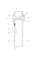
101 {100}シリコン基板
102 能動素子
103 絶縁膜
104 配線部
105 貫通孔
106 絶縁層
107 導電層
108 封止材
109 保護層
110 外部接続電極
111 開口部
Claims (2)
- 表面の結晶方位が{100}結晶面のシリコン基板の表面に、保護膜を形成し、
前記{100}結晶面のシリコン基板の表面の{111}結晶面の境界線に沿って、前記シリコン基板の表面から前記保護膜を除去して前記シリコン基板を露出させた四角形状の開口部を形成し、
前記開口部にレーザを照射して前記シリコン基板を貫通する貫通孔を形成し、
前記貫通孔を、TMAH水溶液を用いたウェットエッチングによって、前記貫通孔の断面形状が四角形状となるように拡大し、
前記貫通孔の断面形状の対角線が、前記開口部の四角形状の一辺の長さと等しくなる前に前記エッチングを終了することを特徴とする貫通孔形成方法。 - 貫通孔により表裏面が電気的に接続されている半導体装置の製造方法において、表面の結晶方位が{100}結晶面のシリコン基板の表面に、保護膜を形成し、
前記{100}結晶面のシリコン基板の表面の{111}結晶面の境界線に沿って、前記シリコン基板の表面から前記保護膜を除去して前記シリコン基板を露出させた四角形状の開口部を形成し、
前記開口部にレーザを照射して前記シリコン基板を貫通する貫通孔を形成し、
前記貫通孔を、TMAH水溶液を用いたウェットエッチングによって、前記貫通孔の断面形状が四角形状となるように拡大し、
前記貫通孔の断面形状の対角線が、前記開口部の四角形状の一辺の長さと等しくなる前に前記エッチングを終了し、
前記貫通孔の内側表面に絶縁層を形成し、前記絶縁層の内側表面に導電層を形成することで、前記シリコン基板の表裏面を電気的に接続することを特徴とする半導体装置の製造方法。
Priority Applications (4)
| Application Number | Priority Date | Filing Date | Title |
|---|---|---|---|
| JP2005141086A JP4955935B2 (ja) | 2004-05-25 | 2005-05-13 | 貫通孔形成方法および半導体装置の製造方法 |
| US11/134,427 US7279776B2 (en) | 2004-05-25 | 2005-05-23 | Method of manufacturing semiconductor device and semiconductor device |
| US11/844,822 US7821105B2 (en) | 2004-05-25 | 2007-08-24 | Method of manufacturing semiconductor device and semiconductor device |
| US11/844,811 US7713872B2 (en) | 2004-05-25 | 2007-08-24 | Method of manufacturing semiconductor device and semiconductor device |
Applications Claiming Priority (3)
| Application Number | Priority Date | Filing Date | Title |
|---|---|---|---|
| JP2004154836 | 2004-05-25 | ||
| JP2004154836 | 2004-05-25 | ||
| JP2005141086A JP4955935B2 (ja) | 2004-05-25 | 2005-05-13 | 貫通孔形成方法および半導体装置の製造方法 |
Publications (3)
| Publication Number | Publication Date |
|---|---|
| JP2006013454A JP2006013454A (ja) | 2006-01-12 |
| JP2006013454A5 JP2006013454A5 (ja) | 2008-06-26 |
| JP4955935B2 true JP4955935B2 (ja) | 2012-06-20 |
Family
ID=35425939
Family Applications (1)
| Application Number | Title | Priority Date | Filing Date |
|---|---|---|---|
| JP2005141086A Expired - Fee Related JP4955935B2 (ja) | 2004-05-25 | 2005-05-13 | 貫通孔形成方法および半導体装置の製造方法 |
Country Status (2)
| Country | Link |
|---|---|
| US (3) | US7279776B2 (ja) |
| JP (1) | JP4955935B2 (ja) |
Families Citing this family (49)
| Publication number | Priority date | Publication date | Assignee | Title |
|---|---|---|---|---|
| US8084866B2 (en) | 2003-12-10 | 2011-12-27 | Micron Technology, Inc. | Microelectronic devices and methods for filling vias in microelectronic devices |
| JP4955935B2 (ja) | 2004-05-25 | 2012-06-20 | キヤノン株式会社 | 貫通孔形成方法および半導体装置の製造方法 |
| US7083425B2 (en) | 2004-08-27 | 2006-08-01 | Micron Technology, Inc. | Slanted vias for electrical circuits on circuit boards and other substrates |
| US8278738B2 (en) * | 2005-02-17 | 2012-10-02 | Sharp Kabushiki Kaisha | Method of producing semiconductor device and semiconductor device |
| US7560813B2 (en) | 2005-06-14 | 2009-07-14 | John Trezza | Chip-based thermo-stack |
| US7851348B2 (en) * | 2005-06-14 | 2010-12-14 | Abhay Misra | Routingless chip architecture |
| US7946331B2 (en) * | 2005-06-14 | 2011-05-24 | Cufer Asset Ltd. L.L.C. | Pin-type chip tooling |
| US7781886B2 (en) | 2005-06-14 | 2010-08-24 | John Trezza | Electronic chip contact structure |
| US7767493B2 (en) * | 2005-06-14 | 2010-08-03 | John Trezza | Post & penetration interconnection |
| US8456015B2 (en) * | 2005-06-14 | 2013-06-04 | Cufer Asset Ltd. L.L.C. | Triaxial through-chip connection |
| US7786592B2 (en) * | 2005-06-14 | 2010-08-31 | John Trezza | Chip capacitive coupling |
| US20060281303A1 (en) * | 2005-06-14 | 2006-12-14 | John Trezza | Tack & fuse chip bonding |
| US20060278996A1 (en) * | 2005-06-14 | 2006-12-14 | John Trezza | Active packaging |
| US7838997B2 (en) * | 2005-06-14 | 2010-11-23 | John Trezza | Remote chip attachment |
| US7687400B2 (en) * | 2005-06-14 | 2010-03-30 | John Trezza | Side stacking apparatus and method |
| US7795134B2 (en) | 2005-06-28 | 2010-09-14 | Micron Technology, Inc. | Conductive interconnect structures and formation methods using supercritical fluids |
| US7262134B2 (en) | 2005-09-01 | 2007-08-28 | Micron Technology, Inc. | Microfeature workpieces and methods for forming interconnects in microfeature workpieces |
| US7863187B2 (en) | 2005-09-01 | 2011-01-04 | Micron Technology, Inc. | Microfeature workpieces and methods for forming interconnects in microfeature workpieces |
| US20070045120A1 (en) * | 2005-09-01 | 2007-03-01 | Micron Technology, Inc. | Methods and apparatus for filling features in microfeature workpieces |
| US8154105B2 (en) * | 2005-09-22 | 2012-04-10 | International Rectifier Corporation | Flip chip semiconductor device and process of its manufacture |
| US8138075B1 (en) | 2006-02-06 | 2012-03-20 | Eberlein Dietmar C | Systems and methods for the manufacture of flat panel devices |
| JP2007258233A (ja) * | 2006-03-20 | 2007-10-04 | Oki Electric Ind Co Ltd | 半導体装置の製造方法、半導体装置および回路基板 |
| US7749899B2 (en) * | 2006-06-01 | 2010-07-06 | Micron Technology, Inc. | Microelectronic workpieces and methods and systems for forming interconnects in microelectronic workpieces |
| US7687397B2 (en) * | 2006-06-06 | 2010-03-30 | John Trezza | Front-end processed wafer having through-chip connections |
| US20070281460A1 (en) * | 2006-06-06 | 2007-12-06 | Cubic Wafer, Inc. | Front-end processed wafer having through-chip connections |
| US7629249B2 (en) | 2006-08-28 | 2009-12-08 | Micron Technology, Inc. | Microfeature workpieces having conductive interconnect structures formed by chemically reactive processes, and associated systems and methods |
| US7902643B2 (en) | 2006-08-31 | 2011-03-08 | Micron Technology, Inc. | Microfeature workpieces having interconnects and conductive backplanes, and associated systems and methods |
| JP2008066481A (ja) * | 2006-09-06 | 2008-03-21 | Shinko Electric Ind Co Ltd | パッケージ、半導体装置、パッケージの製造方法及び半導体装置の製造方法 |
| US7670874B2 (en) * | 2007-02-16 | 2010-03-02 | John Trezza | Plated pillar package formation |
| DE102007019552B4 (de) * | 2007-04-25 | 2009-12-17 | Infineon Technologies Ag | Verfahren zur Herstellung eines Substrats mit Durchführung sowie Substrat und Halbleitermodul mit Durchführung |
| US7825517B2 (en) * | 2007-07-16 | 2010-11-02 | Taiwan Semiconductor Manufacturing Company, Ltd. | Method for packaging semiconductor dies having through-silicon vias |
| SG150410A1 (en) | 2007-08-31 | 2009-03-30 | Micron Technology Inc | Partitioned through-layer via and associated systems and methods |
| US7884015B2 (en) | 2007-12-06 | 2011-02-08 | Micron Technology, Inc. | Methods for forming interconnects in microelectronic workpieces and microelectronic workpieces formed using such methods |
| KR101002680B1 (ko) | 2008-10-21 | 2010-12-21 | 삼성전기주식회사 | 반도체 패키지 및 그 제조 방법 |
| US8330256B2 (en) * | 2008-11-18 | 2012-12-11 | Seiko Epson Corporation | Semiconductor device having through electrodes, a manufacturing method thereof, and an electronic apparatus |
| DE102008054765A1 (de) * | 2008-12-16 | 2010-06-24 | Robert Bosch Gmbh | Bauteil mit einer Durchkontaktierung und ein Verfahren zur Herstellung eines solchen Bauteils |
| JP5330863B2 (ja) * | 2009-03-04 | 2013-10-30 | パナソニック株式会社 | 半導体装置の製造方法 |
| JP5106460B2 (ja) * | 2009-03-26 | 2012-12-26 | 新光電気工業株式会社 | 半導体装置及びその製造方法、並びに電子装置 |
| US8062975B2 (en) | 2009-04-16 | 2011-11-22 | Freescale Semiconductor, Inc. | Through substrate vias |
| DE102010029760B4 (de) * | 2010-06-07 | 2019-02-21 | Robert Bosch Gmbh | Bauelement mit einer Durchkontaktierung und Verfahren zu seiner Herstellung |
| JP5730654B2 (ja) * | 2010-06-24 | 2015-06-10 | 新光電気工業株式会社 | 配線基板及びその製造方法 |
| EP2600397B1 (en) * | 2010-07-26 | 2019-08-21 | Hamamatsu Photonics K.K. | Method for manufacturing interposer |
| JP2012256679A (ja) | 2011-06-08 | 2012-12-27 | Elpida Memory Inc | 半導体装置及びその製造方法 |
| JP2013161910A (ja) * | 2012-02-03 | 2013-08-19 | Osaka Prefecture Univ | 半導体装置の製造方法、半導体装置、赤外線センサの製造方法および赤外線センサ |
| US20140151895A1 (en) * | 2012-12-05 | 2014-06-05 | Texas Instruments Incorporated | Die having through-substrate vias with deformation protected tips |
| JP6033130B2 (ja) * | 2013-03-13 | 2016-11-30 | 新光電気工業株式会社 | プローブガイド板及びその製造方法 |
| JP6235785B2 (ja) * | 2013-03-18 | 2017-11-22 | 日本電子材料株式会社 | プローブカード用ガイド板およびプローブカード用ガイド板の製造方法 |
| JP2015002299A (ja) * | 2013-06-17 | 2015-01-05 | 株式会社ザイキューブ | 漏斗状の貫通電極およびその製造方法 |
| JP7230650B2 (ja) * | 2019-04-05 | 2023-03-01 | Tdk株式会社 | 無機材料基板の加工方法、デバイス、およびデバイスの製造方法 |
Family Cites Families (14)
| Publication number | Priority date | Publication date | Assignee | Title |
|---|---|---|---|---|
| US4961821A (en) * | 1989-11-22 | 1990-10-09 | Xerox Corporation | Ode through holes and butt edges without edge dicing |
| JPH03253025A (ja) * | 1990-03-02 | 1991-11-12 | Nippon Telegr & Teleph Corp <Ntt> | 加工基板及びシリコン異方性エッチング方法 |
| JPH04299872A (ja) * | 1991-03-28 | 1992-10-23 | Yokogawa Electric Corp | シリコンダイアフラムの形成方法 |
| JPH05243207A (ja) * | 1991-05-13 | 1993-09-21 | Jeol Ltd | シリコンウエハーの加工方法 |
| JP2000246474A (ja) * | 1999-02-25 | 2000-09-12 | Seiko Epson Corp | レーザ光による加工方法 |
| US6563079B1 (en) * | 1999-02-25 | 2003-05-13 | Seiko Epson Corporation | Method for machining work by laser beam |
| JP2001135785A (ja) * | 1999-11-08 | 2001-05-18 | Seiko Epson Corp | 半導体チップ、マルチチップパッケージ、半導体装置、および電子機器、並びにこれらの製造方法 |
| JP3736607B2 (ja) * | 2000-01-21 | 2006-01-18 | セイコーエプソン株式会社 | 半導体装置及びその製造方法、回路基板並びに電子機器 |
| JP3879816B2 (ja) * | 2000-06-02 | 2007-02-14 | セイコーエプソン株式会社 | 半導体装置及びその製造方法、積層型半導体装置、回路基板並びに電子機器 |
| JP2002094082A (ja) * | 2000-07-11 | 2002-03-29 | Seiko Epson Corp | 光素子及びその製造方法並びに電子機器 |
| JP3669487B2 (ja) * | 2001-01-19 | 2005-07-06 | 株式会社フジクラ | 光励起電解研磨法による貫通孔形成方法 |
| JP2002359347A (ja) * | 2001-03-28 | 2002-12-13 | Seiko Epson Corp | 半導体装置及びその製造方法、回路基板並びに電子機器 |
| US7494925B2 (en) * | 2004-02-23 | 2009-02-24 | Micron Technology, Inc. | Method for making through-hole conductors for semiconductor substrates |
| JP4955935B2 (ja) | 2004-05-25 | 2012-06-20 | キヤノン株式会社 | 貫通孔形成方法および半導体装置の製造方法 |
-
2005
- 2005-05-13 JP JP2005141086A patent/JP4955935B2/ja not_active Expired - Fee Related
- 2005-05-23 US US11/134,427 patent/US7279776B2/en not_active Expired - Fee Related
-
2007
- 2007-08-24 US US11/844,811 patent/US7713872B2/en not_active Expired - Fee Related
- 2007-08-24 US US11/844,822 patent/US7821105B2/en not_active Expired - Fee Related
Also Published As
| Publication number | Publication date |
|---|---|
| US7821105B2 (en) | 2010-10-26 |
| US7713872B2 (en) | 2010-05-11 |
| US7279776B2 (en) | 2007-10-09 |
| JP2006013454A (ja) | 2006-01-12 |
| US20050266687A1 (en) | 2005-12-01 |
| US20080003817A1 (en) | 2008-01-03 |
| US20080001299A1 (en) | 2008-01-03 |
Similar Documents
| Publication | Publication Date | Title |
|---|---|---|
| JP4955935B2 (ja) | 貫通孔形成方法および半導体装置の製造方法 | |
| JP4323303B2 (ja) | 基板の製造方法 | |
| CA2539280C (en) | High reliability multilayer circuit substrates and methods for their formation | |
| JPH04290232A (ja) | 溝埋込み配線形成方法 | |
| JP2008066481A (ja) | パッケージ、半導体装置、パッケージの製造方法及び半導体装置の製造方法 | |
| KR20090024640A (ko) | 반도체 장치 및 반도체 장치의 제조 방법 | |
| TWI534068B (zh) | 製造構件的方法與製造構件裝置的方法,以及構件和構件裝置 | |
| JP5046819B2 (ja) | スルーホールの形成方法およびインクジェットヘッド | |
| JP4069028B2 (ja) | 貫通電極付き基板、その製造方法及び電子デバイス | |
| US6875365B2 (en) | Method for producing liquid discharge head | |
| JP4979793B2 (ja) | 液体吐出ヘッド用基板の製造方法 | |
| US6818138B2 (en) | Slotted substrate and slotting process | |
| JP4795102B2 (ja) | 配線基板およびその製造方法 | |
| US6524949B2 (en) | Method of forming low-resistance contact electrodes in semiconductor devices | |
| JP4217434B2 (ja) | スルーホールの形成方法及びこれを用いたインクジェットヘッド | |
| JP2004119593A (ja) | 半導体装置の製造方法 | |
| JP2751181B2 (ja) | 半導体装置の製法 | |
| JP2005093954A (ja) | 貫通電極付き基板、その製造方法及び電子デバイス | |
| TWI781384B (zh) | 對氧化矽-氮化矽-氧化矽堆疊進行圖案化的方法及由其形成的結構 | |
| JP5407316B2 (ja) | 半導体装置の製造方法 | |
| JP2874216B2 (ja) | 半導体装置およびその製造方法 | |
| JP2006224603A (ja) | インクジェット記録ヘッド | |
| JP2006216747A (ja) | 貫通電極の製造方法および構造 | |
| JP2001144174A (ja) | 誘電体分離基板の製造方法 | |
| JP5274694B2 (ja) | スルーホールの形成方法、インクジェットヘッド及びシリコン基板 |
Legal Events
| Date | Code | Title | Description |
|---|---|---|---|
| A521 | Written amendment |
Free format text: JAPANESE INTERMEDIATE CODE: A523 Effective date: 20080513 |
|
| A621 | Written request for application examination |
Free format text: JAPANESE INTERMEDIATE CODE: A621 Effective date: 20080513 |
|
| RD04 | Notification of resignation of power of attorney |
Free format text: JAPANESE INTERMEDIATE CODE: A7424 Effective date: 20100201 |
|
| RD01 | Notification of change of attorney |
Free format text: JAPANESE INTERMEDIATE CODE: A7421 Effective date: 20100630 |
|
| A977 | Report on retrieval |
Free format text: JAPANESE INTERMEDIATE CODE: A971007 Effective date: 20110608 |
|
| A131 | Notification of reasons for refusal |
Free format text: JAPANESE INTERMEDIATE CODE: A131 Effective date: 20110628 |
|
| A521 | Written amendment |
Free format text: JAPANESE INTERMEDIATE CODE: A523 Effective date: 20110822 |
|
| A131 | Notification of reasons for refusal |
Free format text: JAPANESE INTERMEDIATE CODE: A131 Effective date: 20110920 |
|
| A521 | Written amendment |
Free format text: JAPANESE INTERMEDIATE CODE: A523 Effective date: 20111121 |
|
| TRDD | Decision of grant or rejection written | ||
| A01 | Written decision to grant a patent or to grant a registration (utility model) |
Free format text: JAPANESE INTERMEDIATE CODE: A01 Effective date: 20120313 |
|
| A01 | Written decision to grant a patent or to grant a registration (utility model) |
Free format text: JAPANESE INTERMEDIATE CODE: A01 |
|
| A61 | First payment of annual fees (during grant procedure) |
Free format text: JAPANESE INTERMEDIATE CODE: A61 Effective date: 20120316 |
|
| FPAY | Renewal fee payment (event date is renewal date of database) |
Free format text: PAYMENT UNTIL: 20150323 Year of fee payment: 3 |
|
| LAPS | Cancellation because of no payment of annual fees |