JP6033130B2 - プローブガイド板及びその製造方法 - Google Patents
プローブガイド板及びその製造方法 Download PDFInfo
- Publication number
- JP6033130B2 JP6033130B2 JP2013050078A JP2013050078A JP6033130B2 JP 6033130 B2 JP6033130 B2 JP 6033130B2 JP 2013050078 A JP2013050078 A JP 2013050078A JP 2013050078 A JP2013050078 A JP 2013050078A JP 6033130 B2 JP6033130 B2 JP 6033130B2
- Authority
- JP
- Japan
- Prior art keywords
- substrate
- probe
- hole
- guide plate
- main surface
- Prior art date
- Legal status (The legal status is an assumption and is not a legal conclusion. Google has not performed a legal analysis and makes no representation as to the accuracy of the status listed.)
- Active
Links
Images


Classifications
-
- G—PHYSICS
- G01—MEASURING; TESTING
- G01R—MEASURING ELECTRIC VARIABLES; MEASURING MAGNETIC VARIABLES
- G01R1/00—Details of instruments or arrangements of the types included in groups G01R5/00 - G01R13/00 and G01R31/00
- G01R1/02—General constructional details
- G01R1/06—Measuring leads; Measuring probes
- G01R1/067—Measuring probes
- G01R1/073—Multiple probes
- G01R1/07307—Multiple probes with individual probe elements, e.g. needles, cantilever beams or bump contacts, fixed in relation to each other, e.g. bed of nails fixture or probe card
- G01R1/07357—Multiple probes with individual probe elements, e.g. needles, cantilever beams or bump contacts, fixed in relation to each other, e.g. bed of nails fixture or probe card with flexible bodies, e.g. buckling beams
-
- G—PHYSICS
- G01—MEASURING; TESTING
- G01R—MEASURING ELECTRIC VARIABLES; MEASURING MAGNETIC VARIABLES
- G01R1/00—Details of instruments or arrangements of the types included in groups G01R5/00 - G01R13/00 and G01R31/00
- G01R1/02—General constructional details
- G01R1/06—Measuring leads; Measuring probes
- G01R1/067—Measuring probes
- G01R1/073—Multiple probes
- G01R1/07307—Multiple probes with individual probe elements, e.g. needles, cantilever beams or bump contacts, fixed in relation to each other, e.g. bed of nails fixture or probe card
- G01R1/07364—Multiple probes with individual probe elements, e.g. needles, cantilever beams or bump contacts, fixed in relation to each other, e.g. bed of nails fixture or probe card with provisions for altering position, number or connection of probe tips; Adapting to differences in pitch
- G01R1/07371—Multiple probes with individual probe elements, e.g. needles, cantilever beams or bump contacts, fixed in relation to each other, e.g. bed of nails fixture or probe card with provisions for altering position, number or connection of probe tips; Adapting to differences in pitch using an intermediate card or back card with apertures through which the probes pass
Description
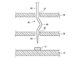
まず、半導体試験装置について図1を用いて説明する。図1は半導体試験装置の概略を示す図であり、図2はプローブを示す図である。
(プローブガイド板)
第1実施形態によるプローブガイド板について図3を用いて説明する。図3(a)は本実施形態によるプローブガイド板のA−A′線断面図であり、図3(b)は本実施形態によるプローブガイド板の平面図である。
第1実施形態によるプローブガイド板の一製造方法について図4乃至図6を用いて説明する。図4乃至図6は第1実施形態によるプローブガイド板の一製造方法を示す工程断面図である。
第1実施形態によるプローブガイド板の他の製造方法について図7及び図8を用いて説明する。図7及び図8は第1実施形態によるプローブガイド板の他の製造方法を示す工程断面図である。
(プローブガイド板)
第2実施形態によるプローブガイド板について図9を用いて説明する。図9(a)は本実施形態によるプローブガイド板のB−B′線断面図であり、図9(b)は本実施形態によるプローブガイド板の平面図である。なお、第1実施形態と同様の構成要素には同様な符号を付して説明を省略又は簡略にする。
第2実施形態によるプローブガイド板の一製造方法について図10及び図11を用いて説明する。図10及び図11は第2実施形態によるプローブガイド板の一製造方法を示す工程断面図である。なお、第1実施形態と同様の構成要素には同様な符号を付して説明を省略又は簡略にする。
第2実施形態によるプローブガイド板の他の製造方法について図12を用いて説明する。図12は第2実施形態によるプローブガイド板の他の製造方法を示す工程断面図である。なお、第1実施形態と同様の構成要素には同様な符号を付して説明を省略又は簡略にする。
(プローブガイド板)
第3実施形態によるプローブガイド板について図13を用いて説明する。図13(a)は本実施形態によるプローブガイド板のC−C′線断面図であり、図13(b)は本実施形態によるプローブガイド板の平面図である。なお、第1実施形態及び第2実施形態と同様の構成要素には同様な符号を付して説明を省略又は簡略にする。
第3実施形態によるプローブガイド板の一製造方法について図14乃至図15を用いて説明する。図14乃至図15は第3実施形態によるプローブガイド板の一製造方法を示す工程断面図である。なお、第1実施形態及び第2実施形態と同様の構成要素には同様な符号を付して説明を省略又は簡略にする。
第3実施形態によるプローブガイド板の他の製造方法について図16を用いて説明する。図16は第3実施形態によるプローブガイド板の他の製造方法を示す工程断面図である。なお、第1実施形態及び第2実施形態と同様の構成要素には同様な符号を付して説明を省略又は簡略にする。
上記実施形態は一例であって、必要に応じて種々の変形が可能である。
12…テスタ
14…検査対象物
15…電極
16…インターポーザ基板
17…電極
20…プローブ装置
22…配線基板
24…配線
26…電極
28…電極
30…ハウジング
32…ホルダ
34…セラミック基板
36、38…プローブガイド板
37、39…貫通孔
40…プローブ
42…根元部
44…先端部
46…屈曲部
50…プローブガイド板
52…基板
54…貫通孔
55…近傍領域
56…絶縁膜
60…レジスト
62…開口
64…非貫通孔
66…シリコン酸化膜
68、70…レジスト
72…シリコン窒化膜
74…シリコン酸化膜
76…フォトレジスト膜
78…シリコン酸化膜
80…絶縁膜(シリコン酸化膜)
82…絶縁膜(シリコン酸化膜)
84…埋め込み部材
90…シリコン窒化膜
92、94…レジスト
93、95…開口
Claims (8)
- プローブをガイドするための貫通孔が形成されたシリコン基板と、
前記シリコン基板の前記貫通孔の内壁と、前記シリコン基板の第1の主面における前記貫通孔の近傍領域と、前記シリコン基板の前記第1の主面の反対側の第2の主面における前記貫通孔の近傍領域とに選択的に形成された第1のシリコン酸化膜と
を有することを特徴とするプローブガイド板。 - プローブをガイドするための貫通孔が形成されたシリコン基板と、
前記シリコン基板の前記貫通孔の内壁に選択的に形成された第1のシリコン酸化膜と、
前記シリコン基板の第1の主面と、前記シリコン基板の前記第1の主面の反対側の第2の主面とに形成され、前記第1のシリコン酸化膜よりも膜厚の薄い第2のシリコン酸化膜と
を有することを特徴とするプローブガイド板。 - 請求項1又は2に記載のプローブガイド板において、
前記第1のシリコン酸化膜の膜厚は、3μm〜10μmである
ことを特徴とするプローブガイド板。 - 請求項1乃至3のいずれか1項に記載のプローブガイド板を有することを特徴とするプローブ装置。
- 基板に、プローブをガイドするための貫通孔を形成する工程と、
前記基板の前記貫通孔の内壁と、前記基板の第1の主面と、前記基板の前記第1の主面の反対側の第2の主面とに、第1の絶縁膜を形成する工程と、
前記基板の前記第1の主面に形成された前記第1の絶縁膜のうちの前記貫通孔の近傍領域以外の部分、及び、前記基板の前記第2の主面に形成された前記第1の絶縁膜のうちの前記貫通孔の近傍領域以外の部分をエッチング除去する工程と
を有することを特徴とするプローブガイド板の製造方法。 - 基板に、プローブをガイドするための貫通孔を形成する工程と、
前記基板の前記貫通孔と、前記基板の第1の主面における前記貫通孔の近傍領域と、前記基板の前記第1の主面の反対側の第2の主面における前記貫通孔の近傍領域とを露出するマスク層を形成する工程と、
前記マスク層をマスクとして、前記基板の前記貫通孔の内壁と、前記基板の前記第1の主面における前記貫通孔の前記近傍領域と、前記基板の前記第2の主面における前記貫通孔の前記近傍領域とに、第1の絶縁膜を形成する工程と
を有することを特徴とするプローブガイド板の製造方法。 - 基板に、プローブをガイドするための貫通孔を形成する工程と、
前記基板の前記貫通孔の内壁と、前記基板の第1の主面と、前記基板の前記第1の主面の反対側の第2の主面とに、第1の絶縁膜を形成する工程と、
前記第1の絶縁膜のうちの前記第1の主面に形成された部分、及び、前記第1の絶縁膜のうちの前記第2の主面に形成された部分を、薄くする工程と
を有することを特徴とするプローブガイド板の製造方法。 - 請求項7記載のプローブガイド板の製造方法において、
前記第1の絶縁膜を形成する工程の後に、前記内壁に前記第1の絶縁膜が形成された前記貫通孔内に、前記第1の絶縁膜とエッチング特性が異なる部材を埋め込む工程を更に有し、
前記薄くする工程は、前記第1の絶縁膜をエッチングすることにより前記第1の絶縁膜を薄くする
ことを特徴とするプローブガイド板の製造方法。
Priority Applications (4)
| Application Number | Priority Date | Filing Date | Title |
|---|---|---|---|
| JP2013050078A JP6033130B2 (ja) | 2013-03-13 | 2013-03-13 | プローブガイド板及びその製造方法 |
| KR1020140022332A KR102090102B1 (ko) | 2013-03-13 | 2014-02-26 | 프로브 가이드판 및 그 제조 방법 |
| US14/202,701 US9523716B2 (en) | 2013-03-13 | 2014-03-10 | Probe guide plate and method for manufacturing the same |
| TW103108624A TWI625529B (zh) | 2013-03-13 | 2014-03-12 | 探針導孔板及其製造方法 |
Applications Claiming Priority (1)
| Application Number | Priority Date | Filing Date | Title |
|---|---|---|---|
| JP2013050078A JP6033130B2 (ja) | 2013-03-13 | 2013-03-13 | プローブガイド板及びその製造方法 |
Publications (3)
| Publication Number | Publication Date |
|---|---|
| JP2014174145A JP2014174145A (ja) | 2014-09-22 |
| JP2014174145A5 JP2014174145A5 (ja) | 2016-02-04 |
| JP6033130B2 true JP6033130B2 (ja) | 2016-11-30 |
Family
ID=51524807
Family Applications (1)
| Application Number | Title | Priority Date | Filing Date |
|---|---|---|---|
| JP2013050078A Active JP6033130B2 (ja) | 2013-03-13 | 2013-03-13 | プローブガイド板及びその製造方法 |
Country Status (4)
| Country | Link |
|---|---|
| US (1) | US9523716B2 (ja) |
| JP (1) | JP6033130B2 (ja) |
| KR (1) | KR102090102B1 (ja) |
| TW (1) | TWI625529B (ja) |
Families Citing this family (12)
| Publication number | Priority date | Publication date | Assignee | Title |
|---|---|---|---|---|
| JP6235785B2 (ja) | 2013-03-18 | 2017-11-22 | 日本電子材料株式会社 | プローブカード用ガイド板およびプローブカード用ガイド板の製造方法 |
| CN105093000B (zh) * | 2014-05-19 | 2019-03-15 | 鸿富锦精密电子(郑州)有限公司 | 测试装置 |
| JP6233331B2 (ja) * | 2015-02-27 | 2017-11-22 | トヨタ自動車株式会社 | 半導体基板の温度検査方法、半導体装置の製造方法及び半導体基板の温度検査装置 |
| TWI702402B (zh) * | 2015-05-07 | 2020-08-21 | 義大利商探針科技公司 | 特別用於減少間距應用的具有垂直探針的測試頭 |
| JP6563317B2 (ja) * | 2015-11-25 | 2019-08-21 | 新光電気工業株式会社 | プローブガイド板及びその製造方法とプローブ装置 |
| JP6654061B2 (ja) | 2016-02-23 | 2020-02-26 | 日本電子材料株式会社 | プローブガイド、プローブカード及びプローブガイドの製造方法 |
| JP6855185B2 (ja) * | 2016-07-27 | 2021-04-07 | 株式会社日本マイクロニクス | 電気的接続装置 |
| JP2017201321A (ja) * | 2017-06-29 | 2017-11-09 | 日本電子材料株式会社 | プローブカード用ガイド板およびプローブカード用ガイド板の製造方法 |
| TWI666451B (zh) * | 2017-09-15 | 2019-07-21 | 中華精測科技股份有限公司 | 探針裝置及其導板 |
| WO2022024888A1 (ja) * | 2020-07-27 | 2022-02-03 | 京セラ株式会社 | プローブガイド |
| KR20230165258A (ko) * | 2021-03-23 | 2023-12-05 | 닐슨 싸이언티픽, 엘엘씨 | 극저온 프로브 카드 |
| TWI798069B (zh) * | 2022-04-26 | 2023-04-01 | 寶虹科技股份有限公司 | 探針卡 |
Family Cites Families (25)
| Publication number | Priority date | Publication date | Assignee | Title |
|---|---|---|---|---|
| JP3350638B2 (ja) * | 1997-06-26 | 2002-11-25 | 沖電気工業株式会社 | 半導体素子の製造方法 |
| KR20010021666A (ko) * | 1997-07-14 | 2001-03-15 | 마에다 츠구요시 | 도전성 접촉자 |
| KR100379350B1 (ko) * | 1998-12-16 | 2003-04-08 | 세이코 엡슨 가부시키가이샤 | 반도체 칩, 반도체 장치, 회로 기판 및 전자기기 및 그제조 방법 |
| CN1200793C (zh) * | 1999-02-25 | 2005-05-11 | 精工爱普生株式会社 | 利用激光加工被加工物的方法 |
| JP4690556B2 (ja) * | 2000-07-21 | 2011-06-01 | 大日本印刷株式会社 | 微細パターン形成装置と微細ノズルの製造方法 |
| JP2002296297A (ja) | 2001-03-29 | 2002-10-09 | Isao Kimoto | 接触子組立体 |
| KR20040089244A (ko) | 2003-04-11 | 2004-10-21 | 주식회사 유림하이테크산업 | 프로브 카드의 니들 어셈블리 |
| JP4955935B2 (ja) * | 2004-05-25 | 2012-06-20 | キヤノン株式会社 | 貫通孔形成方法および半導体装置の製造方法 |
| JP4698296B2 (ja) * | 2005-06-17 | 2011-06-08 | 新光電気工業株式会社 | 貫通電極を有する半導体装置の製造方法 |
| TWI261933B (en) * | 2005-11-21 | 2006-09-11 | Mjc Probe Inc | Method for batch production process of micro-hole guide plate of vertical probe card |
| JP2007171139A (ja) * | 2005-12-26 | 2007-07-05 | Apex Inc | プローブ保持構造およびバネ型プローブ |
| JP2007171140A (ja) * | 2005-12-26 | 2007-07-05 | Apex Inc | プローブカード、インターポーザおよびインターポーザの製造方法 |
| TWI284209B (en) * | 2005-12-30 | 2007-07-21 | Ind Tech Res Inst | A method of fabricating vertical probe head |
| JP2007201361A (ja) * | 2006-01-30 | 2007-08-09 | Shinko Electric Ind Co Ltd | 半導体装置及び半導体装置の製造方法 |
| JP4703456B2 (ja) * | 2006-03-28 | 2011-06-15 | 大日本印刷株式会社 | 電気信号測定用治具 |
| JP2007263649A (ja) * | 2006-03-28 | 2007-10-11 | Dainippon Printing Co Ltd | 電気信号計測用治具およびその製造方法 |
| TWI352440B (en) * | 2007-10-16 | 2011-11-11 | Silicon Base Dev Inc | Package base structure of light diode and manufact |
| JPWO2009104589A1 (ja) * | 2008-02-21 | 2011-06-23 | 東京エレクトロン株式会社 | プローブ支持板の製造方法、コンピュータ記憶媒体及びプローブ支持板 |
| KR100973413B1 (ko) * | 2008-09-04 | 2010-08-03 | 이용준 | 반도체 소자 테스트용 콘택터 |
| JP5386769B2 (ja) * | 2008-09-29 | 2014-01-15 | 日本電産リード株式会社 | 検査治具 |
| JP5367616B2 (ja) * | 2009-02-23 | 2013-12-11 | 新光電気工業株式会社 | 配線基板及びその製造方法 |
| JP5379065B2 (ja) * | 2010-04-21 | 2013-12-25 | 新光電気工業株式会社 | プローブカード及びその製造方法 |
| US8723538B2 (en) * | 2011-06-17 | 2014-05-13 | Taiwan Semiconductor Manufacturing Company, Ltd. | Probe head formation methods employing guide plate raising assembly mechanism |
| JP5847663B2 (ja) | 2012-08-01 | 2016-01-27 | 日本電子材料株式会社 | プローブカード用ガイド板の製造方法 |
| JP6235785B2 (ja) | 2013-03-18 | 2017-11-22 | 日本電子材料株式会社 | プローブカード用ガイド板およびプローブカード用ガイド板の製造方法 |
-
2013
- 2013-03-13 JP JP2013050078A patent/JP6033130B2/ja active Active
-
2014
- 2014-02-26 KR KR1020140022332A patent/KR102090102B1/ko active IP Right Grant
- 2014-03-10 US US14/202,701 patent/US9523716B2/en active Active
- 2014-03-12 TW TW103108624A patent/TWI625529B/zh active
Also Published As
| Publication number | Publication date |
|---|---|
| US9523716B2 (en) | 2016-12-20 |
| JP2014174145A (ja) | 2014-09-22 |
| TW201447308A (zh) | 2014-12-16 |
| KR20140112396A (ko) | 2014-09-23 |
| TWI625529B (zh) | 2018-06-01 |
| KR102090102B1 (ko) | 2020-03-17 |
| US20140266274A1 (en) | 2014-09-18 |
Similar Documents
| Publication | Publication Date | Title |
|---|---|---|
| JP6033130B2 (ja) | プローブガイド板及びその製造方法 | |
| JP6654061B2 (ja) | プローブガイド、プローブカード及びプローブガイドの製造方法 | |
| JP6235785B2 (ja) | プローブカード用ガイド板およびプローブカード用ガイド板の製造方法 | |
| JP6341634B2 (ja) | プローブガイド板及びその製造方法、半導体検査装置 | |
| US7129156B2 (en) | Method for fabricating a silicon carbide interconnect for semiconductor components using heating | |
| JP6563317B2 (ja) | プローブガイド板及びその製造方法とプローブ装置 | |
| US6563215B1 (en) | Silicon carbide interconnect for semiconductor components and method of fabrication | |
| JP2009276316A (ja) | プローブカード | |
| JP6872960B2 (ja) | 電気的接続装置 | |
| KR20100048673A (ko) | 프로브 구조물 및 프로브 구조물 제조 방법 | |
| JP2007173325A (ja) | 半導体装置の製造方法 | |
| JP3379699B2 (ja) | プローバの製造方法 | |
| JP4967907B2 (ja) | 半導体圧力センサ及びその製造方法 | |
| KR100745108B1 (ko) | 프로브 카드의 실리콘 기판 | |
| US6975030B1 (en) | Silicon carbide contact for semiconductor components | |
| KR20080109270A (ko) | 프로브 카드 제조 방법 | |
| JP2004195052A (ja) | 多点微小電極、生体電位計測用デバイス、多点微小電極の作製方法、及び生体電位計測用デバイスの作製方法 | |
| JP5649479B2 (ja) | インプリントモールドの製造方法、インプリントモールド、及び配線板 | |
| KR100977166B1 (ko) | 니들형 탐침 제조 방법 | |
| KR101301740B1 (ko) | 프로브 카드 제조 방법 및 그에 의한 프로브 카드 | |
| JP2006194740A (ja) | プローブエレメント及びその製造方法 | |
| JP2013117511A (ja) | 基板及びその製造方法、並びにプローブカード | |
| JP2007132847A (ja) | プローブユニット及びその製造方法 | |
| KR20080111654A (ko) | 프로브 카드 및 그 제조방법 | |
| KR100743978B1 (ko) | 프로브 카드용 접촉 소자 및 그 제조 방법 |
Legal Events
| Date | Code | Title | Description |
|---|---|---|---|
| A711 | Notification of change in applicant |
Free format text: JAPANESE INTERMEDIATE CODE: A711 Effective date: 20141215 |
|
| A521 | Request for written amendment filed |
Free format text: JAPANESE INTERMEDIATE CODE: A821 Effective date: 20141215 |
|
| A521 | Request for written amendment filed |
Free format text: JAPANESE INTERMEDIATE CODE: A523 Effective date: 20151214 |
|
| A621 | Written request for application examination |
Free format text: JAPANESE INTERMEDIATE CODE: A621 Effective date: 20151214 |
|
| A977 | Report on retrieval |
Free format text: JAPANESE INTERMEDIATE CODE: A971007 Effective date: 20161006 |
|
| TRDD | Decision of grant or rejection written | ||
| A01 | Written decision to grant a patent or to grant a registration (utility model) |
Free format text: JAPANESE INTERMEDIATE CODE: A01 Effective date: 20161011 |
|
| A61 | First payment of annual fees (during grant procedure) |
Free format text: JAPANESE INTERMEDIATE CODE: A61 Effective date: 20161025 |
|
| R150 | Certificate of patent or registration of utility model |
Ref document number: 6033130 Country of ref document: JP Free format text: JAPANESE INTERMEDIATE CODE: R150 |
|
| R250 | Receipt of annual fees |
Free format text: JAPANESE INTERMEDIATE CODE: R250 |
|
| R250 | Receipt of annual fees |
Free format text: JAPANESE INTERMEDIATE CODE: R250 |
|
| R250 | Receipt of annual fees |
Free format text: JAPANESE INTERMEDIATE CODE: R250 |
|
| R250 | Receipt of annual fees |
Free format text: JAPANESE INTERMEDIATE CODE: R250 |
|
| R250 | Receipt of annual fees |
Free format text: JAPANESE INTERMEDIATE CODE: R250 |