JP4902558B2 - 半導体モジュールの製造方法 - Google Patents
半導体モジュールの製造方法 Download PDFInfo
- Publication number
- JP4902558B2 JP4902558B2 JP2008012240A JP2008012240A JP4902558B2 JP 4902558 B2 JP4902558 B2 JP 4902558B2 JP 2008012240 A JP2008012240 A JP 2008012240A JP 2008012240 A JP2008012240 A JP 2008012240A JP 4902558 B2 JP4902558 B2 JP 4902558B2
- Authority
- JP
- Japan
- Prior art keywords
- protrusion
- metal plate
- semiconductor
- copper plate
- main surface
- Prior art date
- Legal status (The legal status is an assumption and is not a legal conclusion. Google has not performed a legal analysis and makes no representation as to the accuracy of the status listed.)
- Expired - Fee Related
Links
Images


Classifications
-
- H—ELECTRICITY
- H01—ELECTRIC ELEMENTS
- H01L—SEMICONDUCTOR DEVICES NOT COVERED BY CLASS H10
- H01L21/00—Processes or apparatus adapted for the manufacture or treatment of semiconductor or solid state devices or of parts thereof
- H01L21/02—Manufacture or treatment of semiconductor devices or of parts thereof
- H01L21/04—Manufacture or treatment of semiconductor devices or of parts thereof the devices having at least one potential-jump barrier or surface barrier, e.g. PN junction, depletion layer or carrier concentration layer
- H01L21/48—Manufacture or treatment of parts, e.g. containers, prior to assembly of the devices, using processes not provided for in a single one of the subgroups H01L21/06 - H01L21/326
- H01L21/4814—Conductive parts
- H01L21/4821—Flat leads, e.g. lead frames with or without insulating supports
- H01L21/4828—Etching
- H01L21/4832—Etching a temporary substrate after encapsulation process to form leads
-
- H—ELECTRICITY
- H01—ELECTRIC ELEMENTS
- H01L—SEMICONDUCTOR DEVICES NOT COVERED BY CLASS H10
- H01L21/00—Processes or apparatus adapted for the manufacture or treatment of semiconductor or solid state devices or of parts thereof
- H01L21/02—Manufacture or treatment of semiconductor devices or of parts thereof
- H01L21/04—Manufacture or treatment of semiconductor devices or of parts thereof the devices having at least one potential-jump barrier or surface barrier, e.g. PN junction, depletion layer or carrier concentration layer
- H01L21/48—Manufacture or treatment of parts, e.g. containers, prior to assembly of the devices, using processes not provided for in a single one of the subgroups H01L21/06 - H01L21/326
- H01L21/4814—Conductive parts
- H01L21/4821—Flat leads, e.g. lead frames with or without insulating supports
- H01L21/4828—Etching
-
- H—ELECTRICITY
- H01—ELECTRIC ELEMENTS
- H01L—SEMICONDUCTOR DEVICES NOT COVERED BY CLASS H10
- H01L21/00—Processes or apparatus adapted for the manufacture or treatment of semiconductor or solid state devices or of parts thereof
- H01L21/02—Manufacture or treatment of semiconductor devices or of parts thereof
- H01L21/04—Manufacture or treatment of semiconductor devices or of parts thereof the devices having at least one potential-jump barrier or surface barrier, e.g. PN junction, depletion layer or carrier concentration layer
- H01L21/50—Assembly of semiconductor devices using processes or apparatus not provided for in a single one of the subgroups H01L21/06 - H01L21/326, e.g. sealing of a cap to a base of a container
- H01L21/56—Encapsulations, e.g. encapsulation layers, coatings
- H01L21/561—Batch processing
-
- H—ELECTRICITY
- H01—ELECTRIC ELEMENTS
- H01L—SEMICONDUCTOR DEVICES NOT COVERED BY CLASS H10
- H01L24/00—Arrangements for connecting or disconnecting semiconductor or solid-state bodies; Methods or apparatus related thereto
- H01L24/01—Means for bonding being attached to, or being formed on, the surface to be connected, e.g. chip-to-package, die-attach, "first-level" interconnects; Manufacturing methods related thereto
- H01L24/02—Bonding areas ; Manufacturing methods related thereto
-
- H—ELECTRICITY
- H01—ELECTRIC ELEMENTS
- H01L—SEMICONDUCTOR DEVICES NOT COVERED BY CLASS H10
- H01L24/00—Arrangements for connecting or disconnecting semiconductor or solid-state bodies; Methods or apparatus related thereto
- H01L24/93—Batch processes
- H01L24/94—Batch processes at wafer-level, i.e. with connecting carried out on a wafer comprising a plurality of undiced individual devices
-
- H—ELECTRICITY
- H01—ELECTRIC ELEMENTS
- H01L—SEMICONDUCTOR DEVICES NOT COVERED BY CLASS H10
- H01L24/00—Arrangements for connecting or disconnecting semiconductor or solid-state bodies; Methods or apparatus related thereto
- H01L24/93—Batch processes
- H01L24/95—Batch processes at chip-level, i.e. with connecting carried out on a plurality of singulated devices, i.e. on diced chips
- H01L24/97—Batch processes at chip-level, i.e. with connecting carried out on a plurality of singulated devices, i.e. on diced chips the devices being connected to a common substrate, e.g. interposer, said common substrate being separable into individual assemblies after connecting
-
- H—ELECTRICITY
- H01—ELECTRIC ELEMENTS
- H01L—SEMICONDUCTOR DEVICES NOT COVERED BY CLASS H10
- H01L2224/00—Indexing scheme for arrangements for connecting or disconnecting semiconductor or solid-state bodies and methods related thereto as covered by H01L24/00
- H01L2224/01—Means for bonding being attached to, or being formed on, the surface to be connected, e.g. chip-to-package, die-attach, "first-level" interconnects; Manufacturing methods related thereto
- H01L2224/02—Bonding areas; Manufacturing methods related thereto
- H01L2224/023—Redistribution layers [RDL] for bonding areas
- H01L2224/0231—Manufacturing methods of the redistribution layers
- H01L2224/02319—Manufacturing methods of the redistribution layers by using a preform
-
- H—ELECTRICITY
- H01—ELECTRIC ELEMENTS
- H01L—SEMICONDUCTOR DEVICES NOT COVERED BY CLASS H10
- H01L2224/00—Indexing scheme for arrangements for connecting or disconnecting semiconductor or solid-state bodies and methods related thereto as covered by H01L24/00
- H01L2224/01—Means for bonding being attached to, or being formed on, the surface to be connected, e.g. chip-to-package, die-attach, "first-level" interconnects; Manufacturing methods related thereto
- H01L2224/02—Bonding areas; Manufacturing methods related thereto
- H01L2224/023—Redistribution layers [RDL] for bonding areas
- H01L2224/0235—Shape of the redistribution layers
-
- H—ELECTRICITY
- H01—ELECTRIC ELEMENTS
- H01L—SEMICONDUCTOR DEVICES NOT COVERED BY CLASS H10
- H01L2224/00—Indexing scheme for arrangements for connecting or disconnecting semiconductor or solid-state bodies and methods related thereto as covered by H01L24/00
- H01L2224/01—Means for bonding being attached to, or being formed on, the surface to be connected, e.g. chip-to-package, die-attach, "first-level" interconnects; Manufacturing methods related thereto
- H01L2224/02—Bonding areas; Manufacturing methods related thereto
- H01L2224/023—Redistribution layers [RDL] for bonding areas
- H01L2224/0237—Disposition of the redistribution layers
- H01L2224/02377—Fan-in arrangement
-
- H—ELECTRICITY
- H01—ELECTRIC ELEMENTS
- H01L—SEMICONDUCTOR DEVICES NOT COVERED BY CLASS H10
- H01L2224/00—Indexing scheme for arrangements for connecting or disconnecting semiconductor or solid-state bodies and methods related thereto as covered by H01L24/00
- H01L2224/01—Means for bonding being attached to, or being formed on, the surface to be connected, e.g. chip-to-package, die-attach, "first-level" interconnects; Manufacturing methods related thereto
- H01L2224/02—Bonding areas; Manufacturing methods related thereto
- H01L2224/04—Structure, shape, material or disposition of the bonding areas prior to the connecting process
- H01L2224/0401—Bonding areas specifically adapted for bump connectors, e.g. under bump metallisation [UBM]
-
- H—ELECTRICITY
- H01—ELECTRIC ELEMENTS
- H01L—SEMICONDUCTOR DEVICES NOT COVERED BY CLASS H10
- H01L2224/00—Indexing scheme for arrangements for connecting or disconnecting semiconductor or solid-state bodies and methods related thereto as covered by H01L24/00
- H01L2224/01—Means for bonding being attached to, or being formed on, the surface to be connected, e.g. chip-to-package, die-attach, "first-level" interconnects; Manufacturing methods related thereto
- H01L2224/02—Bonding areas; Manufacturing methods related thereto
- H01L2224/04—Structure, shape, material or disposition of the bonding areas prior to the connecting process
- H01L2224/05—Structure, shape, material or disposition of the bonding areas prior to the connecting process of an individual bonding area
- H01L2224/0554—External layer
- H01L2224/05541—Structure
- H01L2224/05548—Bonding area integrally formed with a redistribution layer on the semiconductor or solid-state body
-
- H—ELECTRICITY
- H01—ELECTRIC ELEMENTS
- H01L—SEMICONDUCTOR DEVICES NOT COVERED BY CLASS H10
- H01L2224/00—Indexing scheme for arrangements for connecting or disconnecting semiconductor or solid-state bodies and methods related thereto as covered by H01L24/00
- H01L2224/01—Means for bonding being attached to, or being formed on, the surface to be connected, e.g. chip-to-package, die-attach, "first-level" interconnects; Manufacturing methods related thereto
- H01L2224/02—Bonding areas; Manufacturing methods related thereto
- H01L2224/04—Structure, shape, material or disposition of the bonding areas prior to the connecting process
- H01L2224/05—Structure, shape, material or disposition of the bonding areas prior to the connecting process of an individual bonding area
- H01L2224/0554—External layer
- H01L2224/05599—Material
- H01L2224/056—Material with a principal constituent of the material being a metal or a metalloid, e.g. boron [B], silicon [Si], germanium [Ge], arsenic [As], antimony [Sb], tellurium [Te] and polonium [Po], and alloys thereof
- H01L2224/05638—Material with a principal constituent of the material being a metal or a metalloid, e.g. boron [B], silicon [Si], germanium [Ge], arsenic [As], antimony [Sb], tellurium [Te] and polonium [Po], and alloys thereof the principal constituent melting at a temperature of greater than or equal to 950°C and less than 1550°C
- H01L2224/05647—Copper [Cu] as principal constituent
-
- H—ELECTRICITY
- H01—ELECTRIC ELEMENTS
- H01L—SEMICONDUCTOR DEVICES NOT COVERED BY CLASS H10
- H01L2224/00—Indexing scheme for arrangements for connecting or disconnecting semiconductor or solid-state bodies and methods related thereto as covered by H01L24/00
- H01L2224/01—Means for bonding being attached to, or being formed on, the surface to be connected, e.g. chip-to-package, die-attach, "first-level" interconnects; Manufacturing methods related thereto
- H01L2224/10—Bump connectors; Manufacturing methods related thereto
- H01L2224/11—Manufacturing methods
- H01L2224/113—Manufacturing methods by local deposition of the material of the bump connector
- H01L2224/1131—Manufacturing methods by local deposition of the material of the bump connector in liquid form
- H01L2224/1132—Screen printing, i.e. using a stencil
-
- H—ELECTRICITY
- H01—ELECTRIC ELEMENTS
- H01L—SEMICONDUCTOR DEVICES NOT COVERED BY CLASS H10
- H01L2224/00—Indexing scheme for arrangements for connecting or disconnecting semiconductor or solid-state bodies and methods related thereto as covered by H01L24/00
- H01L2224/01—Means for bonding being attached to, or being formed on, the surface to be connected, e.g. chip-to-package, die-attach, "first-level" interconnects; Manufacturing methods related thereto
- H01L2224/10—Bump connectors; Manufacturing methods related thereto
- H01L2224/12—Structure, shape, material or disposition of the bump connectors prior to the connecting process
- H01L2224/13—Structure, shape, material or disposition of the bump connectors prior to the connecting process of an individual bump connector
- H01L2224/13001—Core members of the bump connector
- H01L2224/1302—Disposition
- H01L2224/13024—Disposition the bump connector being disposed on a redistribution layer on the semiconductor or solid-state body
-
- H—ELECTRICITY
- H01—ELECTRIC ELEMENTS
- H01L—SEMICONDUCTOR DEVICES NOT COVERED BY CLASS H10
- H01L2224/00—Indexing scheme for arrangements for connecting or disconnecting semiconductor or solid-state bodies and methods related thereto as covered by H01L24/00
- H01L2224/01—Means for bonding being attached to, or being formed on, the surface to be connected, e.g. chip-to-package, die-attach, "first-level" interconnects; Manufacturing methods related thereto
- H01L2224/10—Bump connectors; Manufacturing methods related thereto
- H01L2224/12—Structure, shape, material or disposition of the bump connectors prior to the connecting process
- H01L2224/13—Structure, shape, material or disposition of the bump connectors prior to the connecting process of an individual bump connector
- H01L2224/13001—Core members of the bump connector
- H01L2224/13099—Material
- H01L2224/131—Material with a principal constituent of the material being a metal or a metalloid, e.g. boron [B], silicon [Si], germanium [Ge], arsenic [As], antimony [Sb], tellurium [Te] and polonium [Po], and alloys thereof
- H01L2224/13138—Material with a principal constituent of the material being a metal or a metalloid, e.g. boron [B], silicon [Si], germanium [Ge], arsenic [As], antimony [Sb], tellurium [Te] and polonium [Po], and alloys thereof the principal constituent melting at a temperature of greater than or equal to 950°C and less than 1550°C
- H01L2224/13147—Copper [Cu] as principal constituent
-
- H—ELECTRICITY
- H01—ELECTRIC ELEMENTS
- H01L—SEMICONDUCTOR DEVICES NOT COVERED BY CLASS H10
- H01L2224/00—Indexing scheme for arrangements for connecting or disconnecting semiconductor or solid-state bodies and methods related thereto as covered by H01L24/00
- H01L2224/01—Means for bonding being attached to, or being formed on, the surface to be connected, e.g. chip-to-package, die-attach, "first-level" interconnects; Manufacturing methods related thereto
- H01L2224/10—Bump connectors; Manufacturing methods related thereto
- H01L2224/15—Structure, shape, material or disposition of the bump connectors after the connecting process
- H01L2224/16—Structure, shape, material or disposition of the bump connectors after the connecting process of an individual bump connector
- H01L2224/161—Disposition
- H01L2224/16151—Disposition the bump connector connecting between a semiconductor or solid-state body and an item not being a semiconductor or solid-state body, e.g. chip-to-substrate, chip-to-passive
- H01L2224/16221—Disposition the bump connector connecting between a semiconductor or solid-state body and an item not being a semiconductor or solid-state body, e.g. chip-to-substrate, chip-to-passive the body and the item being stacked
- H01L2224/16245—Disposition the bump connector connecting between a semiconductor or solid-state body and an item not being a semiconductor or solid-state body, e.g. chip-to-substrate, chip-to-passive the body and the item being stacked the item being metallic
-
- H—ELECTRICITY
- H01—ELECTRIC ELEMENTS
- H01L—SEMICONDUCTOR DEVICES NOT COVERED BY CLASS H10
- H01L2224/00—Indexing scheme for arrangements for connecting or disconnecting semiconductor or solid-state bodies and methods related thereto as covered by H01L24/00
- H01L2224/01—Means for bonding being attached to, or being formed on, the surface to be connected, e.g. chip-to-package, die-attach, "first-level" interconnects; Manufacturing methods related thereto
- H01L2224/26—Layer connectors, e.g. plate connectors, solder or adhesive layers; Manufacturing methods related thereto
- H01L2224/27—Manufacturing methods
- H01L2224/274—Manufacturing methods by blanket deposition of the material of the layer connector
-
- H—ELECTRICITY
- H01—ELECTRIC ELEMENTS
- H01L—SEMICONDUCTOR DEVICES NOT COVERED BY CLASS H10
- H01L2224/00—Indexing scheme for arrangements for connecting or disconnecting semiconductor or solid-state bodies and methods related thereto as covered by H01L24/00
- H01L2224/93—Batch processes
- H01L2224/95—Batch processes at chip-level, i.e. with connecting carried out on a plurality of singulated devices, i.e. on diced chips
- H01L2224/96—Batch processes at chip-level, i.e. with connecting carried out on a plurality of singulated devices, i.e. on diced chips the devices being encapsulated in a common layer, e.g. neo-wafer or pseudo-wafer, said common layer being separable into individual assemblies after connecting
-
- H—ELECTRICITY
- H01—ELECTRIC ELEMENTS
- H01L—SEMICONDUCTOR DEVICES NOT COVERED BY CLASS H10
- H01L2224/00—Indexing scheme for arrangements for connecting or disconnecting semiconductor or solid-state bodies and methods related thereto as covered by H01L24/00
- H01L2224/93—Batch processes
- H01L2224/95—Batch processes at chip-level, i.e. with connecting carried out on a plurality of singulated devices, i.e. on diced chips
- H01L2224/97—Batch processes at chip-level, i.e. with connecting carried out on a plurality of singulated devices, i.e. on diced chips the devices being connected to a common substrate, e.g. interposer, said common substrate being separable into individual assemblies after connecting
-
- H—ELECTRICITY
- H01—ELECTRIC ELEMENTS
- H01L—SEMICONDUCTOR DEVICES NOT COVERED BY CLASS H10
- H01L24/00—Arrangements for connecting or disconnecting semiconductor or solid-state bodies; Methods or apparatus related thereto
- H01L24/01—Means for bonding being attached to, or being formed on, the surface to be connected, e.g. chip-to-package, die-attach, "first-level" interconnects; Manufacturing methods related thereto
- H01L24/02—Bonding areas ; Manufacturing methods related thereto
- H01L24/03—Manufacturing methods
-
- H—ELECTRICITY
- H01—ELECTRIC ELEMENTS
- H01L—SEMICONDUCTOR DEVICES NOT COVERED BY CLASS H10
- H01L24/00—Arrangements for connecting or disconnecting semiconductor or solid-state bodies; Methods or apparatus related thereto
- H01L24/01—Means for bonding being attached to, or being formed on, the surface to be connected, e.g. chip-to-package, die-attach, "first-level" interconnects; Manufacturing methods related thereto
- H01L24/02—Bonding areas ; Manufacturing methods related thereto
- H01L24/04—Structure, shape, material or disposition of the bonding areas prior to the connecting process
- H01L24/05—Structure, shape, material or disposition of the bonding areas prior to the connecting process of an individual bonding area
-
- H—ELECTRICITY
- H01—ELECTRIC ELEMENTS
- H01L—SEMICONDUCTOR DEVICES NOT COVERED BY CLASS H10
- H01L24/00—Arrangements for connecting or disconnecting semiconductor or solid-state bodies; Methods or apparatus related thereto
- H01L24/01—Means for bonding being attached to, or being formed on, the surface to be connected, e.g. chip-to-package, die-attach, "first-level" interconnects; Manufacturing methods related thereto
- H01L24/10—Bump connectors ; Manufacturing methods related thereto
- H01L24/11—Manufacturing methods
-
- H—ELECTRICITY
- H01—ELECTRIC ELEMENTS
- H01L—SEMICONDUCTOR DEVICES NOT COVERED BY CLASS H10
- H01L24/00—Arrangements for connecting or disconnecting semiconductor or solid-state bodies; Methods or apparatus related thereto
- H01L24/01—Means for bonding being attached to, or being formed on, the surface to be connected, e.g. chip-to-package, die-attach, "first-level" interconnects; Manufacturing methods related thereto
- H01L24/10—Bump connectors ; Manufacturing methods related thereto
- H01L24/12—Structure, shape, material or disposition of the bump connectors prior to the connecting process
- H01L24/13—Structure, shape, material or disposition of the bump connectors prior to the connecting process of an individual bump connector
-
- H—ELECTRICITY
- H01—ELECTRIC ELEMENTS
- H01L—SEMICONDUCTOR DEVICES NOT COVERED BY CLASS H10
- H01L2924/00—Indexing scheme for arrangements or methods for connecting or disconnecting semiconductor or solid-state bodies as covered by H01L24/00
- H01L2924/0001—Technical content checked by a classifier
-
- H—ELECTRICITY
- H01—ELECTRIC ELEMENTS
- H01L—SEMICONDUCTOR DEVICES NOT COVERED BY CLASS H10
- H01L2924/00—Indexing scheme for arrangements or methods for connecting or disconnecting semiconductor or solid-state bodies as covered by H01L24/00
- H01L2924/01—Chemical elements
- H01L2924/01005—Boron [B]
-
- H—ELECTRICITY
- H01—ELECTRIC ELEMENTS
- H01L—SEMICONDUCTOR DEVICES NOT COVERED BY CLASS H10
- H01L2924/00—Indexing scheme for arrangements or methods for connecting or disconnecting semiconductor or solid-state bodies as covered by H01L24/00
- H01L2924/01—Chemical elements
- H01L2924/01006—Carbon [C]
-
- H—ELECTRICITY
- H01—ELECTRIC ELEMENTS
- H01L—SEMICONDUCTOR DEVICES NOT COVERED BY CLASS H10
- H01L2924/00—Indexing scheme for arrangements or methods for connecting or disconnecting semiconductor or solid-state bodies as covered by H01L24/00
- H01L2924/01—Chemical elements
- H01L2924/01013—Aluminum [Al]
-
- H—ELECTRICITY
- H01—ELECTRIC ELEMENTS
- H01L—SEMICONDUCTOR DEVICES NOT COVERED BY CLASS H10
- H01L2924/00—Indexing scheme for arrangements or methods for connecting or disconnecting semiconductor or solid-state bodies as covered by H01L24/00
- H01L2924/01—Chemical elements
- H01L2924/01015—Phosphorus [P]
-
- H—ELECTRICITY
- H01—ELECTRIC ELEMENTS
- H01L—SEMICONDUCTOR DEVICES NOT COVERED BY CLASS H10
- H01L2924/00—Indexing scheme for arrangements or methods for connecting or disconnecting semiconductor or solid-state bodies as covered by H01L24/00
- H01L2924/01—Chemical elements
- H01L2924/01029—Copper [Cu]
-
- H—ELECTRICITY
- H01—ELECTRIC ELEMENTS
- H01L—SEMICONDUCTOR DEVICES NOT COVERED BY CLASS H10
- H01L2924/00—Indexing scheme for arrangements or methods for connecting or disconnecting semiconductor or solid-state bodies as covered by H01L24/00
- H01L2924/01—Chemical elements
- H01L2924/01033—Arsenic [As]
-
- H—ELECTRICITY
- H01—ELECTRIC ELEMENTS
- H01L—SEMICONDUCTOR DEVICES NOT COVERED BY CLASS H10
- H01L2924/00—Indexing scheme for arrangements or methods for connecting or disconnecting semiconductor or solid-state bodies as covered by H01L24/00
- H01L2924/01—Chemical elements
- H01L2924/01047—Silver [Ag]
-
- H—ELECTRICITY
- H01—ELECTRIC ELEMENTS
- H01L—SEMICONDUCTOR DEVICES NOT COVERED BY CLASS H10
- H01L2924/00—Indexing scheme for arrangements or methods for connecting or disconnecting semiconductor or solid-state bodies as covered by H01L24/00
- H01L2924/01—Chemical elements
- H01L2924/01058—Cerium [Ce]
-
- H—ELECTRICITY
- H01—ELECTRIC ELEMENTS
- H01L—SEMICONDUCTOR DEVICES NOT COVERED BY CLASS H10
- H01L2924/00—Indexing scheme for arrangements or methods for connecting or disconnecting semiconductor or solid-state bodies as covered by H01L24/00
- H01L2924/01—Chemical elements
- H01L2924/01075—Rhenium [Re]
-
- H—ELECTRICITY
- H01—ELECTRIC ELEMENTS
- H01L—SEMICONDUCTOR DEVICES NOT COVERED BY CLASS H10
- H01L2924/00—Indexing scheme for arrangements or methods for connecting or disconnecting semiconductor or solid-state bodies as covered by H01L24/00
- H01L2924/01—Chemical elements
- H01L2924/01078—Platinum [Pt]
-
- H—ELECTRICITY
- H01—ELECTRIC ELEMENTS
- H01L—SEMICONDUCTOR DEVICES NOT COVERED BY CLASS H10
- H01L2924/00—Indexing scheme for arrangements or methods for connecting or disconnecting semiconductor or solid-state bodies as covered by H01L24/00
- H01L2924/013—Alloys
- H01L2924/014—Solder alloys
Description
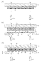
図1は本実施形態に係る半導体モジュールの概略断面図である。図1に基づいて本実施形態の半導体モジュールについて説明する。
図2および図3は突起部と溝部とを有する銅板の形成方法を説明するための概略断面図である。図4は複数のスクライブラインにより区画された半導体基板がマトリクス状に配置された半導体ウエハを示す平面図(上面図)である。図5および図6は図1に示した本実施形態に係る半導体モジュールの製造プロセスを説明するための概略断面図である。次に、図1〜図6を参照して本実施形態に係る半導体モジュールの製造プロセスについて説明する。
基板1の電極2aとの位置合わせ(重ね合わせ)を行い、半導体基板1(表面S側)と、突起部4aが形成された銅板4x(第1の主面S1側)との間に絶縁層8を挟持する。絶縁層8の厚さは、突起部4aの高さと同程度の約35μmである。なお、銅板4xと半導体基板1との位置合わせ方法については後述する。
導体ウエハ(半導体基板1)に絶縁層8を介して圧着する。この際、突起部4aが絶縁層8を貫通することにより突起部4aと半導体基板1の電極2aとが電気的に接続される。なお、位置合わせを行った後、別の装置にて圧着処理を行ってもよい。
上述の実施形態1では、銅板4zにおける半導体基板1の各電極2aに対応した位置に突起部4aを形成したが、本実施形態では銅板4xと半導体基板1のそれぞれの線膨張係数の差異と、銅板4xと半導体基板1の圧着時の加熱温度と、加熱にともなう膨張によって移動しない銅板4xの基準点からの距離とを考慮した位置に突起部4aを形成した点が実施形態1と異なる。以下、本実施形態について説明する。なお、実施形態1と同様の構成、方法については、同一の符号を付し、その説明は省略する。
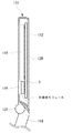
次に、本発明の各実施形態に係る半導体モジュールを備えた携帯機器について説明する。なお、携帯機器として携帯電話に搭載する例を示すが、たとえば、個人用携帯情報端末(PDA)、デジタルビデオカメラ(DVC)、及びデジタルスチルカメラ(DSC)といった電子機器であってもよい。
Claims (6)
- 表面に半導体素子と、この半導体素子と電気的に接続された電極と、所定の第1のパターン部とが設けられた基板を用意する第1の工程と、
第1の主面およびその反対側の第2の主面を有し、前記第1の主面から突出して設けられた突起部と前記第2の主面に設けられた所定パターンの溝部と当該溝部内に設けられた凸部とを備える金属板を用意する第2の工程と、
前記第1のパターン部とこれに対応する前記凸部とが所定の位置関係になるように金属板の位置を調整することで前記突起部と前記電極との位置合わせを行い、前記金属板の前記第1の主面側と前記基板とを絶縁層を介して圧着し、前記突起部が前記絶縁層を貫通した状態で前記突起部と前記電極とを電気的に接続する第3の工程と、
前記金属板の前記第2の主面側に所定パターンの配線層を形成する第4の工程と、
を備えることを特徴とする半導体モジュールの製造方法。 - 前記第4の工程は、前記金属板の前記第2の主面側をエッチバックして前記溝部の底部を前記第1の主面まで貫通させることにより前記金属板を所定パターンの配線層に加工していることを特徴とする請求項1に記載の半導体モジュールの製造方法。
- 前記第4の工程は、前記配線層の側面と、前記配線層の前記絶縁層と反対側の主面との間の領域が面取り形状となるように、前記金属板を加工していることを特徴とする請求項2に記載の半導体モジュールの製造方法。
- 前記第2の工程は、平板状の金属板の一方の面に前記突起部を形成する第1のステップと、前記突起部の所定の第2のパターン部を基準として前記平板状の金属板の他方の面に前記溝部および前記凸部を形成する第2のステップと、を備えていることを特徴とする請求項1に記載の半導体モジュールの製造方法。
- 前記半導体素子は前記基板に複数形成され、
前記溝部は複数の前記半導体素子間を区画するように設けられたスクライブ領域にさらに形成されていることを特徴とする請求項1に記載の半導体モジュールの製造方法。 - 前記第3の工程は、前記金属板の前記第1の主面側と前記基板とを加熱しながら圧着し、
前記第1のステップは、前記金属板の線膨張係数と前記基板の線膨張係数との差と、前記第3の工程における加熱温度と、前記第3の工程における加熱にともなう膨張によって移動しない前記金属板の基準点からの距離とに応じて、前記電極に対向する位置から前記金属板の膨張方向とは反対側にずらした位置に、前記突起部を形成していることを特徴とする請求項4に記載の半導体モジュールの製造方法。
Priority Applications (3)
| Application Number | Priority Date | Filing Date | Title |
|---|---|---|---|
| JP2008012240A JP4902558B2 (ja) | 2007-01-31 | 2008-01-23 | 半導体モジュールの製造方法 |
| US12/022,812 US7989359B2 (en) | 2007-01-31 | 2008-01-30 | Semiconductor module manufacturing method, semiconductor module, and mobile device |
| CN2008101277478A CN101303990B (zh) | 2007-01-31 | 2008-01-31 | 半导体模块的制造方法、半导体模块及便携设备 |
Applications Claiming Priority (3)
| Application Number | Priority Date | Filing Date | Title |
|---|---|---|---|
| JP2007020657 | 2007-01-31 | ||
| JP2007020657 | 2007-01-31 | ||
| JP2008012240A JP4902558B2 (ja) | 2007-01-31 | 2008-01-23 | 半導体モジュールの製造方法 |
Publications (3)
| Publication Number | Publication Date |
|---|---|
| JP2008211189A JP2008211189A (ja) | 2008-09-11 |
| JP2008211189A5 JP2008211189A5 (ja) | 2011-03-03 |
| JP4902558B2 true JP4902558B2 (ja) | 2012-03-21 |
Family
ID=39787193
Family Applications (1)
| Application Number | Title | Priority Date | Filing Date |
|---|---|---|---|
| JP2008012240A Expired - Fee Related JP4902558B2 (ja) | 2007-01-31 | 2008-01-23 | 半導体モジュールの製造方法 |
Country Status (3)
| Country | Link |
|---|---|
| US (1) | US7989359B2 (ja) |
| JP (1) | JP4902558B2 (ja) |
| CN (1) | CN101303990B (ja) |
Families Citing this family (10)
| Publication number | Priority date | Publication date | Assignee | Title |
|---|---|---|---|---|
| KR100823699B1 (ko) * | 2006-11-29 | 2008-04-21 | 삼성전자주식회사 | 플립칩 어셈블리 및 그 제조 방법 |
| JP2008211125A (ja) * | 2007-02-28 | 2008-09-11 | Spansion Llc | 半導体装置およびその製造方法 |
| JP4760930B2 (ja) * | 2009-02-27 | 2011-08-31 | 株式会社デンソー | Ic搭載基板、多層プリント配線板、及び製造方法 |
| JP2010262992A (ja) * | 2009-04-30 | 2010-11-18 | Sanyo Electric Co Ltd | 半導体モジュールおよび携帯機器 |
| TWI501376B (zh) * | 2009-10-07 | 2015-09-21 | Xintec Inc | 晶片封裝體及其製造方法 |
| US9484259B2 (en) | 2011-09-21 | 2016-11-01 | STATS ChipPAC Pte. Ltd. | Semiconductor device and method of forming protection and support structure for conductive interconnect structure |
| US9082832B2 (en) * | 2011-09-21 | 2015-07-14 | Stats Chippac, Ltd. | Semiconductor device and method of forming protection and support structure for conductive interconnect structure |
| US8664039B2 (en) * | 2011-10-18 | 2014-03-04 | Taiwan Semiconductor Manufacturing Company, Ltd. | Methods and apparatus for alignment in flip chip bonding |
| US9825209B2 (en) * | 2012-12-21 | 2017-11-21 | Panasonic Intellectual Property Management Co., Ltd. | Electronic component package and method for manufacturing the same |
| CN110164839B (zh) * | 2019-05-27 | 2020-01-31 | 广东工业大学 | 一种高密度线路嵌入转移的扇出型封装结构与方法 |
Family Cites Families (10)
| Publication number | Priority date | Publication date | Assignee | Title |
|---|---|---|---|---|
| US5821627A (en) * | 1993-03-11 | 1998-10-13 | Kabushiki Kaisha Toshiba | Electronic circuit device |
| JP3533284B2 (ja) | 1996-04-24 | 2004-05-31 | 新光電気工業株式会社 | 半導体装置用基板及びその製造方法並びに半導体装置 |
| JP3968788B2 (ja) * | 1997-03-21 | 2007-08-29 | セイコーエプソン株式会社 | 半導体装置及びフィルムキャリアテープの製造方法 |
| JP2000068641A (ja) | 1998-08-20 | 2000-03-03 | Mitsubishi Gas Chem Co Inc | プリント配線板の製造方法 |
| MY144574A (en) * | 1998-09-14 | 2011-10-14 | Ibiden Co Ltd | Printed circuit board and method for its production |
| JP2001053195A (ja) * | 1999-08-11 | 2001-02-23 | Mitsui High Tec Inc | 半導体装置の製造方法 |
| JP2001223287A (ja) * | 2000-02-07 | 2001-08-17 | Mitsui High Tec Inc | インターポーザーの製造方法 |
| JP3767398B2 (ja) * | 2001-03-19 | 2006-04-19 | カシオ計算機株式会社 | 半導体装置およびその製造方法 |
| JP2006310530A (ja) * | 2005-04-28 | 2006-11-09 | Sanyo Electric Co Ltd | 回路装置およびその製造方法 |
| JP4568215B2 (ja) * | 2005-11-30 | 2010-10-27 | 三洋電機株式会社 | 回路装置および回路装置の製造方法 |
-
2008
- 2008-01-23 JP JP2008012240A patent/JP4902558B2/ja not_active Expired - Fee Related
- 2008-01-30 US US12/022,812 patent/US7989359B2/en not_active Expired - Fee Related
- 2008-01-31 CN CN2008101277478A patent/CN101303990B/zh not_active Expired - Fee Related
Also Published As
| Publication number | Publication date |
|---|---|
| CN101303990B (zh) | 2011-08-24 |
| CN101303990A (zh) | 2008-11-12 |
| US20080284012A1 (en) | 2008-11-20 |
| US7989359B2 (en) | 2011-08-02 |
| JP2008211189A (ja) | 2008-09-11 |
Similar Documents
| Publication | Publication Date | Title |
|---|---|---|
| JP4902558B2 (ja) | 半導体モジュールの製造方法 | |
| JP5091600B2 (ja) | 半導体モジュール、半導体モジュールの製造方法および携帯機器 | |
| WO2010067610A1 (ja) | 半導体モジュール、半導体モジュールの製造方法および携帯機器 | |
| JP5135246B2 (ja) | 半導体モジュールおよびその製造方法、ならびに携帯機器 | |
| JP2010087229A (ja) | 半導体モジュール、半導体モジュールの製造方法および携帯機器 | |
| JP5064158B2 (ja) | 半導体装置とその製造方法 | |
| JP2008053693A (ja) | 半導体モジュール、携帯機器、および半導体モジュールの製造方法 | |
| JP4588091B2 (ja) | 半導体モジュールの製造方法 | |
| JP2009224581A (ja) | 素子搭載用基板およびその製造方法、半導体モジュールおよびその製造方法、電極構造、携帯機器 | |
| US8362611B2 (en) | Semiconductor module, method for manufacturing semiconductor module, and portable device | |
| JP2009158830A (ja) | 素子搭載用基板およびその製造方法、半導体モジュールおよびその製造方法、ならびに携帯機器 | |
| US20100140797A1 (en) | Device mounting board and method of manufacturing the board, semiconductor module and method of manufacturing the module | |
| JP5295211B2 (ja) | 半導体モジュールの製造方法 | |
| JP2010040721A (ja) | 半導体モジュール、半導体装置、携帯機器、半導体モジュールの製造方法および半導体装置の製造方法 | |
| JP4806468B2 (ja) | 半導体モジュール | |
| JP5061010B2 (ja) | 半導体モジュール | |
| JP2009027042A (ja) | 回路モジュール、回路モジュールの製造方法および携帯機器 | |
| JP5002633B2 (ja) | 半導体モジュールおよび携帯機器 | |
| JP2009158751A (ja) | 素子搭載用基板およびその製造方法、半導体モジュールおよびその製造方法、ならびに携帯機器 | |
| JP2009212114A (ja) | 突起電極の構造、素子搭載用基板およびその製造方法、半導体モジュール、ならびに携帯機器 | |
| JP5140565B2 (ja) | 素子搭載用基板、半導体モジュール、および携帯機器 | |
| JP2011082447A (ja) | 素子搭載用基板、半導体モジュールおよび携帯機器 | |
| JP2009238900A (ja) | 突起電極の構造、素子搭載用基板およびその製造方法、半導体モジュール、ならびに携帯機器 | |
| US20100248429A1 (en) | Method for manufacturing semiconductor modules | |
| JP2010087034A (ja) | 半導体モジュールおよび半導体モジュールの製造方法、および携帯機器 |
Legal Events
| Date | Code | Title | Description |
|---|---|---|---|
| A521 | Written amendment |
Free format text: JAPANESE INTERMEDIATE CODE: A523 Effective date: 20110119 |
|
| A621 | Written request for application examination |
Free format text: JAPANESE INTERMEDIATE CODE: A621 Effective date: 20110119 |
|
| A977 | Report on retrieval |
Free format text: JAPANESE INTERMEDIATE CODE: A971007 Effective date: 20110926 |
|
| A131 | Notification of reasons for refusal |
Free format text: JAPANESE INTERMEDIATE CODE: A131 Effective date: 20111004 |
|
| A521 | Written amendment |
Free format text: JAPANESE INTERMEDIATE CODE: A523 Effective date: 20111116 |
|
| TRDD | Decision of grant or rejection written | ||
| A01 | Written decision to grant a patent or to grant a registration (utility model) |
Free format text: JAPANESE INTERMEDIATE CODE: A01 Effective date: 20111206 |
|
| A01 | Written decision to grant a patent or to grant a registration (utility model) |
Free format text: JAPANESE INTERMEDIATE CODE: A01 |
|
| A61 | First payment of annual fees (during grant procedure) |
Free format text: JAPANESE INTERMEDIATE CODE: A61 Effective date: 20111228 |
|
| R151 | Written notification of patent or utility model registration |
Ref document number: 4902558 Country of ref document: JP Free format text: JAPANESE INTERMEDIATE CODE: R151 |
|
| FPAY | Renewal fee payment (event date is renewal date of database) |
Free format text: PAYMENT UNTIL: 20150113 Year of fee payment: 3 |
|
| LAPS | Cancellation because of no payment of annual fees |