JP4640802B2 - 回路付サスペンション基板 - Google Patents
回路付サスペンション基板 Download PDFInfo
- Publication number
- JP4640802B2 JP4640802B2 JP2005199035A JP2005199035A JP4640802B2 JP 4640802 B2 JP4640802 B2 JP 4640802B2 JP 2005199035 A JP2005199035 A JP 2005199035A JP 2005199035 A JP2005199035 A JP 2005199035A JP 4640802 B2 JP4640802 B2 JP 4640802B2
- Authority
- JP
- Japan
- Prior art keywords
- metal
- metal foil
- opening
- insulating layer
- thin film
- Prior art date
- Legal status (The legal status is an assumption and is not a legal conclusion. Google has not performed a legal analysis and makes no representation as to the accuracy of the status listed.)
- Expired - Fee Related
Links
Images


Classifications
-
- H—ELECTRICITY
- H05—ELECTRIC TECHNIQUES NOT OTHERWISE PROVIDED FOR
- H05K—PRINTED CIRCUITS; CASINGS OR CONSTRUCTIONAL DETAILS OF ELECTRIC APPARATUS; MANUFACTURE OF ASSEMBLAGES OF ELECTRICAL COMPONENTS
- H05K3/00—Apparatus or processes for manufacturing printed circuits
- H05K3/38—Improvement of the adhesion between the insulating substrate and the metal
-
- H—ELECTRICITY
- H05—ELECTRIC TECHNIQUES NOT OTHERWISE PROVIDED FOR
- H05K—PRINTED CIRCUITS; CASINGS OR CONSTRUCTIONAL DETAILS OF ELECTRIC APPARATUS; MANUFACTURE OF ASSEMBLAGES OF ELECTRICAL COMPONENTS
- H05K3/00—Apparatus or processes for manufacturing printed circuits
- H05K3/44—Manufacturing insulated metal core circuits or other insulated electrically conductive core circuits
-
- H—ELECTRICITY
- H05—ELECTRIC TECHNIQUES NOT OTHERWISE PROVIDED FOR
- H05K—PRINTED CIRCUITS; CASINGS OR CONSTRUCTIONAL DETAILS OF ELECTRIC APPARATUS; MANUFACTURE OF ASSEMBLAGES OF ELECTRICAL COMPONENTS
- H05K1/00—Printed circuits
- H05K1/02—Details
- H05K1/03—Use of materials for the substrate
- H05K1/05—Insulated conductive substrates, e.g. insulated metal substrate
- H05K1/056—Insulated conductive substrates, e.g. insulated metal substrate the metal substrate being covered by an organic insulating layer
-
- H—ELECTRICITY
- H05—ELECTRIC TECHNIQUES NOT OTHERWISE PROVIDED FOR
- H05K—PRINTED CIRCUITS; CASINGS OR CONSTRUCTIONAL DETAILS OF ELECTRIC APPARATUS; MANUFACTURE OF ASSEMBLAGES OF ELECTRICAL COMPONENTS
- H05K2201/00—Indexing scheme relating to printed circuits covered by H05K1/00
- H05K2201/03—Conductive materials
- H05K2201/0332—Structure of the conductor
- H05K2201/0364—Conductor shape
- H05K2201/0379—Stacked conductors
-
- H—ELECTRICITY
- H05—ELECTRIC TECHNIQUES NOT OTHERWISE PROVIDED FOR
- H05K—PRINTED CIRCUITS; CASINGS OR CONSTRUCTIONAL DETAILS OF ELECTRIC APPARATUS; MANUFACTURE OF ASSEMBLAGES OF ELECTRICAL COMPONENTS
- H05K2201/00—Indexing scheme relating to printed circuits covered by H05K1/00
- H05K2201/09—Shape and layout
- H05K2201/09209—Shape and layout details of conductors
- H05K2201/09654—Shape and layout details of conductors covering at least two types of conductors provided for in H05K2201/09218 - H05K2201/095
- H05K2201/0969—Apertured conductors
-
- H—ELECTRICITY
- H05—ELECTRIC TECHNIQUES NOT OTHERWISE PROVIDED FOR
- H05K—PRINTED CIRCUITS; CASINGS OR CONSTRUCTIONAL DETAILS OF ELECTRIC APPARATUS; MANUFACTURE OF ASSEMBLAGES OF ELECTRICAL COMPONENTS
- H05K2201/00—Indexing scheme relating to printed circuits covered by H05K1/00
- H05K2201/09—Shape and layout
- H05K2201/09209—Shape and layout details of conductors
- H05K2201/09654—Shape and layout details of conductors covering at least two types of conductors provided for in H05K2201/09218 - H05K2201/095
- H05K2201/09781—Dummy conductors, i.e. not used for normal transport of current; Dummy electrodes of components
-
- H—ELECTRICITY
- H05—ELECTRIC TECHNIQUES NOT OTHERWISE PROVIDED FOR
- H05K—PRINTED CIRCUITS; CASINGS OR CONSTRUCTIONAL DETAILS OF ELECTRIC APPARATUS; MANUFACTURE OF ASSEMBLAGES OF ELECTRICAL COMPONENTS
- H05K2201/00—Indexing scheme relating to printed circuits covered by H05K1/00
- H05K2201/20—Details of printed circuits not provided for in H05K2201/01 - H05K2201/10
- H05K2201/2072—Anchoring, i.e. one structure gripping into another
-
- H—ELECTRICITY
- H05—ELECTRIC TECHNIQUES NOT OTHERWISE PROVIDED FOR
- H05K—PRINTED CIRCUITS; CASINGS OR CONSTRUCTIONAL DETAILS OF ELECTRIC APPARATUS; MANUFACTURE OF ASSEMBLAGES OF ELECTRICAL COMPONENTS
- H05K2203/00—Indexing scheme relating to apparatus or processes for manufacturing printed circuits covered by H05K3/00
- H05K2203/03—Metal processing
- H05K2203/0323—Working metal substrate or core, e.g. by etching, deforming
-
- H—ELECTRICITY
- H05—ELECTRIC TECHNIQUES NOT OTHERWISE PROVIDED FOR
- H05K—PRINTED CIRCUITS; CASINGS OR CONSTRUCTIONAL DETAILS OF ELECTRIC APPARATUS; MANUFACTURE OF ASSEMBLAGES OF ELECTRICAL COMPONENTS
- H05K3/00—Apparatus or processes for manufacturing printed circuits
- H05K3/02—Apparatus or processes for manufacturing printed circuits in which the conductive material is applied to the surface of the insulating support and is thereafter removed from such areas of the surface which are not intended for current conducting or shielding
- H05K3/06—Apparatus or processes for manufacturing printed circuits in which the conductive material is applied to the surface of the insulating support and is thereafter removed from such areas of the surface which are not intended for current conducting or shielding the conductive material being removed chemically or electrolytically, e.g. by photo-etch process
-
- H—ELECTRICITY
- H05—ELECTRIC TECHNIQUES NOT OTHERWISE PROVIDED FOR
- H05K—PRINTED CIRCUITS; CASINGS OR CONSTRUCTIONAL DETAILS OF ELECTRIC APPARATUS; MANUFACTURE OF ASSEMBLAGES OF ELECTRICAL COMPONENTS
- H05K3/00—Apparatus or processes for manufacturing printed circuits
- H05K3/10—Apparatus or processes for manufacturing printed circuits in which conductive material is applied to the insulating support in such a manner as to form the desired conductive pattern
- H05K3/20—Apparatus or processes for manufacturing printed circuits in which conductive material is applied to the insulating support in such a manner as to form the desired conductive pattern by affixing prefabricated conductor pattern
- H05K3/205—Apparatus or processes for manufacturing printed circuits in which conductive material is applied to the insulating support in such a manner as to form the desired conductive pattern by affixing prefabricated conductor pattern using a pattern electroplated or electroformed on a metallic carrier
Landscapes
- Engineering & Computer Science (AREA)
- Manufacturing & Machinery (AREA)
- Microelectronics & Electronic Packaging (AREA)
- Insulated Metal Substrates For Printed Circuits (AREA)
- Adjustment Of The Magnetic Head Position Track Following On Tapes (AREA)
- Supporting Of Heads In Record-Carrier Devices (AREA)
- Structure Of Printed Boards (AREA)
Description
本発明の回路付サスペンション基板によれば、金属箔は、開口部内に配置される第1金属箔部分と、金属支持基板における開口部の端縁と絶縁層との接触部分を挟むように、第1金属箔部分と間隔を隔てて配置され、金属支持基板と対向する第2金属箔部分とを備えている。そのため、金属支持基板における開口部の端縁の密着性を向上させながら、金属箔の設置面積を十分に確保することができる。その結果、簡易な構成により、導体パターンの伝送損失の低減をより一層図ることができる。
本発明の回路付サスペンション基板によれば、簡易な層構成により、金属支持基板と第2金属箔部分との密着性を向上させることができる。そのため、金属支持基板の剥離をより一層有効に防止することができる。
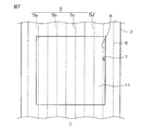
図1において、この回路付サスペンション基板1は、ハードディスクドライブに搭載される回路付サスペンション基板であって、金属支持基板2と、金属支持基板2の上に形成される絶縁層としてのベース絶縁層3と、ベース絶縁層3の上に形成される導体パターン5と、ベース絶縁層3内に埋設される金属箔6とを備えている。また、この回路付サスペンション基板1には、導体パターン5を被覆するように、ベース絶縁層3の上にカバー絶縁層4が形成されている。
第1金属箔部分9は、図2に示すように、第2金属箔部分10と隙間S1を隔てて、第2金属箔部分10内に形成されている。この第1金属箔部分9は、導体パターン5の長手方向途中と対向するように設けられ、後述する開口部7よりもやや小さな底面視矩形状に形成されている。
より具体的には、この第1金属箔部分9は、その幅が、例えば、0.05〜10mm、好ましくは、0.1〜2mmで形成され、その長さが、例えば、0.05〜10mm、好ましくは、0.1〜2mmで形成されている。
この第2金属箔部分10は、その幅が、配線5aおよび5dの外側端縁の間の長さよりも幅広く、かつ、金属支持基板2よりも幅狭い長さで形成され、その長さが、第1金属箔部分9よりも長い所望の長さで、形成されている。
また、金属箔6の下面には、図1に示すように、金属薄膜11が形成されている。
そして、この回路付サスペンション基板1には、金属支持基板2に、開口部7が形成されている。
まず、図3(a)に示すように、金属支持基板2を用意し、その金属支持基板2の表面全面に、スパッタリングまたは電解めっきにより、金属薄膜11を形成する。
次に、図3(b)に示すように、めっきレジスト16を上記した金属箔6の反転パターンで形成する。めっきレジスト16の形成は、例えば、ドライフィルムレジストを用いて露光および現像する、公知の方法が用いられる。
次に、図3(d)に示すように、めっきレジスト16およびめっきレジスト16が形成されていた部分の金属薄膜11を、例えば、化学エッチング(ウェットエッチング)などの公知のエッチング法または剥離によって除去する。
次に、図3(f)に示すように、金属箔6、金属薄膜11および保護薄膜17を被覆するように、金属支持基板2の上に、例えば、上記した合成樹脂の溶液(ワニス)を均一に塗布した後、乾燥し、次いで、必要に応じて、加熱することによって硬化させ、ベース絶縁層3を形成する。なお、ベース絶縁層3は、感光性の合成樹脂を露光および現像することにより、パターンとして、形成することもできる。さらに、ベース絶縁層3の形成は、上記の方法に特に制限されず、例えば、予め合成樹脂をフィルムに形成して、そのフィルムを、金属箔6、金属薄膜11および保護薄膜17を被覆するように、金属支持基板2の上に、公知の接着剤層を介して貼着することもできる。
例えば、アディティブ法により、導体パターン5を形成する場合には、まず、ベース絶縁層3の表面全面に、例えば、真空成膜法やスパッタリング法などにより、下地となる導体薄膜を形成し、その導体薄膜の表面に、ドライフィルムレジストなどを用いて露光および現像し、導体パターン5の反転パターンでめっきレジストを形成する。次いで、めっきにより、めっきレジストから露出する導体薄膜の表面に、導体パターン5を形成し、めっきレジストおよびめっきレジストが形成されていた部分の導体薄膜をエッチングまたは剥離などにより除去する。なお、めっきは、電解めっき、無電解めっきのいずれでもよいが、電解めっきが好ましく用いられ、電解銅めっきがさらに好ましく用いられる。
このようにして得られる回路付サスペンション基板1では、図1および図2に示すように、第1金属箔部分9が、開口部7内に配置され、開口部7の開口端縁8と重ならないように、ベース絶縁層3から露出されており、金属支持基板2における開口部7の開口端縁8が、ベース絶縁層3に直接接触している。そのため、金属支持基板2における開口部7の開口端縁8の密着性を向上させることができる。その結果、簡易な構成により、導体パターン5の特性インピーダンスの調整や伝送損失の低減を図りつつ、金属支持基板2の剥離を有効に防止することができる。
なお、上記した回路付サスペンション基板1では、金属箔6を、第1金属箔部分9と第2金属箔部分10とを備えるパターンとして形成したが、図4および図5に示すように、金属箔6を、第2金属箔部分10を備えずに、第1金属箔部分9のみからなるパターンとして形成してもよい。金属箔6を第1金属箔部分9のみから形成しても、金属支持基板2における開口部7の開口端縁8を、ベース絶縁層3に直接接触させることができる。そのため、金属支持基板2における開口部7の開口端縁8の密着性を向上させることができる。その結果、簡易な構成により、導体パターン5の特性インピーダンスの調整や伝送損失の低減を図りつつ、金属支持基板2の剥離を有効に防止することができる。
また、上記の説明においては、開口部7を底面視矩形状に形成したが、開口部7の形状は特に制限されず、底面視円形状などであってもよい。
実施例1
金属支持基板として、厚み25μmのステンレス基板の上に、金属薄膜として、厚み0.03μmのクロム薄膜と厚み0.07μmの銅薄膜とをスパッタリングによって順次形成した(図3(a)参照)。次いで、金属箔の反転パターンでめっきレジストを、ドライフィルムレジストを用いて形成した(図3(b)参照)。次いで、めっきレジストから露出する金属薄膜の表面に、金属箔として、厚み4.0μmの銅箔を、硫酸銅水溶液を用いて電解銅めっきにより形成した(図3(c)参照)。なお、この銅箔は、第1金属箔部分としての第1銅箔部分と、第2金属箔部分としての第2銅箔部分とを備えるパターンとして形成した(図2参照)。次いで、めっきレジストを、水酸化ナトリウム水溶液を用いて剥離により除去した後、めっきレジストが形成されていた部分の金属薄膜をエッチングにより除去し(図3(d)参照)、金属箔および金属薄膜の表面(金属箔の上面および側面と、金属薄膜の側面との各面)に、保護薄膜として、厚み0.1μmのニッケル薄膜を無電解めっきにより形成した(図3(e)参照)。次いで、金属箔、金属薄膜、および、保護薄膜を被覆するように、金属支持基板の上に、感光性ポリアミック酸樹脂のワニスを塗布後、露光および現像し、さらに加熱硬化することにより、厚み10μmのポリイミドからなるベース絶縁層を形成した(図3(f)参照)。次いで、そのベース絶縁層の表面に、アディティブ法によって、厚み10μmの導体パターンを形成した(図3(g)参照)。次いで、導体パターンを被覆するように、ベース絶縁層の上に、感光性ポリアミック酸樹脂のワニスを塗布後、露光および現像し、さらに加熱硬化することにより、厚み5μmのポリイミドからなるカバー絶縁層を形成した(図3(h)参照)。次いで、ステンレス基板に、エッチングにより、開口部を底面視矩形状に形成した(図3(i)、図1、図2参照)。その後、金属支持基板をエッチングにより切り抜き、回路付サスペンション基板を得た。
得られた回路付サスペンション基板を、開口部で折り曲げても、回路付サスペンション基板は、その開口部において、金属支持基板がベース絶縁層から剥離しなかった。
実施例1において、金属箔を、第1金属箔部分と第2金属箔部分との間に隙間S1を設けることなく第1金属箔部分と第2金属箔部分とが連続するように形成し、かつ、金属支持基板における開口部を、その開口端縁がベース絶縁層に接触せず、金属箔と重なるように形成した以外は、実施例1と同様にして、回路付サスペンション基板を得た(図6および図7参照)。
得られた回路付サスペンション基板を、開口部で折り曲げたところ、回路付サスペンション基板は、その開口部において、金属支持基板がベース絶縁層から剥離した。
2 金属支持基板
3 ベース絶縁層
5 導体パターン
6 金属箔
7 開口部
8 開口端縁
9 第1金属箔部分
10 第2金属箔部分
11 金属薄膜
Claims (4)
- 金属支持基板と、前記金属支持基板の上に形成される絶縁層と、前記絶縁層の上に形成され、4つの配線を有する導体パターンと、前記絶縁層内に埋設される金属箔とを備え、
前記金属支持基板には、前記導体パターンと対向する開口部が形成されており、
前記金属箔は、少なくとも一部が、前記開口部内に前記導体パターンと対向するように配置されており、前記開口部の端縁と重ならないように、前記絶縁層から露出されており、
前記金属支持基板における前記開口部の端縁の少なくとも一部が、前記絶縁層に直接接触していることを特徴とする、回路付サスペンション基板。 - 前記金属箔は、
前記開口部内に配置される第1金属箔部分と、
前記金属支持基板における前記開口部の端縁と前記絶縁層との接触部分を挟むように、前記第1金属箔部分と間隔を隔てて配置され、前記金属支持基板と対向する第2金属箔部分とを備えていることを特徴とする、請求項1に記載の回路付サスペンション基板。 - 前記金属支持基板と前記第2金属箔部分との間には、金属薄膜が介在されていることを特徴とする、請求項2に記載の回路付サスペンション基板。
- 前記金属支持基板が、ステンレスからなり、
前記金属箔が、銅または銅合金からなり、
前記絶縁層が、ポリイミドからなることを特徴とする、請求項1〜3のいずれかに記載の回路付サスペンション基板。
Priority Applications (3)
| Application Number | Priority Date | Filing Date | Title |
|---|---|---|---|
| JP2005199035A JP4640802B2 (ja) | 2005-07-07 | 2005-07-07 | 回路付サスペンション基板 |
| US11/477,935 US8134080B2 (en) | 2005-07-07 | 2006-06-30 | Wired circuit board |
| CN200610101338A CN100586251C (zh) | 2005-07-07 | 2006-07-07 | 布线电路板 |
Applications Claiming Priority (1)
| Application Number | Priority Date | Filing Date | Title |
|---|---|---|---|
| JP2005199035A JP4640802B2 (ja) | 2005-07-07 | 2005-07-07 | 回路付サスペンション基板 |
Publications (2)
| Publication Number | Publication Date |
|---|---|
| JP2007019261A JP2007019261A (ja) | 2007-01-25 |
| JP4640802B2 true JP4640802B2 (ja) | 2011-03-02 |
Family
ID=37598146
Family Applications (1)
| Application Number | Title | Priority Date | Filing Date |
|---|---|---|---|
| JP2005199035A Expired - Fee Related JP4640802B2 (ja) | 2005-07-07 | 2005-07-07 | 回路付サスペンション基板 |
Country Status (3)
| Country | Link |
|---|---|
| US (1) | US8134080B2 (ja) |
| JP (1) | JP4640802B2 (ja) |
| CN (1) | CN100586251C (ja) |
Families Citing this family (19)
| Publication number | Priority date | Publication date | Assignee | Title |
|---|---|---|---|---|
| JP4640802B2 (ja) | 2005-07-07 | 2011-03-02 | 日東電工株式会社 | 回路付サスペンション基板 |
| JP4865453B2 (ja) | 2006-08-30 | 2012-02-01 | 日東電工株式会社 | 配線回路基板およびその製造方法 |
| JP2008282995A (ja) | 2007-05-10 | 2008-11-20 | Nitto Denko Corp | 配線回路基板 |
| JP2009016610A (ja) * | 2007-07-05 | 2009-01-22 | Nitto Denko Corp | 配線回路基板およびその製造方法 |
| JP4992648B2 (ja) * | 2007-10-05 | 2012-08-08 | 大日本印刷株式会社 | サスペンション基板およびその製造方法 |
| JP6021211B2 (ja) * | 2010-04-30 | 2016-11-09 | 大日本印刷株式会社 | サスペンション用基板、サスペンション、素子付サスペンションおよびハードディスクドライブ |
| JP5861274B2 (ja) * | 2011-05-24 | 2016-02-16 | 大日本印刷株式会社 | サスペンション用フレキシャー基板、サスペンション、ヘッド付サスペンション、およびハードディスクドライブ |
| JP5349634B2 (ja) * | 2012-03-16 | 2013-11-20 | 日東電工株式会社 | 回路付サスペンション基板 |
| JP6025384B2 (ja) * | 2012-04-27 | 2016-11-16 | 日東電工株式会社 | 配線回路基板およびその製造方法 |
| CN103889152A (zh) * | 2012-12-20 | 2014-06-25 | 深南电路有限公司 | 印刷电路板加工方法 |
| USD784936S1 (en) * | 2014-05-28 | 2017-04-25 | Sumitomo Electric Industries, Ltd. | Flexible printed wiring board with device |
| USD785575S1 (en) * | 2014-05-28 | 2017-05-02 | Sumitomo Electric Industries, Ltd. | Flexible printed wiring board |
| JP6484073B2 (ja) * | 2015-03-10 | 2019-03-13 | 日東電工株式会社 | 回路付サスペンション基板 |
| JP6128184B2 (ja) * | 2015-10-30 | 2017-05-17 | 大日本印刷株式会社 | サスペンション用フレキシャー基板、サスペンション、ヘッド付サスペンション、およびハードディスクドライブ |
| JP6808266B2 (ja) * | 2016-05-18 | 2021-01-06 | 日東電工株式会社 | 配線回路基板およびその製造方法 |
| US9905519B1 (en) * | 2016-08-29 | 2018-02-27 | Via Alliance Semiconductor Co., Ltd. | Electronic structure process |
| US10002839B2 (en) * | 2016-08-29 | 2018-06-19 | Via Alliance Semiconductor Co., Ltd. | Electronic structure, and electronic structure array |
| JP6909566B2 (ja) * | 2016-09-06 | 2021-07-28 | 日東電工株式会社 | 配線回路基板およびその製造方法 |
| JP2024008277A (ja) * | 2022-07-07 | 2024-01-19 | 日東電工株式会社 | 配線回路基板およびその製造方法 |
Family Cites Families (62)
| Publication number | Priority date | Publication date | Assignee | Title |
|---|---|---|---|---|
| JPS59219492A (ja) | 1983-05-27 | 1984-12-10 | Nisshin Steel Co Ltd | 片面銅めつきステンレス鋼板の製造法 |
| JPH0728130B2 (ja) | 1987-12-07 | 1995-03-29 | 株式会社ミツトヨ | 立体パターン配線構造およびその製造方法 |
| JPH03274799A (ja) | 1990-03-23 | 1991-12-05 | Fuji Electric Co Ltd | 半導体装置の金属絶縁基板 |
| JPH05304345A (ja) | 1992-04-27 | 1993-11-16 | Sanken Electric Co Ltd | 金属製配線基板及びその製造方法 |
| US5612512A (en) * | 1992-11-11 | 1997-03-18 | Murata Manufacturing Co., Ltd. | High frequency electronic component having base substrate formed of bismaleimide-triazine resin and resistant film formed on base substrate |
| JP3461204B2 (ja) * | 1993-09-14 | 2003-10-27 | 株式会社東芝 | マルチチップモジュール |
| JPH07202365A (ja) | 1993-12-28 | 1995-08-04 | Fujitsu Ltd | 半導体実装基板 |
| US6162996A (en) * | 1994-03-23 | 2000-12-19 | Dyconex Patente Ag | Insulating foil circuit board with rigid and flexible sections |
| TW289900B (ja) * | 1994-04-22 | 1996-11-01 | Gould Electronics Inc | |
| JP3354302B2 (ja) * | 1994-07-27 | 2002-12-09 | 日本メクトロン株式会社 | 磁気ヘッド用サスペンションの製造法 |
| JPH08241894A (ja) | 1995-03-03 | 1996-09-17 | Fujitsu Ltd | レーザ・アブレーション加工方法 |
| JPH08307020A (ja) | 1995-05-08 | 1996-11-22 | Nitto Denko Corp | 回路形成用基板および回路基板 |
| US5608591A (en) * | 1995-06-09 | 1997-03-04 | International Business Machines Corporation | Integrated head-electronics interconnection suspension for a data recording disk drive |
| JP3274799B2 (ja) | 1995-11-30 | 2002-04-15 | キヤノン株式会社 | 加圧回転体及び定着装置並びに画像記録装置 |
| US5776824A (en) * | 1995-12-22 | 1998-07-07 | Micron Technology, Inc. | Method for producing laminated film/metal structures for known good die ("KG") applications |
| CN1106788C (zh) * | 1996-02-13 | 2003-04-23 | 日东电工株式会社 | 电路基片 |
| JP3206428B2 (ja) * | 1996-04-09 | 2001-09-10 | ティーディーケイ株式会社 | ヘッドジンバルアセンブリを具備するハードディスク装置 |
| JPH10261212A (ja) | 1996-09-27 | 1998-09-29 | Nippon Mektron Ltd | 回路配線付き磁気ヘッド用サスペンションの製造法 |
| US5796552A (en) | 1996-10-03 | 1998-08-18 | Quantum Corporation | Suspension with biaxially shielded conductor trace array |
| KR19980041830A (ko) | 1996-11-19 | 1998-08-17 | 포만제프리엘 | 제어된 붕괴형 칩 접속을 위한 박막 야금물 및 구조물 |
| US5812344A (en) * | 1997-05-12 | 1998-09-22 | Quantum Corporation | Suspension with integrated conductor trace array having optimized cross-sectional high frequency current density |
| US5862010A (en) * | 1997-07-08 | 1999-01-19 | International Business Machines Corporation | Transducer suspension system |
| JP3862454B2 (ja) | 1999-09-16 | 2006-12-27 | 電気化学工業株式会社 | 金属ベース多層回路基板 |
| JP4356215B2 (ja) * | 1999-11-10 | 2009-11-04 | 凸版印刷株式会社 | フレクシャ及びその製造方法ならびにそれに用いるフレクシャ用基板 |
| EP1100295B1 (en) * | 1999-11-12 | 2012-03-28 | Panasonic Corporation | Capacitor-mounted metal foil and a method for producing the same, and a circuit board and a method for producing the same |
| JP2001209918A (ja) * | 1999-11-19 | 2001-08-03 | Nitto Denko Corp | 回路付サスペンション基板 |
| US6480359B1 (en) | 2000-05-09 | 2002-11-12 | 3M Innovative Properties Company | Hard disk drive suspension with integral flexible circuit |
| JP3935309B2 (ja) * | 2000-06-08 | 2007-06-20 | 日東電工株式会社 | 配線回路基板およびその製造方法 |
| JP2002111205A (ja) | 2000-07-27 | 2002-04-12 | Sumitomo Bakelite Co Ltd | 多層配線板の製造方法および多層配線板 |
| JP3751805B2 (ja) | 2000-08-11 | 2006-03-01 | 日東電工株式会社 | 金属薄膜の形成方法 |
| KR100379128B1 (ko) * | 2000-08-23 | 2003-04-08 | 주식회사 아큐텍반도체기술 | 삼원합금을 이용한 환경친화적 반도체 장치 제조용 기질 |
| JP4447762B2 (ja) | 2000-10-18 | 2010-04-07 | 東洋鋼鈑株式会社 | 多層金属積層板及びその製造方法 |
| JP4448610B2 (ja) * | 2000-10-18 | 2010-04-14 | 日東電工株式会社 | 回路基板の製造方法 |
| JP3546961B2 (ja) | 2000-10-18 | 2004-07-28 | 日本電気株式会社 | 半導体装置搭載用配線基板およびその製造方法、並びに半導体パッケージ |
| JP2002222578A (ja) * | 2001-01-26 | 2002-08-09 | Nitto Denko Corp | 中継フレキシブル配線回路基板 |
| JP3654198B2 (ja) | 2001-02-23 | 2005-06-02 | Tdk株式会社 | ヘッドジンバルアセンブリ |
| JP3895125B2 (ja) * | 2001-04-12 | 2007-03-22 | 日東電工株式会社 | 補強板付フレキシブルプリント回路板 |
| US6861757B2 (en) * | 2001-09-03 | 2005-03-01 | Nec Corporation | Interconnecting substrate for carrying semiconductor device, method of producing thereof and package of semiconductor device |
| CN1415474A (zh) | 2001-10-29 | 2003-05-07 | 造利科技股份有限公司 | 具有载体的转印背胶式铜箔制造方法 |
| JP3921379B2 (ja) | 2001-11-09 | 2007-05-30 | 株式会社日立グローバルストレージテクノロジーズ | ヘッド支持機構体及び磁気ディスク装置 |
| JP3931074B2 (ja) | 2001-11-09 | 2007-06-13 | 株式会社日立グローバルストレージテクノロジーズ | 信号伝送線路及びそれを備えたサスペンション並びに記録装置 |
| JP2003197459A (ja) | 2001-12-26 | 2003-07-11 | Kyocera Corp | 積層型電子部品の製法 |
| JP2004014975A (ja) | 2002-06-11 | 2004-01-15 | Nitto Denko Corp | 金属箔付フレキシブル回路基板 |
| JP2004088020A (ja) | 2002-08-29 | 2004-03-18 | Toshiba Corp | フレキシブルプリント基板及び該基板を備えた電子機器 |
| JP2004111578A (ja) | 2002-09-17 | 2004-04-08 | Dainippon Printing Co Ltd | ヒートスプレッダー付きビルドアップ型の配線基板の製造方法とヒートスプレッダー付きビルドアップ型の配線基板 |
| JP2004186342A (ja) | 2002-12-02 | 2004-07-02 | Kyocera Corp | セラミック積層体及びその製法 |
| KR100584965B1 (ko) * | 2003-02-24 | 2006-05-29 | 삼성전기주식회사 | 패키지 기판 및 그 제조 방법 |
| JP4222882B2 (ja) * | 2003-06-03 | 2009-02-12 | 日東電工株式会社 | 配線回路基板 |
| JP4178077B2 (ja) * | 2003-06-04 | 2008-11-12 | 日東電工株式会社 | 配線回路基板 |
| JP4222885B2 (ja) | 2003-06-04 | 2009-02-12 | 日東電工株式会社 | 配線回路基板 |
| JP2005011387A (ja) * | 2003-06-16 | 2005-01-13 | Hitachi Global Storage Technologies Inc | 磁気ディスク装置 |
| JP4019034B2 (ja) * | 2003-09-22 | 2007-12-05 | 日東電工株式会社 | 回路付サスペンション基板の製造方法 |
| JP2005158973A (ja) | 2003-11-25 | 2005-06-16 | Matsushita Electric Works Ltd | 多層回路基板及び多層回路基板の製造方法 |
| JP4028477B2 (ja) * | 2003-12-04 | 2007-12-26 | 日東電工株式会社 | 回路付サスペンション基板およびその製造方法 |
| JP2005235318A (ja) | 2004-02-20 | 2005-09-02 | Nitto Denko Corp | 回路付サスペンション基板の製造方法 |
| JP2005317836A (ja) | 2004-04-30 | 2005-11-10 | Nitto Denko Corp | 配線回路基板およびその製造方法 |
| JP4019068B2 (ja) * | 2004-05-10 | 2007-12-05 | 日東電工株式会社 | 回路付サスペンション基板 |
| US7142395B2 (en) * | 2004-05-14 | 2006-11-28 | Hutchinson Technology Incorporated | Method for making noble metal conductive leads for suspension assemblies |
| JP2006173399A (ja) | 2004-12-16 | 2006-06-29 | Sumitomo Bakelite Co Ltd | 配線基板 |
| JP4403090B2 (ja) | 2005-03-02 | 2010-01-20 | 日東電工株式会社 | 配線回路基板 |
| JP4640802B2 (ja) | 2005-07-07 | 2011-03-02 | 日東電工株式会社 | 回路付サスペンション基板 |
| JP4611159B2 (ja) | 2005-09-20 | 2011-01-12 | 日東電工株式会社 | 配線回路基板 |
-
2005
- 2005-07-07 JP JP2005199035A patent/JP4640802B2/ja not_active Expired - Fee Related
-
2006
- 2006-06-30 US US11/477,935 patent/US8134080B2/en not_active Expired - Fee Related
- 2006-07-07 CN CN200610101338A patent/CN100586251C/zh not_active Expired - Fee Related
Also Published As
| Publication number | Publication date |
|---|---|
| US20070017695A1 (en) | 2007-01-25 |
| CN1893767A (zh) | 2007-01-10 |
| CN100586251C (zh) | 2010-01-27 |
| JP2007019261A (ja) | 2007-01-25 |
| US8134080B2 (en) | 2012-03-13 |
Similar Documents
| Publication | Publication Date | Title |
|---|---|---|
| JP4640802B2 (ja) | 回路付サスペンション基板 | |
| JP4865453B2 (ja) | 配線回路基板およびその製造方法 | |
| JP4403090B2 (ja) | 配線回路基板 | |
| US7895741B2 (en) | Method of producing a wired circuit board | |
| JP2008282995A (ja) | 配線回路基板 | |
| EP1883283B1 (en) | Wired Circuit Board | |
| JP4799902B2 (ja) | 配線回路基板および配線回路基板の製造方法 | |
| JP4611159B2 (ja) | 配線回路基板 | |
| JP5651933B2 (ja) | サスペンション用基板およびその製造方法 | |
| JP4615427B2 (ja) | 配線回路基板 | |
| JP2004266144A (ja) | フレキシブル配線回路基板 | |
| JP4588622B2 (ja) | 配線回路基板の製造方法 | |
| JP5304175B2 (ja) | サスペンション基板の製造方法 | |
| JP4640853B2 (ja) | 配線回路基板 | |
| JP2012014756A (ja) | サスペンション用基板およびその製造方法 | |
| JP5131320B2 (ja) | サスペンション用基板およびその製造方法 | |
| JP2006165269A (ja) | 配線回路基板 | |
| JP4640852B2 (ja) | 配線回路基板の製造方法 | |
| JP4386827B2 (ja) | 配線回路基板の製造方法 | |
| JP2007317900A (ja) | 配線回路基板およびその製造方法 | |
| JP4611075B2 (ja) | 配線回路基板 | |
| JP5349634B2 (ja) | 回路付サスペンション基板 | |
| CN111836451A (zh) | 电路板加工方法及电路板 | |
| JP2004179326A (ja) | 半導体装置用テープキャリア |
Legal Events
| Date | Code | Title | Description |
|---|---|---|---|
| A621 | Written request for application examination |
Free format text: JAPANESE INTERMEDIATE CODE: A621 Effective date: 20071113 |
|
| A977 | Report on retrieval |
Free format text: JAPANESE INTERMEDIATE CODE: A971007 Effective date: 20100325 |
|
| A131 | Notification of reasons for refusal |
Free format text: JAPANESE INTERMEDIATE CODE: A131 Effective date: 20100518 |
|
| A521 | Request for written amendment filed |
Free format text: JAPANESE INTERMEDIATE CODE: A523 Effective date: 20100720 |
|
| TRDD | Decision of grant or rejection written | ||
| A01 | Written decision to grant a patent or to grant a registration (utility model) |
Free format text: JAPANESE INTERMEDIATE CODE: A01 Effective date: 20101124 |
|
| A01 | Written decision to grant a patent or to grant a registration (utility model) |
Free format text: JAPANESE INTERMEDIATE CODE: A01 |
|
| A61 | First payment of annual fees (during grant procedure) |
Free format text: JAPANESE INTERMEDIATE CODE: A61 Effective date: 20101124 |
|
| R150 | Certificate of patent or registration of utility model |
Ref document number: 4640802 Country of ref document: JP Free format text: JAPANESE INTERMEDIATE CODE: R150 Free format text: JAPANESE INTERMEDIATE CODE: R150 |
|
| FPAY | Renewal fee payment (event date is renewal date of database) |
Free format text: PAYMENT UNTIL: 20131210 Year of fee payment: 3 |
|
| FPAY | Renewal fee payment (event date is renewal date of database) |
Free format text: PAYMENT UNTIL: 20131210 Year of fee payment: 3 |
|
| FPAY | Renewal fee payment (event date is renewal date of database) |
Free format text: PAYMENT UNTIL: 20161210 Year of fee payment: 6 |
|
| R250 | Receipt of annual fees |
Free format text: JAPANESE INTERMEDIATE CODE: R250 |
|
| R250 | Receipt of annual fees |
Free format text: JAPANESE INTERMEDIATE CODE: R250 |
|
| R250 | Receipt of annual fees |
Free format text: JAPANESE INTERMEDIATE CODE: R250 |
|
| R250 | Receipt of annual fees |
Free format text: JAPANESE INTERMEDIATE CODE: R250 |
|
| R250 | Receipt of annual fees |
Free format text: JAPANESE INTERMEDIATE CODE: R250 |
|
| R250 | Receipt of annual fees |
Free format text: JAPANESE INTERMEDIATE CODE: R250 |
|
| R250 | Receipt of annual fees |
Free format text: JAPANESE INTERMEDIATE CODE: R250 |
|
| R250 | Receipt of annual fees |
Free format text: JAPANESE INTERMEDIATE CODE: R250 |
|
| R250 | Receipt of annual fees |
Free format text: JAPANESE INTERMEDIATE CODE: R250 |
|
| LAPS | Cancellation because of no payment of annual fees |