JP4635209B2 - 半導体パッケージの製造方法 - Google Patents
半導体パッケージの製造方法 Download PDFInfo
- Publication number
- JP4635209B2 JP4635209B2 JP2007514522A JP2007514522A JP4635209B2 JP 4635209 B2 JP4635209 B2 JP 4635209B2 JP 2007514522 A JP2007514522 A JP 2007514522A JP 2007514522 A JP2007514522 A JP 2007514522A JP 4635209 B2 JP4635209 B2 JP 4635209B2
- Authority
- JP
- Japan
- Prior art keywords
- wiring
- electrode
- semiconductor
- substrate
- cut
- Prior art date
- Legal status (The legal status is an assumption and is not a legal conclusion. Google has not performed a legal analysis and makes no representation as to the accuracy of the status listed.)
- Expired - Fee Related
Links
Images


Classifications
-
- H—ELECTRICITY
- H10—SEMICONDUCTOR DEVICES; ELECTRIC SOLID-STATE DEVICES NOT OTHERWISE PROVIDED FOR
- H10W—GENERIC PACKAGES, INTERCONNECTIONS, CONNECTORS OR OTHER CONSTRUCTIONAL DETAILS OF DEVICES COVERED BY CLASS H10
- H10W70/00—Package substrates; Interposers; Redistribution layers [RDL]
- H10W70/40—Leadframes
- H10W70/421—Shapes or dispositions
- H10W70/424—Cross-sectional shapes
-
- H—ELECTRICITY
- H10—SEMICONDUCTOR DEVICES; ELECTRIC SOLID-STATE DEVICES NOT OTHERWISE PROVIDED FOR
- H10P—GENERIC PROCESSES OR APPARATUS FOR THE MANUFACTURE OR TREATMENT OF DEVICES COVERED BY CLASS H10
- H10P74/00—Testing or measuring during manufacture or treatment of wafers, substrates or devices
- H10P74/27—Structural arrangements therefor
- H10P74/273—Interconnections for measuring or testing, e.g. probe pads
-
- H—ELECTRICITY
- H10—SEMICONDUCTOR DEVICES; ELECTRIC SOLID-STATE DEVICES NOT OTHERWISE PROVIDED FOR
- H10W—GENERIC PACKAGES, INTERCONNECTIONS, CONNECTORS OR OTHER CONSTRUCTIONAL DETAILS OF DEVICES COVERED BY CLASS H10
- H10W20/00—Interconnections in chips, wafers or substrates
- H10W20/20—Interconnections within wafers or substrates, e.g. through-silicon vias [TSV]
-
- H—ELECTRICITY
- H10—SEMICONDUCTOR DEVICES; ELECTRIC SOLID-STATE DEVICES NOT OTHERWISE PROVIDED FOR
- H10W—GENERIC PACKAGES, INTERCONNECTIONS, CONNECTORS OR OTHER CONSTRUCTIONAL DETAILS OF DEVICES COVERED BY CLASS H10
- H10W70/00—Package substrates; Interposers; Redistribution layers [RDL]
- H10W70/60—Insulating or insulated package substrates; Interposers; Redistribution layers
- H10W70/62—Insulating or insulated package substrates; Interposers; Redistribution layers characterised by their interconnections
- H10W70/65—Shapes or dispositions of interconnections
- H10W70/657—Shapes or dispositions of interconnections on sidewalls or bottom surfaces of the package substrates, interposers or redistribution layers
-
- H—ELECTRICITY
- H10—SEMICONDUCTOR DEVICES; ELECTRIC SOLID-STATE DEVICES NOT OTHERWISE PROVIDED FOR
- H10W—GENERIC PACKAGES, INTERCONNECTIONS, CONNECTORS OR OTHER CONSTRUCTIONAL DETAILS OF DEVICES COVERED BY CLASS H10
- H10W72/00—Interconnections or connectors in packages
-
- H—ELECTRICITY
- H10—SEMICONDUCTOR DEVICES; ELECTRIC SOLID-STATE DEVICES NOT OTHERWISE PROVIDED FOR
- H10W—GENERIC PACKAGES, INTERCONNECTIONS, CONNECTORS OR OTHER CONSTRUCTIONAL DETAILS OF DEVICES COVERED BY CLASS H10
- H10W74/00—Encapsulations, e.g. protective coatings
- H10W74/10—Encapsulations, e.g. protective coatings characterised by their shape or disposition
- H10W74/111—Encapsulations, e.g. protective coatings characterised by their shape or disposition the semiconductor body being completely enclosed
- H10W74/129—Encapsulations, e.g. protective coatings characterised by their shape or disposition the semiconductor body being completely enclosed forming a chip-scale package [CSP]
-
- H—ELECTRICITY
- H10—SEMICONDUCTOR DEVICES; ELECTRIC SOLID-STATE DEVICES NOT OTHERWISE PROVIDED FOR
- H10W—GENERIC PACKAGES, INTERCONNECTIONS, CONNECTORS OR OTHER CONSTRUCTIONAL DETAILS OF DEVICES COVERED BY CLASS H10
- H10W90/00—Package configurations
-
- H—ELECTRICITY
- H10—SEMICONDUCTOR DEVICES; ELECTRIC SOLID-STATE DEVICES NOT OTHERWISE PROVIDED FOR
- H10W—GENERIC PACKAGES, INTERCONNECTIONS, CONNECTORS OR OTHER CONSTRUCTIONAL DETAILS OF DEVICES COVERED BY CLASS H10
- H10W90/00—Package configurations
- H10W90/701—Package configurations characterised by the relative positions of pads or connectors relative to package parts
-
- B—PERFORMING OPERATIONS; TRANSPORTING
- B82—NANOTECHNOLOGY
- B82Y—SPECIFIC USES OR APPLICATIONS OF NANOSTRUCTURES; MEASUREMENT OR ANALYSIS OF NANOSTRUCTURES; MANUFACTURE OR TREATMENT OF NANOSTRUCTURES
- B82Y99/00—Subject matter not provided for in other groups of this subclass
-
- H—ELECTRICITY
- H10—SEMICONDUCTOR DEVICES; ELECTRIC SOLID-STATE DEVICES NOT OTHERWISE PROVIDED FOR
- H10W—GENERIC PACKAGES, INTERCONNECTIONS, CONNECTORS OR OTHER CONSTRUCTIONAL DETAILS OF DEVICES COVERED BY CLASS H10
- H10W70/00—Package substrates; Interposers; Redistribution layers [RDL]
- H10W70/40—Leadframes
-
- H—ELECTRICITY
- H10—SEMICONDUCTOR DEVICES; ELECTRIC SOLID-STATE DEVICES NOT OTHERWISE PROVIDED FOR
- H10W—GENERIC PACKAGES, INTERCONNECTIONS, CONNECTORS OR OTHER CONSTRUCTIONAL DETAILS OF DEVICES COVERED BY CLASS H10
- H10W70/00—Package substrates; Interposers; Redistribution layers [RDL]
- H10W70/60—Insulating or insulated package substrates; Interposers; Redistribution layers
-
- H—ELECTRICITY
- H10—SEMICONDUCTOR DEVICES; ELECTRIC SOLID-STATE DEVICES NOT OTHERWISE PROVIDED FOR
- H10W—GENERIC PACKAGES, INTERCONNECTIONS, CONNECTORS OR OTHER CONSTRUCTIONAL DETAILS OF DEVICES COVERED BY CLASS H10
- H10W72/00—Interconnections or connectors in packages
- H10W72/01—Manufacture or treatment
- H10W72/0198—Manufacture or treatment batch processes
-
- H—ELECTRICITY
- H10—SEMICONDUCTOR DEVICES; ELECTRIC SOLID-STATE DEVICES NOT OTHERWISE PROVIDED FOR
- H10W—GENERIC PACKAGES, INTERCONNECTIONS, CONNECTORS OR OTHER CONSTRUCTIONAL DETAILS OF DEVICES COVERED BY CLASS H10
- H10W72/00—Interconnections or connectors in packages
- H10W72/50—Bond wires
- H10W72/541—Dispositions of bond wires
- H10W72/5449—Dispositions of bond wires not being orthogonal to a side surface of the chip, e.g. fan-out arrangements
-
- H—ELECTRICITY
- H10—SEMICONDUCTOR DEVICES; ELECTRIC SOLID-STATE DEVICES NOT OTHERWISE PROVIDED FOR
- H10W—GENERIC PACKAGES, INTERCONNECTIONS, CONNECTORS OR OTHER CONSTRUCTIONAL DETAILS OF DEVICES COVERED BY CLASS H10
- H10W72/00—Interconnections or connectors in packages
- H10W72/50—Bond wires
- H10W72/551—Materials of bond wires
- H10W72/552—Materials of bond wires comprising metals or metalloids, e.g. silver
- H10W72/5522—Materials of bond wires comprising metals or metalloids, e.g. silver comprising gold [Au]
-
- H—ELECTRICITY
- H10—SEMICONDUCTOR DEVICES; ELECTRIC SOLID-STATE DEVICES NOT OTHERWISE PROVIDED FOR
- H10W—GENERIC PACKAGES, INTERCONNECTIONS, CONNECTORS OR OTHER CONSTRUCTIONAL DETAILS OF DEVICES COVERED BY CLASS H10
- H10W72/00—Interconnections or connectors in packages
- H10W72/851—Dispositions of multiple connectors or interconnections
- H10W72/874—On different surfaces
- H10W72/884—Die-attach connectors and bond wires
-
- H—ELECTRICITY
- H10—SEMICONDUCTOR DEVICES; ELECTRIC SOLID-STATE DEVICES NOT OTHERWISE PROVIDED FOR
- H10W—GENERIC PACKAGES, INTERCONNECTIONS, CONNECTORS OR OTHER CONSTRUCTIONAL DETAILS OF DEVICES COVERED BY CLASS H10
- H10W74/00—Encapsulations, e.g. protective coatings
-
- H—ELECTRICITY
- H10—SEMICONDUCTOR DEVICES; ELECTRIC SOLID-STATE DEVICES NOT OTHERWISE PROVIDED FOR
- H10W—GENERIC PACKAGES, INTERCONNECTIONS, CONNECTORS OR OTHER CONSTRUCTIONAL DETAILS OF DEVICES COVERED BY CLASS H10
- H10W74/00—Encapsulations, e.g. protective coatings
- H10W74/10—Encapsulations, e.g. protective coatings characterised by their shape or disposition
- H10W74/15—Encapsulations, e.g. protective coatings characterised by their shape or disposition on active surfaces of flip-chip devices, e.g. underfills
-
- H—ELECTRICITY
- H10—SEMICONDUCTOR DEVICES; ELECTRIC SOLID-STATE DEVICES NOT OTHERWISE PROVIDED FOR
- H10W—GENERIC PACKAGES, INTERCONNECTIONS, CONNECTORS OR OTHER CONSTRUCTIONAL DETAILS OF DEVICES COVERED BY CLASS H10
- H10W90/00—Package configurations
- H10W90/701—Package configurations characterised by the relative positions of pads or connectors relative to package parts
- H10W90/721—Package configurations characterised by the relative positions of pads or connectors relative to package parts of bump connectors
- H10W90/722—Package configurations characterised by the relative positions of pads or connectors relative to package parts of bump connectors between stacked chips
-
- H—ELECTRICITY
- H10—SEMICONDUCTOR DEVICES; ELECTRIC SOLID-STATE DEVICES NOT OTHERWISE PROVIDED FOR
- H10W—GENERIC PACKAGES, INTERCONNECTIONS, CONNECTORS OR OTHER CONSTRUCTIONAL DETAILS OF DEVICES COVERED BY CLASS H10
- H10W90/00—Package configurations
- H10W90/701—Package configurations characterised by the relative positions of pads or connectors relative to package parts
- H10W90/721—Package configurations characterised by the relative positions of pads or connectors relative to package parts of bump connectors
- H10W90/724—Package configurations characterised by the relative positions of pads or connectors relative to package parts of bump connectors between a chip and a stacked insulating package substrate, interposer or RDL
-
- H—ELECTRICITY
- H10—SEMICONDUCTOR DEVICES; ELECTRIC SOLID-STATE DEVICES NOT OTHERWISE PROVIDED FOR
- H10W—GENERIC PACKAGES, INTERCONNECTIONS, CONNECTORS OR OTHER CONSTRUCTIONAL DETAILS OF DEVICES COVERED BY CLASS H10
- H10W90/00—Package configurations
- H10W90/701—Package configurations characterised by the relative positions of pads or connectors relative to package parts
- H10W90/731—Package configurations characterised by the relative positions of pads or connectors relative to package parts of die-attach connectors
- H10W90/734—Package configurations characterised by the relative positions of pads or connectors relative to package parts of die-attach connectors between a chip and a stacked insulating package substrate, interposer or RDL
-
- H—ELECTRICITY
- H10—SEMICONDUCTOR DEVICES; ELECTRIC SOLID-STATE DEVICES NOT OTHERWISE PROVIDED FOR
- H10W—GENERIC PACKAGES, INTERCONNECTIONS, CONNECTORS OR OTHER CONSTRUCTIONAL DETAILS OF DEVICES COVERED BY CLASS H10
- H10W90/00—Package configurations
- H10W90/701—Package configurations characterised by the relative positions of pads or connectors relative to package parts
- H10W90/751—Package configurations characterised by the relative positions of pads or connectors relative to package parts of bond wires
- H10W90/754—Package configurations characterised by the relative positions of pads or connectors relative to package parts of bond wires between a chip and a stacked insulating package substrate, interposer or RDL
Landscapes
- Internal Circuitry In Semiconductor Integrated Circuit Devices (AREA)
- Solid State Image Pick-Up Elements (AREA)
Description
Claims (8)
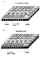
- 基板の一方の側に位置する第1の配線部と、他方の側に位置する第2の配線部とを配線接続する半導体パッケージの製造方法において、
前記第1の配線部に接続される側面電極を形成し、
前記第2の配線部を、基板の上に形成した絶縁層の上に形成し、
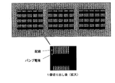
個々の半導体パッケージに個片化するよう完全に切断した際に形成される前記第2の配線部の露出端と、前記側面電極をナノ金属粒子を用いてインクジェット方式により配線したことから成る半導体パッケージの製造方法。 - インクジェット方式による配線を行う前記ナノ金属粒子は、ナノ銅金属粒子であり、このナノ銅金属粒子による配線を、原子状水素により金属表面酸化膜の還元、及び又は、有機物の除去の処理をしたことから成る請求項1に記載の半導体パッケージの製造方法。
- 前記側面電極は、LSI形成面及び前記第1の配線部が位置する基板の一方の側において、該第1の配線部に接続されるポスト電極と同じ高さにして、該ポスト電極と同時に形成し、かつ、ウエハから個々のチップに切断したときに露出するようにチップ端とスクライブラインの両方に跨るように配置し、
個々の半導体パッケージに個片化するよう完全に切断する際、スクライブラインにはみ出した側面電極も同時に切断することにより、パッケージ端面に側面電極を露出させて形成することから成る請求項1に記載の半導体パッケージの製造方法。 - 基板の一方の側には、イメージセンサー形成面と、その上に透明絶縁膜を形成し、この透明絶縁膜を通して外部からの光線が、イメージセンサー形成面の受光素子領域に入射できるようにして、イメージセンサーパッケージを構成することから成る請求項3に半導体パッケージの製造方法。
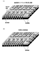
- 前記基板は、有機基板及びその上に接着された半導体チップからなり、
前記第1の配線部は、前記有機基板の最上層に形成されている金属パッド部に接続される前記側面電極を含み、
前記有機基板の配線パターンと電気的接続した半導体チップの上を、一括モールドにより封止して前記絶縁層を形成し、かつ、該絶縁層上に前記第2の配線部を配線し、
個々の半導体パッケージに個片化するよう完全に切断した際に形成される前記第2の配線部の露出端と、前記側面電極との間を、インクジェット方式により配線したことから成る請求項1に記載の半導体パッケージの製造方法。 - 前記絶縁層を形成した後、チップ個片化のための一括モールド部のハーフカットをし、前記第2の配線部は、該ハーフカット部を含めた前記絶縁層上に配線することにより、配線材料を側面の一部に迫出させ、
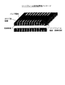
前記側面電極は、このハーフカット部に迫出した配線との間で配線したことから成る請求項5に記載の半導体パッケージの製造方法。 - 前記基板は、リードフレーム及びそのダイパッド上に接着された半導体チップからなり、
前記第1の配線部は、リードフレームのインナーリード部及びアウターリード部を含み、該リードフレームのインナーリード部と電気的接続した半導体チップの上を、一括モールドにより封止して前記絶縁層を形成し、かつ、該絶縁層上に前記第2の配線部を配線し、
リードフレームを周囲の回路と電気的に接続するためのアウターリード部は、その先端断面が、リードフレーム裏面だけでなく、側面にも露出させて前記側面電極とし、
個々の半導体パッケージに個片化するよう完全に切断した際に形成される前記第2の配線部の露出端と、前記側面電極との間を、インクジェット方式により配線したことから成る請求項1に記載の半導体パッケージの製造方法。 - 前記絶縁層を形成した後、チップ個片化のための一括モールド部のハーフカットをし、前記第2の配線部は、該ハーフカット部を含めた前記絶縁層上に配線することにより、配線材料を側面の一部に迫出させ、
前記側面電極は、このハーフカット部に迫出した配線との間で配線したことから成る請求項7に記載の半導体パッケージの製造方法。
Applications Claiming Priority (3)
| Application Number | Priority Date | Filing Date | Title |
|---|---|---|---|
| JP2005127266 | 2005-04-26 | ||
| JP2005127266 | 2005-04-26 | ||
| PCT/JP2006/307087 WO2006117961A1 (ja) | 2005-04-26 | 2006-04-04 | 半導体パッケージ及びその製造方法 |
Publications (2)
| Publication Number | Publication Date |
|---|---|
| JPWO2006117961A1 JPWO2006117961A1 (ja) | 2008-12-18 |
| JP4635209B2 true JP4635209B2 (ja) | 2011-02-23 |
Family
ID=37307767
Family Applications (1)
| Application Number | Title | Priority Date | Filing Date |
|---|---|---|---|
| JP2007514522A Expired - Fee Related JP4635209B2 (ja) | 2005-04-26 | 2006-04-04 | 半導体パッケージの製造方法 |
Country Status (5)
| Country | Link |
|---|---|
| US (1) | US7838983B2 (ja) |
| JP (1) | JP4635209B2 (ja) |
| KR (1) | KR101189100B1 (ja) |
| TW (1) | TW200703589A (ja) |
| WO (1) | WO2006117961A1 (ja) |
Families Citing this family (15)
| Publication number | Priority date | Publication date | Assignee | Title |
|---|---|---|---|---|
| US7939916B2 (en) * | 2007-01-25 | 2011-05-10 | Analog Devices, Inc. | Wafer level CSP packaging concept |
| US7843046B2 (en) * | 2008-02-19 | 2010-11-30 | Vertical Circuits, Inc. | Flat leadless packages and stacked leadless package assemblies |
| JP5033682B2 (ja) * | 2008-03-12 | 2012-09-26 | 株式会社テラミクロス | 半導体素子およびその製造方法並びに半導体装置およびその製造方法 |
| JP2009277970A (ja) * | 2008-05-16 | 2009-11-26 | Fujikura Ltd | 回路配線基板実装体 |
| JP2009277969A (ja) * | 2008-05-16 | 2009-11-26 | Fujikura Ltd | 半導体装置及びその製造方法並びに半導体装置積層体 |
| JP5266009B2 (ja) * | 2008-10-14 | 2013-08-21 | 株式会社フジクラ | 部品内蔵形回路配線基板 |
| CN101930929B (zh) * | 2009-06-26 | 2012-07-18 | 日月光半导体(上海)股份有限公司 | 具有侧表面线路的封装用基板制造方法 |
| CN102804379B (zh) * | 2010-05-24 | 2015-12-09 | 全视科技有限公司 | 双面图像传感器 |
| CN103155136B (zh) | 2010-09-29 | 2015-03-04 | Nxp股份有限公司 | Ic封装件的分离 |
| FR2967814A1 (fr) * | 2010-11-23 | 2012-05-25 | St Microelectronics Grenoble 2 | Dispositif semi-conducteur a puce sur plaque support |
| US9153507B2 (en) * | 2012-01-31 | 2015-10-06 | Broadcom Corporation | Semiconductor package with improved testability |
| JP2014120612A (ja) * | 2012-12-17 | 2014-06-30 | Toshiba Corp | 半導体装置、およびそれを用いた半導体モジュール |
| JP6278251B2 (ja) * | 2013-09-27 | 2018-02-14 | 富士電機株式会社 | 接合組立装置 |
| US9881962B2 (en) * | 2013-12-10 | 2018-01-30 | Sony Corporation | Semiconductor apparatus, solid state imaging device, imaging apparatus and electronic equipment, and manufacturing method thereof |
| US9972558B1 (en) | 2017-04-04 | 2018-05-15 | Stmicroelectronics, Inc. | Leadframe package with side solder ball contact and method of manufacturing |
Citations (3)
| Publication number | Priority date | Publication date | Assignee | Title |
|---|---|---|---|---|
| JP2004303884A (ja) * | 2003-03-31 | 2004-10-28 | Seiko Epson Corp | 三次元実装モジュールの製造方法とその方法で得られる三次元実装モジュール |
| JP2004342883A (ja) * | 2003-05-16 | 2004-12-02 | Oki Electric Ind Co Ltd | 半導体装置、及び半導体装置の製造方法 |
| JP2005005488A (ja) * | 2003-06-12 | 2005-01-06 | Dainippon Printing Co Ltd | 半導体モジュールおよびそれらの製造方法 |
Family Cites Families (7)
| Publication number | Priority date | Publication date | Assignee | Title |
|---|---|---|---|---|
| US5847930A (en) * | 1995-10-13 | 1998-12-08 | Hei, Inc. | Edge terminals for electronic circuit modules |
| JP3599950B2 (ja) * | 1997-04-16 | 2004-12-08 | 株式会社アルバック | 金属ペーストの焼成方法 |
| JP2002075999A (ja) | 2000-08-31 | 2002-03-15 | Ulvac Japan Ltd | 銅配線パターンの形成方法 |
| US7177137B2 (en) * | 2002-04-15 | 2007-02-13 | Avx Corporation | Plated terminations |
| JP3646719B2 (ja) * | 2003-06-19 | 2005-05-11 | セイコーエプソン株式会社 | 半導体装置及びその製造方法、回路基板並びに電子機器 |
| SG120123A1 (en) * | 2003-09-30 | 2006-03-28 | Micron Technology Inc | Castellated chip-scale packages and methods for fabricating the same |
| JP2005340647A (ja) * | 2004-05-28 | 2005-12-08 | Nec Compound Semiconductor Devices Ltd | インターポーザ基板、半導体パッケージ及び半導体装置並びにそれらの製造方法 |
-
2006
- 2006-04-04 WO PCT/JP2006/307087 patent/WO2006117961A1/ja not_active Ceased
- 2006-04-04 JP JP2007514522A patent/JP4635209B2/ja not_active Expired - Fee Related
- 2006-04-04 KR KR1020077024617A patent/KR101189100B1/ko not_active Expired - Fee Related
- 2006-04-04 US US11/911,990 patent/US7838983B2/en active Active
- 2006-04-24 TW TW095114554A patent/TW200703589A/zh not_active IP Right Cessation
Patent Citations (3)
| Publication number | Priority date | Publication date | Assignee | Title |
|---|---|---|---|---|
| JP2004303884A (ja) * | 2003-03-31 | 2004-10-28 | Seiko Epson Corp | 三次元実装モジュールの製造方法とその方法で得られる三次元実装モジュール |
| JP2004342883A (ja) * | 2003-05-16 | 2004-12-02 | Oki Electric Ind Co Ltd | 半導体装置、及び半導体装置の製造方法 |
| JP2005005488A (ja) * | 2003-06-12 | 2005-01-06 | Dainippon Printing Co Ltd | 半導体モジュールおよびそれらの製造方法 |
Also Published As
| Publication number | Publication date |
|---|---|
| US7838983B2 (en) | 2010-11-23 |
| KR20080003832A (ko) | 2008-01-08 |
| JPWO2006117961A1 (ja) | 2008-12-18 |
| KR101189100B1 (ko) | 2012-10-10 |
| WO2006117961A1 (ja) | 2006-11-09 |
| US20090140364A1 (en) | 2009-06-04 |
| TW200703589A (en) | 2007-01-16 |
| TWI305034B (ja) | 2009-01-01 |
Similar Documents
| Publication | Publication Date | Title |
|---|---|---|
| JP4635209B2 (ja) | 半導体パッケージの製造方法 | |
| TWI229435B (en) | Manufacture of semiconductor device | |
| TWI429048B (zh) | 半導體承載元件的製造方法及應用其之半導體封裝件的製造方法 | |
| US8404516B2 (en) | Method for producing a MEMS package | |
| JP3942190B1 (ja) | 両面電極構造の半導体装置及びその製造方法 | |
| US7399683B2 (en) | Manufacturing method of semiconductor device | |
| CN101771013A (zh) | 半导体装置及其制造方法 | |
| WO2007018237A1 (ja) | 半導体装置及びその製造方法 | |
| US10269583B2 (en) | Semiconductor die attachment with embedded stud bumps in attachment material | |
| JP4783906B2 (ja) | パッケージングされた積層型半導体装置及びその製造方法 | |
| CN105938802B (zh) | 树脂密封型半导体装置及其制造方法 | |
| JP2006210758A (ja) | 貫通電極を形成した半導体装置及びその製造方法 | |
| JP4215571B2 (ja) | 半導体装置の製造方法 | |
| JP2005109427A (ja) | 半導体装置及びその製造方法 | |
| JP2003068738A (ja) | 半導体装置及びその製造方法及び半導体チップ及びその実装方法 | |
| JP2012190939A (ja) | 半導体装置およびその製造方法 | |
| TW201737463A (zh) | 半導體裝置及其製造方法 | |
| CN111344860A (zh) | 用于微电子器件的具有保护层的管芯贴合表面铜层 | |
| JP2006202974A (ja) | 電子装置及びその製造方法 | |
| JP6937283B2 (ja) | 半導体装置の製造方法 | |
| JP4483136B2 (ja) | 半導体デバイスの実装方法及び半導体装置の製造方法 | |
| JP4286264B2 (ja) | 半導体装置及びその製造方法 | |
| JP4668608B2 (ja) | 半導体チップおよびそれを用いた半導体装置、ならびに半導体チップの製造方法 | |
| CN104051421A (zh) | 结合基板通孔与金属凸块的半导体晶片结构及其制程方法 | |
| JP2003031722A (ja) | 半導体装置およびその製造方法 |
Legal Events
| Date | Code | Title | Description |
|---|---|---|---|
| A131 | Notification of reasons for refusal |
Free format text: JAPANESE INTERMEDIATE CODE: A131 Effective date: 20100713 |
|
| A521 | Request for written amendment filed |
Free format text: JAPANESE INTERMEDIATE CODE: A523 Effective date: 20100723 |
|
| TRDD | Decision of grant or rejection written | ||
| A01 | Written decision to grant a patent or to grant a registration (utility model) |
Free format text: JAPANESE INTERMEDIATE CODE: A01 Effective date: 20101026 |
|
| A01 | Written decision to grant a patent or to grant a registration (utility model) |
Free format text: JAPANESE INTERMEDIATE CODE: A01 |
|
| R150 | Certificate of patent or registration of utility model |
Free format text: JAPANESE INTERMEDIATE CODE: R150 Ref document number: 4635209 Country of ref document: JP Free format text: JAPANESE INTERMEDIATE CODE: R150 |
|
| S111 | Request for change of ownership or part of ownership |
Free format text: JAPANESE INTERMEDIATE CODE: R313113 |
|
| R350 | Written notification of registration of transfer |
Free format text: JAPANESE INTERMEDIATE CODE: R350 |
|
| R250 | Receipt of annual fees |
Free format text: JAPANESE INTERMEDIATE CODE: R250 |
|
| R250 | Receipt of annual fees |
Free format text: JAPANESE INTERMEDIATE CODE: R250 |
|
| R250 | Receipt of annual fees |
Free format text: JAPANESE INTERMEDIATE CODE: R250 |
|
| R250 | Receipt of annual fees |
Free format text: JAPANESE INTERMEDIATE CODE: R250 |
|
| R250 | Receipt of annual fees |
Free format text: JAPANESE INTERMEDIATE CODE: R250 |
|
| R250 | Receipt of annual fees |
Free format text: JAPANESE INTERMEDIATE CODE: R250 |
|
| R250 | Receipt of annual fees |
Free format text: JAPANESE INTERMEDIATE CODE: R250 |
|
| R250 | Receipt of annual fees |
Free format text: JAPANESE INTERMEDIATE CODE: R250 |
|
| R250 | Receipt of annual fees |
Free format text: JAPANESE INTERMEDIATE CODE: R250 |
|
| LAPS | Cancellation because of no payment of annual fees |