JP4635209B2 - Manufacturing method of semiconductor package - Google Patents
Manufacturing method of semiconductor package Download PDFInfo
- Publication number
- JP4635209B2 JP4635209B2 JP2007514522A JP2007514522A JP4635209B2 JP 4635209 B2 JP4635209 B2 JP 4635209B2 JP 2007514522 A JP2007514522 A JP 2007514522A JP 2007514522 A JP2007514522 A JP 2007514522A JP 4635209 B2 JP4635209 B2 JP 4635209B2
- Authority
- JP
- Japan
- Prior art keywords
- wiring
- electrode
- semiconductor
- substrate
- cut
- Prior art date
- Legal status (The legal status is an assumption and is not a legal conclusion. Google has not performed a legal analysis and makes no representation as to the accuracy of the status listed.)
- Expired - Fee Related
Links
Images


Classifications
-
- H—ELECTRICITY
- H10—SEMICONDUCTOR DEVICES; ELECTRIC SOLID-STATE DEVICES NOT OTHERWISE PROVIDED FOR
- H10W—GENERIC PACKAGES, INTERCONNECTIONS, CONNECTORS OR OTHER CONSTRUCTIONAL DETAILS OF DEVICES COVERED BY CLASS H10
- H10W70/00—Package substrates; Interposers; Redistribution layers [RDL]
- H10W70/40—Leadframes
- H10W70/421—Shapes or dispositions
- H10W70/424—Cross-sectional shapes
-
- H—ELECTRICITY
- H10—SEMICONDUCTOR DEVICES; ELECTRIC SOLID-STATE DEVICES NOT OTHERWISE PROVIDED FOR
- H10P—GENERIC PROCESSES OR APPARATUS FOR THE MANUFACTURE OR TREATMENT OF DEVICES COVERED BY CLASS H10
- H10P74/00—Testing or measuring during manufacture or treatment of wafers, substrates or devices
- H10P74/27—Structural arrangements therefor
- H10P74/273—Interconnections for measuring or testing, e.g. probe pads
-
- H—ELECTRICITY
- H10—SEMICONDUCTOR DEVICES; ELECTRIC SOLID-STATE DEVICES NOT OTHERWISE PROVIDED FOR
- H10W—GENERIC PACKAGES, INTERCONNECTIONS, CONNECTORS OR OTHER CONSTRUCTIONAL DETAILS OF DEVICES COVERED BY CLASS H10
- H10W20/00—Interconnections in chips, wafers or substrates
- H10W20/20—Interconnections within wafers or substrates, e.g. through-silicon vias [TSV]
-
- H—ELECTRICITY
- H10—SEMICONDUCTOR DEVICES; ELECTRIC SOLID-STATE DEVICES NOT OTHERWISE PROVIDED FOR
- H10W—GENERIC PACKAGES, INTERCONNECTIONS, CONNECTORS OR OTHER CONSTRUCTIONAL DETAILS OF DEVICES COVERED BY CLASS H10
- H10W70/00—Package substrates; Interposers; Redistribution layers [RDL]
- H10W70/60—Insulating or insulated package substrates; Interposers; Redistribution layers
- H10W70/62—Insulating or insulated package substrates; Interposers; Redistribution layers characterised by their interconnections
- H10W70/65—Shapes or dispositions of interconnections
- H10W70/657—Shapes or dispositions of interconnections on sidewalls or bottom surfaces of the package substrates, interposers or redistribution layers
-
- H—ELECTRICITY
- H10—SEMICONDUCTOR DEVICES; ELECTRIC SOLID-STATE DEVICES NOT OTHERWISE PROVIDED FOR
- H10W—GENERIC PACKAGES, INTERCONNECTIONS, CONNECTORS OR OTHER CONSTRUCTIONAL DETAILS OF DEVICES COVERED BY CLASS H10
- H10W72/00—Interconnections or connectors in packages
-
- H—ELECTRICITY
- H10—SEMICONDUCTOR DEVICES; ELECTRIC SOLID-STATE DEVICES NOT OTHERWISE PROVIDED FOR
- H10W—GENERIC PACKAGES, INTERCONNECTIONS, CONNECTORS OR OTHER CONSTRUCTIONAL DETAILS OF DEVICES COVERED BY CLASS H10
- H10W74/00—Encapsulations, e.g. protective coatings
- H10W74/10—Encapsulations, e.g. protective coatings characterised by their shape or disposition
- H10W74/111—Encapsulations, e.g. protective coatings characterised by their shape or disposition the semiconductor body being completely enclosed
- H10W74/129—Encapsulations, e.g. protective coatings characterised by their shape or disposition the semiconductor body being completely enclosed forming a chip-scale package [CSP]
-
- H—ELECTRICITY
- H10—SEMICONDUCTOR DEVICES; ELECTRIC SOLID-STATE DEVICES NOT OTHERWISE PROVIDED FOR
- H10W—GENERIC PACKAGES, INTERCONNECTIONS, CONNECTORS OR OTHER CONSTRUCTIONAL DETAILS OF DEVICES COVERED BY CLASS H10
- H10W90/00—Package configurations
-
- H—ELECTRICITY
- H10—SEMICONDUCTOR DEVICES; ELECTRIC SOLID-STATE DEVICES NOT OTHERWISE PROVIDED FOR
- H10W—GENERIC PACKAGES, INTERCONNECTIONS, CONNECTORS OR OTHER CONSTRUCTIONAL DETAILS OF DEVICES COVERED BY CLASS H10
- H10W90/00—Package configurations
- H10W90/701—Package configurations characterised by the relative positions of pads or connectors relative to package parts
-
- B—PERFORMING OPERATIONS; TRANSPORTING
- B82—NANOTECHNOLOGY
- B82Y—SPECIFIC USES OR APPLICATIONS OF NANOSTRUCTURES; MEASUREMENT OR ANALYSIS OF NANOSTRUCTURES; MANUFACTURE OR TREATMENT OF NANOSTRUCTURES
- B82Y99/00—Subject matter not provided for in other groups of this subclass
-
- H—ELECTRICITY
- H10—SEMICONDUCTOR DEVICES; ELECTRIC SOLID-STATE DEVICES NOT OTHERWISE PROVIDED FOR
- H10W—GENERIC PACKAGES, INTERCONNECTIONS, CONNECTORS OR OTHER CONSTRUCTIONAL DETAILS OF DEVICES COVERED BY CLASS H10
- H10W70/00—Package substrates; Interposers; Redistribution layers [RDL]
- H10W70/40—Leadframes
-
- H—ELECTRICITY
- H10—SEMICONDUCTOR DEVICES; ELECTRIC SOLID-STATE DEVICES NOT OTHERWISE PROVIDED FOR
- H10W—GENERIC PACKAGES, INTERCONNECTIONS, CONNECTORS OR OTHER CONSTRUCTIONAL DETAILS OF DEVICES COVERED BY CLASS H10
- H10W70/00—Package substrates; Interposers; Redistribution layers [RDL]
- H10W70/60—Insulating or insulated package substrates; Interposers; Redistribution layers
-
- H—ELECTRICITY
- H10—SEMICONDUCTOR DEVICES; ELECTRIC SOLID-STATE DEVICES NOT OTHERWISE PROVIDED FOR
- H10W—GENERIC PACKAGES, INTERCONNECTIONS, CONNECTORS OR OTHER CONSTRUCTIONAL DETAILS OF DEVICES COVERED BY CLASS H10
- H10W72/00—Interconnections or connectors in packages
- H10W72/01—Manufacture or treatment
- H10W72/0198—Manufacture or treatment batch processes
-
- H—ELECTRICITY
- H10—SEMICONDUCTOR DEVICES; ELECTRIC SOLID-STATE DEVICES NOT OTHERWISE PROVIDED FOR
- H10W—GENERIC PACKAGES, INTERCONNECTIONS, CONNECTORS OR OTHER CONSTRUCTIONAL DETAILS OF DEVICES COVERED BY CLASS H10
- H10W72/00—Interconnections or connectors in packages
- H10W72/50—Bond wires
- H10W72/541—Dispositions of bond wires
- H10W72/5449—Dispositions of bond wires not being orthogonal to a side surface of the chip, e.g. fan-out arrangements
-
- H—ELECTRICITY
- H10—SEMICONDUCTOR DEVICES; ELECTRIC SOLID-STATE DEVICES NOT OTHERWISE PROVIDED FOR
- H10W—GENERIC PACKAGES, INTERCONNECTIONS, CONNECTORS OR OTHER CONSTRUCTIONAL DETAILS OF DEVICES COVERED BY CLASS H10
- H10W72/00—Interconnections or connectors in packages
- H10W72/50—Bond wires
- H10W72/551—Materials of bond wires
- H10W72/552—Materials of bond wires comprising metals or metalloids, e.g. silver
- H10W72/5522—Materials of bond wires comprising metals or metalloids, e.g. silver comprising gold [Au]
-
- H—ELECTRICITY
- H10—SEMICONDUCTOR DEVICES; ELECTRIC SOLID-STATE DEVICES NOT OTHERWISE PROVIDED FOR
- H10W—GENERIC PACKAGES, INTERCONNECTIONS, CONNECTORS OR OTHER CONSTRUCTIONAL DETAILS OF DEVICES COVERED BY CLASS H10
- H10W72/00—Interconnections or connectors in packages
- H10W72/851—Dispositions of multiple connectors or interconnections
- H10W72/874—On different surfaces
- H10W72/884—Die-attach connectors and bond wires
-
- H—ELECTRICITY
- H10—SEMICONDUCTOR DEVICES; ELECTRIC SOLID-STATE DEVICES NOT OTHERWISE PROVIDED FOR
- H10W—GENERIC PACKAGES, INTERCONNECTIONS, CONNECTORS OR OTHER CONSTRUCTIONAL DETAILS OF DEVICES COVERED BY CLASS H10
- H10W74/00—Encapsulations, e.g. protective coatings
-
- H—ELECTRICITY
- H10—SEMICONDUCTOR DEVICES; ELECTRIC SOLID-STATE DEVICES NOT OTHERWISE PROVIDED FOR
- H10W—GENERIC PACKAGES, INTERCONNECTIONS, CONNECTORS OR OTHER CONSTRUCTIONAL DETAILS OF DEVICES COVERED BY CLASS H10
- H10W74/00—Encapsulations, e.g. protective coatings
- H10W74/10—Encapsulations, e.g. protective coatings characterised by their shape or disposition
- H10W74/15—Encapsulations, e.g. protective coatings characterised by their shape or disposition on active surfaces of flip-chip devices, e.g. underfills
-
- H—ELECTRICITY
- H10—SEMICONDUCTOR DEVICES; ELECTRIC SOLID-STATE DEVICES NOT OTHERWISE PROVIDED FOR
- H10W—GENERIC PACKAGES, INTERCONNECTIONS, CONNECTORS OR OTHER CONSTRUCTIONAL DETAILS OF DEVICES COVERED BY CLASS H10
- H10W90/00—Package configurations
- H10W90/701—Package configurations characterised by the relative positions of pads or connectors relative to package parts
- H10W90/721—Package configurations characterised by the relative positions of pads or connectors relative to package parts of bump connectors
- H10W90/722—Package configurations characterised by the relative positions of pads or connectors relative to package parts of bump connectors between stacked chips
-
- H—ELECTRICITY
- H10—SEMICONDUCTOR DEVICES; ELECTRIC SOLID-STATE DEVICES NOT OTHERWISE PROVIDED FOR
- H10W—GENERIC PACKAGES, INTERCONNECTIONS, CONNECTORS OR OTHER CONSTRUCTIONAL DETAILS OF DEVICES COVERED BY CLASS H10
- H10W90/00—Package configurations
- H10W90/701—Package configurations characterised by the relative positions of pads or connectors relative to package parts
- H10W90/721—Package configurations characterised by the relative positions of pads or connectors relative to package parts of bump connectors
- H10W90/724—Package configurations characterised by the relative positions of pads or connectors relative to package parts of bump connectors between a chip and a stacked insulating package substrate, interposer or RDL
-
- H—ELECTRICITY
- H10—SEMICONDUCTOR DEVICES; ELECTRIC SOLID-STATE DEVICES NOT OTHERWISE PROVIDED FOR
- H10W—GENERIC PACKAGES, INTERCONNECTIONS, CONNECTORS OR OTHER CONSTRUCTIONAL DETAILS OF DEVICES COVERED BY CLASS H10
- H10W90/00—Package configurations
- H10W90/701—Package configurations characterised by the relative positions of pads or connectors relative to package parts
- H10W90/731—Package configurations characterised by the relative positions of pads or connectors relative to package parts of die-attach connectors
- H10W90/734—Package configurations characterised by the relative positions of pads or connectors relative to package parts of die-attach connectors between a chip and a stacked insulating package substrate, interposer or RDL
-
- H—ELECTRICITY
- H10—SEMICONDUCTOR DEVICES; ELECTRIC SOLID-STATE DEVICES NOT OTHERWISE PROVIDED FOR
- H10W—GENERIC PACKAGES, INTERCONNECTIONS, CONNECTORS OR OTHER CONSTRUCTIONAL DETAILS OF DEVICES COVERED BY CLASS H10
- H10W90/00—Package configurations
- H10W90/701—Package configurations characterised by the relative positions of pads or connectors relative to package parts
- H10W90/751—Package configurations characterised by the relative positions of pads or connectors relative to package parts of bond wires
- H10W90/754—Package configurations characterised by the relative positions of pads or connectors relative to package parts of bond wires between a chip and a stacked insulating package substrate, interposer or RDL
Landscapes
- Internal Circuitry In Semiconductor Integrated Circuit Devices (AREA)
- Solid State Image Pick-Up Elements (AREA)
Abstract
Description
本発明は、基板の一方の側に位置する配線部と、他方の側に位置する配線部とを、ナノ金属粒子を用いてインクジェット方式により側面で配線接続する半導体パッケージの製造方法に関する。
The present invention includes a wiring portion located on one side of the substrate, and a wiring portion located on the other side, a method of manufacturing a semiconductor package to the wiring connection side by an inkjet method using a nano-metal particles.
LSIチップの高集積化に伴い、パッケージサイズの縮小化も強く要求されており、様々な実装パッケージ構造が提案されている。近年、半導体ベアチップに貫通電極を形成して積層しようとする開発が盛んに行われている。一方、リアルサイズの両面電極パッケージもこれから製品化される可能性が高い。いずれの技術においても、従来の両面電極パッケージは常に貫通電極構造を必要としているが、現在の貫通孔の絶縁方法は、高温で処理されるため半導体の実装プロセスへの適用は困難であった。このように、半導体基板への貫通孔の形成とその絶縁方法にはまだ課題が残されていて、貫通電極を必要とせずに配線することが望まれる。 Along with the high integration of LSI chips, there is a strong demand for reducing the package size, and various mounting package structures have been proposed. 2. Description of the Related Art In recent years, developments for forming and stacking through electrodes on a semiconductor bare chip have been actively conducted. On the other hand, real size double-sided electrode packages are also likely to be commercialized. In any of the techniques, the conventional double-sided electrode package always requires a through electrode structure. However, since the current through hole insulation method is processed at a high temperature, it is difficult to apply it to a semiconductor mounting process. As described above, there is still a problem in the formation of the through hole in the semiconductor substrate and the insulating method thereof, and it is desired to perform wiring without requiring the through electrode.
一方、近年、ナノ金属粒子が開発されている。材料としては銅、銀、金等がある。これらの微粒子はインクジェット方式で直接描画できることに大きな特長がある。有機溶媒中にナノ金属粒子が含有されており、それをプリンターで実用されているインクジェット法で所望のパターンを描く方法である。銀や金のような貴金属はもともと酸化されにくいが、銅の場合は銀や金と比較すると酸化されやすい性質を持つ。配線パターン描画後は、有機溶媒を蒸発させ、さらに銅粒子同士を付着させる熱処理(200〜300℃程度)が必要である。しかしながら、その熱処理中にも銅の表面は酸化されてしまう。ナノ金属粒子では表面部分の原子の割合が大きいので、表面酸化銅形成により配線抵抗が大きくなるという問題点がある。 Meanwhile, in recent years, nano metal particles have been developed. Examples of the material include copper, silver, and gold. These fine particles have a great feature that they can be drawn directly by an ink jet method. In this method, nano metal particles are contained in an organic solvent, and a desired pattern is drawn by an ink jet method that is practically used in a printer. Precious metals such as silver and gold are not easily oxidized, but copper is more easily oxidized than silver and gold. After drawing the wiring pattern, a heat treatment (about 200 to 300 ° C.) for evaporating the organic solvent and adhering the copper particles is necessary. However, the copper surface is oxidized during the heat treatment. Since the ratio of atoms in the surface portion of nano metal particles is large, there is a problem that the wiring resistance increases due to the formation of surface copper oxide.
また、熱処理だけでは有機溶媒を十分に取り除くことができないため、銅配線の抵抗率を下げられずに、配線として利用できないのが現状である。描画後の低抵抗化に関して、特に銅ではまだ十分な解決法が見出されていない。 Moreover, since the organic solvent cannot be sufficiently removed only by heat treatment, the resistivity of the copper wiring cannot be lowered and cannot be used as wiring. Regarding the reduction in resistance after drawing, a sufficient solution has not yet been found, particularly with copper.
インクジェット方式等の直描方式ではなく、レジストに混合してリソグラフィを使う技術においては、銅の低抵抗化は色々と提案されており、例えば、特許文献1が知られている。ここで使っている還元熱処理技術は、4%以下の分子状(H2)水素を含んだ不活性ガス中(または真空中)で、200〜450℃の温度で行っている。このように、この技術は、銅の微粒子は使用するものの、直描方式ではなく、還元の温度が200〜450℃と高くなっている。これだけ高温だと半導体の実装領域では使用することは困難である。
本発明は、係る問題点を解決して、貫通電極技術を必要とすること無く、容易に両面電極パッケージを製造し、供給することを目的としている。これによって、ウエハレベルタイプ両面電極パッケージ、リードフレームタイプ両面電極パッケージ、或いは有機基板型両面電極パッケージ(BGAタイプ)の製造を可能にして、従来の携帯電話への応用以外に各種センサー(音、磁気、圧力、等)用パッケージとしても有効となる。 An object of the present invention is to solve such problems and easily manufacture and supply a double-sided electrode package without requiring a through electrode technique. This makes it possible to manufacture wafer-level double-sided electrode packages, lead frame-type double-sided electrode packages, or organic substrate-type double-sided electrode packages (BGA type). , Pressure, etc.).
また、本発明は、ナノ金属粒子を用いたインクジェット方式で側面配線を形成する。特に、銅を用いた際には、表面酸化銅形成により配線抵抗が大きくなるという問題点を解決して、描画後の低抵抗化を図り、半導体に実装可能にすることを目的としている。 Further, in the present invention, the side wiring is formed by an ink jet method using nano metal particles. In particular, when copper is used, the object is to solve the problem of increasing the wiring resistance due to the formation of surface copper oxide, to reduce the resistance after drawing, and to enable mounting on a semiconductor.
本発明の半導体パッケージの製造方法は、基板の一方の側に位置する第1の配線部と、他方の側に位置する第2の配線部とを配線接続する。第1の配線部に接続される側面電極を形成し、第2の配線部を、基板の上に形成した絶縁層の上に形成する。個々の半導体パッケージに個片化するよう完全に切断した際に形成される第2の配線部の露出端と、側面電極をナノ金属粒子を用いてインクジェット方式により配線する。インクジェット方式による配線を行うナノ金属粒子は、ナノ銅金属粒子であり、このナノ銅金属粒子による配線を、原子状水素により金属表面酸化膜の還元、及び又は、有機物の除去の処理をする。
The method of manufacturing a semiconductor package of the present invention, the wiring connected to the first wiring portion located on one side of the substrate, and the second wiring portion located on the other side. A side electrode connected to the first wiring portion is formed, and a second wiring portion is formed on the insulating layer formed on the substrate. The exposed end of the second wiring portion formed when completely cut into individual semiconductor packages and the side electrode are wired by an inkjet method using nano metal particles. The nano metal particles to be wired by the ink jet method are nano copper metal particles, and the wiring by the nano copper metal particles is subjected to reduction of the metal surface oxide film and / or removal of organic substances by atomic hydrogen.
本発明の半導体パッケージの製造方法は、LSI形成面及び第1の配線部が位置する基板の一方の側において、側面電極を、該第1の配線部に接続されるポスト電極と同じ高さにして、該ポスト電極と同時に形成し、かつ、ウエハから個々のチップに切断したときに露出するようにチップ端とスクライブラインの両方に跨るように配置する。個々の半導体パッケージに個片化するよう完全に切断する際、スクライブラインにはみ出した側面電極も同時に切断することにより、パッケージ端面に側面電極を露出させて形成する。
Semiconductor package manufacturing method of the di of the present invention, one side of the substrate on which an LSI formation surface and the first wiring portion is positioned, the same height as the post electrodes to be connected to the side electrode, the wiring portion of the first Then, it is formed at the same time as the post electrode, and is arranged so as to straddle both the chip end and the scribe line so as to be exposed when the wafer is cut into individual chips. When completely cutting each individual semiconductor package into pieces, the side electrode protruding from the scribe line is also cut at the same time, so that the side electrode is exposed at the package end surface.
基板の一方の側には、イメージセンサー形成面と、その上に透明絶縁膜を形成し、この透明絶縁膜を通して外部からの光線が、イメージセンサー形成面の受光素子領域に入射できるようにして、イメージセンサーパッケージを構成することができる。 On one side of the substrate, an image sensor forming surface and a transparent insulating film are formed on the surface. Through this transparent insulating film, light from the outside can enter the light receiving element region of the image sensor forming surface, An image sensor package can be configured.
また、本発明の半導体パッケージの製造方法は、基板を、有機基板及びその上に接着された半導体チップから構成する。第1の配線部は、有機基板の最上層に形成されている金属パッド部に接続される側面電極を含み、有機基板の配線パターンと電気的接続した半導体チップの上を、一括モールドにより封止して絶縁層を形成し、かつ、該絶縁層上に第2の配線部を配線する。個々の半導体パッケージに個片化するよう完全に切断した際に形成される第2の配線部の露出端と、側面電極との間を、インクジェット方式により配線する。
A method of manufacturing a semiconductor package of the present invention, the substrate is composed of a semiconductor chip adhered to the organic substrate and thereon. The first wiring portion includes a side electrode connected to a metal pad portion formed on the uppermost layer of the organic substrate, and the semiconductor chip electrically connected to the wiring pattern of the organic substrate is sealed by a collective mold Then, an insulating layer is formed, and a second wiring portion is wired on the insulating layer. Wiring is performed by an inkjet method between the exposed end of the second wiring portion formed when completely cut into individual semiconductor packages and the side electrodes.
また、本発明の半導体パッケージの製造方法は、基板を、リードフレーム及びそのダイパッド上に接着された半導体チップから構成する。第1の配線部は、リードフレームのインナーリード部及びアウターリード部を含み、該リードフレームのインナーリード部と電気的接続した半導体チップの上を、一括モールドにより封止して絶縁層を形成し、かつ、該絶縁層上に第2の配線部を配線する。リードフレームを周囲の回路と電気的に接続するためのアウターリード部は、その先端断面が、リードフレーム裏面だけでなく、側面にも露出させて側面電極とする。個々の半導体パッケージに個片化するよう完全に切断した際に形成される第2の配線部の露出端と、側面電極との間を、インクジェット方式により配線する。
The semiconductor package manufacturing method of the di of the present invention constitutes a substrate, a semiconductor chip adhered to the lead frame and the die pad. The first wiring portion includes an inner lead portion and an outer lead portion of the lead frame, and an insulating layer is formed by sealing the semiconductor chip electrically connected to the inner lead portion of the lead frame by collective molding. And a 2nd wiring part is wired on this insulating layer. The outer lead portion for electrically connecting the lead frame to the surrounding circuit has a tip cross section exposed not only on the back surface of the lead frame but also on the side surface to form a side electrode. Wiring is performed by an inkjet method between the exposed end of the second wiring portion formed when completely cut into individual semiconductor packages and the side electrodes.
本発明によれば、貫通孔を形成しなくても両面電極パッケージが可能となるため、従来の携帯電話への応用以外に各種センサー(音、磁気、圧力、等)用パッケージとしても有効となる。 According to the present invention, since a double-sided electrode package is possible without forming a through hole, it is effective as a package for various sensors (sound, magnetism, pressure, etc.) in addition to application to a conventional mobile phone. .
本発明は、携帯電話等、高密度実装を必要としている機器において、比較的大きなチップサイズ(例えば5mm□以上)で貫通電極技術を必要とすること無く、容易にウエハレベルタイプ両面電極パッケージを製造し、供給することができる。 The present invention easily manufactures a wafer level type double-sided electrode package with a relatively large chip size (for example, 5 mm □ or more) without requiring a through electrode technology in a device such as a cellular phone that requires high-density mounting. Can be supplied.
また、本発明によれば、チップサイズが小さくウエハレベルでは対応できない分野にも対応可能なリードフレームタイプ両面電極パッケージ或いは有機基板型両面電極パッケージ(BGAタイプ)を提供して、例えばマイク直結のDSP用パッケージや磁気センサー、圧力センサーなど処理プロセッサーのチップサイズが小さいLSIに有効である。通常のリードフレーム技術が使えるので安いコストで提供可能となる。 Further, according to the present invention, a lead frame type double-sided electrode package or an organic substrate type double-sided electrode package (BGA type) that can be used in fields where the chip size is small and cannot be handled at the wafer level is provided. This is effective for LSIs with small processing processor chip size, such as packaging, magnetic sensors, and pressure sensors. Since normal lead frame technology can be used, it can be provided at a low cost.
また、本発明によれば、Hot-Wire法の金属触媒で分解した原子状の水素(H)で、減圧下で還元を行うので、その還元活性が分子状の水素より遥かに高く、そのために、還元温度はより低温で可能となる。これによって、本発明は、半導体装置の製造に適用して、特に、銅を用いて配線描画した後の低抵抗化を図ることが可能となる。 In addition, according to the present invention, reduction is performed under reduced pressure with atomic hydrogen (H) decomposed by a metal catalyst of the Hot-Wire method, so that the reduction activity is much higher than that of molecular hydrogen. The reduction temperature is possible at a lower temperature. As a result, the present invention can be applied to the manufacture of semiconductor devices, and in particular, the resistance can be reduced after wiring drawing using copper.
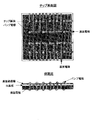
以下、例示に基づき本発明を説明する。図1及び図2は、本発明の両面電極パッケージを、ウエハレベル半導体に適用した第1の例を示すチップ上面図及び裏面図をそれぞれ示している。半導体装置の製造においては、厚さ数100μmの半導体基板を用意した後、この半導体基板の上面(第1の主面)のLSI形成面に回路(回路素子)を形成する。また、半導体基板の上面には多層配線部が形成される。以下の説明において、半導体(Si)基板上に形成されるLSI形成面及び多層配線部が位置する側を、上面側と称し、その反対側を裏面(第2の主面)側と称している。 Hereinafter, the present invention will be described based on examples. 1 and 2 are a top view and a back view, respectively, showing a first example in which the double-sided electrode package of the present invention is applied to a wafer level semiconductor. In the manufacture of a semiconductor device, after preparing a semiconductor substrate having a thickness of several hundreds of micrometers, a circuit (circuit element) is formed on the LSI formation surface on the upper surface (first main surface) of the semiconductor substrate. A multilayer wiring portion is formed on the upper surface of the semiconductor substrate. In the following description, the side on which the LSI formation surface and the multilayer wiring portion formed on the semiconductor (Si) substrate are located is referred to as the upper surface side, and the opposite side is referred to as the back surface (second main surface) side. .
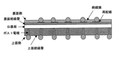
例示の両面電極パッケージは、上面側と裏面側を接続する側面配線に特徴を有している。Si基板の上面側においては、LSI形成面及び多層配線部(LSI上面再配線)が形成され(図示省略)、さらに、このLSI上面再配線上の所定位置に接続するために、そこに柱状のCuポスト電極(図3参照)を複数形成する。このポスト電極は、上面絶縁層で覆うと共に、その先端には、外部接続用のバンプ電極が設けられる。 The illustrated double-sided electrode package is characterized by side wiring that connects the upper surface side and the back surface side. On the upper surface side of the Si substrate, an LSI formation surface and a multi-layer wiring portion (LSI upper surface rewiring) are formed (not shown), and further, a columnar shape is formed there to connect to a predetermined position on the LSI upper surface rewiring. A plurality of Cu post electrodes (see FIG. 3) are formed. The post electrode is covered with an upper insulating layer, and a bump electrode for external connection is provided at the tip.
一方、図2に例示するSi基板の裏面側においては、裏面絶縁層を塗布する。この裏面絶縁層の上に、裏面再配線を実施する。この裏面再配線は、本発明の特徴とする側面配線を通して、上面側の多層配線部の所望箇所に接続される。この側面配線は、上面側に形成された側面電極と、裏面側において形成された裏面電極をインクジェット方式により接続することにより行われるが、その詳細は後述する。裏面再配線の上に、保護膜が塗布される。さらに、再配線上のバンプ形成部上の保護膜に開口を設け、ここに、バンプ電極を形成する。 On the other hand, a back insulating layer is applied on the back side of the Si substrate illustrated in FIG. Back surface rewiring is performed on the back surface insulating layer. The rear surface rewiring is connected to a desired portion of the multilayer wiring portion on the upper surface side through the side surface wiring characterizing the present invention. The side surface wiring is performed by connecting the side surface electrode formed on the upper surface side and the back surface electrode formed on the back surface side by an ink jet method, and details thereof will be described later. A protective film is applied on the back surface rewiring. Further, an opening is provided in the protective film on the bump forming portion on the rewiring, and a bump electrode is formed here.
これによって、上面側と裏面側の両面に外部接続用のバンプ電極を備えて、他の半導体装置等と積層して用いることのできる積層型半導体装置が構成される。 As a result, a stacked semiconductor device is configured that includes bump electrodes for external connection on both the upper surface side and the back surface side, and can be used by being stacked with other semiconductor devices.
次に、このような積層型半導体装置の製造について、半導体装置をポスト電極部で切断した断面図を示す図3を参照してさらに説明する。半導体装置の製造においては、厚さ数100μmの半導体(Si)基板を用意した後、この半導体基板の上面側のLSI形成面に回路(回路素子)を形成し、またその上には、リソグラフィ、インクジェット等の手段により多層配線部(再配線部)が形成される(図示省略)。この多層配線部を介して、後述するように形成されるポスト電極と側面電極が接続される。 Next, the manufacture of such a stacked semiconductor device will be further described with reference to FIG. 3 showing a cross-sectional view of the semiconductor device cut at the post electrode portion. In the manufacture of a semiconductor device, after preparing a semiconductor (Si) substrate having a thickness of several hundreds of μm, a circuit (circuit element) is formed on an LSI formation surface on the upper surface side of the semiconductor substrate. A multilayer wiring portion (rewiring portion) is formed by means such as ink jet (not shown). A post electrode and a side electrode formed as described later are connected through the multilayer wiring portion.
この半導体基板の上面側において、多層配線部の所定位置に接続するために、そこに柱状のCuポスト電極、及びそれと同じ高さの側面電極(図1或いは図6参照)をそれぞれ複数同時に形成する。側面電極は、ウエハから個々のチップに切断したときに露出するようにチップ端とスクライブラインの両方に跨るように配置される。 In order to connect to a predetermined position of the multilayer wiring portion on the upper surface side of the semiconductor substrate, a plurality of columnar Cu post electrodes and side electrodes (see FIG. 1 or FIG. 6) having the same height are simultaneously formed there. . The side electrode is disposed so as to straddle both the chip end and the scribe line so as to be exposed when the wafer is cut into individual chips.
つぎに、図3に示すように、半導体基板の上面に上面絶縁層を形成する。ポスト電極は上面絶縁層に覆われる。上面絶縁層は、エポキシ樹脂やポリイミド樹脂等絶縁性の有機樹脂が使用される。上面絶縁層は、例えば、プラスチックモールド(ウエハ上面モールド)によって形成する。つぎに、上面絶縁層の表面を、ポスト電極の先端が露出するように研磨する。研磨量が多ければ、ポスト電極の厚さが短くなり、上面絶縁層の厚さも薄くなる。 Next, as shown in FIG. 3, an upper surface insulating layer is formed on the upper surface of the semiconductor substrate. The post electrode is covered with an upper surface insulating layer. For the top insulating layer, an insulating organic resin such as an epoxy resin or a polyimide resin is used. The upper surface insulating layer is formed by, for example, a plastic mold (wafer upper surface mold). Next, the surface of the upper insulating layer is polished so that the tip of the post electrode is exposed. If the polishing amount is large, the thickness of the post electrode is shortened, and the thickness of the upper insulating layer is also reduced.
後の工程で行われる側面配線は、シリコン基板の側面でインクジェット方式により行われるために、シリコン基板を研削する必要は必ずしもないが、上面モールド面を支持体にしてシリコン基板を、例えば100μm前後まで研削して、シリコン基板厚さを薄くしても、上面絶縁層が厚く剛性作用が働きウエハ全体の強度が維持できる。 Side wiring performed in the subsequent process is performed by an ink jet method on the side surface of the silicon substrate, so it is not always necessary to grind the silicon substrate, but the silicon substrate is supported up to about 100 μm, for example, with the upper mold surface as a support. Even if the silicon substrate is thinned by grinding, the upper surface insulating layer is thick and has a rigid action, so that the strength of the entire wafer can be maintained.
つぎに、半導体基板の裏面側において、裏面絶縁層を形成する。裏面絶縁層の厚さは、最低でも電気的絶縁を図ることができる厚さにする。この段階で、この裏面絶縁層を上にして、ウエハからチップをハーフカットしても良い。但し、ハーフカットにより形成された溝内に、後の工程で入り込んだ配線材料がシリコン基板とショートすることが無いように、ハーフカットは裏面絶縁層の途中までにする。 Next, a back surface insulating layer is formed on the back surface side of the semiconductor substrate. The thickness of the back surface insulating layer is set to a thickness at which electrical insulation can be achieved at a minimum. At this stage, the chip may be half-cut from the wafer with the back insulating layer facing up. However, the half-cut is made halfway along the back surface insulating layer so that the wiring material that has entered in the groove formed by the half-cut does not short-circuit with the silicon substrate.
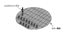
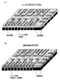
次に、この裏面絶縁層の上に、裏面電極用配線(再配線)を実施する。この裏面電極用配線は、インクジェット方式により行う。上述のハーフカットがなされている場合は、ハーフカットにより形成された溝内にも配線材料が入り込む。半導体装置の製造においては、一般に、面積が広い半導体ウエハが用意され、その後、各処理を経て、最終的には縦横に切断分離して多数の半導体素子(半導体チップ)を形成することになるが、図4は、この半導体ウエハの裏面に対して、ナノ金属粒子を用いてインクジェットで行う再配線を示している。或いは、この再配線はスクリーン印刷でも行うことができる。 Next, back electrode wiring (rewiring) is performed on the back insulating layer. The back electrode wiring is performed by an ink jet method. When the above-described half cut is performed, the wiring material enters the groove formed by the half cut. In the manufacture of a semiconductor device, generally, a semiconductor wafer having a large area is prepared, and after that, through each process, finally, a large number of semiconductor elements (semiconductor chips) are formed by cutting and separating vertically and horizontally. FIG. 4 shows rewiring performed by inkjet using nano metal particles on the back surface of the semiconductor wafer. Alternatively, this rewiring can be performed by screen printing.
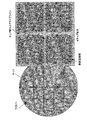
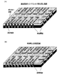
つぎに、チップは完全に切断される。図5は、このようなチップの切断を説明する図である。面積が広い半導体ウエハの上面に、所定の回路素子を含む単位回路が形成される。この単位回路はウエハの上面に縦横に整列配置形成される。その後も、ウエハレベルで、上述したポスト電極、側面電極の形成とか絶縁膜の形成を含む各処理を行う。そして、最終的には縦横に切断分離して多数の半導体素子(半導体チップ)を形成することになる。側面電極は、上述したように、ウエハから個々のチップに切断したときに露出するようにチップ端とスクライブラインの両方に跨るように配置されている。 Next, the chip is completely cut. FIG. 5 is a diagram illustrating such cutting of the chip. A unit circuit including predetermined circuit elements is formed on the upper surface of a semiconductor wafer having a large area. The unit circuits are aligned and formed vertically and horizontally on the upper surface of the wafer. Thereafter, each process including the formation of the post electrode and the side electrode and the formation of the insulating film is performed at the wafer level. Finally, a large number of semiconductor elements (semiconductor chips) are formed by cutting and separating vertically and horizontally. As described above, the side electrode is disposed so as to straddle both the chip end and the scribe line so as to be exposed when the wafer is cut into individual chips.
図6は、ハーフカットがなされている場合について、完全に切断した状態のチップ切出し後を示す図(A)、及びシリコン基板切断側面の全面に絶縁を施した後に側面配線した完成図(B)を示している。図7は、図6と同様なチップ切出し後を示す図(A)、及び絶縁後に側面配線した完成図(B)を示しているが、ハーフカットすること無く完全に切断した場合を示している。図8は、図7と同様な図であるが、シリコン基板切断側面の絶縁を必要な箇所のみに施した図(A)、及び側面配線後の完成図(B)を示している。 FIG. 6A is a diagram illustrating a case where a half cut has been performed, after cutting the chip in a completely cut state, and a completed diagram in which side wiring is performed after insulating the entire side surface of the silicon substrate. Is shown. FIG. 7 shows a view (A) showing a chip cutout similar to FIG. 6 and a completed drawing (B) in which side wiring is performed after insulation, and shows a case where the chip is completely cut without half-cutting. . FIG. 8 is a view similar to FIG. 7, but shows a view (A) in which the insulation of the cut side surface of the silicon substrate is applied only to necessary portions, and a completed view (B) after the side wiring.
上述したハーフカットが、図6に示すようになされている場合、この完全切断時のブレードの歯は、ハーフカットより狭いものを用いる。また、図7及び図8に示すように、ハーフカットすること無く、個々のチップに完全に切断することも可能である。いずれの場合も、完全に切断したときにはスクライブラインにはみ出した側面電極も同時に切断し、チップ端面に側面電極が露出する。裏面電極とは、ハーフカットされることなく完全切断された場合は、切断により露出した裏面電極用配線(再配線)の端面(図7(A)及び図8(A)参照)を意味し、また、予めハーフカットされている場合は、ハーフカットにより形成された溝内に、配線材料が入り込むことにより形成された電極部分(図6(A)参照)を意味している。 When the half cut described above is performed as shown in FIG. 6, the blade teeth at the time of this complete cutting are narrower than the half cut. Further, as shown in FIGS. 7 and 8, it is possible to completely cut into individual chips without half-cutting. In either case, when completely cut, the side electrode protruding from the scribe line is also cut at the same time, and the side electrode is exposed on the chip end face. When the back electrode is completely cut without being half-cut, it means the end face of the back electrode wiring (rewiring) exposed by cutting (see FIGS. 7A and 8A), Further, in the case of being half-cut in advance, it means an electrode portion (see FIG. 6A) formed by wiring material entering a groove formed by half-cut.
図6〜図8に示すいずれの場合も、チップ切り出し後、側面配線する前にシリコン基板切断面を絶縁する。この絶縁は、図6(B)或いは図7(B)に示すように、シリコン基板切断側面の全面に絶縁膜を形成することにより行うことができる。或いは、図8(A)に示すように、後に側面配線される箇所のみに部分的に絶縁膜を形成することができる。これら絶縁膜の形成は、例えば、絶縁材(例えば、エポキシ系樹脂)をインクジェット方式により塗布する。 In any of the cases shown in FIGS. 6 to 8, the silicon substrate cut surface is insulated after chip cutting and before side wiring. As shown in FIG. 6B or FIG. 7B, this insulation can be performed by forming an insulating film on the entire side surface of the silicon substrate cut. Alternatively, as shown in FIG. 8A, an insulating film can be partially formed only at a location where side wiring is performed later. For forming these insulating films, for example, an insulating material (for example, epoxy resin) is applied by an inkjet method.
図6〜図8に示すいずれの場合も、シリコン基板側面の絶縁後に側面配線をする。この側面配線は、チップ上面側に形成された側面電極と、チップ裏面側に形成された裏面電極とを、ナノ金属粒子を用いたインクジェット方式により接続することにより行う。 In any of the cases shown in FIGS. 6 to 8, the side wiring is performed after the side surface of the silicon substrate is insulated. The side surface wiring is performed by connecting the side surface electrode formed on the top surface side of the chip and the back surface electrode formed on the back surface side of the chip by an ink jet method using nano metal particles.
側面配線を行うインクジェット方式は、ナノ金属粒子、例えば、銅以外に、金、銀、白金、パラジウム、タングステン、ニッケル、タンタル、ビスマス、鉛、インジウム、すず、亜鉛、チタン、或いはアルミニウム等の低抵抗の金属を用いて行う。特に、ナノ銅金属粒子を用いたインクジェット方式で形成した銅配線の有機溶媒による汚れや酸化物は、室温以上200℃以下の低温で除去する。その詳細は、後述する。そして、チップ側面と裏面再配線の上にソルダーレジストを塗布する。 Inkjet system that performs side wiring is low resistance such as gold, silver, platinum, palladium, tungsten, nickel, tantalum, bismuth, lead, indium, tin, zinc, titanium, or aluminum in addition to nano metal particles such as copper The metal is used. In particular, dirt and oxides due to an organic solvent on a copper wiring formed by an inkjet method using nano copper metal particles are removed at a low temperature of room temperature to 200 ° C. Details thereof will be described later. And solder resist is apply | coated on a chip | tip side surface and back surface rewiring.
つぎに、裏面側及び上面側のそれぞれにおいて、バンプ電極を形成する。これは、それぞれの側において、バンプ形成部上の絶縁膜に開口を設け、ここに、バンプ電極を形成する。上面側及び裏面側それぞれに形成されるバンプ電極は、例えば、半田ボール,金ボール,表面が金メッキされた銅ボール等によるバンプ電極、スクリーン印刷と加熱による突起電極、またはインクジェットによる凸部形成による電極等である。 Next, bump electrodes are formed on each of the back side and the top side. In this method, on each side, an opening is formed in the insulating film on the bump forming portion, and a bump electrode is formed here. The bump electrodes formed on each of the upper surface side and the rear surface side are, for example, bump electrodes made of solder balls, gold balls, copper balls plated with gold on the surface, bump electrodes formed by screen printing and heating, or electrodes formed by convex portions formed by inkjet. Etc.
以上に説明した半導体装置は、上面と裏面の両面に外部接続用のバンプ電極を備えるベアチップ積層構造を例として説明した。このような半導体装置は、この上面或いは下面、若しくはその両方に他の半導体装置を積層することが可能となっている。積層すべき半導体装置のアライメントを行って接続部分が重なるようにし、炉体を通して接続部分の突起電極を一時的に加熱溶融して接合させる。この積層固定によって、積層型半導体装置を製造することができる。 The semiconductor device described above has been described by taking, as an example, a bare chip laminated structure including bump electrodes for external connection on both the upper surface and the back surface. In such a semiconductor device, another semiconductor device can be stacked on the upper surface, the lower surface, or both. The semiconductor devices to be stacked are aligned so that the connection portions overlap, and the protruding electrodes of the connection portions are temporarily heated and melted and bonded through the furnace body. By this lamination fixing, a laminated semiconductor device can be manufactured.
図9は、本発明の両面電極パッケージを、リードフレーム型両面電極パッケージに適用した第2の例を示す斜視図及び側面図を示している。なお、リードフレーム型両面電極パッケージにおいて、リードフレームの上に位置する半導体チップ側をおもて面、その反対のリードフレーム側を下面と称している。例示のリードフレームタイプ両面電極パッケージは、おもて面配線と側面に露出するリードフレームの先端を接続する側面配線に特徴を有している。リードフレーム端面(側面電極)と、おもて面の配線の間の必要な箇所の側面配線は、インクジェット方式に行われる。そして、側面とおもて面にソルダーレジストを塗布すると共に、外部接続用のバンプ電極が形成されている。以下、このリードフレーム型両面電極パッケージについて、さらに説明する。 FIG. 9 shows a perspective view and a side view showing a second example in which the double-sided electrode package of the present invention is applied to a lead frame type double-sided electrode package. In the lead frame type double-sided electrode package, the semiconductor chip side located on the lead frame is referred to as the front surface, and the opposite lead frame side is referred to as the lower surface. The illustrated lead frame type double-sided electrode package is characterized by the side wiring connecting the front wiring and the tip of the lead frame exposed to the side. Side wiring at a necessary portion between the lead frame end face (side electrode) and the wiring on the front surface is performed by an ink jet method. And while applying a soldering resist to a side surface and a front surface, the bump electrode for external connection is formed. Hereinafter, the lead frame type double-sided electrode package will be further described.
図10は、リードフレームの内部、及び断面を示す図である。また、図11は、同じリードフレームの下面図及び側面図を示している。図示したように、半導体チップは、ダイパッド上にAgペースト等により接着されている(チップダイボンド)。1個の半導体チップを例示したが、複数のチップを積層することも可能である。リードフレームのインナーリードと、半導体チップは、Auワイヤーにより接続される(ワイヤボンド)。或いは、フリップチップボンドとすることも可能である。このリードフレームを周囲の回路と電気的に接続するためのアウターリード部は、その先端断面が、リードフレーム下面だけでなく、側面にも露出している。ワイヤボンド後、リードフレームを外界からの応力、汚染から守るためにエポキシ樹脂により封止される。図12は、島形状に一括モールドした状態のリードフレームを例示している。 FIG. 10 is a view showing the inside and a cross section of the lead frame. FIG. 11 shows a bottom view and a side view of the same lead frame. As shown in the figure, the semiconductor chip is bonded to the die pad with Ag paste or the like (chip die bond). Although one semiconductor chip has been illustrated, a plurality of chips can be stacked. The inner lead of the lead frame and the semiconductor chip are connected by an Au wire (wire bond). Alternatively, a flip chip bond can be used. The outer lead portion for electrically connecting the lead frame to surrounding circuits has a tip section exposed not only on the lower surface of the lead frame but also on the side surface. After wire bonding, the lead frame is sealed with an epoxy resin to protect it from external stress and contamination. FIG. 12 exemplifies the lead frame in a state of being molded into an island shape.
つぎに、チップ個片化のためのハーフカット(凹状やV字カット)が行われる。リードフレームは、例えば、PdメッキしたCu合金のような金属板から、多数個同時に形成される。 Next, a half cut (concave or V-shaped cut) for chip separation is performed. A number of lead frames are simultaneously formed from, for example, a metal plate such as a Pd-plated Cu alloy.
つぎに、図13に示すように、モールドおもて面に配線とバンプ電極が形成される(バンプ電極の形成は後でもよい)。この配線は、インクジェット方式、或いはスクリーン印刷により行う。また、この配線は、側面のハーフカット部(形成された溝内)に一部が迫出している構造にすることによって、後のリードフレーム端面(側面電極)との配線接続が容易になる。 Next, as shown in FIG. 13, wiring and bump electrodes are formed on the mold front surface (the bump electrodes may be formed later). This wiring is performed by an ink jet method or screen printing. In addition, this wiring can be easily connected to the end surface (side electrode) of the lead frame later by adopting a structure in which a part of the wiring protrudes from the side half-cut portion (in the formed groove).
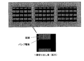
つぎに、チップを完全に切断する。このときのブレードの歯は、上述のハーフカットより狭いものを用いる。図14は、切断された状態のリードフレームパッケージを例示している。リードフレーム端面(側面電極)と、おもて面の配線の間は、未だ接続されていない。 Next, the chip is completely cut. The blade teeth used at this time are narrower than the half cut described above. FIG. 14 illustrates the lead frame package in a cut state. There is still no connection between the lead frame end face (side electrode) and the wiring on the front face.
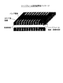
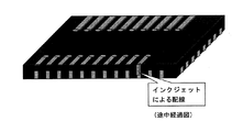
つぎに、図15に示すように、ナノ金属粒子、特に、ナノ銅金属粒子を用いたインクジェット方式により、必要な箇所の側面配線を行う。ナノ銅金属粒子を用いたインクジェット方式で形成した銅配線の有機溶媒による汚れや酸化物の除去についての詳細は、後述する。図15は、1個の配線のみが終了した途中経過図を示している。配線終了後、側面とおもて面にソルダーレジストを塗布する。そして、この段階で、バンプ形成部を開口して、バンプ電極を形成することもできる。 Next, as shown in FIG. 15, the side wiring of a required location is performed by the inkjet system using nano metal particles, especially nano copper metal particles. The details of removal of dirt and oxides by an organic solvent of a copper wiring formed by an inkjet method using nano copper metal particles will be described later. FIG. 15 shows an intermediate progress diagram in which only one wiring is completed. After wiring is complete, apply solder resist to the side and front surfaces. At this stage, the bump forming part can be opened to form a bump electrode.
図16は、本発明の両面電極パッケージを、有機基板型のものに適用した第3の例を示す斜視図及び断面図である。図16は、多層有機基板を用いたBGAタイプの両面電極パッケージを例示し、(A)はおもて面図を、(B)は下面図を、(C)は、ワイヤボンド接続方式について(A)中のラインA−A’で切断した断面図を、(D)は(C)と同様であるがフリップチップ接続方式の断面図を、それぞれ示している。なお、有機基板型両面電極パッケージにおいて、有機基板の上に位置する半導体チップ側をおもて面、その反対の有機基板側を下面と称している。 FIG. 16 is a perspective view and a sectional view showing a third example in which the double-sided electrode package of the present invention is applied to an organic substrate type. FIG. 16 exemplifies a BGA type double-sided electrode package using a multi-layer organic substrate, wherein (A) is a front view, (B) is a bottom view, and (C) is a wire bond connection method (A (D) is the same as (C), but shows a cross-sectional view of the flip chip connection method. In the organic substrate type double-sided electrode package, the semiconductor chip side positioned on the organic substrate is referred to as the front surface, and the opposite organic substrate side is referred to as the lower surface.
図16(C)のワイヤボンド接続方式の断面図に示されるように、LSIチップは、多層有機基板上に絶縁性のダイボンド材により接着されている(チップダイボンド)。1個のLSIチップを例示したが、複数のチップを積層することも可能である。 As shown in the cross-sectional view of the wire bond connection method in FIG. 16C, the LSI chip is bonded to the multilayer organic substrate with an insulating die bond material (chip die bond). Although one LSI chip has been illustrated, a plurality of chips can be stacked.
多層または単層有機基板は、単層や複数層から成る基板の各層に、それぞれ配線パターンを形成した後これらの基板を貼り合わせ、必要に応じて各層の配線パターンを接続するためのスルーホールを形成したものである。このスルーホールの内部には導体層が形成され、この導体層が下面側に形成された端面電極部であるランドと接続されている。即ち、スルーホールの導体層は、必ずしもそのままランドにはならない。さらに、このランドには、ハンダ材料を付着させて、外部接続用のバンプを形成することができる。このような多層または単層有機基板は、例えば、「ハンダボール」と呼ばれる小さいハンダ材料を丸めたもの(バンプ)を下面に実装した(BGA:Ball Grid Array)一括封止有機基板として公知である。 Multi-layer or single-layer organic substrates are formed with wiring patterns on each layer of single-layer or multiple-layer substrates, and then these substrates are bonded together, and through-holes for connecting the wiring patterns of each layer are formed as necessary. Formed. A conductor layer is formed inside the through hole, and the conductor layer is connected to a land which is an end face electrode portion formed on the lower surface side. That is, the through hole conductor layer is not necessarily a land as it is. Further, a solder material can be attached to the land to form a bump for external connection. Such a multi-layer or single-layer organic substrate is known as a packaged organic substrate (BGA: Ball Grid Array) in which a small solder material called a “solder ball” (bump) is mounted on the lower surface (BGA: Ball Grid Array). .
多層または単層有機基板の最上層の配線パターンに、ボンディングワイヤ接続電極となる金属パッド部が形成されると共に、該電極への配線が形成されている。この多層または単層有機基板の上面の金属パッド部と、LSIチップは、図10を参照して説明したリードフレーム型と同様に、Auワイヤーにより接続される(ワイヤボンド)。 In the uppermost wiring pattern of the multilayer or single layer organic substrate, a metal pad portion to be a bonding wire connection electrode is formed and wiring to the electrode is formed. The metal pad portion on the upper surface of the multilayer or single layer organic substrate and the LSI chip are connected by an Au wire (wire bond) in the same manner as the lead frame type described with reference to FIG.
或いは、図16(D)に示すように、LSIチップは、フリップチップ接続とすることも可能である。この場合、LSIチップは、多層または単層有機基板の最上層の配線パターンを通して接続される。 Alternatively, as shown in FIG. 16D, the LSI chip can be flip-chip connected. In this case, the LSI chip is connected through the wiring pattern on the uppermost layer of the multilayer or single layer organic substrate.
そして、図16(C)或いは(D)に示す構成において、多層有機基板の最外側位置で、側面電極が、多層または単層有機基板の最上層に形成されている金属パッド部に接続される。側面電極は、スタッドバンプ又はボールボンドにより形成することができる。従来より、半導体チップの電極に突起状のバンプ(スタッドバンプ)を形成し、このバンプを実装基板に形成された電極に直接接合する技術が知られている。本発明は、このようなそれ自体公知の技術を用いて、スタッドバンプを側面電極として形成することができる。或いは、それ自体公知の技術のように、例えば、金等のワイヤーの先端を加熱溶融してボールを形成した後、金属パッド部にそのボールを超音波併用熱圧着し、その後、ワイヤーを切断することによって側面電極として装着する。これらの側面電極の配置はウエハレベル半導体と同じように有機基板の切断領域にはみ出させ、切断時にその切断面が露出する位置に配置する。 In the configuration shown in FIG. 16C or 16D, the side electrode is connected to the metal pad portion formed on the uppermost layer of the multilayer or single-layer organic substrate at the outermost position of the multilayer organic substrate. . The side electrodes can be formed by stud bumps or ball bonds. 2. Description of the Related Art Conventionally, a technique is known in which bumps (stud bumps) are formed on electrodes of a semiconductor chip, and the bumps are directly joined to electrodes formed on a mounting substrate. In the present invention, a stud bump can be formed as a side electrode using a technique known per se. Alternatively, as in a technique known per se, for example, the tip of a wire such as gold is heated and melted to form a ball, and then the ball is thermocompression-bonded to the metal pad portion with ultrasonic waves, and then the wire is cut. By attaching as side electrode. These side electrodes are arranged so as to protrude into the cutting region of the organic substrate in the same manner as the wafer level semiconductor, and are arranged at positions where the cut surfaces are exposed at the time of cutting.
側面電極接続後、図12を参照して説明したリードフレームの場合と同様に、外界からの応力、汚染から守るためにエポキシ樹脂により封止される。つぎに、図13を参照して説明したリードフレームの場合と同様に、モールドおもて面に配線とバンプ電極が形成される(バンプ電極の形成は後でもよい)。この配線は、インクジェット方式或いはスクリーン印刷により形成する。 After connecting the side electrodes, as in the case of the lead frame described with reference to FIG. 12, it is sealed with an epoxy resin in order to protect it from external stress and contamination. Next, as in the case of the lead frame described with reference to FIG. 13, wiring and bump electrodes are formed on the mold front surface (the bump electrodes may be formed later). This wiring is formed by an inkjet method or screen printing.
次に、チップを個片化するために切断する。なお、エポキシ樹脂による封止後、配線前にチップ個片化のためのハーフカット(凹状やV字カット)を行うこともできる。これによって、側面のハーフカット部(形成された溝内)に一部が迫出している構造にして、後の側面電極との配線接続が容易になる。 Next, it cut | disconnects in order to divide a chip into pieces. In addition, after sealing with an epoxy resin, a half cut (concave or V-shaped cut) for chip separation can be performed before wiring. As a result, a part of the side half-cut portion (in the formed groove) protrudes, and wiring connection with the subsequent side electrode is facilitated.
つぎに、チップを完全に切断した後、前述したリードフレームの場合と同様にして、ナノ金属粒子、特に、ナノ銅金属粒子を用いたインクジェット方式により、必要な箇所の側面配線を行う。配線終了後、側面とおもて面にソルダーレジストを塗布する。そして、この段階で、バンプ部を開口して、バンプ電極を形成することもできる。 Next, after the chip is completely cut, side wiring of necessary portions is performed by an ink jet method using nano metal particles, particularly nano copper metal particles, in the same manner as the lead frame described above. After wiring is complete, apply solder resist to the side and front surfaces. At this stage, bump electrodes can be opened to form bump electrodes.
図17は、本発明の両面電極パッケージを、イメージセンサーパッケージに適用した第4の例を示す斜視図及び側面図を示している。このようなイメージセンサーチップパッケージは、例えば、画像センサーLSI、赤外線センサーLSI、温度センサーLSI等用のパッケージである。 FIG. 17 shows a perspective view and a side view showing a fourth example in which the double-sided electrode package of the present invention is applied to an image sensor package. Such an image sensor chip package is, for example, a package for an image sensor LSI, an infrared sensor LSI, a temperature sensor LSI, or the like.
半導体(Si)基板の上面(図中の下側面)にはイメージセンサー形成面が形成される。イメージセンサー形成面とは、センサーを構成するCMOS回路素子或いはCCD等の受光素子と、それを制御する制御部が多層配線で形成され、その多層配線部内の所定の配線層が、側面電極に接続される。さらに、半導体基板の上面には、透明絶縁膜が形成される。この透明絶縁膜を通して外部からの光線が、イメージセンサー形成領域の受光素子領域に入射できるように構成されている。 An image sensor forming surface is formed on the upper surface (lower surface in the drawing) of the semiconductor (Si) substrate. The image sensor formation surface is a light receiving element such as a CMOS circuit element or CCD constituting the sensor, and a control unit for controlling the light receiving element is formed by a multilayer wiring, and a predetermined wiring layer in the multilayer wiring part is connected to the side electrode. Is done. Further, a transparent insulating film is formed on the upper surface of the semiconductor substrate. Light rays from the outside can enter the light receiving element region in the image sensor formation region through the transparent insulating film.
チップ裏面側の構成は、図1〜図8を参照して説明した第1の例と同様に構成することができる。即ち、Si基板の裏面側においては、裏面絶縁層を塗布する。この裏面絶縁層の上に、裏面再配線を実施する。この裏面再配線は、本発明の特徴とする側面配線を通して、上面側の多層配線部の所望箇所に接続される。この裏面再配線の上に、保護膜が塗布される。さらに、再配線上のバンプ形成部上の保護膜に開口を設け、ここに、バンプ電極を形成する。 The configuration on the back side of the chip can be configured similarly to the first example described with reference to FIGS. That is, the back surface insulating layer is applied on the back surface side of the Si substrate. Back surface rewiring is performed on the back surface insulating layer. The rear surface rewiring is connected to a desired portion of the multilayer wiring portion on the upper surface side through the side surface wiring characterizing the present invention. A protective film is applied on the back surface rewiring. Further, an opening is provided in the protective film on the bump forming portion on the rewiring, and a bump electrode is formed here.
本発明は、ナノ金属粒子を用いるものであるが、特に、ナノ銅金属粒子を用いたインクジェット方式で形成した場合の、銅配線の有機溶媒による汚れや酸化物は、室温以上200℃以下の低温で除去する。以下、これについて、説明する。 The present invention uses nano metal particles, and particularly when formed by an ink jet method using nano copper metal particles, stains and oxides due to the organic solvent of the copper wiring are at a low temperature of room temperature to 200 ° C. Remove with. This will be described below.
(1)インクジェット法で銅配線を形成する。 (1) A copper wiring is formed by an inkjet method.
有機溶媒中にナノ銅金属粒子が含有されており、それをプリンターで実用されているインクジェット法で所望のパターンを描く。その後、有機溶剤を蒸発させた熱処理が行われる。 Nano copper metal particles are contained in an organic solvent, and a desired pattern is drawn by an inkjet method that is practically used in a printer. Thereafter, heat treatment is performed by evaporating the organic solvent.
本発明は、このように形成された銅配線に対して、有機溶媒による汚れや酸化物を除去する。有機溶剤を蒸発させる熱処理を行った場合、銅の表面酸化によって酸化銅が形成されてしまうが、これも後の原子状水素処理によって除去ができる。或いは、本発明は、有機溶剤を蒸発させる熱処理を行わない場合にも適用できる。熱処理を行わない場合は、有機溶剤を含有した状態になるが、後に行う原子状水素処理によって有機溶媒の除去も可能となる。 The present invention removes dirt and oxides due to organic solvents from the copper wiring thus formed. When heat treatment for evaporating the organic solvent is performed, copper oxide is formed by copper surface oxidation, which can also be removed by subsequent atomic hydrogen treatment. Or this invention is applicable also when not performing the heat processing which evaporates an organic solvent. When the heat treatment is not performed, the organic solvent is contained, but the organic solvent can be removed by an atomic hydrogen treatment performed later.
(2)次に、銅配線洗浄装置中で原子状水素もしくはアンモニア分解種で銅酸化物および有機溶媒汚染物を除去する。 (2) Next, copper oxide and organic solvent contaminants are removed with atomic hydrogen or ammonia decomposition species in a copper wiring cleaning device.
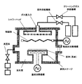
図18は、銅配線洗浄装置として用いた処理装置の断面の概略図である。反応室の上面のガス流入口からは、原子状水素もしくはアンモニア分解種の原料として、水素、アンモニア、ヒドラジン等の水素を含んだ原料を、クリーニングガス供給機構を通して送り込む。 FIG. 18 is a schematic view of a cross section of a processing apparatus used as a copper wiring cleaning apparatus. From the gas inlet on the upper surface of the reaction chamber, a raw material containing hydrogen, such as hydrogen, ammonia, hydrazine, or the like is fed as a raw material for atomic hydrogen or ammonia decomposition species through a cleaning gas supply mechanism.
反応室外の直下部にはヒータ等の基板加熱機構を設置し、この加熱機構直上の反応室内の試料ステージ上に、試料(基板)が、被着面を上に向けて設置される。ガス流入口からのガスを拡散させるシャワーヘッドと、試料の中間に、例えばタングステン線からなる触媒体を設置し、該触媒体を触媒体加熱機構により高温に加熱して流入したガスを分解する。これによって、原子状水素もしくはアンモニア分解種が、加熱触媒による接触分解反応により生成される。銅配線の酸化物は原子状水素の還元により取り除かれ、有機汚染物は原子状水素と炭素の反応により炭化水素が形成されることで除去できる。 A substrate heating mechanism such as a heater is installed immediately below the reaction chamber, and a sample (substrate) is placed on the sample stage in the reaction chamber immediately above the heating mechanism with the deposition surface facing upward. A catalyst body made of, for example, a tungsten wire is installed between the shower head for diffusing the gas from the gas inlet and the sample, and the catalyst body is heated to a high temperature by the catalyst body heating mechanism to decompose the inflowed gas. As a result, atomic hydrogen or ammonia decomposing species are generated by a catalytic decomposition reaction with a heating catalyst. Copper wiring oxides are removed by atomic hydrogen reduction, and organic contaminants can be removed by the formation of hydrocarbons by the reaction of atomic hydrogen and carbon.
原子状水素もしくはアンモニア分解種の原料である上述の水素を含む化合物として、窒素も含む化合物、例えば、アンモニア、ヒドラジンを用いることができる。この場合、該化合物気体を加熱された触媒体に接触させることにより原子状水素と同時に原子状窒素が発生し、原子状水素による金属表面酸化膜の還元、及び又は、有機物の除去とともに、原子状窒素により金属表面の窒化処理を行うことができる。 As the above-mentioned compound containing hydrogen which is a raw material of atomic hydrogen or ammonia decomposition species, a compound containing nitrogen, for example, ammonia or hydrazine can be used. In this case, by bringing the compound gas into contact with the heated catalyst body, atomic nitrogen is generated simultaneously with atomic hydrogen. At the same time as reduction of the metal surface oxide film by atomic hydrogen and / or removal of organic substances, The metal surface can be nitrided with nitrogen.
触媒体材料としては、上述のタングステン以外にも、タンタル、モリブデン、バナジウム、レニウム、白金、トリウム、ジルコニウム、イットリウム、ハフニウム、パラジウム、イリジウム、ルテニウム、鉄、ニッケル、クロム、アルミニウム、シリコン、炭素のいずれか1つの材料、これら材料の単体の酸化物、これら材料の単体の窒化物、これら材料(炭素を除く)の単体の炭化物、これらの材料から選択された2種類以上からなる混晶または化合物の酸化物、これらの材料から選択された2種類以上からなる混晶または化合物の窒化物、又は、これらの材料(炭素を除く)から選択された2種類以上からなる混晶または化合物の炭化物の何れか1つを用いることができる。また、触媒体の温度は、例えば、タングステン触媒体の場合は、1000℃から2200℃の温度範囲が適当である。 As the catalyst material, in addition to the above-mentioned tungsten, any of tantalum, molybdenum, vanadium, rhenium, platinum, thorium, zirconium, yttrium, hafnium, palladium, iridium, ruthenium, iron, nickel, chromium, aluminum, silicon, carbon Or a single oxide of these materials, a single nitride of these materials, a single carbide of these materials (excluding carbon), or a mixed crystal or compound of two or more selected from these materials Any of oxide, mixed crystal or compound nitride composed of two or more selected from these materials, or mixed crystal or compound carbide composed of two or more selected from these materials (excluding carbon) One can be used. The temperature of the catalyst body is, for example, a temperature range of 1000 ° C. to 2200 ° C. in the case of a tungsten catalyst body.
なお、図18中の原料供給機構は、必要に応じて、例えば、SiN系膜を堆積するために用いられるヘキサメチルジシラザンやシラン等を供給するためのものである。また、真空系は、反応残余ガスを排出するためのものである。 Note that the raw material supply mechanism in FIG. 18 is for supplying, for example, hexamethyldisilazane or silane used for depositing a SiN-based film as necessary. The vacuum system is for discharging reaction residual gas.
このような銅配線洗浄装置を用いて、試料(基板)として、ナノ銅金属粒子を用いたパターニング配線或いは側面配線を形成したウエハ、基板などを、試料ステージに設置する。そして、ナノ銅金属粒子を用いた配線による汚染を除去するため、水素ガスを流量30sccmで10分間流入し、この処理により、汚染の除去を行う。
Using such a copper wiring cleaning apparatus, as a sample (substrate), a wafer, a substrate, or the like on which patterning wiring or side wiring using nano copper metal particles is formed is placed on the sample stage. Then, in order to remove the contamination caused by the wiring using the nano copper metal particles, hydrogen gas is introduced at a flow rate of 30 sccm for 10 minutes, and this treatment removes the contamination.
Claims (8)
前記第1の配線部に接続される側面電極を形成し、
前記第2の配線部を、基板の上に形成した絶縁層の上に形成し、
個々の半導体パッケージに個片化するよう完全に切断した際に形成される前記第2の配線部の露出端と、前記側面電極をナノ金属粒子を用いてインクジェット方式により配線したことから成る半導体パッケージの製造方法。In a method for manufacturing a semiconductor package in which a first wiring part located on one side of a substrate and a second wiring part located on the other side are connected by wiring,
Forming a side electrode connected to the first wiring portion;
Forming the second wiring portion on an insulating layer formed on a substrate;
A semiconductor package comprising an exposed end of the second wiring portion formed when completely cut into individual semiconductor packages and the side electrodes wired by an ink jet method using nano metal particles Manufacturing method.
個々の半導体パッケージに個片化するよう完全に切断する際、スクライブラインにはみ出した側面電極も同時に切断することにより、パッケージ端面に側面電極を露出させて形成することから成る請求項1に記載の半導体パッケージの製造方法。The side electrode is formed at the same height as the post electrode connected to the first wiring part on one side of the substrate on which the LSI formation surface and the first wiring part are located, and is formed at the same time as the post electrode. And arranged so as to straddle both the chip end and the scribe line so as to be exposed when cut into individual chips from the wafer,
2. The method according to claim 1 , wherein when the semiconductor device is completely cut into individual semiconductor packages, the side electrodes protruding from the scribe line are simultaneously cut to expose the side electrodes on the package end surface. A method for manufacturing a semiconductor package.
前記第1の配線部は、前記有機基板の最上層に形成されている金属パッド部に接続される前記側面電極を含み、
前記有機基板の配線パターンと電気的接続した半導体チップの上を、一括モールドにより封止して前記絶縁層を形成し、かつ、該絶縁層上に前記第2の配線部を配線し、
個々の半導体パッケージに個片化するよう完全に切断した際に形成される前記第2の配線部の露出端と、前記側面電極との間を、インクジェット方式により配線したことから成る請求項1に記載の半導体パッケージの製造方法。The substrate comprises an organic substrate and a semiconductor chip bonded thereon,
The first wiring part includes the side electrode connected to a metal pad part formed in the uppermost layer of the organic substrate,
A semiconductor chip electrically connected to the wiring pattern of the organic substrate is sealed with a single mold to form the insulating layer, and the second wiring portion is wired on the insulating layer,
2. The wiring according to claim 1 , comprising wiring between an exposed end of the second wiring portion formed when the semiconductor package is completely cut into individual semiconductor packages and the side surface electrode by an ink jet method. The manufacturing method of the semiconductor package of description.
前記側面電極は、このハーフカット部に迫出した配線との間で配線したことから成る請求項5に記載の半導体パッケージの製造方法。After forming the insulating layer, half-cutting a batch mold part for chip separation, and wiring the second wiring part on the insulating layer including the half-cut part, Squeeze the material into a part of the side,
6. The method of manufacturing a semiconductor package according to claim 5 , wherein the side surface electrode is wired between the side electrode and the wiring protruding into the half cut portion.
前記第1の配線部は、リードフレームのインナーリード部及びアウターリード部を含み、該リードフレームのインナーリード部と電気的接続した半導体チップの上を、一括モールドにより封止して前記絶縁層を形成し、かつ、該絶縁層上に前記第2の配線部を配線し、
リードフレームを周囲の回路と電気的に接続するためのアウターリード部は、その先端断面が、リードフレーム裏面だけでなく、側面にも露出させて前記側面電極とし、
個々の半導体パッケージに個片化するよう完全に切断した際に形成される前記第2の配線部の露出端と、前記側面電極との間を、インクジェット方式により配線したことから成る請求項1に記載の半導体パッケージの製造方法。The substrate comprises a lead frame and a semiconductor chip bonded on the die pad,
The first wiring portion includes an inner lead portion and an outer lead portion of a lead frame, and the semiconductor layer electrically connected to the inner lead portion of the lead frame is sealed by batch molding to form the insulating layer. Forming and wiring the second wiring portion on the insulating layer,
The outer lead portion for electrically connecting the lead frame to the surrounding circuit has a cross-section at the tip thereof exposed not only on the back surface of the lead frame but also on the side surface to form the side electrode,
2. The wiring according to claim 1 , comprising wiring between an exposed end of the second wiring portion formed when the semiconductor package is completely cut into individual semiconductor packages and the side surface electrode by an ink jet method. The manufacturing method of the semiconductor package of description.
前記側面電極は、このハーフカット部に迫出した配線との間で配線したことから成る請求項7に記載の半導体パッケージの製造方法。After forming the insulating layer, half-cutting a batch mold part for chip separation, and wiring the second wiring part on the insulating layer including the half-cut part, Squeeze the material into a part of the side,
The method of manufacturing a semiconductor package according to claim 7 , wherein the side surface electrode is wired between the side electrode and the wiring protruding to the half cut portion.
Applications Claiming Priority (3)
| Application Number | Priority Date | Filing Date | Title |
|---|---|---|---|
| JP2005127266 | 2005-04-26 | ||
| JP2005127266 | 2005-04-26 | ||
| PCT/JP2006/307087 WO2006117961A1 (en) | 2005-04-26 | 2006-04-04 | Semiconductor package and method for manufacturing same |
Publications (2)
| Publication Number | Publication Date |
|---|---|
| JPWO2006117961A1 JPWO2006117961A1 (en) | 2008-12-18 |
| JP4635209B2 true JP4635209B2 (en) | 2011-02-23 |
Family
ID=37307767
Family Applications (1)
| Application Number | Title | Priority Date | Filing Date |
|---|---|---|---|
| JP2007514522A Expired - Fee Related JP4635209B2 (en) | 2005-04-26 | 2006-04-04 | Manufacturing method of semiconductor package |
Country Status (5)
| Country | Link |
|---|---|
| US (1) | US7838983B2 (en) |
| JP (1) | JP4635209B2 (en) |
| KR (1) | KR101189100B1 (en) |
| TW (1) | TW200703589A (en) |
| WO (1) | WO2006117961A1 (en) |
Families Citing this family (15)
| Publication number | Priority date | Publication date | Assignee | Title |
|---|---|---|---|---|
| US7939916B2 (en) * | 2007-01-25 | 2011-05-10 | Analog Devices, Inc. | Wafer level CSP packaging concept |
| US7843046B2 (en) * | 2008-02-19 | 2010-11-30 | Vertical Circuits, Inc. | Flat leadless packages and stacked leadless package assemblies |
| JP5033682B2 (en) * | 2008-03-12 | 2012-09-26 | 株式会社テラミクロス | SEMICONDUCTOR ELEMENT AND METHOD FOR MANUFACTURING SAME, SEMICONDUCTOR DEVICE AND METHOD FOR MANUFACTURING SAME |
| JP2009277970A (en) * | 2008-05-16 | 2009-11-26 | Fujikura Ltd | Circuit wiring board package |
| JP2009277969A (en) * | 2008-05-16 | 2009-11-26 | Fujikura Ltd | Semiconductor device and manufacturing method thereof, and semiconductor device laminate |
| JP5266009B2 (en) * | 2008-10-14 | 2013-08-21 | 株式会社フジクラ | Built-in circuit wiring board |
| CN101930929B (en) * | 2009-06-26 | 2012-07-18 | 日月光半导体(上海)股份有限公司 | Manufacturing method of packaging base plate provided with side surface lines |
| CN102804379B (en) * | 2010-05-24 | 2015-12-09 | 全视科技有限公司 | Double-sided image sensor |
| CN103155136B (en) | 2010-09-29 | 2015-03-04 | Nxp股份有限公司 | Singulation of IC packages |
| FR2967814A1 (en) * | 2010-11-23 | 2012-05-25 | St Microelectronics Grenoble 2 | Semiconductor device, has electrical connection of intermediate elements provided between support plate and chip and connected to electrical interconnection unit of plate and rear electrical interconnection network of chip |
| US9153507B2 (en) * | 2012-01-31 | 2015-10-06 | Broadcom Corporation | Semiconductor package with improved testability |
| JP2014120612A (en) * | 2012-12-17 | 2014-06-30 | Toshiba Corp | Semiconductor device, and semiconductor module using the same |
| JP6278251B2 (en) * | 2013-09-27 | 2018-02-14 | 富士電機株式会社 | Bonding assembly equipment |
| US9881962B2 (en) * | 2013-12-10 | 2018-01-30 | Sony Corporation | Semiconductor apparatus, solid state imaging device, imaging apparatus and electronic equipment, and manufacturing method thereof |
| US9972558B1 (en) | 2017-04-04 | 2018-05-15 | Stmicroelectronics, Inc. | Leadframe package with side solder ball contact and method of manufacturing |
Citations (3)
| Publication number | Priority date | Publication date | Assignee | Title |
|---|---|---|---|---|
| JP2004303884A (en) * | 2003-03-31 | 2004-10-28 | Seiko Epson Corp | Manufacturing method of three-dimensional mounting module and three-dimensional mounting module obtained by the method |
| JP2004342883A (en) * | 2003-05-16 | 2004-12-02 | Oki Electric Ind Co Ltd | Semiconductor device and method of manufacturing semiconductor device |
| JP2005005488A (en) * | 2003-06-12 | 2005-01-06 | Dainippon Printing Co Ltd | Semiconductor module and manufacturing method thereof |
Family Cites Families (7)
| Publication number | Priority date | Publication date | Assignee | Title |
|---|---|---|---|---|
| US5847930A (en) * | 1995-10-13 | 1998-12-08 | Hei, Inc. | Edge terminals for electronic circuit modules |
| JP3599950B2 (en) * | 1997-04-16 | 2004-12-08 | 株式会社アルバック | Method of firing metal paste |
| JP2002075999A (en) | 2000-08-31 | 2002-03-15 | Ulvac Japan Ltd | Method of forming copper wiring pattern |
| US7177137B2 (en) * | 2002-04-15 | 2007-02-13 | Avx Corporation | Plated terminations |
| JP3646719B2 (en) * | 2003-06-19 | 2005-05-11 | セイコーエプソン株式会社 | Semiconductor device and manufacturing method thereof, circuit board, and electronic apparatus |
| SG120123A1 (en) * | 2003-09-30 | 2006-03-28 | Micron Technology Inc | Castellated chip-scale packages and methods for fabricating the same |
| JP2005340647A (en) * | 2004-05-28 | 2005-12-08 | Nec Compound Semiconductor Devices Ltd | Interposer substrate, semiconductor package, semiconductor device, and manufacturing method thereof |
-
2006
- 2006-04-04 WO PCT/JP2006/307087 patent/WO2006117961A1/en not_active Ceased
- 2006-04-04 JP JP2007514522A patent/JP4635209B2/en not_active Expired - Fee Related
- 2006-04-04 KR KR1020077024617A patent/KR101189100B1/en not_active Expired - Fee Related
- 2006-04-04 US US11/911,990 patent/US7838983B2/en active Active
- 2006-04-24 TW TW095114554A patent/TW200703589A/en not_active IP Right Cessation
Patent Citations (3)
| Publication number | Priority date | Publication date | Assignee | Title |
|---|---|---|---|---|
| JP2004303884A (en) * | 2003-03-31 | 2004-10-28 | Seiko Epson Corp | Manufacturing method of three-dimensional mounting module and three-dimensional mounting module obtained by the method |
| JP2004342883A (en) * | 2003-05-16 | 2004-12-02 | Oki Electric Ind Co Ltd | Semiconductor device and method of manufacturing semiconductor device |
| JP2005005488A (en) * | 2003-06-12 | 2005-01-06 | Dainippon Printing Co Ltd | Semiconductor module and manufacturing method thereof |
Also Published As
| Publication number | Publication date |
|---|---|
| US7838983B2 (en) | 2010-11-23 |
| KR20080003832A (en) | 2008-01-08 |
| JPWO2006117961A1 (en) | 2008-12-18 |
| KR101189100B1 (en) | 2012-10-10 |
| WO2006117961A1 (en) | 2006-11-09 |
| US20090140364A1 (en) | 2009-06-04 |
| TW200703589A (en) | 2007-01-16 |
| TWI305034B (en) | 2009-01-01 |
Similar Documents
| Publication | Publication Date | Title |
|---|---|---|
| JP4635209B2 (en) | Manufacturing method of semiconductor package | |
| TWI229435B (en) | Manufacture of semiconductor device | |
| TWI429048B (en) | Method for manufacturing semiconductor carrier element and method of manufacturing semiconductor package using the same | |
| US8404516B2 (en) | Method for producing a MEMS package | |
| JP3942190B1 (en) | Semiconductor device having double-sided electrode structure and manufacturing method thereof | |
| US7399683B2 (en) | Manufacturing method of semiconductor device | |
| CN101771013A (en) | Semiconductor device and method of manufacturing the same | |
| WO2007018237A1 (en) | Semiconductor device and method for manufacturing same | |
| US10269583B2 (en) | Semiconductor die attachment with embedded stud bumps in attachment material | |
| JP4783906B2 (en) | Packaged stacked semiconductor device and manufacturing method thereof | |
| CN105938802B (en) | Resin-sealed semiconductor device and method of manufacturing the same | |
| JP2006210758A (en) | Semiconductor device having through electrode and method for manufacturing the same | |
| JP4215571B2 (en) | Manufacturing method of semiconductor device | |
| JP2005109427A (en) | Semiconductor device and manufacturing method thereof | |
| JP2003068738A (en) | Semiconductor device, method of manufacturing the same, semiconductor chip and method of mounting the same | |
| JP2012190939A (en) | Semiconductor device and manufacturing method of the same | |
| TW201737463A (en) | Semiconductor device and method of manufacturing same | |
| CN111344860A (en) | Die Attach Surface Copper Layer with Protective Layer for Microelectronic Devices | |
| JP2006202974A (en) | Electronic device and manufacturing method thereof | |
| JP6937283B2 (en) | Manufacturing method of semiconductor devices | |
| JP4483136B2 (en) | Semiconductor device mounting method and semiconductor device manufacturing method | |
| JP4286264B2 (en) | Semiconductor device and manufacturing method thereof | |
| JP4668608B2 (en) | Semiconductor chip, semiconductor device using the same, and semiconductor chip manufacturing method | |
| CN104051421A (en) | Semiconductor wafer structure combined with substrate through hole and metal bump and its manufacturing method | |
| JP2003031722A (en) | Semiconductor device and method of manufacturing the same |
Legal Events
| Date | Code | Title | Description |
|---|---|---|---|
| A131 | Notification of reasons for refusal |
Free format text: JAPANESE INTERMEDIATE CODE: A131 Effective date: 20100713 |
|
| A521 | Request for written amendment filed |
Free format text: JAPANESE INTERMEDIATE CODE: A523 Effective date: 20100723 |
|
| TRDD | Decision of grant or rejection written | ||
| A01 | Written decision to grant a patent or to grant a registration (utility model) |
Free format text: JAPANESE INTERMEDIATE CODE: A01 Effective date: 20101026 |
|
| A01 | Written decision to grant a patent or to grant a registration (utility model) |
Free format text: JAPANESE INTERMEDIATE CODE: A01 |
|
| R150 | Certificate of patent or registration of utility model |
Free format text: JAPANESE INTERMEDIATE CODE: R150 Ref document number: 4635209 Country of ref document: JP Free format text: JAPANESE INTERMEDIATE CODE: R150 |
|
| S111 | Request for change of ownership or part of ownership |
Free format text: JAPANESE INTERMEDIATE CODE: R313113 |
|
| R350 | Written notification of registration of transfer |
Free format text: JAPANESE INTERMEDIATE CODE: R350 |
|
| R250 | Receipt of annual fees |
Free format text: JAPANESE INTERMEDIATE CODE: R250 |
|
| R250 | Receipt of annual fees |
Free format text: JAPANESE INTERMEDIATE CODE: R250 |
|
| R250 | Receipt of annual fees |
Free format text: JAPANESE INTERMEDIATE CODE: R250 |
|
| R250 | Receipt of annual fees |
Free format text: JAPANESE INTERMEDIATE CODE: R250 |
|
| R250 | Receipt of annual fees |
Free format text: JAPANESE INTERMEDIATE CODE: R250 |
|
| R250 | Receipt of annual fees |
Free format text: JAPANESE INTERMEDIATE CODE: R250 |
|
| R250 | Receipt of annual fees |
Free format text: JAPANESE INTERMEDIATE CODE: R250 |
|
| R250 | Receipt of annual fees |
Free format text: JAPANESE INTERMEDIATE CODE: R250 |
|
| R250 | Receipt of annual fees |
Free format text: JAPANESE INTERMEDIATE CODE: R250 |
|
| LAPS | Cancellation because of no payment of annual fees |