JP4058633B2 - 面発光型発光素子、光モジュール、光伝達装置 - Google Patents
面発光型発光素子、光モジュール、光伝達装置 Download PDFInfo
- Publication number
- JP4058633B2 JP4058633B2 JP2003272890A JP2003272890A JP4058633B2 JP 4058633 B2 JP4058633 B2 JP 4058633B2 JP 2003272890 A JP2003272890 A JP 2003272890A JP 2003272890 A JP2003272890 A JP 2003272890A JP 4058633 B2 JP4058633 B2 JP 4058633B2
- Authority
- JP
- Japan
- Prior art keywords
- light
- electrode
- emitting element
- emitting
- light emitting
- Prior art date
- Legal status (The legal status is an assumption and is not a legal conclusion. Google has not performed a legal analysis and makes no representation as to the accuracy of the status listed.)
- Expired - Fee Related
Links
Images


Classifications
-
- H—ELECTRICITY
- H01—ELECTRIC ELEMENTS
- H01S—DEVICES USING THE PROCESS OF LIGHT AMPLIFICATION BY STIMULATED EMISSION OF RADIATION [LASER] TO AMPLIFY OR GENERATE LIGHT; DEVICES USING STIMULATED EMISSION OF ELECTROMAGNETIC RADIATION IN WAVE RANGES OTHER THAN OPTICAL
- H01S5/00—Semiconductor lasers
- H01S5/02—Structural details or components not essential to laser action
- H01S5/026—Monolithically integrated components, e.g. waveguides, monitoring photo-detectors, drivers
- H01S5/0262—Photo-diodes, e.g. transceiver devices, bidirectional devices
- H01S5/0264—Photo-diodes, e.g. transceiver devices, bidirectional devices for monitoring the laser-output
-
- H—ELECTRICITY
- H01—ELECTRIC ELEMENTS
- H01S—DEVICES USING THE PROCESS OF LIGHT AMPLIFICATION BY STIMULATED EMISSION OF RADIATION [LASER] TO AMPLIFY OR GENERATE LIGHT; DEVICES USING STIMULATED EMISSION OF ELECTROMAGNETIC RADIATION IN WAVE RANGES OTHER THAN OPTICAL
- H01S5/00—Semiconductor lasers
- H01S5/04—Processes or apparatus for excitation, e.g. pumping, e.g. by electron beams
- H01S5/042—Electrical excitation ; Circuits therefor
- H01S5/0425—Electrodes, e.g. characterised by the structure
- H01S5/04256—Electrodes, e.g. characterised by the structure characterised by the configuration
-
- H—ELECTRICITY
- H01—ELECTRIC ELEMENTS
- H01S—DEVICES USING THE PROCESS OF LIGHT AMPLIFICATION BY STIMULATED EMISSION OF RADIATION [LASER] TO AMPLIFY OR GENERATE LIGHT; DEVICES USING STIMULATED EMISSION OF ELECTROMAGNETIC RADIATION IN WAVE RANGES OTHER THAN OPTICAL
- H01S5/00—Semiconductor lasers
- H01S5/10—Construction or shape of the optical resonator, e.g. extended or external cavity, coupled cavities, bent-guide, varying width, thickness or composition of the active region
- H01S5/18—Surface-emitting [SE] lasers, e.g. having both horizontal and vertical cavities
- H01S5/183—Surface-emitting [SE] lasers, e.g. having both horizontal and vertical cavities having only vertical cavities, e.g. vertical cavity surface-emitting lasers [VCSEL]
- H01S5/18308—Surface-emitting [SE] lasers, e.g. having both horizontal and vertical cavities having only vertical cavities, e.g. vertical cavity surface-emitting lasers [VCSEL] having a special structure for lateral current or light confinement
- H01S5/18311—Surface-emitting [SE] lasers, e.g. having both horizontal and vertical cavities having only vertical cavities, e.g. vertical cavity surface-emitting lasers [VCSEL] having a special structure for lateral current or light confinement using selective oxidation
-
- H—ELECTRICITY
- H01—ELECTRIC ELEMENTS
- H01S—DEVICES USING THE PROCESS OF LIGHT AMPLIFICATION BY STIMULATED EMISSION OF RADIATION [LASER] TO AMPLIFY OR GENERATE LIGHT; DEVICES USING STIMULATED EMISSION OF ELECTROMAGNETIC RADIATION IN WAVE RANGES OTHER THAN OPTICAL
- H01S2301/00—Functional characteristics
- H01S2301/17—Semiconductor lasers comprising special layers
- H01S2301/176—Specific passivation layers on surfaces other than the emission facet
-
- H—ELECTRICITY
- H01—ELECTRIC ELEMENTS
- H01S—DEVICES USING THE PROCESS OF LIGHT AMPLIFICATION BY STIMULATED EMISSION OF RADIATION [LASER] TO AMPLIFY OR GENERATE LIGHT; DEVICES USING STIMULATED EMISSION OF ELECTROMAGNETIC RADIATION IN WAVE RANGES OTHER THAN OPTICAL
- H01S5/00—Semiconductor lasers
- H01S5/02—Structural details or components not essential to laser action
- H01S5/022—Mountings; Housings
- H01S5/02218—Material of the housings; Filling of the housings
- H01S5/02234—Resin-filled housings; the housings being made of resin
-
- H—ELECTRICITY
- H01—ELECTRIC ELEMENTS
- H01S—DEVICES USING THE PROCESS OF LIGHT AMPLIFICATION BY STIMULATED EMISSION OF RADIATION [LASER] TO AMPLIFY OR GENERATE LIGHT; DEVICES USING STIMULATED EMISSION OF ELECTROMAGNETIC RADIATION IN WAVE RANGES OTHER THAN OPTICAL
- H01S5/00—Semiconductor lasers
- H01S5/02—Structural details or components not essential to laser action
- H01S5/022—Mountings; Housings
- H01S5/0225—Out-coupling of light
- H01S5/02251—Out-coupling of light using optical fibres
-
- H—ELECTRICITY
- H01—ELECTRIC ELEMENTS
- H01S—DEVICES USING THE PROCESS OF LIGHT AMPLIFICATION BY STIMULATED EMISSION OF RADIATION [LASER] TO AMPLIFY OR GENERATE LIGHT; DEVICES USING STIMULATED EMISSION OF ELECTROMAGNETIC RADIATION IN WAVE RANGES OTHER THAN OPTICAL
- H01S5/00—Semiconductor lasers
- H01S5/02—Structural details or components not essential to laser action
- H01S5/022—Mountings; Housings
- H01S5/0235—Method for mounting laser chips
- H01S5/02355—Fixing laser chips on mounts
- H01S5/0237—Fixing laser chips on mounts by soldering
-
- H—ELECTRICITY
- H01—ELECTRIC ELEMENTS
- H01S—DEVICES USING THE PROCESS OF LIGHT AMPLIFICATION BY STIMULATED EMISSION OF RADIATION [LASER] TO AMPLIFY OR GENERATE LIGHT; DEVICES USING STIMULATED EMISSION OF ELECTROMAGNETIC RADIATION IN WAVE RANGES OTHER THAN OPTICAL
- H01S5/00—Semiconductor lasers
- H01S5/04—Processes or apparatus for excitation, e.g. pumping, e.g. by electron beams
- H01S5/042—Electrical excitation ; Circuits therefor
- H01S5/0425—Electrodes, e.g. characterised by the structure
- H01S5/04256—Electrodes, e.g. characterised by the structure characterised by the configuration
- H01S5/04257—Electrodes, e.g. characterised by the structure characterised by the configuration having positive and negative electrodes on the same side of the substrate
-
- H—ELECTRICITY
- H10—SEMICONDUCTOR DEVICES; ELECTRIC SOLID-STATE DEVICES NOT OTHERWISE PROVIDED FOR
- H10W—GENERIC PACKAGES, INTERCONNECTIONS, CONNECTORS OR OTHER CONSTRUCTIONAL DETAILS OF DEVICES COVERED BY CLASS H10
- H10W72/00—Interconnections or connectors in packages
- H10W72/50—Bond wires
- H10W72/531—Shapes of wire connectors
- H10W72/536—Shapes of wire connectors the connected ends being ball-shaped
-
- H—ELECTRICITY
- H10—SEMICONDUCTOR DEVICES; ELECTRIC SOLID-STATE DEVICES NOT OTHERWISE PROVIDED FOR
- H10W—GENERIC PACKAGES, INTERCONNECTIONS, CONNECTORS OR OTHER CONSTRUCTIONAL DETAILS OF DEVICES COVERED BY CLASS H10
- H10W72/00—Interconnections or connectors in packages
- H10W72/851—Dispositions of multiple connectors or interconnections
- H10W72/874—On different surfaces
- H10W72/884—Die-attach connectors and bond wires
-
- H—ELECTRICITY
- H10—SEMICONDUCTOR DEVICES; ELECTRIC SOLID-STATE DEVICES NOT OTHERWISE PROVIDED FOR
- H10W—GENERIC PACKAGES, INTERCONNECTIONS, CONNECTORS OR OTHER CONSTRUCTIONAL DETAILS OF DEVICES COVERED BY CLASS H10
- H10W74/00—Encapsulations, e.g. protective coatings
-
- H—ELECTRICITY
- H10—SEMICONDUCTOR DEVICES; ELECTRIC SOLID-STATE DEVICES NOT OTHERWISE PROVIDED FOR
- H10W—GENERIC PACKAGES, INTERCONNECTIONS, CONNECTORS OR OTHER CONSTRUCTIONAL DETAILS OF DEVICES COVERED BY CLASS H10
- H10W90/00—Package configurations
- H10W90/701—Package configurations characterised by the relative positions of pads or connectors relative to package parts
- H10W90/721—Package configurations characterised by the relative positions of pads or connectors relative to package parts of bump connectors
- H10W90/722—Package configurations characterised by the relative positions of pads or connectors relative to package parts of bump connectors between stacked chips
Landscapes
- Physics & Mathematics (AREA)
- Condensed Matter Physics & Semiconductors (AREA)
- General Physics & Mathematics (AREA)
- Electromagnetism (AREA)
- Optics & Photonics (AREA)
- Semiconductor Lasers (AREA)
Description
本発明の面発光型発光素子は、
半導体基板上に設けられ、該半導体基板と垂直に光を出射する発光素子部と、
前記発光素子部上に設けられた光検出部と、
前記光検出部を駆動させる第1電極および第2電極と、を含み、
前記光検出部は、
第2コンタクト層と、
前記第2コンタクト層の上方に設けられた光吸収層と、
前記光吸収層の上方に設けられた第1コンタクト層と、を含み、
前記第1コンタクト層は、
第1光通過部と、
前記第1光通過部から延出する少なくとも1つの第1電極接続部と、を含み、
前記第1電極は、前記第1コンタクト層のうち前記第1電極接続部上に設けられている。
本発明の光モジュールは、前記面発光型発光素子と、光導波路とを含む。また、本発明の光伝達装置は前記光モジュールを含む。
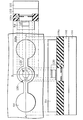
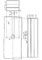
1.面発光型発光素子の構造
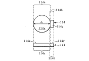
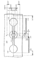
図1は、本発明を適用した第1の実施の形態に係る面発光型発光素子100を模式的に示す平面図および断面図である。図1においては、平面図と、この平面図のA−A線およびB−B線それぞれに沿った断面図とが示されている。また、図2は、図1に示す第1コンタクト層114を拡大して模式的に示す平面図および断面図である。図3は、図1に示す第2コンタクト層112を拡大して模式的に示す平面図および断面図である。図4は、図1に示す第1電極110、第2電極111、第3電極109および第4電極107を拡大して模式的に示す平面図および断面図である。なお、図2および図3では、第1コンタクト層114および第2コンタクト層112のみをそれぞれ抜き出して記載している。
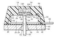
発光素子部140は、半導体基板(本実施形態ではn型GaAs基板)101上に設けられている。この発光素子部140は垂直共振器(以下「共振器」とする)からなり、柱状の半導体堆積体(以下「柱状部」とする)130を含む。
光検出部120は、第2コンタクト層112と、光吸収層113と、第1コンタクト層114とを含む。光吸収層113は第2コンタクト層112の上方に設けられ、第1コンタクト層114は光吸収層113の上方に設けられている。
本実施の形態の面発光型発光素子100においては、発光素子部140のn型第1ミラー102およびp型第2ミラー104、ならびに光検出部120のn型第1コンタクト層114およびp型第2コンタクト層112から、全体としてpnpn構造が構成される。なお、上記各層において、p型とn型を入れ替えることにより、全体としてnpnp構造を構成することもできる。
本実施の形態の面発光型発光素子100の一般的な動作を以下に示す。なお、下記の面発光型半導体レーザの駆動方法は一例であり、本発明の趣旨を逸脱しない限り、種々の変更が可能である。
次に、本発明を適用した第1の実施の形態の面発光型発光素子100の製造方法の一例について、図5〜図14を用いて説明する。図5〜図14は、図1に示す面発光型発光素子100の一製造工程を模式的に示す平面図および断面図であり、それぞれ図1に示す平面図および断面図に対応している。
本実施の形態の面発光型発光素子100は、以下に説明する作用効果1〜3を有する。なお、以下の各作用効果1〜3の説明の欄において、(A)にて、比較例である公知の面発光型発光素子の構造等を説明し、(B)にて、本実施の形態の面発光型発光素子100の構造および作用効果について説明する。
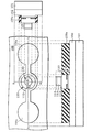
(A)公知の面発光型発光素子
図24は、公知の面発光型発光素子900を模式的に示す断面図および平面図である。この面発光型発光素子900は、半導体基板901上に設けられた発光素子部940と、発光素子部940上に設けられた光検出部920とを含む。発光素子部940は面発光型半導体レーザとして機能する。すなわち、発光素子部940において光(レーザ光)が生じる。光検出部920は前記光の一部を吸収し、吸収した光を光電流へと変換する。この光電流の値から、発光素子部940の光出力を検知することができる。
これに対して、本実施の形態の面発光型発光素子100によれば、図26(b)に示すように、第1コンタクト層114が第1光通過部114aと、第1光通過部114aから延出する第1電極接続部114bを含み、第1コンタクト層114のうち第1電極接続部114b上にのみ、第1電極110が設けられている。
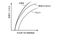
(A)面発光型半導体レーザは、駆動電流の大きさによって、発生するレーザ光の強度分布が変化する特性を有することが明らかになっている(IEEE Journal Of Quantum Electronics, Vol.38, No.2, February 2002)。面発光型半導体レーザにて発生するレーザ光がシングルモードである場合(図26(a)で一点破線で示した波形参照)、発生するレーザ光の強度分布の変化が小さいため、駆動電流の変化に対して、発生するレーザ光の強度分布の変化は比較的少ない。このため、図24に示す面発光型発光素子900において、発生するレーザ光がシングルモードである場合、第1コンタクト層914に入射した全光量に対する、出射面908から出射する光の割合は、駆動電流の変化によって著しく変化することはない。
(A)図24に示す面発光型発光素子900においては、第3電極909が発光素子部940上に設けられ、かつリング状の形状を有する。光検出部920は第3電極909の内側に設けられている。したがって、発光素子部940は光検出部920よりも直径が大きい。
1.面発光型発光素子の構造
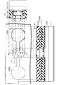
図15は、本発明を適用した第2の実施の形態に係る面発光型発光素子200を模式的に示す断面図である。図16は、図15に示す第2コンタクト層212を拡大して模式的に示す平面図および断面図である。図17は、図15に示す第2コンタクト層212および第2電極211を拡大して模式的に示す平面図および断面図である。なお、本実施の形態においては、第1の実施の形態と同様に、面発光型発光素子として面発光型半導体レーザを用いた場合について説明する。
本実施の形態の面発光型発光素子200の動作は、第1の実施の形態の面発光型発光素子100と基本的に同様であるため、詳しい説明は省略する。
本実施の形態に係る面発光型発光素子200の製造方法では、第2コンタクト層212をパターニングする工程で、所定の平面形状を有するレジスト層R6をマスクとしてパターニングすることにより、複数の第2電極接続部212bを設けた後(図18参照)、各第2電極接続部212b上に第2電極211を設ける。上記の点以外は、前述した第1の実施形態に係る面発光型発光素子100の製造工程(図5〜図14参照)と同様である。このため、詳しい説明は省略する。
本実施の形態に係る面発光型発光素子200は、第1の実施の形態に係る面発光型発光素子100と実質的に同じ作用および効果を有する。さらに、本実施の形態に係る面発光型発光素子200においては、第2コンタクト層212の第2電極接続部212bおよび第2電極211が複数設けられているため、第2コンタクト層212によって効果的に均一な電界を形成することができる。これにより、光検出部120をより高速に駆動させることができる。なお、本実施の形態の面発光型発光素子200の第2コンタクト層212および第2電極211を、後述する第3の実施の形態の面発光型発光素子に適用してもよい。
1.面発光型発光素子の構造
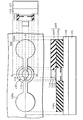
図19は、本発明を適用した第3の実施の形態に係る面発光型発光素子300を模式的に示す断面図である。なお、本実施の形態においては、第1および第2の実施の形態と同様に、面発光型発光素子として面発光型半導体レーザを用いた場合について説明する。
本実施の形態の面発光型発光素子300においては、光検出部320において、ダイオードの積層構造が第1の実施の形態の面発光型発光素子100と逆である。このため、本実施の形態の面発光型発光素子300の動作は、第1の実施の形態の面発光型発光素子100の動作と比較して、光検出部320において、光吸収層113にて光が吸収されることにより生じた電荷が移動する方向と、光電流が流れる方向とが反対である。上記の点以外の動作は、第1の実施の形態の面発光型発光素子100と基本的に同様であるため、詳しい説明は省略する。
本実施の形態に係る面発光型発光素子300の製造工程では、図20に示すように、第1コンタクト層114および光吸収層113をパターニングした後に、第2コンタクト層312を別途パターニングする工程を省略できる。また、第3電極109が第2電極の機能を兼ねるため、電極形成時に第2電極を形成する必要がない。上記の点以外は、前述した第1の実施形態に係る面発光型発光素子100の製造工程(図5〜図14参照)と同様である。このため、詳しい説明は省略する。
本実施の形態に係る面発光型発光素子300およびその製造方法は、第1の実施の形態に係る面発光型発光素子100およびその製造方法と実質的に同じ作用および効果を有する。
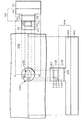
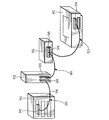
図21は、本発明を適用した第4の実施の形態の光モジュールを模式的に示す図である。この光モジュールは、第1の実施の形態の面発光型発光素子100(図1参照)と、半導体チップ20と、光ファイバ30とを含む。なお、本実施の形態の光モジュールにおいて、第1の実施の形態の面発光型発光素子100のかわりに、第2の実施の形態の面発光型発光素子200または第3の実施の形態の面発光型発光素子300を用いた場合でも、同様の作用および効果を奏することができる。このことは、後述する第5および第6の実施形態においても同様である。
面発光型発光素子100は、光ファイバ30の端面30aから出射される光を吸収する。この面発光型発光素子100は、光ファイバ30の端面30aとの相対的な位置が固定された状態となっている。具体的には、面発光型発光素子100の出射面108が光ファイバ30の端面30aと対向している。
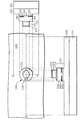
図22は、本発明を適用した第5の実施の形態の光伝達装置を示す図である。光伝達装置90は、コンピュータ、ディスプレイ、記憶装置、プリンタ等の電子機器92を相互に接続するものである。電子機器92は、情報通信機器であってもよい。光伝達装置90は、ケーブル94の両端にプラグ96が設けられたものであってもよい。ケーブル94は、光ファイバ30(図21参照)を含む。プラグ96は、面発光型発光素子100および半導体チップ20を内蔵する。なお、光ファイバ30はケーブル94に内蔵され、面発光型発光素子100および半導体チップ20はプラグ96に内蔵されているため、図22には図示されていない。光ファイバ30と面発光型発光素子100との取り付け状態は、第4の実施の形態にて説明した通りである。
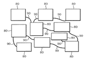
図23は、本発明を適用した第6の実施の形態の光伝達装置の使用形態を示す図である。光伝達装置90は、電子機器80間に接続されている。電子機器80として、液晶表示モニタまたはディジタル対応のCRT(金融、通信販売、医療、教育の分野で使用されることがある。)、液晶プロジェクタ、プラズマディスプレイパネル(PDP)、ディジタルTV、小売店のレジ(POS(Point of Sale Scanning)用)、ビデオ、チューナー、ゲーム装置、プリンタ等が挙げられる。
22 電極、 26 ハンダ、 28,46 穴、 29 テーパ、 30 光ファイバ、 30a 光ファイバの端面、 40 アンダーフィル材、 42 基板、 43 絶縁膜、 44 接着剤、 50 外部端子、 52 ワイヤ、 54 充填材、 56 樹脂、 80,92 電子機器、 90 光伝達装置、 94 ケーブル、 96 プラグ、 100,200,300 面発光型発光素子、 101 半導体基板、 101a 半導体基板101の表面、 101b 半導体基板101の裏面、 102 第1ミラー、 103 活性層、 104 第2ミラー、 104a 第2ミラー104の上面、 105 電流狭窄層、 106 絶縁層、 106a 第1絶縁層、 106b 第2絶縁層、 107 第4電極、 108 出射面、 109 第3電極、 110 第1電極、 111,211 第2電極、 112,212,312 第2コンタクト層、 112a,212a 第2光通過部、 112b,212b 第2電極接続部、 112x 第2光通過部112aの上面、 112y 第2電極接続部112bの上面、 113 光吸収層、 114,314 第1コンタクト層、 114a 第1光通過部、 114b 第1電極接続部、 114x 第1光通過部114aの上面、 114y 第1電極接続部114bの上面、 120,220,320 光検出部、 130 柱状部、 140 発光素子部、 150 半導体多層膜、 R1,R2,R3,R4,R5,R6,R7 レジスト層、 X,X1,X2 領域
Claims (13)
- 半導体基板上に設けられ、該半導体基板と垂直に光を出射する発光素子部と、
前記発光素子部上に設けられた光検出部と、
前記光検出部を駆動させる第1電極および第2電極と、を含み、
前記光検出部は、
第2コンタクト層と、
前記第2コンタクト層の上方に設けられた光吸収層と、
前記光吸収層の上方に設けられた第1コンタクト層と、を含み、
前記第1コンタクト層は、
第1光通過部と、
前記第1光通過部から部分的に突出する少なくとも1つの第1電極接続部と、を含み、
前記第1電極は、前記第1コンタクト層のうち前記第1電極接続部上に設けられている、面発光型発光素子。 - 請求項1において、
前記第1電極は、前記第1光通過部の上面から排除されている、面発光型発光素子。 - 請求項1または2において、
前記光検出部の上面は前記光の出射面を含み、
前記出射面の面積は前記第1光通過部の上面の面積とほぼ等しい、面発光型発光素子。 - 請求項3において、
前記出射面は前記第1光通過部の上面である、面発光型発光素子。 - 請求項1ないし4のいずれかにおいて、
前記第1電極および前記第2電極は前記光検出部を取り囲んでいない、面発光型発光素子。 - 請求項1ないし5のいずれかにおいて、
前記第2コンタクト層は、
第2光通過部と、
前記第2光通過部から部分的に突出する少なくとも1つの第2電極接続部と、を含み、
前記第2コンタクト層のうち前記第2電極接続部のみが、前記光検出部を駆動させるための第2電極とオーム性接触している、面発光型発光素子。 - 請求項1ないし6のいずれかにおいて、
前記発光素子部上にはさらに、前記発光素子部を駆動させるための第3電極の少なくとも一部が設けられ、
前記第3電極は、前記第2コンタクト層を部分的に取り囲むように設けられ、
前記第1光通過部は円柱状であり、
前記第3電極の内側面によって擬似円が構成され、
前記第1および第2電極は、前記第3電極によって部分的に取り囲まれた前記擬似円内の領域ならびに該領域の鉛直上方の領域内から排除されている、面発光型発光素子。 - 請求項7において、
前記擬似円の直径は、前記第1光通過部の断面の直径とほぼ等しい、面発光型発光素子。 - 請求項1ないし8のいずれかにおいて、
前記発光素子部は、面発光型半導体レーザとして機能する、面発光型発光素子。 - 請求項1ないし9のいずれかにおいて、
前記発光素子部および前記光検出部は、全体としてpnpn構造またはnpnp構造をなす、面発光型発光素子。 - 請求項1ないし9のいずれかにおいて、
前記発光素子部および前記光検出部は、全体としてnpn構造またはpnp構造をなす、面発光型発光素子。 - 請求項1ないし11のいずれかに記載の面発光型発光素子と、光導波路とを含む、光モジュール。
- 請求項12に記載の光モジュールを含む、光伝達装置。
Priority Applications (5)
| Application Number | Priority Date | Filing Date | Title |
|---|---|---|---|
| JP2003272890A JP4058633B2 (ja) | 2003-07-10 | 2003-07-10 | 面発光型発光素子、光モジュール、光伝達装置 |
| CNB2004100688145A CN100370660C (zh) | 2003-07-10 | 2004-07-05 | 表面发光型发光元件、光模块、光传输装置 |
| US10/886,654 US7339970B2 (en) | 2003-07-10 | 2004-07-09 | Surface light emitting element, optical module, light transmission device |
| EP04016263A EP1496582B1 (en) | 2003-07-10 | 2004-07-09 | Surface light emitting element, optical module, light transmission device |
| DE602004013682T DE602004013682D1 (de) | 2003-07-10 | 2004-07-09 | Oberflächenlichtemittierendes Bauelement, optisches Modul, Lichtübertragungsvorrichtung |
Applications Claiming Priority (1)
| Application Number | Priority Date | Filing Date | Title |
|---|---|---|---|
| JP2003272890A JP4058633B2 (ja) | 2003-07-10 | 2003-07-10 | 面発光型発光素子、光モジュール、光伝達装置 |
Publications (2)
| Publication Number | Publication Date |
|---|---|
| JP2005033106A JP2005033106A (ja) | 2005-02-03 |
| JP4058633B2 true JP4058633B2 (ja) | 2008-03-12 |
Family
ID=33448059
Family Applications (1)
| Application Number | Title | Priority Date | Filing Date |
|---|---|---|---|
| JP2003272890A Expired - Fee Related JP4058633B2 (ja) | 2003-07-10 | 2003-07-10 | 面発光型発光素子、光モジュール、光伝達装置 |
Country Status (5)
| Country | Link |
|---|---|
| US (1) | US7339970B2 (ja) |
| EP (1) | EP1496582B1 (ja) |
| JP (1) | JP4058633B2 (ja) |
| CN (1) | CN100370660C (ja) |
| DE (1) | DE602004013682D1 (ja) |
Families Citing this family (12)
| Publication number | Priority date | Publication date | Assignee | Title |
|---|---|---|---|---|
| US7408645B2 (en) * | 2003-11-10 | 2008-08-05 | Baker Hughes Incorporated | Method and apparatus for a downhole spectrometer based on tunable optical filters |
| JP3729271B2 (ja) | 2004-01-08 | 2005-12-21 | セイコーエプソン株式会社 | 光素子およびその製造方法 |
| JP2006339418A (ja) * | 2005-06-02 | 2006-12-14 | Seiko Epson Corp | 光素子及びその製造方法 |
| JP4449830B2 (ja) * | 2005-06-14 | 2010-04-14 | セイコーエプソン株式会社 | 面発光型半導体レーザ |
| JP4720637B2 (ja) * | 2005-09-07 | 2011-07-13 | セイコーエプソン株式会社 | 光素子及びその製造方法 |
| US20070081568A1 (en) * | 2005-10-06 | 2007-04-12 | Seiko Epson Corporation | Optical semiconductor element and method for manufacturing the same |
| JP2007173358A (ja) | 2005-12-20 | 2007-07-05 | Seiko Epson Corp | 光半導体素子及びその製造方法 |
| JP2007317686A (ja) | 2006-05-23 | 2007-12-06 | Seiko Epson Corp | 光素子チップ、並びに、光モジュールおよびその製造方法 |
| JP6015340B2 (ja) * | 2012-10-24 | 2016-10-26 | 富士ゼロックス株式会社 | 面発光型半導体レーザ、面発光型半導体レーザ装置、光伝送装置および情報処理装置 |
| JP6825251B2 (ja) * | 2016-07-12 | 2021-02-03 | 富士ゼロックス株式会社 | 発光素子 |
| JP6246879B1 (ja) * | 2016-09-20 | 2017-12-13 | 株式会社東芝 | 光半導体モジュール及びその製造方法 |
| EP4020724A4 (en) * | 2019-11-06 | 2023-09-13 | Sony Semiconductor Solutions Corporation | SURFACE EMITTING LASER DEVICE |
Family Cites Families (19)
| Publication number | Priority date | Publication date | Assignee | Title |
|---|---|---|---|---|
| DE69019498T2 (de) * | 1989-12-27 | 1996-02-29 | Nippon Electric Co | Optische Halbleitervorrichtung. |
| JPH0669491A (ja) * | 1992-08-18 | 1994-03-11 | Fujitsu Ltd | 光送受信装置 |
| JP3099921B2 (ja) * | 1992-09-11 | 2000-10-16 | 株式会社東芝 | 受光素子付き面発光型半導体レーザ装置 |
| US5606572A (en) * | 1994-03-24 | 1997-02-25 | Vixel Corporation | Integration of laser with photodiode for feedback control |
| US6026108A (en) * | 1996-10-16 | 2000-02-15 | The Regents Of The University Of California | Vertical-cavity surface-emitting laser with an intracavity quantum-well optical absorber |
| KR100234340B1 (ko) | 1996-10-29 | 1999-12-15 | 윤종용 | 광출력장치 |
| FR2770691B1 (fr) * | 1997-11-06 | 1999-12-03 | Alsthom Cge Alcatel | Dispositif d'emission optique a composant integre comportant au moins une section laser et une section de modulation |
| DE19807783A1 (de) | 1998-02-18 | 1999-09-02 | Siemens Ag | Bauelement mit einem Lichtsender und einem Lichtempfänger |
| JP3606063B2 (ja) | 1998-09-21 | 2005-01-05 | セイコーエプソン株式会社 | 面発光型半導体レーザの製造方法 |
| US6222202B1 (en) * | 1998-10-06 | 2001-04-24 | Agilent Technologies, Inc. | System and method for the monolithic integration of a light emitting device and a photodetector for low bias voltage operation |
| US6483862B1 (en) * | 1998-12-11 | 2002-11-19 | Agilent Technologies, Inc. | System and method for the monolithic integration of a light emitting device and a photodetector using a native oxide semiconductor layer |
| JP3928295B2 (ja) * | 1999-03-16 | 2007-06-13 | 富士ゼロックス株式会社 | 面発光型半導体レーザ |
| GB2349740A (en) | 1999-05-05 | 2000-11-08 | Mitel Semiconductor Ab | Vertical cavity surface emitting laser with monitoring diode |
| JP2001066299A (ja) | 1999-08-27 | 2001-03-16 | Toto Ltd | 検出装置および尿分析装置 |
| KR100317576B1 (ko) * | 1999-11-08 | 2001-12-24 | 윤덕용 | 모니터용 광검출기 일체형 표면광 레이저장치 |
| JP2001284723A (ja) * | 2000-03-30 | 2001-10-12 | Seiko Epson Corp | 面発光レーザおよびこれを用いた光送信モジュール |
| JP2001284725A (ja) | 2000-03-31 | 2001-10-12 | Seiko Epson Corp | 面発光型半導体レーザおよびその製造方法 |
| WO2003017372A1 (de) * | 2001-08-14 | 2003-02-27 | Infineon Technologies Ag | Photodiodenanordnung mit zwei photodioden |
| US20040071181A1 (en) * | 2002-10-15 | 2004-04-15 | Rong Huang | Retro-reflective etalon and the devices using the same |
-
2003
- 2003-07-10 JP JP2003272890A patent/JP4058633B2/ja not_active Expired - Fee Related
-
2004
- 2004-07-05 CN CNB2004100688145A patent/CN100370660C/zh not_active Expired - Fee Related
- 2004-07-09 DE DE602004013682T patent/DE602004013682D1/de not_active Expired - Lifetime
- 2004-07-09 US US10/886,654 patent/US7339970B2/en not_active Expired - Fee Related
- 2004-07-09 EP EP04016263A patent/EP1496582B1/en not_active Expired - Lifetime
Also Published As
| Publication number | Publication date |
|---|---|
| EP1496582A1 (en) | 2005-01-12 |
| EP1496582B1 (en) | 2008-05-14 |
| US20050056773A1 (en) | 2005-03-17 |
| JP2005033106A (ja) | 2005-02-03 |
| DE602004013682D1 (de) | 2008-06-26 |
| CN100370660C (zh) | 2008-02-20 |
| CN1578030A (zh) | 2005-02-09 |
| US7339970B2 (en) | 2008-03-04 |
Similar Documents
| Publication | Publication Date | Title |
|---|---|---|
| US7116854B2 (en) | Optical element array, optical module, and optical transmission device | |
| JP4815812B2 (ja) | 垂直共振器型面発光半導体レーザ装置 | |
| JP4058633B2 (ja) | 面発光型発光素子、光モジュール、光伝達装置 | |
| KR100631359B1 (ko) | 면발광형 반도체 레이저, 광 모듈 및 광 전달 장치 | |
| US20180048125A1 (en) | Light emitting element array and optical transmission device | |
| JP4092570B2 (ja) | 光素子およびその製造方法、光モジュール、ならびに光モジュールの駆動方法 | |
| US20070133642A1 (en) | Vertical cavity surface emitting laser module having monitoring photodiode and method of fabricating the same | |
| JP4386191B2 (ja) | 光素子 | |
| JP3719441B2 (ja) | 光素子およびその製造方法、光モジュール、光伝達装置 | |
| JP4892941B2 (ja) | 面発光型半導体レーザ装置およびその製造方法 | |
| JP2005166870A (ja) | 光素子及びその製造方法、光モジュール、光伝送装置 | |
| JP3846596B2 (ja) | 面発光型半導体レーザ、光モジュール、ならびに光伝達装置 | |
| JP2007329193A (ja) | 面発光型半導体レーザ装置およびその製造方法 | |
| JP4720637B2 (ja) | 光素子及びその製造方法 | |
| JP4946029B2 (ja) | 面発光型半導体レーザ | |
| JP2005019599A (ja) | 光素子およびその製造方法、光モジュール、光伝達装置 | |
| JP4356677B2 (ja) | 光半導体素子 | |
| JP3818391B2 (ja) | 光素子 | |
| JP3824089B2 (ja) | 光素子の製造方法 | |
| JP2018049869A (ja) | 光モジュールおよび光モジュールシステム | |
| JP2008004746A (ja) | 光半導体素子及びその製造方法 | |
| JP2007173358A (ja) | 光半導体素子及びその製造方法 | |
| JP2007103768A (ja) | 光半導体素子及びその製造方法 |
Legal Events
| Date | Code | Title | Description |
|---|---|---|---|
| RD04 | Notification of resignation of power of attorney |
Free format text: JAPANESE INTERMEDIATE CODE: A7424 Effective date: 20051221 |
|
| A977 | Report on retrieval |
Free format text: JAPANESE INTERMEDIATE CODE: A971007 Effective date: 20070316 |
|
| A131 | Notification of reasons for refusal |
Free format text: JAPANESE INTERMEDIATE CODE: A131 Effective date: 20070711 |
|
| A521 | Request for written amendment filed |
Free format text: JAPANESE INTERMEDIATE CODE: A523 Effective date: 20070906 |
|
| TRDD | Decision of grant or rejection written | ||
| A01 | Written decision to grant a patent or to grant a registration (utility model) |
Free format text: JAPANESE INTERMEDIATE CODE: A01 Effective date: 20071121 |
|
| A61 | First payment of annual fees (during grant procedure) |
Free format text: JAPANESE INTERMEDIATE CODE: A61 Effective date: 20071204 |
|
| FPAY | Renewal fee payment (event date is renewal date of database) |
Free format text: PAYMENT UNTIL: 20101228 Year of fee payment: 3 |
|
| R150 | Certificate of patent or registration of utility model |
Ref document number: 4058633 Country of ref document: JP Free format text: JAPANESE INTERMEDIATE CODE: R150 Free format text: JAPANESE INTERMEDIATE CODE: R150 |
|
| FPAY | Renewal fee payment (event date is renewal date of database) |
Free format text: PAYMENT UNTIL: 20101228 Year of fee payment: 3 |
|
| FPAY | Renewal fee payment (event date is renewal date of database) |
Free format text: PAYMENT UNTIL: 20111228 Year of fee payment: 4 |
|
| FPAY | Renewal fee payment (event date is renewal date of database) |
Free format text: PAYMENT UNTIL: 20111228 Year of fee payment: 4 |
|
| FPAY | Renewal fee payment (event date is renewal date of database) |
Free format text: PAYMENT UNTIL: 20121228 Year of fee payment: 5 |
|
| FPAY | Renewal fee payment (event date is renewal date of database) |
Free format text: PAYMENT UNTIL: 20121228 Year of fee payment: 5 |
|
| FPAY | Renewal fee payment (event date is renewal date of database) |
Free format text: PAYMENT UNTIL: 20131228 Year of fee payment: 6 |
|
| S531 | Written request for registration of change of domicile |
Free format text: JAPANESE INTERMEDIATE CODE: R313531 |
|
| R350 | Written notification of registration of transfer |
Free format text: JAPANESE INTERMEDIATE CODE: R350 |
|
| LAPS | Cancellation because of no payment of annual fees |