EP1496582B1 - Surface light emitting element, optical module, light transmission device - Google Patents
Surface light emitting element, optical module, light transmission device Download PDFInfo
- Publication number
- EP1496582B1 EP1496582B1 EP04016263A EP04016263A EP1496582B1 EP 1496582 B1 EP1496582 B1 EP 1496582B1 EP 04016263 A EP04016263 A EP 04016263A EP 04016263 A EP04016263 A EP 04016263A EP 1496582 B1 EP1496582 B1 EP 1496582B1
- Authority
- EP
- European Patent Office
- Prior art keywords
- electrode
- light
- light emitting
- contact layer
- layer
- Prior art date
- Legal status (The legal status is an assumption and is not a legal conclusion. Google has not performed a legal analysis and makes no representation as to the accuracy of the status listed.)
- Expired - Fee Related
Links
Images


Classifications
-
- H—ELECTRICITY
- H01—ELECTRIC ELEMENTS
- H01S—DEVICES USING THE PROCESS OF LIGHT AMPLIFICATION BY STIMULATED EMISSION OF RADIATION [LASER] TO AMPLIFY OR GENERATE LIGHT; DEVICES USING STIMULATED EMISSION OF ELECTROMAGNETIC RADIATION IN WAVE RANGES OTHER THAN OPTICAL
- H01S5/00—Semiconductor lasers
- H01S5/02—Structural details or components not essential to laser action
- H01S5/026—Monolithically integrated components, e.g. waveguides, monitoring photo-detectors, drivers
- H01S5/0262—Photo-diodes, e.g. transceiver devices, bidirectional devices
- H01S5/0264—Photo-diodes, e.g. transceiver devices, bidirectional devices for monitoring the laser-output
-
- H—ELECTRICITY
- H01—ELECTRIC ELEMENTS
- H01S—DEVICES USING THE PROCESS OF LIGHT AMPLIFICATION BY STIMULATED EMISSION OF RADIATION [LASER] TO AMPLIFY OR GENERATE LIGHT; DEVICES USING STIMULATED EMISSION OF ELECTROMAGNETIC RADIATION IN WAVE RANGES OTHER THAN OPTICAL
- H01S5/00—Semiconductor lasers
- H01S5/04—Processes or apparatus for excitation, e.g. pumping, e.g. by electron beams
- H01S5/042—Electrical excitation ; Circuits therefor
- H01S5/0425—Electrodes, e.g. characterised by the structure
- H01S5/04256—Electrodes, e.g. characterised by the structure characterised by the configuration
-
- H—ELECTRICITY
- H01—ELECTRIC ELEMENTS
- H01S—DEVICES USING THE PROCESS OF LIGHT AMPLIFICATION BY STIMULATED EMISSION OF RADIATION [LASER] TO AMPLIFY OR GENERATE LIGHT; DEVICES USING STIMULATED EMISSION OF ELECTROMAGNETIC RADIATION IN WAVE RANGES OTHER THAN OPTICAL
- H01S5/00—Semiconductor lasers
- H01S5/10—Construction or shape of the optical resonator, e.g. extended or external cavity, coupled cavities, bent-guide, varying width, thickness or composition of the active region
- H01S5/18—Surface-emitting [SE] lasers, e.g. having both horizontal and vertical cavities
- H01S5/183—Surface-emitting [SE] lasers, e.g. having both horizontal and vertical cavities having only vertical cavities, e.g. vertical cavity surface-emitting lasers [VCSEL]
- H01S5/18308—Surface-emitting [SE] lasers, e.g. having both horizontal and vertical cavities having only vertical cavities, e.g. vertical cavity surface-emitting lasers [VCSEL] having a special structure for lateral current or light confinement
- H01S5/18311—Surface-emitting [SE] lasers, e.g. having both horizontal and vertical cavities having only vertical cavities, e.g. vertical cavity surface-emitting lasers [VCSEL] having a special structure for lateral current or light confinement using selective oxidation
-
- H—ELECTRICITY
- H01—ELECTRIC ELEMENTS
- H01L—SEMICONDUCTOR DEVICES NOT COVERED BY CLASS H10
- H01L2224/00—Indexing scheme for arrangements for connecting or disconnecting semiconductor or solid-state bodies and methods related thereto as covered by H01L24/00
- H01L2224/01—Means for bonding being attached to, or being formed on, the surface to be connected, e.g. chip-to-package, die-attach, "first-level" interconnects; Manufacturing methods related thereto
- H01L2224/10—Bump connectors; Manufacturing methods related thereto
- H01L2224/15—Structure, shape, material or disposition of the bump connectors after the connecting process
- H01L2224/16—Structure, shape, material or disposition of the bump connectors after the connecting process of an individual bump connector
- H01L2224/161—Disposition
- H01L2224/16135—Disposition the bump connector connecting between different semiconductor or solid-state bodies, i.e. chip-to-chip
- H01L2224/16145—Disposition the bump connector connecting between different semiconductor or solid-state bodies, i.e. chip-to-chip the bodies being stacked
-
- H—ELECTRICITY
- H01—ELECTRIC ELEMENTS
- H01L—SEMICONDUCTOR DEVICES NOT COVERED BY CLASS H10
- H01L2224/00—Indexing scheme for arrangements for connecting or disconnecting semiconductor or solid-state bodies and methods related thereto as covered by H01L24/00
- H01L2224/01—Means for bonding being attached to, or being formed on, the surface to be connected, e.g. chip-to-package, die-attach, "first-level" interconnects; Manufacturing methods related thereto
- H01L2224/42—Wire connectors; Manufacturing methods related thereto
- H01L2224/47—Structure, shape, material or disposition of the wire connectors after the connecting process
- H01L2224/48—Structure, shape, material or disposition of the wire connectors after the connecting process of an individual wire connector
- H01L2224/4805—Shape
- H01L2224/4809—Loop shape
- H01L2224/48091—Arched
-
- H—ELECTRICITY
- H01—ELECTRIC ELEMENTS
- H01L—SEMICONDUCTOR DEVICES NOT COVERED BY CLASS H10
- H01L2224/00—Indexing scheme for arrangements for connecting or disconnecting semiconductor or solid-state bodies and methods related thereto as covered by H01L24/00
- H01L2224/01—Means for bonding being attached to, or being formed on, the surface to be connected, e.g. chip-to-package, die-attach, "first-level" interconnects; Manufacturing methods related thereto
- H01L2224/42—Wire connectors; Manufacturing methods related thereto
- H01L2224/47—Structure, shape, material or disposition of the wire connectors after the connecting process
- H01L2224/48—Structure, shape, material or disposition of the wire connectors after the connecting process of an individual wire connector
- H01L2224/484—Connecting portions
- H01L2224/48463—Connecting portions the connecting portion on the bonding area of the semiconductor or solid-state body being a ball bond
- H01L2224/48464—Connecting portions the connecting portion on the bonding area of the semiconductor or solid-state body being a ball bond the other connecting portion not on the bonding area also being a ball bond, i.e. ball-to-ball
-
- H—ELECTRICITY
- H01—ELECTRIC ELEMENTS
- H01L—SEMICONDUCTOR DEVICES NOT COVERED BY CLASS H10
- H01L2224/00—Indexing scheme for arrangements for connecting or disconnecting semiconductor or solid-state bodies and methods related thereto as covered by H01L24/00
- H01L2224/73—Means for bonding being of different types provided for in two or more of groups H01L2224/10, H01L2224/18, H01L2224/26, H01L2224/34, H01L2224/42, H01L2224/50, H01L2224/63, H01L2224/71
- H01L2224/732—Location after the connecting process
- H01L2224/73251—Location after the connecting process on different surfaces
- H01L2224/73265—Layer and wire connectors
-
- H—ELECTRICITY
- H01—ELECTRIC ELEMENTS
- H01L—SEMICONDUCTOR DEVICES NOT COVERED BY CLASS H10
- H01L2924/00—Indexing scheme for arrangements or methods for connecting or disconnecting semiconductor or solid-state bodies as covered by H01L24/00
- H01L2924/15—Details of package parts other than the semiconductor or other solid state devices to be connected
- H01L2924/181—Encapsulation
-
- H—ELECTRICITY
- H01—ELECTRIC ELEMENTS
- H01S—DEVICES USING THE PROCESS OF LIGHT AMPLIFICATION BY STIMULATED EMISSION OF RADIATION [LASER] TO AMPLIFY OR GENERATE LIGHT; DEVICES USING STIMULATED EMISSION OF ELECTROMAGNETIC RADIATION IN WAVE RANGES OTHER THAN OPTICAL
- H01S2301/00—Functional characteristics
- H01S2301/17—Semiconductor lasers comprising special layers
- H01S2301/176—Specific passivation layers on surfaces other than the emission facet
-
- H—ELECTRICITY
- H01—ELECTRIC ELEMENTS
- H01S—DEVICES USING THE PROCESS OF LIGHT AMPLIFICATION BY STIMULATED EMISSION OF RADIATION [LASER] TO AMPLIFY OR GENERATE LIGHT; DEVICES USING STIMULATED EMISSION OF ELECTROMAGNETIC RADIATION IN WAVE RANGES OTHER THAN OPTICAL
- H01S5/00—Semiconductor lasers
- H01S5/02—Structural details or components not essential to laser action
- H01S5/022—Mountings; Housings
- H01S5/02218—Material of the housings; Filling of the housings
- H01S5/02234—Resin-filled housings; the housings being made of resin
-
- H—ELECTRICITY
- H01—ELECTRIC ELEMENTS
- H01S—DEVICES USING THE PROCESS OF LIGHT AMPLIFICATION BY STIMULATED EMISSION OF RADIATION [LASER] TO AMPLIFY OR GENERATE LIGHT; DEVICES USING STIMULATED EMISSION OF ELECTROMAGNETIC RADIATION IN WAVE RANGES OTHER THAN OPTICAL
- H01S5/00—Semiconductor lasers
- H01S5/02—Structural details or components not essential to laser action
- H01S5/022—Mountings; Housings
- H01S5/0225—Out-coupling of light
- H01S5/02251—Out-coupling of light using optical fibres
-
- H—ELECTRICITY
- H01—ELECTRIC ELEMENTS
- H01S—DEVICES USING THE PROCESS OF LIGHT AMPLIFICATION BY STIMULATED EMISSION OF RADIATION [LASER] TO AMPLIFY OR GENERATE LIGHT; DEVICES USING STIMULATED EMISSION OF ELECTROMAGNETIC RADIATION IN WAVE RANGES OTHER THAN OPTICAL
- H01S5/00—Semiconductor lasers
- H01S5/02—Structural details or components not essential to laser action
- H01S5/022—Mountings; Housings
- H01S5/0235—Method for mounting laser chips
- H01S5/02355—Fixing laser chips on mounts
- H01S5/0237—Fixing laser chips on mounts by soldering
-
- H—ELECTRICITY
- H01—ELECTRIC ELEMENTS
- H01S—DEVICES USING THE PROCESS OF LIGHT AMPLIFICATION BY STIMULATED EMISSION OF RADIATION [LASER] TO AMPLIFY OR GENERATE LIGHT; DEVICES USING STIMULATED EMISSION OF ELECTROMAGNETIC RADIATION IN WAVE RANGES OTHER THAN OPTICAL
- H01S5/00—Semiconductor lasers
- H01S5/04—Processes or apparatus for excitation, e.g. pumping, e.g. by electron beams
- H01S5/042—Electrical excitation ; Circuits therefor
- H01S5/0425—Electrodes, e.g. characterised by the structure
- H01S5/04256—Electrodes, e.g. characterised by the structure characterised by the configuration
- H01S5/04257—Electrodes, e.g. characterised by the structure characterised by the configuration having positive and negative electrodes on the same side of the substrate
Definitions
- the present invention relates to a surface light emitting element according to the preamble portion of patent claim 1, as well as an optical module and a light transmission device including such a surface light emitting element.
- a surface light emitting element according to the preamble portion of claim 1 is known from EP 0 840 380 A2 .
- SLES laser surface light emitting semiconductor laser
- SLE element surface light emitting element
- an optical module employing an SLES laser may be equipped with a function to detect a portion of light emitted from the SLES laser.
- it is known to monitor the light intensity by mounting the SLES laser on a photo diode, and reflecting a portion of the light emitted from the SLES laser on a light emitting window of a package, and entering the resultant reflected light into the photo diode ( JP-A-2000- 323791 ).
- the reflected light is influenced by the mounting accuracy between the SLES laser and the photo diode, and the shape and size of the package. For this reason, it is difficult to accurately detect only the light emitted from the SLES laser by this method. Furthermore, it is necessary to mount the SLES laser on the photo diode and to provide the light emitting window of the package in order to reflect the light emitted from the SLES laser, therefore, it is difficult to make the module smaller.
- EP 0 840 380 A2 discloses a surface light emitting element, comprising a light emitting part provided on a semiconductor substrate for emitting light perpendicularly to a surface of the semiconductor substrate; a light detecting part; provided on the light emitting part; and a first electrode and a second electrode for applying a voltage for driving the light detecting part, wherein the light detecting part includes a second contact layer; a light absorption layer, provided on the second contact layer; and a first contact layer, provided on the light absorption layer, the first contact layer including a light passage part and at least one first electrode coupling part extending from the light passage part, wherein the first electrode is provided on the first electrode coupling part of the first contact layer.
- the first contact layer comprises the first light passage part and the first electrode coupling part, extending from the first light passage part.
- the first electrode is provided on the first electrode coupling part of the first contact layer, therefore, most of the light, passed through the light absorption layer and entered into the first light passage part, can be emitted from the upper surface of the first light passage part. Thereby, the output of the emitted light can be accurately detected.
- FIG. 1 shows a plan view and cross-sectional views schematically illustrating an SLE element 100 according to a first embodiment of the present invention.
- FIG. 1 a plan view and cross-sectional views along the A-A line and the B-B line of the plan view are shown.
- FIG. 2 shows a plan view and a cross-sectional view schematically illustrating the first contact layer 114 shown in FIG. 1 enlarged.
- FIG. 3 shows a plan view and a cross-sectional view schematically illustrating the second contact layer 112 shown in FIG. 1 enlarged.
- FIG. 4 shows a plan view and cross-sectional views schematically illustrating a first electrode 110, a second electrode 111, a third electrode 109 and a fourth electrode 107 shown in FIG. 1 enlarged.
- FIG. 2 and FIG. 3 only the first contact layer 114 and the second contact layer 112 are excerpted for description.
- the SLE element 100 comprises a light emitting part 140 and a light detecting part 120, provided on the light emitting part 140.
- the embodiment shows a case where the light emitting part 140 functions as an SLES laser.
- the SLE element 100 can emit a laser beam from an emitting surface 108 vertically to a semiconductor substrate 101.
- the emitting surface 108 is provided on an upper surface (an upper surface 114x of a first light passage part 114a described later) of the light detecting part 120.
- the light emitting part 140 is provided on the semiconductor substrate (n-type GaAs substrate for the embodiment) 101.
- the light emitting part 140 comprises a vertical resonator (hereinafter, referred to as "resonator”), and includes a columnar semiconductor stacked layer (hereinafter, referred to as "columnar part”) 130.
- resonator vertical resonator
- columnar part columnar semiconductor stacked layer
- the light emitting part 140 comprises sequentially deposited: a distributed reflection type multi-layered mirror (hereinafter, referred to as "first mirror") 102, in which forty pairs of an n-type Al 0.9 Ga 0.1 As layer and an n-type Al 0.15 Ga 0.85 As layer are deposited such that the n-type Al 0.9 Ga 0.1 As layer and the n-type Al 0.15 Ga 0.85 As are alternately arranged; an active layer 103, formed of a GaAs well layer and an Al 0.3 Ga 0.7 As barrier layer and including a quantum well structure formed of three layers for the well layer; and a distributed reflection type multi-layered mirror (hereinafter, referred to as "second mirror") 104, in which twenty five pairs of a p-type Al 0.9 Ga 0.1 As layer and a p-type Al 0.15 Ga 0.85 As layer are deposited such that the p-type Al 0.9 Ga 0.1 As layer and the p-type Al 0.15 Ga 0.85 As layer are alternately arranged.
- first mirror distributed reflection type
- the second mirror 104 is, for example, formed to be a p-type by doping C
- the first mirror 102 is, for example, formed to be an n-type by doping Si. Therefore, a pin diode is formed by the p-type second mirror 104, the active layer 103, which is undoped, and the n-type first mirror 102.
- a portion of from the laser beam emitting side of the SLE element 100 to the middle part of the first mirror 102 in the light emitting part 140 is etched in a circular shape viewing from the laser beam emitting side to form the columnar part 130.
- the shape of the columnar part 130 in plan view is circular, however, any shape is possible.
- a current aperture 105 made of aluminum oxide is formed in a region in proximity of the active layer 103. More particularly a part of one layer of the second mirror 104 is the current aperture 105.
- the current aperture 105 is formed in a ring shape. That is, the current aperture 105 has a coaxial circular shape of its cross section when the current aperture 105 is cut in a plane parallel to a surface 101a of the semiconductor substrate 101 shown in FIG. 1 (actually, one layer of the 25 Al 0.9 Ga 0.1 As layers of second mirror 104 is Al 0.98 Ga 0.02 As layer that has an oxidized portion center portion surrounded by a ring-shaped non oxidized portion. The oxidized portion is current aperture 105).
- an insulating layer (first insulating layer 106a) is formed so as to cover the sides of the columnar part 130 and the upper surface of the first mirror 102. That is, the side wall of the columnar part 130 is surrounded by the first insulating layer 106a.
- the first insulating layer 106a can be made of polyimide resin, fluorocarbon resin, acrylic resin or epoxy resin, in particular, polyimide resin or fluorocarbon resin is preferable from the viewpoint of easiness of machining or the insulation.
- the light emitting part 140 is provided with the third electrode 109 and the fourth electrode 107.
- the third electrode 109 and the fourth electrode 107 are used to drive the light emitting part 140.
- At least a part of the third electrode 109 is provided on the light emitting part 140.
- the third electrode 109 is provided on the columnar part 130 and the first insulating layer 106a. As shown in FIG. 1 , the third electrode 109 is provided so as to partially surround the second contact layer 112. That is, the third electrode 109 does not completely surround the second contact layer 112.
- the fourth electrode 107 is provided on the region of the upper surface of the first mirror 102 where the first insulating layer 106a is not provided. The embodiment shows a case where the fourth electrode 107 is provided on the first mirror 102, however, the fourth electrode 107 may be provided on a back surface 101b of the semiconductor substrate 101. This applied likewise to the second embodiment and the third embodiment described later.
- the third electrode 109 is, for example, formed of stacked layers of Pt, Ti and Au.
- the fourth electrode 107 is, for example, formed of stacked layers of an alloy of Au and Ge, and Au. Current flows into the active layer 103 through the third electrode 109 and the fourth electrode 107.
- Materials to form the third electrode 109 and the fourth electrode 107 are not limited to the above-mentioned materials, but an alloy of Au and Zn can be used, for example.
- the light detecting part 120 comprises a second contact layer 112, a light absorption layer 113, and a first contact layer 114.
- the light absorption layer 113 is provided on the second contact layer 112, and the first contact layer 114 is provided on the light absorption layer 113.
- the second contact layer 112 is, for example, formed of an n-type GaAs layer
- the light absorption layer 113 is, for example, formed of a GaAs layer, which is undoped
- the first contact layer 114 for example, can be formed of a p-type GaAs layer.
- the second contact layer 112 is, for example, formed to be a p-type by doping C
- the first contact layer 114 is, for example, formed to be a n-type by doping Si. Accordingly, a pin diode is formed by the n-type second contact layer 112, the light absorption layer 113, which is undoped, and the p-type first contact layer 114.
- the first electrode 110 and the second electrode 111 are provided in the light detecting part 120.
- the first electrode 110 and the second electrode 111 are used to drive the light detecting part 120.
- the first electrode 110 and the second electrode 111 do not surround the light detecting part 120.
- the first electrode 110 can be formed of the same material as that of the third electrode 109
- the second electrode 111 can be formed of the same material as that of the fourth electrode 107.
- the first electrode 110 and the second electrode 111 are excluded from inside of a region X. That is, the first electrode 110 and the second electrode 111 are not provided in the region X.
- the region X is formed by a region X 1 , partially surrounded by the third electrode 109, and a region X 2 , vertically above the region X, (refer to FIG. 4 ).
- a region shown by dots is the region X.
- the first contact layer 114 includes a first light passage part 114a and at least one first electrode coupling part 114b.
- the first electrode coupling part 114b extends from the first light passage part 114a.
- the first electrode 110 is provided only on the first electrode coupling part 114b (on an upper surface 114y of the first electrode coupling part 114b) of the first contact layer 114. That is, only the first electrode coupling part 114b of the first contact layer 114 is in ohmic contact with the first electrode 110, which drives the light detecting part 120. Accordingly, the first electrode 110 is excluded from the upper surface 114x of the first light passage part 114a.
- the first light passage part 114a is of cylindrical shape. Furthermore, the third electrode 109 partially surrounds the periphery of the second contact layer 112, and a circular arc is configured by the inner side surface of the third electrode 109. A diameter d2 of the circle defined by the circular arc (refer to FIG. 4 ) is substantially equal to a diameter d1 (refer to FIG. 1 and FIG. 2 ) of the cross section of the first light passage part 114a.
- the second contact layer 112 includes a second light passage part 112a and at least one second electrode coupling part 112b.
- the second electrode coupling part 112b extends from the second light passage part 112a.
- the second electrode coupling part 112b is preferably provided in a position where the second electrode coupling part 112b does not overlap - in plan view - with the first electrode coupling part 114b of the first contact layer 114.
- the second electrode 111 is provided only on the second electrode coupling part 112b (on an upper surface 112y of the second electrode coupling part 112b) of the second contact layer 112. That is, the second electrode 111 is excluded from an upper surface 112x of the second light passage part 112a. Furthermore, only the second electrode coupling part 112b of the second contact layer 112 is in ohmic contact with the second electrode 111, which drives the light detecting part 120.
- the area of the cross section and the position of the second light passage part 112a are preferably adjusted so that as much light as possible of the light emitted from the light emitting part 140 (specifically, the upper surface 104a of the second mirror 104), can enter into the light detecting part 120. More preferably, the setting position and area of the cross section of the second light passage part 112a are adjusted so that most of the light, emitted from the upper surface 104a of the second mirror 104, can enter the second light passage part 112a.
- the upper surface of the light detecting part 120 includes the emitting surface 108 of the light.
- the upper surface 114x of the first light passage part 114a of the first contact layer 114 is the emitting surface 108.
- the area of the emitting surface 108 is substantially equal to that of the upper surface 114x of the first light passage part 114a.
- the first electrode 110 is formed on the first electrode coupling part 114b and a second insulating layer 106b, and the second insulating layer 106b is formed on the first insulating layer 106a.
- the side wall of the first electrode coupling part 114a of the first contact layer 114, a part of the side wall of the light absorption layer 113, and the side wall of the second electrode coupling part 112b of the second contact layer 112 contact with the second insulating layer 106b.
- the second insulating layer 106b for example, can be formed of silicone nitride, silicone oxide or silicon oxide nitride.
- An insulating layer 106 is formed of the first insulating layer 106a and the second insulating layer 106b.
- the embodiment shows a case where the insulating layer 106 is formed of the first insulating layer 106a and the second insulating layer 106b, however, the insulating layer 106 is not limited to a two-layer structure, but it may be formed by patterning one layer made of the same material, for example.
- a pnpn-structure as a whole is formed by the n-type first mirror 102 and the p-type second mirror 104 in the light emitting part 140, and the n-type first contact layer 114 and the p-type second contact layer 112 in the light detecting part 120.
- an npnp-structure as a whole may also be formed by exchanging the p-type and the n-type of each of these layers.
- the light detecting part 120 has a function to monitor the optical output generated in the light emitting part 140. Specifically, the light detecting part 120 converts the light generated in the light emitting part 140 into current. The optical output generated in the light emitting part 140 is computed based on the current value.
- the light detecting part 120 a portion of the light generated by the light emitting part 140 is absorbed by the light absorption layer 113, and light excitation is generated by the absorbed light and then electrons and holes are generated. Then, the electrons move to the second electrode 111, and the holes move to the first electrode 110, due to the electrical field applied from the outside of the element. As a result, in the light detecting part 120, current is generated in a direction from the second contact layer 112 to the first contact layer 114.
- the optical output from the light emitting part 140 is primarily determined by a bias voltage applied to the light emitting part 140.
- the optical output from the light emitting part 140 changes greatly depending on the ambient temperature of the light emitting part 140 and the age of the light emitting part 140. For this reason, it is necessary to maintain a predetermined optical output for the light emitting part 140 by adjusting the value of the current flowing in the light emitting part 140 by monitoring the optical output from the light emitting part 140 with the light detecting part 120 and adjusting the voltage value applied to the light emitting part 140 based on the current value generated in the light detecting part 120.
- a feedback control of the voltage applied to the light emitting part 140 in response to the optical output of the light emitting part 140 can be performed by using an external electronic circuit (not shown).
- the embodiment has explained with reference to a case where the SLE element 100 is an SLES laser, however, the present invention is also applicable to light emitting elements other than an SLES laser, such as a semiconductor light emitting diode. This applies likewise to the second embodiment and the third embodiment described later.
- the light that entered the second contact layer 112 enters the light absorption layer 113 next. Because a portion of the entered light is absorbed by the light absorption layer 113, light excitation is generated in the light absorption layer 113, and electrons and holes are generated. The electrons move to the second electrode 111, and the holes move to the first electrode 110 due to the electrical field applied from the outside of the element. As a result, in the light detecting part 120, a current (photo-electric current) is generated in a direction from the second contact layer 112 to the first contact layer 114. The optical output of the light emitting part 140 can be detected by measuring the value of this current.
- a current photo-electric current
- FIGs. 5 through 14 show plan views and cross sectional views schematically illustrating one manufacturing process of the SLE element 100 shown in FIG. 1 , and correspond to the plan view and cross sectional views shown in FIG. 1 .
- the SLE element 100 including the light emitting part 140 and the light detecting part 120 is obtained as shown in FIG. 1 .
- the SLE element 100 according to the first embodiment has effects 1 through 3, described below.
- effects 1 through 3 the structure of the known SLE element, which is used as a comparison example, will be described first under (A), and the structure and effects of the SLE element 100 according to the first embodiment will then be described under (B).
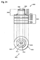
- FIG. 24 shows a plan view and a cross sectional view schematically illustrating a known SLE element 900.
- the SLE element 900 includes a light emitting part 940 provided on a semiconductor substrate 901, and a light detecting part 920 provided on the light emitting part 940.
- the light emitting part 940 functions as an SLES laser. That is, the light (laser beam) is emitted from the light emitting part 940.
- the light detecting part 920 absorbs a portion of the light and converts the absorbed light into electrical current, referred to as "photo-electric current" herein.
- the optical output of the light emitting part 940 can be detected from the photo-electric current value.
- the light emitting part 940 includes an n-type first mirror 902, an undoped active layer 903, and a p-type second mirror 904. These layers are provided on the n-type semiconductor substrate 901.
- the second mirror 904 is provided with a current aperture 905.
- a fourth electrode 907 is provided on a surface on the opposite side of the mounting surface of the first mirror 902 of the semiconductor substrate 901.
- a third electrode 909 is provided on the second mirror 904.
- a second electrode 911 is provided on a second contact layer 912.
- Each of the third electrode 909 and the second electrode 911 has a ring shape in plan view.
- the third electrode 909 and the fourth electrode 907 are provided to let current flow into the active layer 903.
- the first electrode 910 and the second electrode 911 are provided to drive the light detecting part 920.
- the light detecting part 920 is provided on the light emitting part 940 and includes a p-type second contact layer 912, an undoped light absorption layer 913, and an n-type first contact layer 914. Furthermore, the first electrode 910 is provided on the first contact layer 914. The first electrode 910 has a ring shape in plan view. In the light detecting part 920, the light absorbed in the light absorption layer 913 is converted into an photo-electric current.
- the emitting surface 908 of the SLE element 900 is provided on the upper surface of the light detecting part 920. Specifically, a bottom surface of an opening portion 990 formed by the first electrode 910 having a ring-shape is the emitting surface 908.
- the light emitting part 940 of the SLE element 900 will be described as generating a laser beam in multi-mode.
- FIG. 25 shows the relation between the driving current of the light emitting part 940, the output of light (optical output) emitted from the emitting surface 908, and the photo-electric current generated in the light detecting part 920 when the SLE element 900 is driven.
- the photo-electric current generated in the light detecting part 920 accurately detects the optical output from the light emitting part 940 (refer to the dotted line in FIG. 25 ).
- the SLE element 900 when a predetermined voltage is applied between the third electrode 909 and the fourth electrode 907, the driving current for the light emitting part 940 increases, and the photo-electric current is generated in the light detecting part 920 before the optical output is generated, that is, before light is emitted from the emitting surface 908. That is, in this case, it can be said that the optical output from the light emitting part 940 cannot be accurately detected by the value of the photo-electric current generated in the light detecting part 920.
- FIG. 26(a) shows a cross sectional view schematically illustrating in an enlarged manner a part of the light detecting part 920 of the SLE element 900 shown in FIG. 24 .
- FIG. 26(a) shows the light absorption layer 913, the first contact layer 914, and the first electrode 910 in the light detecting part 920. Additionally, FIG. 26(a) shows lines indicating the intensity distribution of a laser beam, generated in the active layer 903 in the light emitting part 940 and entering the light absorption layer 913; a dot-dash line shows the intensity distribution of the light in single-mode, and a solid line shows the intensity distribution of the light in multi-mode. In general, whether the laser beam generated from the SLES laser has single-mode or multi-mode depends on the diameter size of the current aperture.
- the first electrode 910 is provided on the first contact layer 914.
- the light, which passed through the light absorption layer 913 and entered the first contact layer 914 is reflected by the interface between the first electrode 910 and the first contact layer 914. Accordingly, in this region the light, which passed through the light absorption layer 913 and entered the first contact layer 914 is hardly emitted from the emitting surface 908.
- the relation between the driving current, the optical output and the photo-electric current shown in FIG. 25 corresponds to a case where a laser beam in multi-mode is generated in the light emitting part 940 of the SLE element 900. Accordingly, as shown in FIG. 26(a) , the photo-electric current is generated by the light, which entered a region of the first contact layer 914 located below the first electrode 910, therefore, it is considered that the photo-electric current, is generated before the optical output is generated.
- the first contact layer 114 comprises the first light passage part 114a and the first electrode coupling part 114b, extending from the first light passage part 114a, and the first electrode 110 is provided only on the first electrode coupling part 114b of the first contact layer 114.
- FIG. 26(b) shows a cross sectional view schematically illustrating in an enlarged manner a part of the light detecting part 120 of the SLE element 100 shown in FIG. 1 .
- the first electrode 110 is not provided on the first light passage part 114a. That is, the first electrode 110 is excluded from the upper surface 114x of the first light passage part 114a. According to this configuration, most of the light, which passed through the light absorption layer 113 and entered the first light passage part 114a, can be emitted from the upper surface 114x (emitting surface 108) of the first light passage part 114a.
- a correlation exists between the photo-electric current flowing in the light detecting part 120 and the output of the light emitted from the emitting surface 108. Accordingly, the output of the light emitted from the emitting surface 108 can be accurately detected.
- FIG. 15 shows a plan view and cross sectional views schematically illustrating an SLE element 200 according to a second embodiment of the present invention.
- FIG. 16 shows a plan view and a cross sectional view schematically illustrating a second contact layer 212 shown in FIG. 15 enlarged.
- FIG. 17 shows a plan view and a cross sectional view schematically illustrating a second contact layer 212 and a second electrode 211 shown in FIG. 15 enlarged.
- the second embodiment will be described with reference to a case where an SLES laser is used as the SLE element.
- the SLE element 200 according to the second embodiment generally has the same structure as the SLE element 100 according to the first embodiment except that a plurality of the second coupling parts 212b and second electrodes 211 are provided on the second contact layer 212.
- the structural elements, which are substantially the same as those in the SLE element 100 according to the first embodiment, are denoted by the same reference signs, and their detailed descriptions will be omitted.
- a plurality of the second coupling parts 212b of the second contact layer 212 are provided. Furthermore, the second electrodes 211 are provided on the second electrode coupling parts 212b. Furthermore, a part of the second electrode 211 is provided on the third electrode 109.
- the second electrode coupling parts 212b and the second electrodes 211 can be respectively made of the same materials as those of the first electrode coupling part 112b and the second electrode 111 of the first embodiment. As shown in FIG. 15 , each of the second electrode coupling parts 212 is provided at a position where each of the second electrode coupling parts 212b does not overlap - in plan view - with the first electrode coupling part 114b of the first contact layer 114.
- the operation of the SLE element 200 according to the second embodiment is basically the same as that of the SLE element 100 according to the first embodiment, therefore, the detailed description will be omitted.
- each of the second electrodes 211 is provided on each of the second electrode coupling parts 212b.
- the manufacturing process is same as that of the manufacturing process (refer to FIGs. 5 through 14 ) of the SLE element 100 according to the above-described first embodiment. Therefore, the detailed description will be omitted.
- the SLE element 200 according to the second embodiment has substantially the same effects as the SLE element 100 according to the first embodiment. Furthermore, in the second embodiment the plurality of the second electrode coupling parts 212b and the second electrodes 211 of the second contact layer 212 are provided and, therefore, a uniform electric field can be effectively formed by the second contact layer 212. This allows the light detecting part 120 to drive at a higher speed. In addition, the second contact layer 212 and the second electrode 211 of the SLE element 200 according to the second embodiment may be applied to an SLE element of the third embodiment described below.
- FIG. 19 shows a plan view and cross sectional views schematically illustrating an SLE element 300 according to a third embodiment.
- the third embodiment will be described with reference to a case where an SLES laser is used as the SLE element.
- the SLE element 300 according to the third embodiment has a different structure from the SLE element 100 according to the first embodiment in that a light detecting part 320 includes a second contact layer 312, formed of p-type GaAs, and a first contact layer 314, formed of n-type GaAs, the second electrode coupling part is not provided on the second contact layer 312, and the third electrode 109 also functions as a second electrode. Except for the above points, it has generally the same structure as the SLE element 100 according to the first embodiment. For this reason, the structural elements, which are substantially the same as those in the SLE element 100 according to the first embodiment, are denoted by the same reference signs, and their detailed descriptions will be omitted.
- the second contact layer 312 formed of p-type GaAs, the undoped light absorption layer 113, and the first contact layer 314, formed of n-type GaAs, are deposited in this order.
- the second contact layer 312, the light absorption layer 113, and the first contact layer 314 have the same shapes in plan view.
- the third electrode 109 in the light emitting part 140 also functions as the second electrode, which drives the light detecting part 320. That is, the light emitting part 140 and the light detecting part 320 share the third electrode 109.
- the n-type first mirror 102, the active layer 103, and the p-type second mirror 104 are deposited in this order. Furthermore, the p-type second contact layer 312 of the light detecting part 320 is provided on the p-type second mirror 104. Accordingly, the light emitting part 140 and the light detecting part 320 as a whole form an npn structure by the n-type first mirror 102, the p-type second mirror 104, the p-type second contact layer 312, and the n-type first contact layer 314. In this case, an SLE element having a pnp structure as a whole can be formed by exchanging the n-type and the p-type in each layer.
- the deposited structure of the diode is in reverse of that of the SLE element 100 according to the first embodiment.
- the moving direction of electric charges, generated by the absorption of the light in the light absorption layer 113 is opposite of the direction in that the photo-electric current flows.
- the operation except for the above point is basically the same as that of the SLE element 100 according to the first embodiment, therefore, the detailed description will be omitted.
- a process of separately patterning the second contact layer 312 after patterning the first contact layer 114 and the light absorption layer 113 can be omitted.
- the third electrode 109 also functions as the second electrode, therefore, it is unnecessary to form the second electrode when forming electrodes.
- the manufacturing process of the third embodiment is the same as the manufacturing process (refer to FIGs. 5 through 14 ) of the SLE element 100 according to the first embodiment described above. For this reason, the detailed description will be omitted.
- the SLE element 300 and the manufacturing method according to the third embodiment have substantially the same effects as the SLE element 100 and the manufacturing method according to the first embodiment.
- the process of separately patterning the second contact layer 312 is unnecessary, therefore, the SLE element 300 can be manufactured in a shorter process.
- the light emitting part 140 and the light detecting part 320 share the third electrode 109, therefore, it is unnecessary to separately form the second electrode, which drives the light detecting part 320. This allows the manufacturing process to be shortened.
- FIG. 21 shows a view schematically illustrating an optical module according to a fourth embodiment of the present invention.
- the optical module includes the SLE element 100 of the first embodiment (refer to FIG. 1 ), a semiconductor chip 20, and an optical fiber 30.
- An optical module achieving the same effects can be obtained even when the SLE element 200 according to the second embodiment or the SLE element 300 according to the third embodiment is used instead of the SLE element 100 according to the first embodiment. This applies likewise to the fifth embodiment and the sixth embodiment described later.
- the SLE element 100 absorbs the light emitted from an end face 30a of the optical fiber 30.
- the relative position of the SLE element 100 with the end face 30a of the optical fiber 30 is fixed.
- the emitting surface 108 of the SLE element 100 faces the end face 30a of the optical fiber 30.
- the semiconductor chip 20 is mounted to drive the SLE element 100. That is, the semiconductor chip 20 incorporates a circuit to drive the SLE element 100.
- a plurality of electrodes (or pads) 22, electrically coupled to the internal circuit, are formed on the semiconductor chip 20.
- Wiring patterns 24 and 64, electrically coupled to at least one of the electrodes 22, are preferably formed on a surface where the electrodes 22 are formed.
- the semiconductor chip 20 and the SLE element 100 are electrically coupled.
- a wiring pattern 14 and the wiring pattern 24 formed on the semiconductor chip 20 are electrically coupled via solder 26.
- the wiring pattern 14 is electrically coupled to the third electrode 109 (not shown in FIG. 21 ) of the SLE element 100.
- a wiring pattern 34 and the wiring pattern 64 formed on the semiconductor chips 20 are electrically coupled via the solder 26.
- the wiring pattern 34 is electrically coupled to the fourth electrode 107 (not shown in FIG. 21 ) of the SLE element 100.
- the SLE element 100 can be face-down mounted to the semiconductor chip 20. This allows not only electrical coupling by the solder 26, but also fixing the SLE element 100 and the semiconductor chip 20.
- a wire or conductive paste may be used for coupling the wiring pattern 14 and the wiring pattern 24, and the wiring patter 34 and the wiring pattern 64.
- Underfill material 40 may be provided between the SLE element 100 and the semiconductor chip 20.
- the underfill material 40 covers the emitting surface 108 of the SLE element 100, the underfill material 40 is transparent.
- the underfill material 40 covers and protects the electrical coupling between the SLE element 100 and the semiconductor chip 20, and further protects the surfaces of the SLE element 100 and the semiconductor chip 20. Furthermore, the underfill material 40 maintains a coupling state of the SLE element 100 and semiconductor chip 20.
- a hole portion 28 (for example, a through-hole portion) may be formed in the semiconductor chip 20.
- the optical fiber 30 is inserted into the hole portion 28.
- the hole portion 28 is formed from the surface where the electrode 22 is formed, and extends to the surface of the opposite side while avoiding the internal circuit.
- a taper 29 is preferably formed in at least one opening end of the hole portion 28. By forming the taper 29, the optical fiber 30 can be easily inserted into the hole portion 28.
- the semiconductor chip 20 may be mounted on a substrate 42. More specifically, the semiconductor chip 20 may be mounted on the substrate 42 via an adhesive agent 44.
- a hole portion 46 is formed in the substrate 42. The hole portion 46 is formed at a position where it communicates with the hole portion 28 in the semiconductor chip 20.
- the adhesive agent 44, adhering the semiconductor chip 20 and the substrate 42, is provided not to inhibit communication of the two hole portions 28 and 46, and not to block these hole portions.
- the hole portion 46 in the substrate 42 is tapered so that the inner diameter is larger in the direction opposite to the semiconductor chip 20. This allows easier insertion of the optical fiber 30.
- the substrate 42 may be formed of an insulating material such as resin, glass and ceramics, or may be formed of a conductive material such as metal.
- an insulating film 43 is preferably formed at least on the surface where the semiconductor chip 20 is mounted. Similar materials may be used for the substrate 42 in the following embodiments.
- the substrate 42 preferably has high heat conductivity. This facilitates the heat dissipation of the SLE element 100 and/or the semiconductor chip 20.
- the substrate 42 is a heat sink or a heat spreader.
- the semiconductor chip 20 is adhered to the substrate 42, therefore, the semiconductor chip 20 can be directly cooled.
- the adhesive agent 44, adhering the semiconductor chip 20 to the substrate 42, preferably has heat conductivity.
- the SLE element 100 coupled to the semiconductor chip 20 is also cooled.
- a wiring pattern 48 is provided on the substrate 42. Furthermore, an external terminal 50 is provided on the substrate 42. In this embodiment, the external terminal 50 is a lead wire.
- the wiring pattern 48 is electrically coupled to the electrodes 22 on the semiconductor chip 20, and at least one of wiring patterns 24 and 64 formed on the semiconductor chip 20 through a wire 52, for example. Furthermore, the wiring pattern 48 may be electrically coupled to the external terminal 50.
- the optical fiber 30 is inserted into the hole portion 28 in the semiconductor chip 20. Furthermore, the optical fiber 30 is also inserted into the hole portion 46 in the substrate 42.
- the internal diameter of the hole portion 46 becomes gradually smaller toward the hole portion 28 in the semiconductor chip 20, and on the surface that is opposite to the semiconductor chip 20, the internal diameter of the opening of the hole portion 46 becomes larger than the diameter of the optical fiber 30.
- the gap between the optical fiber 30 and the inside surface of the hole portion 46 is preferably filled with filling material 54 such as resin.
- the filling material 54 also has a function to fix the optical fiber 30 and to prevent it from being pulled out.
- the optical fiber 30 may be a single-mode fiber or a multi-mode fiber.
- the SLE element 100 emits multi-mode light
- the optical fiber 30 by using a multi-mode fiber as the optical fiber 30, the light emitted from the SLE element 100 can be reliably entered to the optical fiber 30.
- the SLE element 100 and the semiconductor chip 20 are sealed with resin 56.
- the resin 56 also seals the electrical coupling between the SLE element 100 and the semiconductor chip 20, and the electrical coupling between the semiconductor chip 20 and the wiring pattern 48, provided on the substrate 42.
- FIG. 22 shows a view explaining a light transmission device according to a fifth embodiment of the present invention.
- a light transmission device 90 mutually couples electronic devices 92 such as computer, display, storage device and printer.
- the electronic device 92 may be an information communication device.
- the light transmission device 90 may be a cable 94, whose both ends are provided with plugs 96.
- the cable 94 includes the optical fiber 30 (refer to FIG. 21 ).
- the plug 96 incorporates the SLE element 100 and the semiconductor chip 20.
- the optical fiber 30 is incorporated into the cable 94, and the SLE element 100 and the semiconductor chip 20 are incorporated into the plug 96, therefore, they are not shown in FIG. 22 .
- the mounting state of the optical fiber 30 and the SLE element 100 is the same as described in the fourth embodiment.
- One end of the optical fiber 30 is provided with the SLE element according to the first, second or third embodiment, and the other end of the optical fiber 30 is provided with a light receiving element (not shown).
- the light receiving element converts an inputted optical signal into an electrical signal, and then, inputs the electrical signal into one of the electronic devices 92.
- an electrical signal outputted from the electronic devices 92 is converted into an optical signal by the SLE element.
- the optical signal is transmitted through the optical fiber 30 and inputted into the light receiving element.
- information transmission between the electronic devices 92 can be performed by optical signals.
- FIG. 23 shows a view showing a usage configuration of a light transmission device according to a sixth embodiment of the present invention.
- the light transmission device 90 is coupled between electronic devices 80, such as a liquid crystal display monitor, a CRT adapted to digital technology (it may be used in fields of financing, mail-order, medical service and education), a liquid crystal projector, a plasma display panel (PDP), a digital TV, a cash register in retail shop (POS: Point of Sale Scanning), a video, a tuner, a game device, a printer and the like.
- electronic devices 80 such as a liquid crystal display monitor, a CRT adapted to digital technology (it may be used in fields of financing, mail-order, medical service and education), a liquid crystal projector, a plasma display panel (PDP), a digital TV, a cash register in retail shop (POS: Point of Sale Scanning), a video, a tuner, a game device, a printer and the like.
- the present invention is not limited to the above-described embodiments, but various modifications can be made.
- the present invention includes substantially same configurations (for example, a configuration of same functions, methods and results, and a configuration of same purposes and results) as described in the embodiments.
- the present invention includes configurations, in which non-essential parts of the configurations described in the embodiments are replaced.
- the present invention includes configurations, in which same effects are obtained and same objects are achieved as in the configurations described in the above embodiments.
- the present invention includes configurations, in which known arts are added to the configurations described in the embodiments.
- exchanging the p-type and the n-type in each semiconductor layer does not depart from the spirit of the present invention.
- configurations using AlGaAs have been described, however, other materials, for example, semiconductor materials such as GalnP. ZnSSe, InGaN, AlGaN, InGaAs, GalnNAs and GaAsSb can be used.
Landscapes
- Physics & Mathematics (AREA)
- Condensed Matter Physics & Semiconductors (AREA)
- General Physics & Mathematics (AREA)
- Electromagnetism (AREA)
- Optics & Photonics (AREA)
- Semiconductor Lasers (AREA)
Applications Claiming Priority (2)
| Application Number | Priority Date | Filing Date | Title |
|---|---|---|---|
| JP2003272890 | 2003-07-10 | ||
| JP2003272890A JP4058633B2 (ja) | 2003-07-10 | 2003-07-10 | 面発光型発光素子、光モジュール、光伝達装置 |
Publications (2)
| Publication Number | Publication Date |
|---|---|
| EP1496582A1 EP1496582A1 (en) | 2005-01-12 |
| EP1496582B1 true EP1496582B1 (en) | 2008-05-14 |
Family
ID=33448059
Family Applications (1)
| Application Number | Title | Priority Date | Filing Date |
|---|---|---|---|
| EP04016263A Expired - Fee Related EP1496582B1 (en) | 2003-07-10 | 2004-07-09 | Surface light emitting element, optical module, light transmission device |
Country Status (5)
| Country | Link |
|---|---|
| US (1) | US7339970B2 (ja) |
| EP (1) | EP1496582B1 (ja) |
| JP (1) | JP4058633B2 (ja) |
| CN (1) | CN100370660C (ja) |
| DE (1) | DE602004013682D1 (ja) |
Families Citing this family (11)
| Publication number | Priority date | Publication date | Assignee | Title |
|---|---|---|---|---|
| US7408645B2 (en) * | 2003-11-10 | 2008-08-05 | Baker Hughes Incorporated | Method and apparatus for a downhole spectrometer based on tunable optical filters |
| JP3729271B2 (ja) | 2004-01-08 | 2005-12-21 | セイコーエプソン株式会社 | 光素子およびその製造方法 |
| JP2006339418A (ja) * | 2005-06-02 | 2006-12-14 | Seiko Epson Corp | 光素子及びその製造方法 |
| JP4449830B2 (ja) * | 2005-06-14 | 2010-04-14 | セイコーエプソン株式会社 | 面発光型半導体レーザ |
| JP4720637B2 (ja) * | 2005-09-07 | 2011-07-13 | セイコーエプソン株式会社 | 光素子及びその製造方法 |
| US20070081568A1 (en) * | 2005-10-06 | 2007-04-12 | Seiko Epson Corporation | Optical semiconductor element and method for manufacturing the same |
| JP2007173358A (ja) | 2005-12-20 | 2007-07-05 | Seiko Epson Corp | 光半導体素子及びその製造方法 |
| JP2007317686A (ja) | 2006-05-23 | 2007-12-06 | Seiko Epson Corp | 光素子チップ、並びに、光モジュールおよびその製造方法 |
| JP6015340B2 (ja) * | 2012-10-24 | 2016-10-26 | 富士ゼロックス株式会社 | 面発光型半導体レーザ、面発光型半導体レーザ装置、光伝送装置および情報処理装置 |
| JP6825251B2 (ja) * | 2016-07-12 | 2021-02-03 | 富士ゼロックス株式会社 | 発光素子 |
| JP6246879B1 (ja) * | 2016-09-20 | 2017-12-13 | 株式会社東芝 | 光半導体モジュール及びその製造方法 |
Family Cites Families (19)
| Publication number | Priority date | Publication date | Assignee | Title |
|---|---|---|---|---|
| DE69019498T2 (de) * | 1989-12-27 | 1996-02-29 | Nec Corp | Optische Halbleitervorrichtung. |
| JPH0669491A (ja) * | 1992-08-18 | 1994-03-11 | Fujitsu Ltd | 光送受信装置 |
| JP3099921B2 (ja) * | 1992-09-11 | 2000-10-16 | 株式会社東芝 | 受光素子付き面発光型半導体レーザ装置 |
| US5606572A (en) * | 1994-03-24 | 1997-02-25 | Vixel Corporation | Integration of laser with photodiode for feedback control |
| US6026108A (en) * | 1996-10-16 | 2000-02-15 | The Regents Of The University Of California | Vertical-cavity surface-emitting laser with an intracavity quantum-well optical absorber |
| KR100234340B1 (ko) * | 1996-10-29 | 1999-12-15 | 윤종용 | 광출력장치 |
| FR2770691B1 (fr) * | 1997-11-06 | 1999-12-03 | Alsthom Cge Alcatel | Dispositif d'emission optique a composant integre comportant au moins une section laser et une section de modulation |
| DE19807783A1 (de) | 1998-02-18 | 1999-09-02 | Siemens Ag | Bauelement mit einem Lichtsender und einem Lichtempfänger |
| JP3606063B2 (ja) | 1998-09-21 | 2005-01-05 | セイコーエプソン株式会社 | 面発光型半導体レーザの製造方法 |
| US6222202B1 (en) * | 1998-10-06 | 2001-04-24 | Agilent Technologies, Inc. | System and method for the monolithic integration of a light emitting device and a photodetector for low bias voltage operation |
| US6483862B1 (en) * | 1998-12-11 | 2002-11-19 | Agilent Technologies, Inc. | System and method for the monolithic integration of a light emitting device and a photodetector using a native oxide semiconductor layer |
| JP3928295B2 (ja) * | 1999-03-16 | 2007-06-13 | 富士ゼロックス株式会社 | 面発光型半導体レーザ |
| GB2349740A (en) | 1999-05-05 | 2000-11-08 | Mitel Semiconductor Ab | Vertical cavity surface emitting laser with monitoring diode |
| JP2001066299A (ja) | 1999-08-27 | 2001-03-16 | Toto Ltd | 検出装置および尿分析装置 |
| KR100317576B1 (ko) * | 1999-11-08 | 2001-12-24 | 윤덕용 | 모니터용 광검출기 일체형 표면광 레이저장치 |
| JP2001284723A (ja) * | 2000-03-30 | 2001-10-12 | Seiko Epson Corp | 面発光レーザおよびこれを用いた光送信モジュール |
| JP2001284725A (ja) | 2000-03-31 | 2001-10-12 | Seiko Epson Corp | 面発光型半導体レーザおよびその製造方法 |
| DE10196768D2 (de) * | 2001-08-14 | 2004-07-01 | Infineon Technologies Ag | Photodiodenanordnung mit zwei Photodioden |
| US20040071181A1 (en) * | 2002-10-15 | 2004-04-15 | Rong Huang | Retro-reflective etalon and the devices using the same |
-
2003
- 2003-07-10 JP JP2003272890A patent/JP4058633B2/ja not_active Expired - Fee Related
-
2004
- 2004-07-05 CN CNB2004100688145A patent/CN100370660C/zh not_active Expired - Fee Related
- 2004-07-09 DE DE602004013682T patent/DE602004013682D1/de active Active
- 2004-07-09 US US10/886,654 patent/US7339970B2/en not_active Expired - Fee Related
- 2004-07-09 EP EP04016263A patent/EP1496582B1/en not_active Expired - Fee Related
Also Published As
| Publication number | Publication date |
|---|---|
| US20050056773A1 (en) | 2005-03-17 |
| CN1578030A (zh) | 2005-02-09 |
| DE602004013682D1 (de) | 2008-06-26 |
| CN100370660C (zh) | 2008-02-20 |
| JP2005033106A (ja) | 2005-02-03 |
| US7339970B2 (en) | 2008-03-04 |
| JP4058633B2 (ja) | 2008-03-12 |
| EP1496582A1 (en) | 2005-01-12 |
Similar Documents
| Publication | Publication Date | Title |
|---|---|---|
| US7116854B2 (en) | Optical element array, optical module, and optical transmission device | |
| US6970612B2 (en) | Surface optical device apparatus, method of fabricating the same, and apparatus using the same | |
| US7446293B2 (en) | Electro-optical element and method for manufacturing thereof, optical module and method for driving thereof | |
| US7406112B2 (en) | Surface-emitting laser, method for manufacturing surface-emitting laser, device and electronic apparatus | |
| EP1496582B1 (en) | Surface light emitting element, optical module, light transmission device | |
| EP1403987B1 (en) | VCSEL with a reflection layer made of resin for single transverse mode emission | |
| US7483603B2 (en) | Optical device and method for manufacturing the same, optical module, and optical transmission device | |
| EP1513235B1 (en) | VCSEL with monolithically integrated photodetector and hybrid mirrors | |
| US7684459B2 (en) | Semiconductor laser apparatus and fabrication method of the same | |
| JP2017135158A (ja) | 光半導体装置 | |
| CA2238796C (en) | Improved structure of laser diode | |
| US20100237358A1 (en) | Light-emitting device and light-emitting module | |
| JP2005166870A (ja) | 光素子及びその製造方法、光モジュール、光伝送装置 | |
| JP2005019599A (ja) | 光素子およびその製造方法、光モジュール、光伝達装置 | |
| JP3846596B2 (ja) | 面発光型半導体レーザ、光モジュール、ならびに光伝達装置 | |
| JP2006339418A (ja) | 光素子及びその製造方法 | |
| JP2014220401A (ja) | 光デバイス、光走査装置及び画像形成装置 |
Legal Events
| Date | Code | Title | Description |
|---|---|---|---|
| PUAI | Public reference made under article 153(3) epc to a published international application that has entered the european phase |
Free format text: ORIGINAL CODE: 0009012 |
|
| AK | Designated contracting states |
Kind code of ref document: A1 Designated state(s): AT BE BG CH CY CZ DE DK EE ES FI FR GB GR HU IE IT LI LU MC NL PL PT RO SE SI SK TR |
|
| AX | Request for extension of the european patent |
Extension state: AL HR LT LV MK |
|
| 17P | Request for examination filed |
Effective date: 20041118 |
|
| AKX | Designation fees paid |
Designated state(s): DE FR GB |
|
| GRAP | Despatch of communication of intention to grant a patent |
Free format text: ORIGINAL CODE: EPIDOSNIGR1 |
|
| GRAS | Grant fee paid |
Free format text: ORIGINAL CODE: EPIDOSNIGR3 |
|
| GRAA | (expected) grant |
Free format text: ORIGINAL CODE: 0009210 |
|
| AK | Designated contracting states |
Kind code of ref document: B1 Designated state(s): DE FR GB |
|
| REG | Reference to a national code |
Ref country code: GB Ref legal event code: FG4D |
|
| REF | Corresponds to: |
Ref document number: 602004013682 Country of ref document: DE Date of ref document: 20080626 Kind code of ref document: P |
|
| PLBE | No opposition filed within time limit |
Free format text: ORIGINAL CODE: 0009261 |
|
| STAA | Information on the status of an ep patent application or granted ep patent |
Free format text: STATUS: NO OPPOSITION FILED WITHIN TIME LIMIT |
|
| 26N | No opposition filed |
Effective date: 20090217 |
|
| REG | Reference to a national code |
Ref country code: FR Ref legal event code: PLFP Year of fee payment: 13 |
|
| REG | Reference to a national code |
Ref country code: FR Ref legal event code: PLFP Year of fee payment: 14 |
|
| PGFP | Annual fee paid to national office [announced via postgrant information from national office to epo] |
Ref country code: FR Payment date: 20170613 Year of fee payment: 14 |
|
| PGFP | Annual fee paid to national office [announced via postgrant information from national office to epo] |
Ref country code: GB Payment date: 20170705 Year of fee payment: 14 Ref country code: DE Payment date: 20170705 Year of fee payment: 14 |
|
| REG | Reference to a national code |
Ref country code: DE Ref legal event code: R119 Ref document number: 602004013682 Country of ref document: DE |
|
| GBPC | Gb: european patent ceased through non-payment of renewal fee |
Effective date: 20180709 |
|
| PG25 | Lapsed in a contracting state [announced via postgrant information from national office to epo] |
Ref country code: FR Free format text: LAPSE BECAUSE OF NON-PAYMENT OF DUE FEES Effective date: 20180731 Ref country code: DE Free format text: LAPSE BECAUSE OF NON-PAYMENT OF DUE FEES Effective date: 20190201 Ref country code: GB Free format text: LAPSE BECAUSE OF NON-PAYMENT OF DUE FEES Effective date: 20180709 |