JP2010003406A - プログラマブル遅延制御機能を有する集積回路 - Google Patents
プログラマブル遅延制御機能を有する集積回路 Download PDFInfo
- Publication number
- JP2010003406A JP2010003406A JP2009230720A JP2009230720A JP2010003406A JP 2010003406 A JP2010003406 A JP 2010003406A JP 2009230720 A JP2009230720 A JP 2009230720A JP 2009230720 A JP2009230720 A JP 2009230720A JP 2010003406 A JP2010003406 A JP 2010003406A
- Authority
- JP
- Japan
- Prior art keywords
- circuit
- delay
- memory
- block
- output
- Prior art date
- Legal status (The legal status is an assumption and is not a legal conclusion. Google has not performed a legal analysis and makes no representation as to the accuracy of the status listed.)
- Granted
Links
Images

Classifications
-
- G—PHYSICS
- G11—INFORMATION STORAGE
- G11C—STATIC STORES
- G11C16/00—Erasable programmable read-only memories
- G11C16/02—Erasable programmable read-only memories electrically programmable
-
- G—PHYSICS
- G11—INFORMATION STORAGE
- G11C—STATIC STORES
- G11C7/00—Arrangements for writing information into, or reading information out from, a digital store
- G11C7/22—Read-write [R-W] timing or clocking circuits; Read-write [R-W] control signal generators or management
- G11C7/222—Clock generating, synchronizing or distributing circuits within memory device
-
- G—PHYSICS
- G11—INFORMATION STORAGE
- G11C—STATIC STORES
- G11C29/00—Checking stores for correct operation ; Subsequent repair; Testing stores during standby or offline operation
- G11C29/02—Detection or location of defective auxiliary circuits, e.g. defective refresh counters
- G11C29/023—Detection or location of defective auxiliary circuits, e.g. defective refresh counters in clock generator or timing circuitry
-
- G—PHYSICS
- G11—INFORMATION STORAGE
- G11C—STATIC STORES
- G11C29/00—Checking stores for correct operation ; Subsequent repair; Testing stores during standby or offline operation
- G11C29/02—Detection or location of defective auxiliary circuits, e.g. defective refresh counters
- G11C29/026—Detection or location of defective auxiliary circuits, e.g. defective refresh counters in sense amplifiers
-
- G—PHYSICS
- G11—INFORMATION STORAGE
- G11C—STATIC STORES
- G11C29/00—Checking stores for correct operation ; Subsequent repair; Testing stores during standby or offline operation
- G11C29/02—Detection or location of defective auxiliary circuits, e.g. defective refresh counters
- G11C29/028—Detection or location of defective auxiliary circuits, e.g. defective refresh counters with adaption or trimming of parameters
-
- G—PHYSICS
- G11—INFORMATION STORAGE
- G11C—STATIC STORES
- G11C7/00—Arrangements for writing information into, or reading information out from, a digital store
- G11C7/06—Sense amplifiers; Associated circuits, e.g. timing or triggering circuits
-
- G—PHYSICS
- G11—INFORMATION STORAGE
- G11C—STATIC STORES
- G11C7/00—Arrangements for writing information into, or reading information out from, a digital store
- G11C7/22—Read-write [R-W] timing or clocking circuits; Read-write [R-W] control signal generators or management
-
- H—ELECTRICITY
- H03—ELECTRONIC CIRCUITRY
- H03K—PULSE TECHNIQUE
- H03K5/00—Manipulating of pulses not covered by one of the other main groups of this subclass
- H03K5/13—Arrangements having a single output and transforming input signals into pulses delivered at desired time intervals
- H03K5/131—Digitally controlled
-
- H—ELECTRICITY
- H03—ELECTRONIC CIRCUITRY
- H03K—PULSE TECHNIQUE
- H03K5/00—Manipulating of pulses not covered by one of the other main groups of this subclass
- H03K5/13—Arrangements having a single output and transforming input signals into pulses delivered at desired time intervals
- H03K5/133—Arrangements having a single output and transforming input signals into pulses delivered at desired time intervals using a chain of active delay devices
Landscapes
- Physics & Mathematics (AREA)
- Nonlinear Science (AREA)
- Dram (AREA)
Abstract
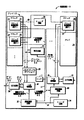
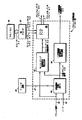
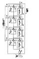
【解決手段】メモリは、各々メモリ・セル(48)とブロック制御回路(21;22)とを含む複数のメモリ・ブロック(17,18)と、第1の遅延を指示する第1の選択信号(62)を与える出力を有する第1の選択回路(24)と、各々第1の選択回路(24)の出力に結合されて第1の選択信号(62)を受け取る第1の複数のプログラマブル遅延回路(40)とを備える。第1の複数のプログラマブル遅延回路(40)の各々は、複数のメモリ・ブロック(17,18)のうちの1つのメモリ・ブロックのブロック制御回路に供給する出力信号(45)を与える出力を有する。
【選択図】図2
Description
Claims (4)
- メモリであって、
各々メモリ・セル(48)とブロック制御回路(21;22)とを含む複数のメモリ・ブロック(17,18)と、
第1の遅延を指示する第1の選択信号(62)を与える出力を有する第1の選択回路(24)と、
各々前記第1の選択回路(24)の出力に結合されて前記第1の選択信号(62)を受け取る第1の複数のプログラマブル遅延回路(40)とを備え、
前記第1の複数のプログラマブル遅延回路(40)の各々が、前記複数のメモリ・ブロック(17,18)のうちの1つのメモリ・ブロックの前記ブロック制御回路に供給する出力信号(45)を与える出力を有することを特徴とするメモリ。 - 請求項1に記載のメモリにおいて、
前記複数のメモリ・ブロックが第1〜第3メモリブロックを含むとともに、前記第1の複数のプログラマブル遅延回路が第1〜第3プログラマブル遅延回路を含み、
前記第1プログラマブル遅延回路(40)の出力が前記第1メモリブロック(17)に結合され、
前記第2プログラマブル遅延回路(40)の出力が前記第2メモリブロック(18)に結合され、
前記第3プログラマブル遅延回路(40)の出力が前記第3メモリブロックに結合されることを特徴とするメモリ。 - 請求項1に記載のメモリにおいて、
前記第1の複数のプログラマブル遅延回路(40)の各々は、前記複数のメモリ・ブロック(17,18)のうちの1つのメモリ・ブロックの前記ブロック制御回路(21;22)内か、またはその近くに配置されて、該ブロック制御回路に前記出力信号(45)を供給することを特徴とするメモリ。 - 請求項1に記載のメモリにおいて、
前記第1の遅延回路(24)の出力は、前記第1の遅延を固定遅延として指示する前記第1の選択信号(62)を継続的に与えることを特徴とするメモリ。
Applications Claiming Priority (2)
| Application Number | Priority Date | Filing Date | Title |
|---|---|---|---|
| US259454 | 1999-03-01 | ||
| US09/259,454 US6111796A (en) | 1999-03-01 | 1999-03-01 | Programmable delay control for sense amplifiers in a memory |
Related Parent Applications (1)
| Application Number | Title | Priority Date | Filing Date |
|---|---|---|---|
| JP27631799A Division JP4445074B2 (ja) | 1999-03-01 | 1999-09-29 | プログラマブル遅延制御機能を有する集積回路 |
Publications (2)
| Publication Number | Publication Date |
|---|---|
| JP2010003406A true JP2010003406A (ja) | 2010-01-07 |
| JP4903847B2 JP4903847B2 (ja) | 2012-03-28 |
Family
ID=22985023
Family Applications (2)
| Application Number | Title | Priority Date | Filing Date |
|---|---|---|---|
| JP27631799A Expired - Lifetime JP4445074B2 (ja) | 1999-03-01 | 1999-09-29 | プログラマブル遅延制御機能を有する集積回路 |
| JP2009230720A Expired - Lifetime JP4903847B2 (ja) | 1999-03-01 | 2009-10-02 | プログラマブル遅延制御機能を有する集積回路 |
Family Applications Before (1)
| Application Number | Title | Priority Date | Filing Date |
|---|---|---|---|
| JP27631799A Expired - Lifetime JP4445074B2 (ja) | 1999-03-01 | 1999-09-29 | プログラマブル遅延制御機能を有する集積回路 |
Country Status (8)
| Country | Link |
|---|---|
| US (2) | US6111796A (ja) |
| EP (3) | EP1770710B1 (ja) |
| JP (2) | JP4445074B2 (ja) |
| KR (1) | KR100665484B1 (ja) |
| CN (1) | CN1265509B (ja) |
| DE (1) | DE69942354D1 (ja) |
| SG (2) | SG100732A1 (ja) |
| TW (1) | TW440869B (ja) |
Cited By (1)
| Publication number | Priority date | Publication date | Assignee | Title |
|---|---|---|---|---|
| JP2012104207A (ja) * | 2010-11-12 | 2012-05-31 | Elpida Memory Inc | 半導体装置 |
Families Citing this family (45)
| Publication number | Priority date | Publication date | Assignee | Title |
|---|---|---|---|---|
| US6438043B2 (en) * | 1998-09-02 | 2002-08-20 | Micron Technology, Inc. | Adjustable I/O timing from externally applied voltage |
| US6111796A (en) * | 1999-03-01 | 2000-08-29 | Motorola, Inc. | Programmable delay control for sense amplifiers in a memory |
| US6877100B1 (en) * | 2000-08-25 | 2005-04-05 | Micron Technology, Inc. | Adjustable timing circuit of an integrated circuit by selecting and moving clock edges based on a signal propagation time stored in a programmable non-volatile fuse circuit |
| KR100389916B1 (ko) * | 2000-08-28 | 2003-07-04 | 삼성전자주식회사 | 메모리 모듈 및 메모리 컨트롤러 |
| DE10126312B4 (de) * | 2001-05-30 | 2015-10-22 | Infineon Technologies Ag | Halbleiterspeicher mit einem Signalpfad |
| US6721221B2 (en) * | 2001-06-08 | 2004-04-13 | Micron Technology, Inc. | Sense amplifier and architecture for open digit arrays |
| US6538932B2 (en) * | 2001-06-13 | 2003-03-25 | International Business Machines Corporation | Timing circuit and method for a compilable DRAM |
| JP3723477B2 (ja) * | 2001-09-06 | 2005-12-07 | 松下電器産業株式会社 | 半導体記憶装置 |
| KR100408420B1 (ko) * | 2002-01-09 | 2003-12-03 | 삼성전자주식회사 | 감지증폭기의 센싱속도를 향상시킬 수 있는 반도체메모리장치의 감지증폭기 구동회로 |
| US6947608B2 (en) * | 2002-01-25 | 2005-09-20 | Kabushiki Kaisha Toshiba | Equalizing circuit and method, and image processing circuit and method |
| US6762961B2 (en) | 2002-04-16 | 2004-07-13 | Sun Microsystems, Inc. | Variable delay compensation for data-dependent mismatch in characteristic of opposing devices of a sense amplifier |
| US7080275B2 (en) * | 2002-08-12 | 2006-07-18 | Micron Technology, Inc. | Method and apparatus using parasitic capacitance for synchronizing signals a device |
| US7177201B1 (en) | 2003-09-17 | 2007-02-13 | Sun Microsystems, Inc. | Negative bias temperature instability (NBTI) preconditioning of matched devices |
| US7020035B1 (en) | 2003-10-10 | 2006-03-28 | Sun Microsystems, Inc. | Measuring and correcting sense amplifier and memory mismatches using NBTI |
| TW200520388A (en) * | 2003-10-10 | 2005-06-16 | Atmel Corp | Selectable delay pulse generator |
| US7164612B1 (en) | 2003-10-10 | 2007-01-16 | Sun Microsystems, Inc. | Test circuit for measuring sense amplifier and memory mismatches |
| US6914467B2 (en) * | 2003-12-04 | 2005-07-05 | International Business Machines Corporation | Dual edge programmable delay unit |
| DE102004015868A1 (de) * | 2004-03-31 | 2005-10-27 | Micron Technology, Inc. | Rekonstruktion der Signalzeitgebung in integrierten Schaltungen |
| CN1947098A (zh) * | 2004-04-29 | 2007-04-11 | 皇家飞利浦电子股份有限公司 | 电子电路中的误差校正 |
| US6958943B1 (en) | 2004-05-12 | 2005-10-25 | International Business Machines Corporation | Programmable sense amplifier timing generator |
| US7222224B2 (en) * | 2004-05-21 | 2007-05-22 | Rambus Inc. | System and method for improving performance in computer memory systems supporting multiple memory access latencies |
| KR100555568B1 (ko) * | 2004-08-03 | 2006-03-03 | 삼성전자주식회사 | 온/오프 제어가 가능한 로컬 센스 증폭 회로를 구비하는반도체 메모리 장치 |
| US7157952B2 (en) * | 2004-08-20 | 2007-01-02 | L-3 Integrated Systems Company | Systems and methods for implementing delay line circuitry |
| EP1630815B1 (en) * | 2004-08-24 | 2011-10-05 | Infineon Technologies AG | Memory circuit with supply voltage flexibility and supply voltage adapted performance |
| KR100613073B1 (ko) | 2004-09-21 | 2006-08-16 | 주식회사 하이닉스반도체 | 센스 앰프 오버드라이브 회로 |
| KR100609621B1 (ko) | 2005-07-19 | 2006-08-08 | 삼성전자주식회사 | 메모리 블락별로 레이턴시 제어가 가능한 동기식 반도체메모리 장치 |
| US7215585B2 (en) * | 2005-09-01 | 2007-05-08 | Micron Technology, Inc. | Method and apparatus for synchronizing data from memory arrays |
| US7158432B1 (en) * | 2005-09-01 | 2007-01-02 | Freescale Semiconductor, Inc. | Memory with robust data sensing and method for sensing data |
| US8077533B2 (en) | 2006-01-23 | 2011-12-13 | Freescale Semiconductor, Inc. | Memory and method for sensing data in a memory using complementary sensing scheme |
| US7339842B1 (en) * | 2006-08-16 | 2008-03-04 | Arm Limited | Timing control for sense amplifiers in a memory circuit |
| KR100761381B1 (ko) * | 2006-09-06 | 2007-09-27 | 주식회사 하이닉스반도체 | 비트라인 센스앰프 미스매치판단이 가능한 메모리장치. |
| KR100824779B1 (ko) * | 2007-01-11 | 2008-04-24 | 삼성전자주식회사 | 반도체 메모리 장치의 데이터 출력 경로 및 데이터 출력방법 |
| KR100889311B1 (ko) * | 2007-02-23 | 2009-03-18 | 주식회사 하이닉스반도체 | 비트라인 감지증폭기를 포함하는 반도체메모리소자 |
| JP5102800B2 (ja) | 2009-04-15 | 2012-12-19 | インターナショナル・ビジネス・マシーンズ・コーポレーション | 半導体記憶装置 |
| KR20110025487A (ko) * | 2009-09-04 | 2011-03-10 | 삼성전자주식회사 | 반도체 메모리 장치 |
| JP5471761B2 (ja) * | 2010-04-15 | 2014-04-16 | 富士通株式会社 | 受信回路 |
| US9201096B2 (en) | 2010-09-08 | 2015-12-01 | Dcg Systems, Inc. | Laser-assisted device alteration using synchronized laser pulses |
| US8400852B2 (en) * | 2011-03-04 | 2013-03-19 | Taiwan Semiconductor Manufacturing Company, Ltd. | Circuit with remote amplifier |
| US8467254B2 (en) * | 2011-09-25 | 2013-06-18 | Nanya Technology Corporation | Memory apparatus |
| US8879303B2 (en) * | 2013-01-03 | 2014-11-04 | Lsi Corporation | Pre-charge tracking of global read lines in high speed SRAM |
| US11209985B2 (en) * | 2019-04-23 | 2021-12-28 | Macronix International Co., Ltd. | Input/output delay optimization method, electronic system and memory device using the same |
| CN112069768B (zh) * | 2020-09-08 | 2024-07-16 | 飞腾信息技术有限公司 | 一种针对双端口sram输入输出延时优化的方法 |
| KR102692866B1 (ko) * | 2021-04-26 | 2024-08-08 | 한국전자통신연구원 | 컴퓨팅 자원 분할 운용 방법 및 장치 |
| US12299296B2 (en) | 2022-03-10 | 2025-05-13 | Samsung Electronics Co., Ltd. | Semiconductor memory device and method of adjusting operation condition of the same |
| US12190994B2 (en) * | 2022-12-29 | 2025-01-07 | Xilinx, Inc. | Single port memory with multiple memory operations per clock cycle |
Citations (5)
| Publication number | Priority date | Publication date | Assignee | Title |
|---|---|---|---|---|
| JPH03225849A (ja) * | 1990-01-30 | 1991-10-04 | Nec Corp | 半導体装置 |
| JPH07264021A (ja) * | 1994-03-18 | 1995-10-13 | Fujitsu Ltd | 信号遅延回路及びプログラム可能な遅延回路 |
| JPH0973782A (ja) * | 1995-09-07 | 1997-03-18 | Fujitsu Ltd | 半導体記憶装置 |
| JPH1050063A (ja) * | 1996-07-30 | 1998-02-20 | Nec Corp | 半導体メモリ |
| JPH1083677A (ja) * | 1996-09-09 | 1998-03-31 | Hitachi Ltd | 半導体記憶装置及び半導体集積回路 |
Family Cites Families (21)
| Publication number | Priority date | Publication date | Assignee | Title |
|---|---|---|---|---|
| JPS63244494A (ja) * | 1987-03-31 | 1988-10-11 | Toshiba Corp | 半導体記憶装置 |
| US5028824A (en) * | 1989-05-05 | 1991-07-02 | Harris Corporation | Programmable delay circuit |
| US5289413A (en) * | 1990-06-08 | 1994-02-22 | Kabushiki Kaisha Toshiba | Dynamic semiconductor memory device with high-speed serial-accessing column decoder |
| US5204559A (en) * | 1991-01-23 | 1993-04-20 | Vitesse Semiconductor Corporation | Method and apparatus for controlling clock skew |
| US5321661A (en) * | 1991-11-20 | 1994-06-14 | Oki Electric Industry Co., Ltd. | Self-refreshing memory with on-chip timer test circuit |
| JP2982928B2 (ja) * | 1992-04-01 | 1999-11-29 | 三菱電機株式会社 | 半導体記憶装置 |
| EP0668591B1 (en) * | 1994-02-18 | 1999-10-20 | STMicroelectronics S.r.l. | Read timing method and circuit for nonvolatile memories |
| DE69424523T2 (de) * | 1994-02-18 | 2001-01-18 | Stmicroelectronics S.R.L., Agrate Brianza | Inneres Taktsteuerungsverfahren und Schaltung für programmierbare Speichern |
| KR0122108B1 (ko) * | 1994-06-10 | 1997-12-05 | 윤종용 | 반도체 메모리 장치의 비트라인 센싱회로 및 그 방법 |
| EP0720291B1 (en) * | 1994-12-20 | 2002-04-17 | Nec Corporation | Delay circuit device |
| US5933032A (en) * | 1995-12-29 | 1999-08-03 | Cypress Semiconductor Corp. | Apparatus and method for generating a pulse signal |
| JP3986578B2 (ja) * | 1996-01-17 | 2007-10-03 | 三菱電機株式会社 | 同期型半導体記憶装置 |
| TW340262B (en) | 1996-08-13 | 1998-09-11 | Fujitsu Ltd | Semiconductor device, system consisting of semiconductor devices and digital delay circuit |
| JPH1064275A (ja) * | 1996-08-27 | 1998-03-06 | Nkk Corp | 遅延回路、atdパルス発生回路、及びそれを用いた半導体記憶装置 |
| TW353176B (en) * | 1996-09-20 | 1999-02-21 | Hitachi Ltd | A semiconductor device capable of holding signals independent of the pulse width of an external clock and a computer system including the semiconductor |
| JPH10334665A (ja) * | 1997-05-30 | 1998-12-18 | Oki Micro Design Miyazaki:Kk | 半導体記憶装置 |
| US6247138B1 (en) * | 1997-06-12 | 2001-06-12 | Fujitsu Limited | Timing signal generating circuit, semiconductor integrated circuit device and semiconductor integrated circuit system to which the timing signal generating circuit is applied, and signal transmission system |
| US6009501A (en) * | 1997-06-18 | 1999-12-28 | Micron Technology, Inc. | Method and apparatus for local control signal generation in a memory device |
| US6031775A (en) * | 1999-03-01 | 2000-02-29 | Motorola Inc. | Dynamic sense amplifier in a memory capable of limiting the voltage swing on high-capacitance global data lines |
| US6111796A (en) * | 1999-03-01 | 2000-08-29 | Motorola, Inc. | Programmable delay control for sense amplifiers in a memory |
| US5978286A (en) * | 1999-03-01 | 1999-11-02 | Motorola, Inc. | Timing control of amplifiers in a memory |
-
1999
- 1999-03-01 US US09/259,454 patent/US6111796A/en not_active Expired - Lifetime
- 1999-09-15 SG SG200103540A patent/SG100732A1/en unknown
- 1999-09-15 SG SG9904489A patent/SG103248A1/en unknown
- 1999-09-20 DE DE69942354T patent/DE69942354D1/de not_active Expired - Lifetime
- 1999-09-20 EP EP06125239A patent/EP1770710B1/en not_active Expired - Lifetime
- 1999-09-20 EP EP06125238A patent/EP1770708B1/en not_active Expired - Lifetime
- 1999-09-20 EP EP99118540.6A patent/EP1033721B1/en not_active Expired - Lifetime
- 1999-09-27 KR KR1019990041318A patent/KR100665484B1/ko not_active Expired - Lifetime
- 1999-09-29 JP JP27631799A patent/JP4445074B2/ja not_active Expired - Lifetime
- 1999-09-30 TW TW088116845A patent/TW440869B/zh not_active IP Right Cessation
- 1999-10-21 CN CN99123118XA patent/CN1265509B/zh not_active Expired - Lifetime
-
2000
- 2000-04-06 US US09/543,532 patent/US6385101B1/en not_active Expired - Lifetime
-
2009
- 2009-10-02 JP JP2009230720A patent/JP4903847B2/ja not_active Expired - Lifetime
Patent Citations (5)
| Publication number | Priority date | Publication date | Assignee | Title |
|---|---|---|---|---|
| JPH03225849A (ja) * | 1990-01-30 | 1991-10-04 | Nec Corp | 半導体装置 |
| JPH07264021A (ja) * | 1994-03-18 | 1995-10-13 | Fujitsu Ltd | 信号遅延回路及びプログラム可能な遅延回路 |
| JPH0973782A (ja) * | 1995-09-07 | 1997-03-18 | Fujitsu Ltd | 半導体記憶装置 |
| JPH1050063A (ja) * | 1996-07-30 | 1998-02-20 | Nec Corp | 半導体メモリ |
| JPH1083677A (ja) * | 1996-09-09 | 1998-03-31 | Hitachi Ltd | 半導体記憶装置及び半導体集積回路 |
Cited By (1)
| Publication number | Priority date | Publication date | Assignee | Title |
|---|---|---|---|---|
| JP2012104207A (ja) * | 2010-11-12 | 2012-05-31 | Elpida Memory Inc | 半導体装置 |
Also Published As
| Publication number | Publication date |
|---|---|
| SG100732A1 (en) | 2003-12-26 |
| JP2000251472A (ja) | 2000-09-14 |
| EP1770710A2 (en) | 2007-04-04 |
| EP1770708A2 (en) | 2007-04-04 |
| KR100665484B1 (ko) | 2007-01-10 |
| EP1770708A3 (en) | 2007-07-04 |
| US6111796A (en) | 2000-08-29 |
| EP1033721B1 (en) | 2017-03-15 |
| EP1033721A2 (en) | 2000-09-06 |
| JP4903847B2 (ja) | 2012-03-28 |
| US6385101B1 (en) | 2002-05-07 |
| EP1770710B1 (en) | 2010-05-05 |
| DE69942354D1 (de) | 2010-06-17 |
| EP1770710A3 (en) | 2007-07-04 |
| KR20000062133A (ko) | 2000-10-25 |
| CN1265509A (zh) | 2000-09-06 |
| EP1033721A3 (en) | 2000-10-25 |
| SG103248A1 (en) | 2004-04-29 |
| EP1770708B1 (en) | 2012-11-14 |
| TW440869B (en) | 2001-06-16 |
| CN1265509B (zh) | 2010-10-27 |
| JP4445074B2 (ja) | 2010-04-07 |
Similar Documents
| Publication | Publication Date | Title |
|---|---|---|
| JP4903847B2 (ja) | プログラマブル遅延制御機能を有する集積回路 | |
| US5657292A (en) | Write pass through circuit | |
| US5864696A (en) | Circuit and method for setting the time duration of a write to a memory cell | |
| KR0141494B1 (ko) | 레벨시프트회로를 사용한 고속센스 방식의 반도체장치 | |
| JP5761873B2 (ja) | 使用される書き込みポートの数を変更可能なマルチポートメモリ | |
| US6031775A (en) | Dynamic sense amplifier in a memory capable of limiting the voltage swing on high-capacitance global data lines | |
| US5825691A (en) | Circuit and method for terminating a write to a memory cell | |
| CN110603591B (zh) | 用于半导体存储器的可配置命令及数据输入电路的设备及方法 | |
| US5619456A (en) | Synchronous output circuit | |
| JP3778381B2 (ja) | 半導体メモリ装置 | |
| JPH05325540A (ja) | 半導体記憶回路 | |
| JP4672116B2 (ja) | プログラマブル遅延を利用しアドレス・バッファを制御するメモリ | |
| US5808960A (en) | Circuit and method for tracking the start of a write to a memory cell | |
| KR20000052407A (ko) | 반도체 장치, 그 시험 방법 및 반도체 집적 회로 | |
| US5978286A (en) | Timing control of amplifiers in a memory | |
| US5511031A (en) | Semiconductor memory system having sense amplifier being activated late during clock cycle | |
| JPH097398A (ja) | テスト用書込回路を有する半導体メモリ装置 | |
| KR100650845B1 (ko) | 소비 전력을 감소시키는 버퍼 제어 회로와, 이를 포함하는메모리 모듈용 반도체 메모리 장치 및 그 제어 동작 방법 | |
| JPH0883491A (ja) | データ読出回路 | |
| JP2848117B2 (ja) | 半導体記憶回路 | |
| US6952372B2 (en) | Semiconductor memory device capable of testing data line redundancy replacement circuit | |
| JPH1031893A (ja) | 半導体記憶装置 | |
| JP2012253485A (ja) | 半導体装置 | |
| KR100337205B1 (ko) | 데이타 센스앰프 구동장치 | |
| US7339845B2 (en) | Memory device |
Legal Events
| Date | Code | Title | Description |
|---|---|---|---|
| A621 | Written request for application examination |
Free format text: JAPANESE INTERMEDIATE CODE: A621 Effective date: 20091023 |
|
| A131 | Notification of reasons for refusal |
Free format text: JAPANESE INTERMEDIATE CODE: A131 Effective date: 20110824 |
|
| A521 | Request for written amendment filed |
Free format text: JAPANESE INTERMEDIATE CODE: A523 Effective date: 20111118 |
|
| TRDD | Decision of grant or rejection written | ||
| A01 | Written decision to grant a patent or to grant a registration (utility model) |
Free format text: JAPANESE INTERMEDIATE CODE: A01 Effective date: 20111213 |
|
| A01 | Written decision to grant a patent or to grant a registration (utility model) |
Free format text: JAPANESE INTERMEDIATE CODE: A01 |
|
| A61 | First payment of annual fees (during grant procedure) |
Free format text: JAPANESE INTERMEDIATE CODE: A61 Effective date: 20120105 |
|
| R150 | Certificate of patent or registration of utility model |
Ref document number: 4903847 Country of ref document: JP Free format text: JAPANESE INTERMEDIATE CODE: R150 Free format text: JAPANESE INTERMEDIATE CODE: R150 |
|
| FPAY | Renewal fee payment (event date is renewal date of database) |
Free format text: PAYMENT UNTIL: 20150113 Year of fee payment: 3 |
|
| R250 | Receipt of annual fees |
Free format text: JAPANESE INTERMEDIATE CODE: R250 |
|
| R250 | Receipt of annual fees |
Free format text: JAPANESE INTERMEDIATE CODE: R250 |
|
| S111 | Request for change of ownership or part of ownership |
Free format text: JAPANESE INTERMEDIATE CODE: R313113 |
|
| S531 | Written request for registration of change of domicile |
Free format text: JAPANESE INTERMEDIATE CODE: R313531 |
|
| R350 | Written notification of registration of transfer |
Free format text: JAPANESE INTERMEDIATE CODE: R350 |
|
| R250 | Receipt of annual fees |
Free format text: JAPANESE INTERMEDIATE CODE: R250 |
|
| R250 | Receipt of annual fees |
Free format text: JAPANESE INTERMEDIATE CODE: R250 |
|
| R250 | Receipt of annual fees |
Free format text: JAPANESE INTERMEDIATE CODE: R250 |
|
| EXPY | Cancellation because of completion of term |