JP2009076658A - 半導体装置及びその製造方法 - Google Patents
半導体装置及びその製造方法 Download PDFInfo
- Publication number
- JP2009076658A JP2009076658A JP2007243944A JP2007243944A JP2009076658A JP 2009076658 A JP2009076658 A JP 2009076658A JP 2007243944 A JP2007243944 A JP 2007243944A JP 2007243944 A JP2007243944 A JP 2007243944A JP 2009076658 A JP2009076658 A JP 2009076658A
- Authority
- JP
- Japan
- Prior art keywords
- chip
- semiconductor device
- mounting portion
- support surface
- tab
- Prior art date
- Legal status (The legal status is an assumption and is not a legal conclusion. Google has not performed a legal analysis and makes no representation as to the accuracy of the status listed.)
- Pending
Links
- 239000004065 semiconductor Substances 0.000 title claims abstract description 168
- 238000004519 manufacturing process Methods 0.000 title claims description 23
- 238000007789 sealing Methods 0.000 claims abstract description 84
- 239000000463 material Substances 0.000 claims abstract description 37
- 230000002093 peripheral effect Effects 0.000 claims abstract description 24
- 238000000034 method Methods 0.000 claims description 41
- 239000011347 resin Substances 0.000 claims description 41
- 229920005989 resin Polymers 0.000 claims description 41
- 230000008569 process Effects 0.000 claims description 28
- 238000007747 plating Methods 0.000 claims description 23
- 238000005530 etching Methods 0.000 claims description 20
- 239000000725 suspension Substances 0.000 claims description 18
- 238000000465 moulding Methods 0.000 claims description 14
- 239000012790 adhesive layer Substances 0.000 claims description 12
- 230000015572 biosynthetic process Effects 0.000 claims description 7
- 238000004140 cleaning Methods 0.000 claims description 7
- 239000003960 organic solvent Substances 0.000 claims description 5
- 238000005520 cutting process Methods 0.000 claims description 3
- BQCADISMDOOEFD-UHFFFAOYSA-N Silver Chemical compound [Ag] BQCADISMDOOEFD-UHFFFAOYSA-N 0.000 abstract description 35
- 229910052709 silver Inorganic materials 0.000 abstract description 35
- 239000004332 silver Substances 0.000 abstract description 35
- 239000012535 impurity Substances 0.000 description 14
- 239000000243 solution Substances 0.000 description 11
- 230000000694 effects Effects 0.000 description 10
- 239000000126 substance Substances 0.000 description 8
- 230000017525 heat dissipation Effects 0.000 description 7
- 230000004048 modification Effects 0.000 description 6
- 238000012986 modification Methods 0.000 description 6
- 238000002347 injection Methods 0.000 description 5
- 239000007924 injection Substances 0.000 description 5
- 239000000853 adhesive Substances 0.000 description 3
- 230000001070 adhesive effect Effects 0.000 description 3
- 239000011248 coating agent Substances 0.000 description 3
- 238000000576 coating method Methods 0.000 description 3
- PCHJSUWPFVWCPO-UHFFFAOYSA-N gold Chemical compound [Au] PCHJSUWPFVWCPO-UHFFFAOYSA-N 0.000 description 3
- 239000012466 permeate Substances 0.000 description 3
- 239000000047 product Substances 0.000 description 3
- 238000000926 separation method Methods 0.000 description 3
- CSCPPACGZOOCGX-UHFFFAOYSA-N Acetone Chemical compound CC(C)=O CSCPPACGZOOCGX-UHFFFAOYSA-N 0.000 description 2
- 229910000881 Cu alloy Inorganic materials 0.000 description 2
- 238000004873 anchoring Methods 0.000 description 2
- 238000005452 bending Methods 0.000 description 2
- JWVAUCBYEDDGAD-UHFFFAOYSA-N bismuth tin Chemical compound [Sn].[Bi] JWVAUCBYEDDGAD-UHFFFAOYSA-N 0.000 description 2
- 238000002845 discoloration Methods 0.000 description 2
- 238000005516 engineering process Methods 0.000 description 2
- 229910052737 gold Inorganic materials 0.000 description 2
- 239000010931 gold Substances 0.000 description 2
- 238000007689 inspection Methods 0.000 description 2
- 229910000679 solder Inorganic materials 0.000 description 2
- 238000009736 wetting Methods 0.000 description 2
- 239000004593 Epoxy Substances 0.000 description 1
- 230000000712 assembly Effects 0.000 description 1
- 238000000429 assembly Methods 0.000 description 1
- 238000010586 diagram Methods 0.000 description 1
- 239000008393 encapsulating agent Substances 0.000 description 1
- 238000010438 heat treatment Methods 0.000 description 1
- 230000006872 improvement Effects 0.000 description 1
- 239000007788 liquid Substances 0.000 description 1
- 229910052751 metal Inorganic materials 0.000 description 1
- 239000002184 metal Substances 0.000 description 1
- 230000001151 other effect Effects 0.000 description 1
- 238000003825 pressing Methods 0.000 description 1
- 230000009467 reduction Effects 0.000 description 1
- 230000003252 repetitive effect Effects 0.000 description 1
- 230000000717 retained effect Effects 0.000 description 1
- 229910052710 silicon Inorganic materials 0.000 description 1
- 239000010703 silicon Substances 0.000 description 1
- 239000000758 substrate Substances 0.000 description 1
- 229920001187 thermosetting polymer Polymers 0.000 description 1
Images


Classifications
-
- H—ELECTRICITY
- H01—ELECTRIC ELEMENTS
- H01L—SEMICONDUCTOR DEVICES NOT COVERED BY CLASS H10
- H01L23/00—Details of semiconductor or other solid state devices
- H01L23/48—Arrangements for conducting electric current to or from the solid state body in operation, e.g. leads, terminal arrangements ; Selection of materials therefor
- H01L23/488—Arrangements for conducting electric current to or from the solid state body in operation, e.g. leads, terminal arrangements ; Selection of materials therefor consisting of soldered or bonded constructions
- H01L23/495—Lead-frames or other flat leads
- H01L23/49503—Lead-frames or other flat leads characterised by the die pad
-
- H—ELECTRICITY
- H01—ELECTRIC ELEMENTS
- H01L—SEMICONDUCTOR DEVICES NOT COVERED BY CLASS H10
- H01L21/00—Processes or apparatus adapted for the manufacture or treatment of semiconductor or solid state devices or of parts thereof
- H01L21/67—Apparatus specially adapted for handling semiconductor or electric solid state devices during manufacture or treatment thereof; Apparatus specially adapted for handling wafers during manufacture or treatment of semiconductor or electric solid state devices or components ; Apparatus not specifically provided for elsewhere
- H01L21/683—Apparatus specially adapted for handling semiconductor or electric solid state devices during manufacture or treatment thereof; Apparatus specially adapted for handling wafers during manufacture or treatment of semiconductor or electric solid state devices or components ; Apparatus not specifically provided for elsewhere for supporting or gripping
- H01L21/6835—Apparatus specially adapted for handling semiconductor or electric solid state devices during manufacture or treatment thereof; Apparatus specially adapted for handling wafers during manufacture or treatment of semiconductor or electric solid state devices or components ; Apparatus not specifically provided for elsewhere for supporting or gripping using temporarily an auxiliary support
-
- H—ELECTRICITY
- H01—ELECTRIC ELEMENTS
- H01L—SEMICONDUCTOR DEVICES NOT COVERED BY CLASS H10
- H01L23/00—Details of semiconductor or other solid state devices
- H01L23/48—Arrangements for conducting electric current to or from the solid state body in operation, e.g. leads, terminal arrangements ; Selection of materials therefor
- H01L23/488—Arrangements for conducting electric current to or from the solid state body in operation, e.g. leads, terminal arrangements ; Selection of materials therefor consisting of soldered or bonded constructions
- H01L23/495—Lead-frames or other flat leads
- H01L23/49541—Geometry of the lead-frame
- H01L23/49548—Cross section geometry
-
- H—ELECTRICITY
- H01—ELECTRIC ELEMENTS
- H01L—SEMICONDUCTOR DEVICES NOT COVERED BY CLASS H10
- H01L23/00—Details of semiconductor or other solid state devices
- H01L23/48—Arrangements for conducting electric current to or from the solid state body in operation, e.g. leads, terminal arrangements ; Selection of materials therefor
- H01L23/488—Arrangements for conducting electric current to or from the solid state body in operation, e.g. leads, terminal arrangements ; Selection of materials therefor consisting of soldered or bonded constructions
- H01L23/495—Lead-frames or other flat leads
- H01L23/49568—Lead-frames or other flat leads specifically adapted to facilitate heat dissipation
-
- H—ELECTRICITY
- H01—ELECTRIC ELEMENTS
- H01L—SEMICONDUCTOR DEVICES NOT COVERED BY CLASS H10
- H01L23/00—Details of semiconductor or other solid state devices
- H01L23/48—Arrangements for conducting electric current to or from the solid state body in operation, e.g. leads, terminal arrangements ; Selection of materials therefor
- H01L23/50—Arrangements for conducting electric current to or from the solid state body in operation, e.g. leads, terminal arrangements ; Selection of materials therefor for integrated circuit devices, e.g. power bus, number of leads
-
- H—ELECTRICITY
- H01—ELECTRIC ELEMENTS
- H01L—SEMICONDUCTOR DEVICES NOT COVERED BY CLASS H10
- H01L24/00—Arrangements for connecting or disconnecting semiconductor or solid-state bodies; Methods or apparatus related thereto
- H01L24/01—Means for bonding being attached to, or being formed on, the surface to be connected, e.g. chip-to-package, die-attach, "first-level" interconnects; Manufacturing methods related thereto
- H01L24/26—Layer connectors, e.g. plate connectors, solder or adhesive layers; Manufacturing methods related thereto
- H01L24/31—Structure, shape, material or disposition of the layer connectors after the connecting process
- H01L24/32—Structure, shape, material or disposition of the layer connectors after the connecting process of an individual layer connector
-
- H—ELECTRICITY
- H01—ELECTRIC ELEMENTS
- H01L—SEMICONDUCTOR DEVICES NOT COVERED BY CLASS H10
- H01L24/00—Arrangements for connecting or disconnecting semiconductor or solid-state bodies; Methods or apparatus related thereto
- H01L24/80—Methods for connecting semiconductor or other solid state bodies using means for bonding being attached to, or being formed on, the surface to be connected
- H01L24/83—Methods for connecting semiconductor or other solid state bodies using means for bonding being attached to, or being formed on, the surface to be connected using a layer connector
-
- H—ELECTRICITY
- H01—ELECTRIC ELEMENTS
- H01L—SEMICONDUCTOR DEVICES NOT COVERED BY CLASS H10
- H01L24/00—Arrangements for connecting or disconnecting semiconductor or solid-state bodies; Methods or apparatus related thereto
- H01L24/93—Batch processes
- H01L24/95—Batch processes at chip-level, i.e. with connecting carried out on a plurality of singulated devices, i.e. on diced chips
- H01L24/97—Batch processes at chip-level, i.e. with connecting carried out on a plurality of singulated devices, i.e. on diced chips the devices being connected to a common substrate, e.g. interposer, said common substrate being separable into individual assemblies after connecting
-
- H—ELECTRICITY
- H01—ELECTRIC ELEMENTS
- H01L—SEMICONDUCTOR DEVICES NOT COVERED BY CLASS H10
- H01L21/00—Processes or apparatus adapted for the manufacture or treatment of semiconductor or solid state devices or of parts thereof
- H01L21/02—Manufacture or treatment of semiconductor devices or of parts thereof
- H01L21/04—Manufacture or treatment of semiconductor devices or of parts thereof the devices having at least one potential-jump barrier or surface barrier, e.g. PN junction, depletion layer or carrier concentration layer
- H01L21/50—Assembly of semiconductor devices using processes or apparatus not provided for in a single one of the subgroups H01L21/06 - H01L21/326, e.g. sealing of a cap to a base of a container
- H01L21/56—Encapsulations, e.g. encapsulation layers, coatings
- H01L21/568—Temporary substrate used as encapsulation process aid
-
- H—ELECTRICITY
- H01—ELECTRIC ELEMENTS
- H01L—SEMICONDUCTOR DEVICES NOT COVERED BY CLASS H10
- H01L2224/00—Indexing scheme for arrangements for connecting or disconnecting semiconductor or solid-state bodies and methods related thereto as covered by H01L24/00
- H01L2224/01—Means for bonding being attached to, or being formed on, the surface to be connected, e.g. chip-to-package, die-attach, "first-level" interconnects; Manufacturing methods related thereto
- H01L2224/26—Layer connectors, e.g. plate connectors, solder or adhesive layers; Manufacturing methods related thereto
- H01L2224/27—Manufacturing methods
- H01L2224/27011—Involving a permanent auxiliary member, i.e. a member which is left at least partly in the finished device, e.g. coating, dummy feature
- H01L2224/27013—Involving a permanent auxiliary member, i.e. a member which is left at least partly in the finished device, e.g. coating, dummy feature for holding or confining the layer connector, e.g. solder flow barrier
-
- H—ELECTRICITY
- H01—ELECTRIC ELEMENTS
- H01L—SEMICONDUCTOR DEVICES NOT COVERED BY CLASS H10
- H01L2224/00—Indexing scheme for arrangements for connecting or disconnecting semiconductor or solid-state bodies and methods related thereto as covered by H01L24/00
- H01L2224/01—Means for bonding being attached to, or being formed on, the surface to be connected, e.g. chip-to-package, die-attach, "first-level" interconnects; Manufacturing methods related thereto
- H01L2224/26—Layer connectors, e.g. plate connectors, solder or adhesive layers; Manufacturing methods related thereto
- H01L2224/28—Structure, shape, material or disposition of the layer connectors prior to the connecting process
- H01L2224/29—Structure, shape, material or disposition of the layer connectors prior to the connecting process of an individual layer connector
- H01L2224/29001—Core members of the layer connector
- H01L2224/29005—Structure
- H01L2224/29007—Layer connector smaller than the underlying bonding area
-
- H—ELECTRICITY
- H01—ELECTRIC ELEMENTS
- H01L—SEMICONDUCTOR DEVICES NOT COVERED BY CLASS H10
- H01L2224/00—Indexing scheme for arrangements for connecting or disconnecting semiconductor or solid-state bodies and methods related thereto as covered by H01L24/00
- H01L2224/01—Means for bonding being attached to, or being formed on, the surface to be connected, e.g. chip-to-package, die-attach, "first-level" interconnects; Manufacturing methods related thereto
- H01L2224/26—Layer connectors, e.g. plate connectors, solder or adhesive layers; Manufacturing methods related thereto
- H01L2224/28—Structure, shape, material or disposition of the layer connectors prior to the connecting process
- H01L2224/29—Structure, shape, material or disposition of the layer connectors prior to the connecting process of an individual layer connector
- H01L2224/29001—Core members of the layer connector
- H01L2224/29099—Material
- H01L2224/2919—Material with a principal constituent of the material being a polymer, e.g. polyester, phenolic based polymer, epoxy
-
- H—ELECTRICITY
- H01—ELECTRIC ELEMENTS
- H01L—SEMICONDUCTOR DEVICES NOT COVERED BY CLASS H10
- H01L2224/00—Indexing scheme for arrangements for connecting or disconnecting semiconductor or solid-state bodies and methods related thereto as covered by H01L24/00
- H01L2224/01—Means for bonding being attached to, or being formed on, the surface to be connected, e.g. chip-to-package, die-attach, "first-level" interconnects; Manufacturing methods related thereto
- H01L2224/26—Layer connectors, e.g. plate connectors, solder or adhesive layers; Manufacturing methods related thereto
- H01L2224/28—Structure, shape, material or disposition of the layer connectors prior to the connecting process
- H01L2224/29—Structure, shape, material or disposition of the layer connectors prior to the connecting process of an individual layer connector
- H01L2224/29001—Core members of the layer connector
- H01L2224/29099—Material
- H01L2224/29198—Material with a principal constituent of the material being a combination of two or more materials in the form of a matrix with a filler, i.e. being a hybrid material, e.g. segmented structures, foams
- H01L2224/29298—Fillers
- H01L2224/29299—Base material
- H01L2224/293—Base material with a principal constituent of the material being a metal or a metalloid, e.g. boron [B], silicon [Si], germanium [Ge], arsenic [As], antimony [Sb], tellurium [Te] and polonium [Po], and alloys thereof
- H01L2224/29338—Base material with a principal constituent of the material being a metal or a metalloid, e.g. boron [B], silicon [Si], germanium [Ge], arsenic [As], antimony [Sb], tellurium [Te] and polonium [Po], and alloys thereof the principal constituent melting at a temperature of greater than or equal to 950°C and less than 1550°C
- H01L2224/29339—Silver [Ag] as principal constituent
-
- H—ELECTRICITY
- H01—ELECTRIC ELEMENTS
- H01L—SEMICONDUCTOR DEVICES NOT COVERED BY CLASS H10
- H01L2224/00—Indexing scheme for arrangements for connecting or disconnecting semiconductor or solid-state bodies and methods related thereto as covered by H01L24/00
- H01L2224/01—Means for bonding being attached to, or being formed on, the surface to be connected, e.g. chip-to-package, die-attach, "first-level" interconnects; Manufacturing methods related thereto
- H01L2224/26—Layer connectors, e.g. plate connectors, solder or adhesive layers; Manufacturing methods related thereto
- H01L2224/31—Structure, shape, material or disposition of the layer connectors after the connecting process
- H01L2224/32—Structure, shape, material or disposition of the layer connectors after the connecting process of an individual layer connector
- H01L2224/3201—Structure
- H01L2224/32012—Structure relative to the bonding area, e.g. bond pad
- H01L2224/32014—Structure relative to the bonding area, e.g. bond pad the layer connector being smaller than the bonding area, e.g. bond pad
-
- H—ELECTRICITY
- H01—ELECTRIC ELEMENTS
- H01L—SEMICONDUCTOR DEVICES NOT COVERED BY CLASS H10
- H01L2224/00—Indexing scheme for arrangements for connecting or disconnecting semiconductor or solid-state bodies and methods related thereto as covered by H01L24/00
- H01L2224/01—Means for bonding being attached to, or being formed on, the surface to be connected, e.g. chip-to-package, die-attach, "first-level" interconnects; Manufacturing methods related thereto
- H01L2224/26—Layer connectors, e.g. plate connectors, solder or adhesive layers; Manufacturing methods related thereto
- H01L2224/31—Structure, shape, material or disposition of the layer connectors after the connecting process
- H01L2224/32—Structure, shape, material or disposition of the layer connectors after the connecting process of an individual layer connector
- H01L2224/3205—Shape
- H01L2224/32057—Shape in side view
-
- H—ELECTRICITY
- H01—ELECTRIC ELEMENTS
- H01L—SEMICONDUCTOR DEVICES NOT COVERED BY CLASS H10
- H01L2224/00—Indexing scheme for arrangements for connecting or disconnecting semiconductor or solid-state bodies and methods related thereto as covered by H01L24/00
- H01L2224/01—Means for bonding being attached to, or being formed on, the surface to be connected, e.g. chip-to-package, die-attach, "first-level" interconnects; Manufacturing methods related thereto
- H01L2224/26—Layer connectors, e.g. plate connectors, solder or adhesive layers; Manufacturing methods related thereto
- H01L2224/31—Structure, shape, material or disposition of the layer connectors after the connecting process
- H01L2224/32—Structure, shape, material or disposition of the layer connectors after the connecting process of an individual layer connector
- H01L2224/321—Disposition
- H01L2224/32151—Disposition the layer connector connecting between a semiconductor or solid-state body and an item not being a semiconductor or solid-state body, e.g. chip-to-substrate, chip-to-passive
- H01L2224/32221—Disposition the layer connector connecting between a semiconductor or solid-state body and an item not being a semiconductor or solid-state body, e.g. chip-to-substrate, chip-to-passive the body and the item being stacked
- H01L2224/32245—Disposition the layer connector connecting between a semiconductor or solid-state body and an item not being a semiconductor or solid-state body, e.g. chip-to-substrate, chip-to-passive the body and the item being stacked the item being metallic
-
- H—ELECTRICITY
- H01—ELECTRIC ELEMENTS
- H01L—SEMICONDUCTOR DEVICES NOT COVERED BY CLASS H10
- H01L2224/00—Indexing scheme for arrangements for connecting or disconnecting semiconductor or solid-state bodies and methods related thereto as covered by H01L24/00
- H01L2224/01—Means for bonding being attached to, or being formed on, the surface to be connected, e.g. chip-to-package, die-attach, "first-level" interconnects; Manufacturing methods related thereto
- H01L2224/42—Wire connectors; Manufacturing methods related thereto
- H01L2224/44—Structure, shape, material or disposition of the wire connectors prior to the connecting process
- H01L2224/45—Structure, shape, material or disposition of the wire connectors prior to the connecting process of an individual wire connector
- H01L2224/45001—Core members of the connector
- H01L2224/45099—Material
- H01L2224/451—Material with a principal constituent of the material being a metal or a metalloid, e.g. boron (B), silicon (Si), germanium (Ge), arsenic (As), antimony (Sb), tellurium (Te) and polonium (Po), and alloys thereof
- H01L2224/45138—Material with a principal constituent of the material being a metal or a metalloid, e.g. boron (B), silicon (Si), germanium (Ge), arsenic (As), antimony (Sb), tellurium (Te) and polonium (Po), and alloys thereof the principal constituent melting at a temperature of greater than or equal to 950°C and less than 1550°C
- H01L2224/45144—Gold (Au) as principal constituent
-
- H—ELECTRICITY
- H01—ELECTRIC ELEMENTS
- H01L—SEMICONDUCTOR DEVICES NOT COVERED BY CLASS H10
- H01L2224/00—Indexing scheme for arrangements for connecting or disconnecting semiconductor or solid-state bodies and methods related thereto as covered by H01L24/00
- H01L2224/01—Means for bonding being attached to, or being formed on, the surface to be connected, e.g. chip-to-package, die-attach, "first-level" interconnects; Manufacturing methods related thereto
- H01L2224/42—Wire connectors; Manufacturing methods related thereto
- H01L2224/47—Structure, shape, material or disposition of the wire connectors after the connecting process
- H01L2224/48—Structure, shape, material or disposition of the wire connectors after the connecting process of an individual wire connector
- H01L2224/4805—Shape
- H01L2224/4809—Loop shape
- H01L2224/48091—Arched
-
- H—ELECTRICITY
- H01—ELECTRIC ELEMENTS
- H01L—SEMICONDUCTOR DEVICES NOT COVERED BY CLASS H10
- H01L2224/00—Indexing scheme for arrangements for connecting or disconnecting semiconductor or solid-state bodies and methods related thereto as covered by H01L24/00
- H01L2224/01—Means for bonding being attached to, or being formed on, the surface to be connected, e.g. chip-to-package, die-attach, "first-level" interconnects; Manufacturing methods related thereto
- H01L2224/42—Wire connectors; Manufacturing methods related thereto
- H01L2224/47—Structure, shape, material or disposition of the wire connectors after the connecting process
- H01L2224/48—Structure, shape, material or disposition of the wire connectors after the connecting process of an individual wire connector
- H01L2224/4805—Shape
- H01L2224/4809—Loop shape
- H01L2224/48095—Kinked
-
- H—ELECTRICITY
- H01—ELECTRIC ELEMENTS
- H01L—SEMICONDUCTOR DEVICES NOT COVERED BY CLASS H10
- H01L2224/00—Indexing scheme for arrangements for connecting or disconnecting semiconductor or solid-state bodies and methods related thereto as covered by H01L24/00
- H01L2224/01—Means for bonding being attached to, or being formed on, the surface to be connected, e.g. chip-to-package, die-attach, "first-level" interconnects; Manufacturing methods related thereto
- H01L2224/42—Wire connectors; Manufacturing methods related thereto
- H01L2224/47—Structure, shape, material or disposition of the wire connectors after the connecting process
- H01L2224/48—Structure, shape, material or disposition of the wire connectors after the connecting process of an individual wire connector
- H01L2224/481—Disposition
- H01L2224/48151—Connecting between a semiconductor or solid-state body and an item not being a semiconductor or solid-state body, e.g. chip-to-substrate, chip-to-passive
- H01L2224/48221—Connecting between a semiconductor or solid-state body and an item not being a semiconductor or solid-state body, e.g. chip-to-substrate, chip-to-passive the body and the item being stacked
- H01L2224/48245—Connecting between a semiconductor or solid-state body and an item not being a semiconductor or solid-state body, e.g. chip-to-substrate, chip-to-passive the body and the item being stacked the item being metallic
- H01L2224/48247—Connecting between a semiconductor or solid-state body and an item not being a semiconductor or solid-state body, e.g. chip-to-substrate, chip-to-passive the body and the item being stacked the item being metallic connecting the wire to a bond pad of the item
-
- H—ELECTRICITY
- H01—ELECTRIC ELEMENTS
- H01L—SEMICONDUCTOR DEVICES NOT COVERED BY CLASS H10
- H01L2224/00—Indexing scheme for arrangements for connecting or disconnecting semiconductor or solid-state bodies and methods related thereto as covered by H01L24/00
- H01L2224/01—Means for bonding being attached to, or being formed on, the surface to be connected, e.g. chip-to-package, die-attach, "first-level" interconnects; Manufacturing methods related thereto
- H01L2224/42—Wire connectors; Manufacturing methods related thereto
- H01L2224/47—Structure, shape, material or disposition of the wire connectors after the connecting process
- H01L2224/48—Structure, shape, material or disposition of the wire connectors after the connecting process of an individual wire connector
- H01L2224/484—Connecting portions
- H01L2224/48463—Connecting portions the connecting portion on the bonding area of the semiconductor or solid-state body being a ball bond
- H01L2224/48465—Connecting portions the connecting portion on the bonding area of the semiconductor or solid-state body being a ball bond the other connecting portion not on the bonding area being a wedge bond, i.e. ball-to-wedge, regular stitch
-
- H—ELECTRICITY
- H01—ELECTRIC ELEMENTS
- H01L—SEMICONDUCTOR DEVICES NOT COVERED BY CLASS H10
- H01L2224/00—Indexing scheme for arrangements for connecting or disconnecting semiconductor or solid-state bodies and methods related thereto as covered by H01L24/00
- H01L2224/01—Means for bonding being attached to, or being formed on, the surface to be connected, e.g. chip-to-package, die-attach, "first-level" interconnects; Manufacturing methods related thereto
- H01L2224/42—Wire connectors; Manufacturing methods related thereto
- H01L2224/47—Structure, shape, material or disposition of the wire connectors after the connecting process
- H01L2224/49—Structure, shape, material or disposition of the wire connectors after the connecting process of a plurality of wire connectors
- H01L2224/491—Disposition
- H01L2224/4912—Layout
- H01L2224/49175—Parallel arrangements
-
- H—ELECTRICITY
- H01—ELECTRIC ELEMENTS
- H01L—SEMICONDUCTOR DEVICES NOT COVERED BY CLASS H10
- H01L2224/00—Indexing scheme for arrangements for connecting or disconnecting semiconductor or solid-state bodies and methods related thereto as covered by H01L24/00
- H01L2224/73—Means for bonding being of different types provided for in two or more of groups H01L2224/10, H01L2224/18, H01L2224/26, H01L2224/34, H01L2224/42, H01L2224/50, H01L2224/63, H01L2224/71
- H01L2224/732—Location after the connecting process
- H01L2224/73251—Location after the connecting process on different surfaces
- H01L2224/73265—Layer and wire connectors
-
- H—ELECTRICITY
- H01—ELECTRIC ELEMENTS
- H01L—SEMICONDUCTOR DEVICES NOT COVERED BY CLASS H10
- H01L2224/00—Indexing scheme for arrangements for connecting or disconnecting semiconductor or solid-state bodies and methods related thereto as covered by H01L24/00
- H01L2224/80—Methods for connecting semiconductor or other solid state bodies using means for bonding being attached to, or being formed on, the surface to be connected
- H01L2224/83—Methods for connecting semiconductor or other solid state bodies using means for bonding being attached to, or being formed on, the surface to be connected using a layer connector
- H01L2224/83009—Pre-treatment of the layer connector or the bonding area
- H01L2224/83051—Forming additional members, e.g. dam structures
-
- H—ELECTRICITY
- H01—ELECTRIC ELEMENTS
- H01L—SEMICONDUCTOR DEVICES NOT COVERED BY CLASS H10
- H01L2224/00—Indexing scheme for arrangements for connecting or disconnecting semiconductor or solid-state bodies and methods related thereto as covered by H01L24/00
- H01L2224/80—Methods for connecting semiconductor or other solid state bodies using means for bonding being attached to, or being formed on, the surface to be connected
- H01L2224/83—Methods for connecting semiconductor or other solid state bodies using means for bonding being attached to, or being formed on, the surface to be connected using a layer connector
- H01L2224/8338—Bonding interfaces outside the semiconductor or solid-state body
- H01L2224/83385—Shape, e.g. interlocking features
-
- H—ELECTRICITY
- H01—ELECTRIC ELEMENTS
- H01L—SEMICONDUCTOR DEVICES NOT COVERED BY CLASS H10
- H01L2224/00—Indexing scheme for arrangements for connecting or disconnecting semiconductor or solid-state bodies and methods related thereto as covered by H01L24/00
- H01L2224/80—Methods for connecting semiconductor or other solid state bodies using means for bonding being attached to, or being formed on, the surface to be connected
- H01L2224/83—Methods for connecting semiconductor or other solid state bodies using means for bonding being attached to, or being formed on, the surface to be connected using a layer connector
- H01L2224/838—Bonding techniques
-
- H—ELECTRICITY
- H01—ELECTRIC ELEMENTS
- H01L—SEMICONDUCTOR DEVICES NOT COVERED BY CLASS H10
- H01L2224/00—Indexing scheme for arrangements for connecting or disconnecting semiconductor or solid-state bodies and methods related thereto as covered by H01L24/00
- H01L2224/93—Batch processes
- H01L2224/95—Batch processes at chip-level, i.e. with connecting carried out on a plurality of singulated devices, i.e. on diced chips
- H01L2224/97—Batch processes at chip-level, i.e. with connecting carried out on a plurality of singulated devices, i.e. on diced chips the devices being connected to a common substrate, e.g. interposer, said common substrate being separable into individual assemblies after connecting
-
- H—ELECTRICITY
- H01—ELECTRIC ELEMENTS
- H01L—SEMICONDUCTOR DEVICES NOT COVERED BY CLASS H10
- H01L23/00—Details of semiconductor or other solid state devices
- H01L23/48—Arrangements for conducting electric current to or from the solid state body in operation, e.g. leads, terminal arrangements ; Selection of materials therefor
- H01L23/488—Arrangements for conducting electric current to or from the solid state body in operation, e.g. leads, terminal arrangements ; Selection of materials therefor consisting of soldered or bonded constructions
- H01L23/495—Lead-frames or other flat leads
- H01L23/49579—Lead-frames or other flat leads characterised by the materials of the lead frames or layers thereon
- H01L23/49582—Metallic layers on lead frames
-
- H—ELECTRICITY
- H01—ELECTRIC ELEMENTS
- H01L—SEMICONDUCTOR DEVICES NOT COVERED BY CLASS H10
- H01L24/00—Arrangements for connecting or disconnecting semiconductor or solid-state bodies; Methods or apparatus related thereto
- H01L24/01—Means for bonding being attached to, or being formed on, the surface to be connected, e.g. chip-to-package, die-attach, "first-level" interconnects; Manufacturing methods related thereto
- H01L24/26—Layer connectors, e.g. plate connectors, solder or adhesive layers; Manufacturing methods related thereto
- H01L24/28—Structure, shape, material or disposition of the layer connectors prior to the connecting process
-
- H—ELECTRICITY
- H01—ELECTRIC ELEMENTS
- H01L—SEMICONDUCTOR DEVICES NOT COVERED BY CLASS H10
- H01L24/00—Arrangements for connecting or disconnecting semiconductor or solid-state bodies; Methods or apparatus related thereto
- H01L24/01—Means for bonding being attached to, or being formed on, the surface to be connected, e.g. chip-to-package, die-attach, "first-level" interconnects; Manufacturing methods related thereto
- H01L24/42—Wire connectors; Manufacturing methods related thereto
- H01L24/44—Structure, shape, material or disposition of the wire connectors prior to the connecting process
- H01L24/45—Structure, shape, material or disposition of the wire connectors prior to the connecting process of an individual wire connector
-
- H—ELECTRICITY
- H01—ELECTRIC ELEMENTS
- H01L—SEMICONDUCTOR DEVICES NOT COVERED BY CLASS H10
- H01L24/00—Arrangements for connecting or disconnecting semiconductor or solid-state bodies; Methods or apparatus related thereto
- H01L24/01—Means for bonding being attached to, or being formed on, the surface to be connected, e.g. chip-to-package, die-attach, "first-level" interconnects; Manufacturing methods related thereto
- H01L24/42—Wire connectors; Manufacturing methods related thereto
- H01L24/47—Structure, shape, material or disposition of the wire connectors after the connecting process
- H01L24/48—Structure, shape, material or disposition of the wire connectors after the connecting process of an individual wire connector
-
- H—ELECTRICITY
- H01—ELECTRIC ELEMENTS
- H01L—SEMICONDUCTOR DEVICES NOT COVERED BY CLASS H10
- H01L24/00—Arrangements for connecting or disconnecting semiconductor or solid-state bodies; Methods or apparatus related thereto
- H01L24/01—Means for bonding being attached to, or being formed on, the surface to be connected, e.g. chip-to-package, die-attach, "first-level" interconnects; Manufacturing methods related thereto
- H01L24/42—Wire connectors; Manufacturing methods related thereto
- H01L24/47—Structure, shape, material or disposition of the wire connectors after the connecting process
- H01L24/49—Structure, shape, material or disposition of the wire connectors after the connecting process of a plurality of wire connectors
-
- H—ELECTRICITY
- H01—ELECTRIC ELEMENTS
- H01L—SEMICONDUCTOR DEVICES NOT COVERED BY CLASS H10
- H01L24/00—Arrangements for connecting or disconnecting semiconductor or solid-state bodies; Methods or apparatus related thereto
- H01L24/73—Means for bonding being of different types provided for in two or more of groups H01L24/10, H01L24/18, H01L24/26, H01L24/34, H01L24/42, H01L24/50, H01L24/63, H01L24/71
-
- H—ELECTRICITY
- H01—ELECTRIC ELEMENTS
- H01L—SEMICONDUCTOR DEVICES NOT COVERED BY CLASS H10
- H01L2924/00—Indexing scheme for arrangements or methods for connecting or disconnecting semiconductor or solid-state bodies as covered by H01L24/00
- H01L2924/01—Chemical elements
- H01L2924/01005—Boron [B]
-
- H—ELECTRICITY
- H01—ELECTRIC ELEMENTS
- H01L—SEMICONDUCTOR DEVICES NOT COVERED BY CLASS H10
- H01L2924/00—Indexing scheme for arrangements or methods for connecting or disconnecting semiconductor or solid-state bodies as covered by H01L24/00
- H01L2924/01—Chemical elements
- H01L2924/01006—Carbon [C]
-
- H—ELECTRICITY
- H01—ELECTRIC ELEMENTS
- H01L—SEMICONDUCTOR DEVICES NOT COVERED BY CLASS H10
- H01L2924/00—Indexing scheme for arrangements or methods for connecting or disconnecting semiconductor or solid-state bodies as covered by H01L24/00
- H01L2924/01—Chemical elements
- H01L2924/01014—Silicon [Si]
-
- H—ELECTRICITY
- H01—ELECTRIC ELEMENTS
- H01L—SEMICONDUCTOR DEVICES NOT COVERED BY CLASS H10
- H01L2924/00—Indexing scheme for arrangements or methods for connecting or disconnecting semiconductor or solid-state bodies as covered by H01L24/00
- H01L2924/01—Chemical elements
- H01L2924/01029—Copper [Cu]
-
- H—ELECTRICITY
- H01—ELECTRIC ELEMENTS
- H01L—SEMICONDUCTOR DEVICES NOT COVERED BY CLASS H10
- H01L2924/00—Indexing scheme for arrangements or methods for connecting or disconnecting semiconductor or solid-state bodies as covered by H01L24/00
- H01L2924/01—Chemical elements
- H01L2924/01033—Arsenic [As]
-
- H—ELECTRICITY
- H01—ELECTRIC ELEMENTS
- H01L—SEMICONDUCTOR DEVICES NOT COVERED BY CLASS H10
- H01L2924/00—Indexing scheme for arrangements or methods for connecting or disconnecting semiconductor or solid-state bodies as covered by H01L24/00
- H01L2924/01—Chemical elements
- H01L2924/01047—Silver [Ag]
-
- H—ELECTRICITY
- H01—ELECTRIC ELEMENTS
- H01L—SEMICONDUCTOR DEVICES NOT COVERED BY CLASS H10
- H01L2924/00—Indexing scheme for arrangements or methods for connecting or disconnecting semiconductor or solid-state bodies as covered by H01L24/00
- H01L2924/01—Chemical elements
- H01L2924/0105—Tin [Sn]
-
- H—ELECTRICITY
- H01—ELECTRIC ELEMENTS
- H01L—SEMICONDUCTOR DEVICES NOT COVERED BY CLASS H10
- H01L2924/00—Indexing scheme for arrangements or methods for connecting or disconnecting semiconductor or solid-state bodies as covered by H01L24/00
- H01L2924/01—Chemical elements
- H01L2924/01078—Platinum [Pt]
-
- H—ELECTRICITY
- H01—ELECTRIC ELEMENTS
- H01L—SEMICONDUCTOR DEVICES NOT COVERED BY CLASS H10
- H01L2924/00—Indexing scheme for arrangements or methods for connecting or disconnecting semiconductor or solid-state bodies as covered by H01L24/00
- H01L2924/01—Chemical elements
- H01L2924/01079—Gold [Au]
-
- H—ELECTRICITY
- H01—ELECTRIC ELEMENTS
- H01L—SEMICONDUCTOR DEVICES NOT COVERED BY CLASS H10
- H01L2924/00—Indexing scheme for arrangements or methods for connecting or disconnecting semiconductor or solid-state bodies as covered by H01L24/00
- H01L2924/01—Chemical elements
- H01L2924/01082—Lead [Pb]
-
- H—ELECTRICITY
- H01—ELECTRIC ELEMENTS
- H01L—SEMICONDUCTOR DEVICES NOT COVERED BY CLASS H10
- H01L2924/00—Indexing scheme for arrangements or methods for connecting or disconnecting semiconductor or solid-state bodies as covered by H01L24/00
- H01L2924/013—Alloys
- H01L2924/014—Solder alloys
-
- H—ELECTRICITY
- H01—ELECTRIC ELEMENTS
- H01L—SEMICONDUCTOR DEVICES NOT COVERED BY CLASS H10
- H01L2924/00—Indexing scheme for arrangements or methods for connecting or disconnecting semiconductor or solid-state bodies as covered by H01L24/00
- H01L2924/06—Polymers
- H01L2924/0665—Epoxy resin
-
- H—ELECTRICITY
- H01—ELECTRIC ELEMENTS
- H01L—SEMICONDUCTOR DEVICES NOT COVERED BY CLASS H10
- H01L2924/00—Indexing scheme for arrangements or methods for connecting or disconnecting semiconductor or solid-state bodies as covered by H01L24/00
- H01L2924/06—Polymers
- H01L2924/078—Adhesive characteristics other than chemical
- H01L2924/0781—Adhesive characteristics other than chemical being an ohmic electrical conductor
-
- H—ELECTRICITY
- H01—ELECTRIC ELEMENTS
- H01L—SEMICONDUCTOR DEVICES NOT COVERED BY CLASS H10
- H01L2924/00—Indexing scheme for arrangements or methods for connecting or disconnecting semiconductor or solid-state bodies as covered by H01L24/00
- H01L2924/15—Details of package parts other than the semiconductor or other solid state devices to be connected
- H01L2924/181—Encapsulation
- H01L2924/183—Connection portion, e.g. seal
- H01L2924/18301—Connection portion, e.g. seal being an anchoring portion, i.e. mechanical interlocking between the encapsulation resin and another package part
Abstract
【解決手段】タブ1bと、タブ1bの周囲に配置された複数のリード1aと、タブ1bのチップ支持面1c上に配置された銀ペースト6と、タブ1b上に銀ペースト6を介して搭載された半導体チップ2とを有している。さらに、半導体チップ2のパッド2aとリード1aとを電気的に接続する複数のワイヤ4と、半導体チップ2と複数のワイヤ4を樹脂封止する封止体3とを有しており、タブ1bのチップ支持面1cの周縁部にチップ支持面1cより高さの低い段差部1eが形成されていることにより、タブ1bからはみ出した銀ペースト6をこの段差部1eに留めることができ、その結果、銀ペースト6の封止体3の裏面3aへの流出を防ぐことができる。
【選択図】図5
Description
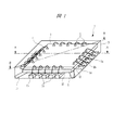
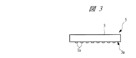
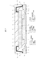
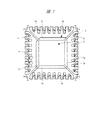
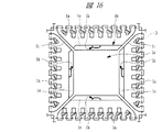
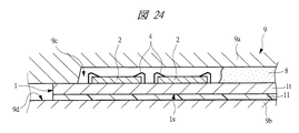
図1は本発明の実施の形態1の半導体装置の構造の一例を封止体を透過して示す斜視図、図2は図1に示す半導体装置の構造を示す平面図、図3は図1に示す半導体装置の構造を示す側面図、図4は図1に示す半導体装置の構造を示す裏面図、図5は図1に示すA−A線に沿って切断した構造の一例を示す断面図、図6は図1に示すB−B線に沿って切断した構造の一例を示す断面図、図7は図1に示す半導体装置におけるタブ、吊りリード、及びリードの構造を封止体を透過して示す部分平面図、図8は図7に示すC−C線に沿って切断した断面図、図9は図8の変形例図である。
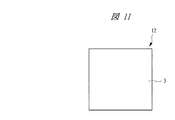
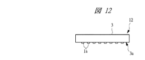
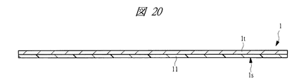
図10は本発明の実施の形態2の半導体装置の構造の一例を封止体を透過して示す斜視図、図11は図10に示す半導体装置の構造を示す平面図、図12は図10に示す半導体装置の構造を示す側面図、図13は図10に示す半導体装置の構造を示す裏面図、図14は図10に示すA−A線に沿って切断した構造の一例を示す断面図、図15は図10に示すB−B線に沿って切断した構造の一例を示す断面図である。また、図16は図10に示す半導体装置におけるタブと突起部の構造を封止体を透過して示す部分平面図、図17は本発明の実施の形態2の変形例の半導体装置におけるタブと突起部の構造を封止体を透過して示す部分平面図、図18は本発明の実施の形態2の半導体装置の組み立て順の一例を示す製造フロー図である。さらに、図19は本発明の実施の形態2の半導体装置の組み立てに用いられるテープ付きリードフレームの構造の一例を示す平面図、図20は図19に示すテープ付きリードフレームの構造の一例を示す断面図、図21は図19に示すテープ付きリードフレームに貼り付けられたテープの構造の一例を示す断面図である。
1a リード
1b タブ(チップ搭載部)
1c チップ支持面
1d 裏面
1e 段差部
1f 第1肉薄部
1g 実装面
1h ワイヤ接続面
1i 吊りリード
1j 第2肉薄部
1k 突起部
1m 抉れ部
1n デバイス領域(半導体装置形成領域)
1p 枠部
1q スリット
1r ガイド孔
1s 裏面
1t フレーム本体
2 半導体チップ
2a パッド(電極)
2b 主面
2c 裏面
3 封止体
3a 裏面
3b 側面
4 ワイヤ
5 QFN(半導体装置)
6 銀ペースト(ペースト材)
7 外装めっき
8 封止用樹脂
9 樹脂成形金型
9a 上型
9b 下型
9c キャビティ
9d 金型面
10 一括封止体
11 テープ
11a 基材
11b 接着層
12 QFN(半導体装置)
Claims (17)
- チップ支持面を備えたチップ搭載部と、
前記チップ搭載部の周囲に配置された複数のリードと、
前記チップ搭載部の前記チップ支持面上に配置されたペースト材と、
前記チップ搭載部の前記チップ支持面上に前記ペースト材を介して搭載された半導体チップと、
前記半導体チップの複数の電極と前記複数のリードとをそれぞれ電気的に接続する複数のワイヤと、
前記半導体チップと前記複数のワイヤと前記複数のリードそれぞれの一部と前記チップ搭載部の一部を樹脂封止する封止体とを有し、
前記チップ搭載部の前記チップ支持面の外形サイズは、前記半導体チップの裏面より小さく、
前記チップ搭載部の前記チップ支持面と反対側の裏面は前記封止体から露出し、
前記チップ搭載部の前記チップ支持面の周縁部に前記チップ支持面より高さの低い段差部が形成されていることを特徴とする半導体装置。 - 請求項1記載の半導体装置において、前記複数のリードそれぞれのチップ側の端部は、前記半導体チップの裏面と対向していることを特徴とする半導体装置。
- 請求項2記載の半導体装置において、前記複数のリードそれぞれのチップ側の端部に第1肉薄部が形成され、前記第1肉薄部が前記半導体チップの裏面と対向していることを特徴とする半導体装置。
- 請求項1記載の半導体装置において、前記チップ搭載部の前記チップ支持面と、前記複数のリードそれぞれのワイヤ接続面は同じ高さであることを特徴とする半導体装置。
- 請求項1記載の半導体装置において、前記チップ搭載部と連結する吊りリードを有し、前記吊りリードはエッチングによって形成された第2肉薄部を備え、前記第2肉薄部は前記封止体内に埋め込まれていることを特徴とする半導体装置。
- 請求項1記載の半導体装置において、前記チップ搭載部の前記チップ支持面の全面に前記ペースト材が配置されていることを特徴とする半導体装置。
- 請求項1記載の半導体装置において、前記チップ搭載部の前記段差部に前記半導体チップに向かって突出した突起部が形成されていることを特徴とする半導体装置。
- 請求項7記載の半導体装置において、前記チップ搭載部の前記チップ支持面が四角形を成し、前記四角形の前記チップ支持面の各辺にこの各辺に設けられた前記突起部から遠ざかる方向に抉れた抉れ部が形成されていることを特徴とする半導体装置。
- 請求項7記載の半導体装置において、前記突起部は、四角形の前記チップ搭載部の1つの辺に対応した前記段差部の中央部に形成されていることを特徴とする半導体装置。
- 請求項7記載の半導体装置において、前記突起部は、四角形の前記チップ搭載部の1つの辺に対応した前記段差部に1つずつ形成されていることを特徴とする半導体装置。
- (a)チップ支持面の周縁部に前記チップ支持面より高さの低い段差部が形成されたチップ搭載部と、前記チップ搭載部の周囲に配置された複数のリードとを有するリードフレームを準備する工程と、
(b)前記チップ搭載部の前記チップ支持面上にペースト材を塗布する工程と、
(c)半導体チップの裏面より外形サイズが小さな前記チップ搭載部の前記チップ支持面上に前記ペースト材を介して半導体チップを接合する工程と、
(d)前記半導体チップの複数の電極と前記複数のリードとをそれぞれ電気的に接続する工程と、
(e)複数の半導体装置形成領域を樹脂成形金型の1つのキャビティで覆った状態で封止用樹脂を前記キャビティ内に注入し、前記半導体チップと前記チップ搭載部の前記段差部との間に封止用樹脂を周り込ませ、かつ前記チップ搭載部の前記チップ支持面と反対側の裏面及び前記複数のリードそれぞれの一部が露出するように前記半導体チップと複数のワイヤを樹脂封止して一括封止体を形成する工程と、
(f)前記一括封止体及び前記リードフレームを切断して各半導体装置に個片化する工程とを有することを特徴とする半導体装置の製造方法。 - 請求項11記載の半導体装置の製造方法において、前記(e)工程で、接着層を有するテープを前記リードフレームの裏面に貼り付けた状態で前記樹脂成形金型をクランプし、この状態で前記封止用樹脂を前記キャビティ内に注入して前記一括封止体を形成することを特徴とする半導体装置の製造方法。
- 請求項11記載の半導体装置の製造方法において、前記(e)工程の後、前記リードフレームの裏面から前記テープを剥離する剥離工程を有することを特徴とする半導体装置の製造方法。
- 請求項11記載の半導体装置の製造方法において、前記(e)工程の後、前記リードフレームの裏面から前記テープを剥離する剥離工程を有し、さらに前記剥離工程の後に、前記リードフレームの裏面を洗浄する洗浄工程を有することを特徴とする半導体装置の製造方法。
- 請求項14記載の半導体装置の製造方法において、前記洗浄工程で、有機系溶剤によって前記リードフレームの裏面を洗浄することを特徴とする半導体装置の製造方法。
- 請求項14記載の半導体装置の製造方法において、前記洗浄工程の後に、前記一括封止体から露出する前記チップ搭載部の裏面及び前記複数のリードそれぞれの一部に外装めっきを形成するめっき処理工程を有することを特徴とする半導体装置の製造方法。
- 請求項11記載の半導体装置の製造方法において、前記チップ搭載部の前記段差部に前記半導体チップに向かって突出した突起部がエッチングにより形成されていることを特徴とする半導体装置の製造方法。
Priority Applications (6)
| Application Number | Priority Date | Filing Date | Title |
|---|---|---|---|
| JP2007243944A JP2009076658A (ja) | 2007-09-20 | 2007-09-20 | 半導体装置及びその製造方法 |
| TW097123763A TW200924145A (en) | 2007-09-20 | 2008-06-25 | Semiconductor device and manufacturing method of the same |
| US12/147,676 US8558362B2 (en) | 2007-09-20 | 2008-06-27 | Semiconductor device and manufacturing method of the same |
| CN201310224828.0A CN103295995B (zh) | 2007-09-20 | 2008-08-12 | 半导体器件及其制造方法 |
| CNA200810210915XA CN101393900A (zh) | 2007-09-20 | 2008-08-12 | 半导体器件及其制造方法 |
| KR1020080092006A KR20090031279A (ko) | 2007-09-20 | 2008-09-19 | 반도체 장치 및 그 제조 방법 |
Applications Claiming Priority (1)
| Application Number | Priority Date | Filing Date | Title |
|---|---|---|---|
| JP2007243944A JP2009076658A (ja) | 2007-09-20 | 2007-09-20 | 半導体装置及びその製造方法 |
Publications (2)
| Publication Number | Publication Date |
|---|---|
| JP2009076658A true JP2009076658A (ja) | 2009-04-09 |
| JP2009076658A5 JP2009076658A5 (ja) | 2010-10-28 |
Family
ID=40470750
Family Applications (1)
| Application Number | Title | Priority Date | Filing Date |
|---|---|---|---|
| JP2007243944A Pending JP2009076658A (ja) | 2007-09-20 | 2007-09-20 | 半導体装置及びその製造方法 |
Country Status (5)
| Country | Link |
|---|---|
| US (1) | US8558362B2 (ja) |
| JP (1) | JP2009076658A (ja) |
| KR (1) | KR20090031279A (ja) |
| CN (2) | CN103295995B (ja) |
| TW (1) | TW200924145A (ja) |
Cited By (3)
| Publication number | Priority date | Publication date | Assignee | Title |
|---|---|---|---|---|
| JP2013118215A (ja) * | 2011-12-01 | 2013-06-13 | Renesas Electronics Corp | 半導体装置 |
| KR20160089274A (ko) * | 2014-12-23 | 2016-07-27 | 인텔 코포레이션 | 패키지 온 패키지 제품을 위한 와이어 리드를 갖는 집적 패키지 설계 |
| JPWO2021152795A1 (ja) * | 2020-01-30 | 2021-08-05 |
Families Citing this family (20)
| Publication number | Priority date | Publication date | Assignee | Title |
|---|---|---|---|---|
| CN201838585U (zh) * | 2010-06-17 | 2011-05-18 | 国碁电子(中山)有限公司 | 堆叠式芯片封装结构及其基板 |
| JP2012028744A (ja) * | 2010-06-22 | 2012-02-09 | Panasonic Corp | 半導体装置用パッケージおよびその製造方法ならびに半導体装置 |
| JP5437943B2 (ja) * | 2010-07-26 | 2014-03-12 | 日立オートモティブシステムズ株式会社 | パワー半導体ユニット、パワーモジュールおよびそれらの製造方法 |
| TWI431218B (zh) * | 2011-03-11 | 2014-03-21 | Lingsen Precision Ind Ltd | The manufacturing method and structure of LED light bar |
| TWI608062B (zh) * | 2011-05-31 | 2017-12-11 | 住友電木股份有限公司 | 樹脂組成物、使用它之半導體裝置及半導體裝置之製造方法 |
| JP6076675B2 (ja) * | 2011-10-31 | 2017-02-08 | ローム株式会社 | 半導体装置 |
| US9711424B2 (en) * | 2012-09-17 | 2017-07-18 | Littelfuse, Inc. | Low thermal stress package for large area semiconductor dies |
| JP5970316B2 (ja) * | 2012-09-26 | 2016-08-17 | ルネサスエレクトロニクス株式会社 | 半導体装置の製造方法 |
| JP6092645B2 (ja) * | 2013-02-07 | 2017-03-08 | エスアイアイ・セミコンダクタ株式会社 | 半導体装置 |
| JP2014203861A (ja) | 2013-04-02 | 2014-10-27 | 三菱電機株式会社 | 半導体装置および半導体モジュール |
| US9054092B2 (en) * | 2013-10-28 | 2015-06-09 | Texas Instruments Incorporated | Method and apparatus for stopping resin bleed and mold flash on integrated circuit lead finishes |
| CN105097431A (zh) * | 2014-05-09 | 2015-11-25 | 中芯国际集成电路制造(上海)有限公司 | 一种晶圆正面的保护方法 |
| US9589871B2 (en) * | 2015-04-13 | 2017-03-07 | Advanced Semiconductor Engineering, Inc. | Semiconductor package structure and method for manufacturing the same |
| WO2016207999A1 (ja) * | 2015-06-24 | 2016-12-29 | ルネサスエレクトロニクス株式会社 | 半導体装置の製造方法 |
| US9490222B1 (en) * | 2015-10-12 | 2016-11-08 | Invensas Corporation | Wire bond wires for interference shielding |
| US9824959B2 (en) * | 2016-03-23 | 2017-11-21 | Texas Instruments Incorporated | Structure and method for stabilizing leads in wire-bonded semiconductor devices |
| JP7182374B2 (ja) * | 2017-05-15 | 2022-12-02 | 新光電気工業株式会社 | リードフレーム及びその製造方法 |
| JP2020088066A (ja) | 2018-11-20 | 2020-06-04 | キヤノン株式会社 | 電子部品および機器 |
| JP7338204B2 (ja) * | 2019-04-01 | 2023-09-05 | 富士電機株式会社 | 半導体装置 |
| CN111540691A (zh) * | 2020-05-22 | 2020-08-14 | 东莞链芯半导体科技有限公司 | 半导体封装结构及其封装方法 |
Citations (10)
| Publication number | Priority date | Publication date | Assignee | Title |
|---|---|---|---|---|
| JP2002246529A (ja) * | 2001-02-14 | 2002-08-30 | Matsushita Electric Ind Co Ltd | 樹脂封止型半導体装置及びその製造方法 |
| JP2002261187A (ja) * | 2000-12-28 | 2002-09-13 | Hitachi Ltd | 半導体装置 |
| JP2003037219A (ja) * | 2001-07-23 | 2003-02-07 | Matsushita Electric Ind Co Ltd | 樹脂封止型半導体装置およびその製造方法 |
| JP2003124421A (ja) * | 2001-10-15 | 2003-04-25 | Shinko Electric Ind Co Ltd | リードフレーム及びその製造方法並びに該リードフレームを用いた半導体装置の製造方法 |
| JP2004146562A (ja) * | 2002-10-24 | 2004-05-20 | Matsushita Electric Ind Co Ltd | リードフレームとそれを用いた樹脂封止型半導体装置およびその製造方法 |
| JP2004235217A (ja) * | 2003-01-28 | 2004-08-19 | Renesas Technology Corp | 半導体装置及び電子装置の製造方法 |
| JP2005166943A (ja) * | 2003-12-02 | 2005-06-23 | Sony Corp | リードフレーム、それを用いた半導体装置の製造におけるワイヤーボンディング方法及び樹脂封止型半導体装置 |
| JP2005294443A (ja) * | 2004-03-31 | 2005-10-20 | Sony Corp | 半導体装置及びその製造方法 |
| JP2006318996A (ja) * | 2005-05-10 | 2006-11-24 | Matsushita Electric Ind Co Ltd | リードフレームおよび樹脂封止型半導体装置 |
| US7227245B1 (en) * | 2004-02-26 | 2007-06-05 | National Semiconductor Corporation | Die attach pad for use in semiconductor manufacturing and method of making same |
Family Cites Families (8)
| Publication number | Priority date | Publication date | Assignee | Title |
|---|---|---|---|---|
| KR100552353B1 (ko) | 1992-03-27 | 2006-06-20 | 가부시키가이샤 히타치초엘에스아이시스템즈 | 리이드프레임및그것을사용한반도체집적회로장치와그제조방법 |
| JP3535760B2 (ja) | 1999-02-24 | 2004-06-07 | 松下電器産業株式会社 | 樹脂封止型半導体装置,その製造方法及びリードフレーム |
| US6208020B1 (en) | 1999-02-24 | 2001-03-27 | Matsushita Electronics Corporation | Leadframe for use in manufacturing a resin-molded semiconductor device |
| JP3062192B1 (ja) * | 1999-09-01 | 2000-07-10 | 松下電子工業株式会社 | リ―ドフレ―ムとそれを用いた樹脂封止型半導体装置の製造方法 |
| JP2002118222A (ja) * | 2000-10-10 | 2002-04-19 | Rohm Co Ltd | 半導体装置 |
| US6720207B2 (en) | 2001-02-14 | 2004-04-13 | Matsushita Electric Industrial Co., Ltd. | Leadframe, resin-molded semiconductor device including the leadframe, method of making the leadframe and method for manufacturing the device |
| JP3436253B2 (ja) * | 2001-03-01 | 2003-08-11 | 松下電器産業株式会社 | 樹脂封止型半導体装置およびその製造方法 |
| US7274089B2 (en) | 2005-09-19 | 2007-09-25 | Stats Chippac Ltd. | Integrated circuit package system with adhesive restraint |
-
2007
- 2007-09-20 JP JP2007243944A patent/JP2009076658A/ja active Pending
-
2008
- 2008-06-25 TW TW097123763A patent/TW200924145A/zh unknown
- 2008-06-27 US US12/147,676 patent/US8558362B2/en active Active
- 2008-08-12 CN CN201310224828.0A patent/CN103295995B/zh active Active
- 2008-08-12 CN CNA200810210915XA patent/CN101393900A/zh active Pending
- 2008-09-19 KR KR1020080092006A patent/KR20090031279A/ko not_active Application Discontinuation
Patent Citations (10)
| Publication number | Priority date | Publication date | Assignee | Title |
|---|---|---|---|---|
| JP2002261187A (ja) * | 2000-12-28 | 2002-09-13 | Hitachi Ltd | 半導体装置 |
| JP2002246529A (ja) * | 2001-02-14 | 2002-08-30 | Matsushita Electric Ind Co Ltd | 樹脂封止型半導体装置及びその製造方法 |
| JP2003037219A (ja) * | 2001-07-23 | 2003-02-07 | Matsushita Electric Ind Co Ltd | 樹脂封止型半導体装置およびその製造方法 |
| JP2003124421A (ja) * | 2001-10-15 | 2003-04-25 | Shinko Electric Ind Co Ltd | リードフレーム及びその製造方法並びに該リードフレームを用いた半導体装置の製造方法 |
| JP2004146562A (ja) * | 2002-10-24 | 2004-05-20 | Matsushita Electric Ind Co Ltd | リードフレームとそれを用いた樹脂封止型半導体装置およびその製造方法 |
| JP2004235217A (ja) * | 2003-01-28 | 2004-08-19 | Renesas Technology Corp | 半導体装置及び電子装置の製造方法 |
| JP2005166943A (ja) * | 2003-12-02 | 2005-06-23 | Sony Corp | リードフレーム、それを用いた半導体装置の製造におけるワイヤーボンディング方法及び樹脂封止型半導体装置 |
| US7227245B1 (en) * | 2004-02-26 | 2007-06-05 | National Semiconductor Corporation | Die attach pad for use in semiconductor manufacturing and method of making same |
| JP2005294443A (ja) * | 2004-03-31 | 2005-10-20 | Sony Corp | 半導体装置及びその製造方法 |
| JP2006318996A (ja) * | 2005-05-10 | 2006-11-24 | Matsushita Electric Ind Co Ltd | リードフレームおよび樹脂封止型半導体装置 |
Cited By (5)
| Publication number | Priority date | Publication date | Assignee | Title |
|---|---|---|---|---|
| JP2013118215A (ja) * | 2011-12-01 | 2013-06-13 | Renesas Electronics Corp | 半導体装置 |
| KR20160089274A (ko) * | 2014-12-23 | 2016-07-27 | 인텔 코포레이션 | 패키지 온 패키지 제품을 위한 와이어 리드를 갖는 집적 패키지 설계 |
| KR101718321B1 (ko) | 2014-12-23 | 2017-03-21 | 인텔 코포레이션 | 패키지 온 패키지 제품을 위한 와이어 리드를 포함하는 적층 패키지 어셈블리, 컴퓨팅 디바이스 및 집적 패키지 설계 방법 |
| JPWO2021152795A1 (ja) * | 2020-01-30 | 2021-08-05 | ||
| JP7132340B2 (ja) | 2020-01-30 | 2022-09-06 | 三菱電機株式会社 | 半導体装置および電力変換装置 |
Also Published As
| Publication number | Publication date |
|---|---|
| CN103295995B (zh) | 2016-03-02 |
| TW200924145A (en) | 2009-06-01 |
| US8558362B2 (en) | 2013-10-15 |
| CN101393900A (zh) | 2009-03-25 |
| KR20090031279A (ko) | 2009-03-25 |
| US20090079051A1 (en) | 2009-03-26 |
| CN103295995A (zh) | 2013-09-11 |
Similar Documents
| Publication | Publication Date | Title |
|---|---|---|
| JP2009076658A (ja) | 半導体装置及びその製造方法 | |
| JP4388586B2 (ja) | 半導体装置 | |
| JP4159431B2 (ja) | 半導体装置の製造方法 | |
| US9252088B2 (en) | Semiconductor device and method of manufacturing the same | |
| JP3521758B2 (ja) | 半導体装置の製造方法 | |
| KR101160694B1 (ko) | 반도체장치의 제조 방법 | |
| JP2006210807A (ja) | 半導体装置の製造方法 | |
| JP6603169B2 (ja) | 半導体装置の製造方法および半導体装置 | |
| JP2000114426A (ja) | 片面樹脂封止型半導体装置 | |
| JPH11260990A (ja) | リードフレーム,樹脂封止型半導体装置及びその製造方法 | |
| JP3445930B2 (ja) | 樹脂封止型半導体装置 | |
| JP2002033345A (ja) | 樹脂封止型半導体装置の製造方法 | |
| JP4066050B2 (ja) | 樹脂封止型半導体装置及びその製造方法 | |
| JP2013016851A (ja) | 半導体装置の製造方法 | |
| JP4764608B2 (ja) | 半導体装置 | |
| JP2006216993A (ja) | 樹脂封止型半導体装置 | |
| JP2009231322A (ja) | 半導体装置の製造方法 | |
| JP2001077275A (ja) | リードフレームとそれを用いた樹脂封止型半導体装置の製造方法 | |
| JP2006049398A (ja) | 樹脂封止型半導体装置の製造方法、そのための封止金型、およびリードフレーム | |
| KR100460072B1 (ko) | 반도체패키지 | |
| JP2003133502A (ja) | 半導体装置およびその製造方法ならびに電子装置 | |
| JP2005303169A (ja) | 半導体装置およびその製造方法 | |
| JP2005236127A (ja) | 半導体装置およびその製造方法 | |
| JP2010050491A (ja) | 半導体装置の製造方法 | |
| JPH11243102A (ja) | 樹脂封止半導体装置および樹脂封止半導体装置の製造方法 |
Legal Events
| Date | Code | Title | Description |
|---|---|---|---|
| A711 | Notification of change in applicant |
Free format text: JAPANESE INTERMEDIATE CODE: A712 Effective date: 20100528 |
|
| A521 | Request for written amendment filed |
Free format text: JAPANESE INTERMEDIATE CODE: A523 Effective date: 20100909 |
|
| A621 | Written request for application examination |
Free format text: JAPANESE INTERMEDIATE CODE: A621 Effective date: 20100909 |
|
| A977 | Report on retrieval |
Free format text: JAPANESE INTERMEDIATE CODE: A971007 Effective date: 20111102 |
|
| A131 | Notification of reasons for refusal |
Free format text: JAPANESE INTERMEDIATE CODE: A131 Effective date: 20111108 |
|
| A521 | Request for written amendment filed |
Free format text: JAPANESE INTERMEDIATE CODE: A523 Effective date: 20120106 |
|
| A131 | Notification of reasons for refusal |
Free format text: JAPANESE INTERMEDIATE CODE: A131 Effective date: 20121002 |
|
| A521 | Request for written amendment filed |
Free format text: JAPANESE INTERMEDIATE CODE: A523 Effective date: 20121129 |
|
| A02 | Decision of refusal |
Free format text: JAPANESE INTERMEDIATE CODE: A02 Effective date: 20130716 |