JP2009009935A - 製造装置および発光装置の作製方法 - Google Patents
製造装置および発光装置の作製方法 Download PDFInfo
- Publication number
- JP2009009935A JP2009009935A JP2008137564A JP2008137564A JP2009009935A JP 2009009935 A JP2009009935 A JP 2009009935A JP 2008137564 A JP2008137564 A JP 2008137564A JP 2008137564 A JP2008137564 A JP 2008137564A JP 2009009935 A JP2009009935 A JP 2009009935A
- Authority
- JP
- Japan
- Prior art keywords
- light
- substrate
- layer
- irradiated
- laser beam
- Prior art date
- Legal status (The legal status is an assumption and is not a legal conclusion. Google has not performed a legal analysis and makes no representation as to the accuracy of the status listed.)
- Withdrawn
Links
- 238000004519 manufacturing process Methods 0.000 title claims description 71
- 239000000758 substrate Substances 0.000 claims abstract description 200
- 239000000463 material Substances 0.000 claims abstract description 77
- 230000008021 deposition Effects 0.000 claims abstract description 43
- 230000031700 light absorption Effects 0.000 claims abstract description 37
- 230000015572 biosynthetic process Effects 0.000 claims description 39
- 238000000034 method Methods 0.000 claims description 35
- 230000003287 optical effect Effects 0.000 claims description 23
- 238000010438 heat treatment Methods 0.000 claims description 5
- 229910052751 metal Inorganic materials 0.000 claims description 5
- 239000002184 metal Substances 0.000 claims description 5
- 230000000903 blocking effect Effects 0.000 claims description 3
- 230000001678 irradiating effect Effects 0.000 claims description 3
- 238000007493 shaping process Methods 0.000 claims description 3
- 150000002894 organic compounds Chemical class 0.000 abstract description 63
- 239000010408 film Substances 0.000 description 158
- 238000000151 deposition Methods 0.000 description 41
- 239000007789 gas Substances 0.000 description 37
- 238000005755 formation reaction Methods 0.000 description 36
- 239000012212 insulator Substances 0.000 description 19
- 238000005192 partition Methods 0.000 description 18
- 239000011159 matrix material Substances 0.000 description 16
- 238000007740 vapor deposition Methods 0.000 description 16
- 239000011368 organic material Substances 0.000 description 15
- 239000000126 substance Substances 0.000 description 14
- 239000004065 semiconductor Substances 0.000 description 13
- NRTOMJZYCJJWKI-UHFFFAOYSA-N Titanium nitride Chemical compound [Ti]#N NRTOMJZYCJJWKI-UHFFFAOYSA-N 0.000 description 11
- 239000011521 glass Substances 0.000 description 10
- 229910052782 aluminium Inorganic materials 0.000 description 9
- 230000008569 process Effects 0.000 description 9
- 238000007789 sealing Methods 0.000 description 9
- 239000003566 sealing material Substances 0.000 description 9
- 239000003086 colorant Substances 0.000 description 8
- WFKWXMTUELFFGS-UHFFFAOYSA-N tungsten Chemical compound [W] WFKWXMTUELFFGS-UHFFFAOYSA-N 0.000 description 8
- 229910052721 tungsten Inorganic materials 0.000 description 8
- 239000010937 tungsten Substances 0.000 description 8
- 239000000956 alloy Substances 0.000 description 7
- XAGFODPZIPBFFR-UHFFFAOYSA-N aluminium Chemical compound [Al] XAGFODPZIPBFFR-UHFFFAOYSA-N 0.000 description 7
- AMGQUBHHOARCQH-UHFFFAOYSA-N indium;oxotin Chemical compound [In].[Sn]=O AMGQUBHHOARCQH-UHFFFAOYSA-N 0.000 description 7
- 230000010355 oscillation Effects 0.000 description 7
- UHOVQNZJYSORNB-UHFFFAOYSA-N Benzene Chemical compound C1=CC=CC=C1 UHOVQNZJYSORNB-UHFFFAOYSA-N 0.000 description 6
- YMWUJEATGCHHMB-UHFFFAOYSA-N Dichloromethane Chemical compound ClCCl YMWUJEATGCHHMB-UHFFFAOYSA-N 0.000 description 6
- -1 azide compound Chemical class 0.000 description 6
- 239000013078 crystal Substances 0.000 description 6
- VYPSYNLAJGMNEJ-UHFFFAOYSA-N silicon dioxide Inorganic materials O=[Si]=O VYPSYNLAJGMNEJ-UHFFFAOYSA-N 0.000 description 6
- 239000002904 solvent Substances 0.000 description 6
- XUIMIQQOPSSXEZ-UHFFFAOYSA-N Silicon Chemical compound [Si] XUIMIQQOPSSXEZ-UHFFFAOYSA-N 0.000 description 5
- 229910045601 alloy Inorganic materials 0.000 description 5
- 229910021417 amorphous silicon Inorganic materials 0.000 description 5
- 239000011248 coating agent Substances 0.000 description 5
- 238000000576 coating method Methods 0.000 description 5
- 239000001257 hydrogen Substances 0.000 description 5
- 229910052739 hydrogen Inorganic materials 0.000 description 5
- 230000007246 mechanism Effects 0.000 description 5
- BASFCYQUMIYNBI-UHFFFAOYSA-N platinum Chemical compound [Pt] BASFCYQUMIYNBI-UHFFFAOYSA-N 0.000 description 5
- 229910052710 silicon Inorganic materials 0.000 description 5
- 239000010703 silicon Substances 0.000 description 5
- 229910052715 tantalum Inorganic materials 0.000 description 5
- 125000000391 vinyl group Chemical group [H]C([*])=C([H])[H] 0.000 description 5
- WYURNTSHIVDZCO-UHFFFAOYSA-N Tetrahydrofuran Chemical compound C1CCOC1 WYURNTSHIVDZCO-UHFFFAOYSA-N 0.000 description 4
- 229910052804 chromium Inorganic materials 0.000 description 4
- 239000011651 chromium Substances 0.000 description 4
- 239000002131 composite material Substances 0.000 description 4
- 229910010272 inorganic material Inorganic materials 0.000 description 4
- 239000011147 inorganic material Substances 0.000 description 4
- 239000007788 liquid Substances 0.000 description 4
- 239000003550 marker Substances 0.000 description 4
- 239000000178 monomer Substances 0.000 description 4
- GUVRBAGPIYLISA-UHFFFAOYSA-N tantalum atom Chemical compound [Ta] GUVRBAGPIYLISA-UHFFFAOYSA-N 0.000 description 4
- 239000011701 zinc Substances 0.000 description 4
- WEVYAHXRMPXWCK-UHFFFAOYSA-N Acetonitrile Chemical compound CC#N WEVYAHXRMPXWCK-UHFFFAOYSA-N 0.000 description 3
- VYZAMTAEIAYCRO-UHFFFAOYSA-N Chromium Chemical compound [Cr] VYZAMTAEIAYCRO-UHFFFAOYSA-N 0.000 description 3
- LFQSCWFLJHTTHZ-UHFFFAOYSA-N Ethanol Chemical compound CCO LFQSCWFLJHTTHZ-UHFFFAOYSA-N 0.000 description 3
- XEKOWRVHYACXOJ-UHFFFAOYSA-N Ethyl acetate Chemical compound CCOC(C)=O XEKOWRVHYACXOJ-UHFFFAOYSA-N 0.000 description 3
- UFHFLCQGNIYNRP-UHFFFAOYSA-N Hydrogen Chemical compound [H][H] UFHFLCQGNIYNRP-UHFFFAOYSA-N 0.000 description 3
- OKKJLVBELUTLKV-UHFFFAOYSA-N Methanol Chemical compound OC OKKJLVBELUTLKV-UHFFFAOYSA-N 0.000 description 3
- ZOKXTWBITQBERF-UHFFFAOYSA-N Molybdenum Chemical compound [Mo] ZOKXTWBITQBERF-UHFFFAOYSA-N 0.000 description 3
- YXFVVABEGXRONW-UHFFFAOYSA-N Toluene Chemical compound CC1=CC=CC=C1 YXFVVABEGXRONW-UHFFFAOYSA-N 0.000 description 3
- HCHKCACWOHOZIP-UHFFFAOYSA-N Zinc Chemical compound [Zn] HCHKCACWOHOZIP-UHFFFAOYSA-N 0.000 description 3
- NIXOWILDQLNWCW-UHFFFAOYSA-N acrylic acid group Chemical group C(C=C)(=O)O NIXOWILDQLNWCW-UHFFFAOYSA-N 0.000 description 3
- 239000002274 desiccant Substances 0.000 description 3
- 150000008049 diazo compounds Chemical class 0.000 description 3
- 238000001704 evaporation Methods 0.000 description 3
- 239000011261 inert gas Substances 0.000 description 3
- 239000003999 initiator Substances 0.000 description 3
- 238000002347 injection Methods 0.000 description 3
- 239000007924 injection Substances 0.000 description 3
- 229910052750 molybdenum Inorganic materials 0.000 description 3
- 239000011733 molybdenum Substances 0.000 description 3
- VLKZOEOYAKHREP-UHFFFAOYSA-N n-Hexane Chemical compound CCCCCC VLKZOEOYAKHREP-UHFFFAOYSA-N 0.000 description 3
- 239000004033 plastic Substances 0.000 description 3
- 229920003023 plastic Polymers 0.000 description 3
- 229920000642 polymer Polymers 0.000 description 3
- 239000010453 quartz Substances 0.000 description 3
- 229910052709 silver Inorganic materials 0.000 description 3
- 239000000243 solution Substances 0.000 description 3
- 238000004528 spin coating Methods 0.000 description 3
- 238000000859 sublimation Methods 0.000 description 3
- 230000008022 sublimation Effects 0.000 description 3
- 239000010409 thin film Substances 0.000 description 3
- 239000010936 titanium Substances 0.000 description 3
- 229910052725 zinc Inorganic materials 0.000 description 3
- YVTHLONGBIQYBO-UHFFFAOYSA-N zinc indium(3+) oxygen(2-) Chemical compound [O--].[Zn++].[In+3] YVTHLONGBIQYBO-UHFFFAOYSA-N 0.000 description 3
- VVBLNCFGVYUYGU-UHFFFAOYSA-N 4,4'-Bis(dimethylamino)benzophenone Chemical compound C1=CC(N(C)C)=CC=C1C(=O)C1=CC=C(N(C)C)C=C1 VVBLNCFGVYUYGU-UHFFFAOYSA-N 0.000 description 2
- VFUDMQLBKNMONU-UHFFFAOYSA-N 9-[4-(4-carbazol-9-ylphenyl)phenyl]carbazole Chemical group C12=CC=CC=C2C2=CC=CC=C2N1C1=CC=C(C=2C=CC(=CC=2)N2C3=CC=CC=C3C3=CC=CC=C32)C=C1 VFUDMQLBKNMONU-UHFFFAOYSA-N 0.000 description 2
- KWOLFJPFCHCOCG-UHFFFAOYSA-N Acetophenone Chemical compound CC(=O)C1=CC=CC=C1 KWOLFJPFCHCOCG-UHFFFAOYSA-N 0.000 description 2
- XKRFYHLGVUSROY-UHFFFAOYSA-N Argon Chemical compound [Ar] XKRFYHLGVUSROY-UHFFFAOYSA-N 0.000 description 2
- IJGRMHOSHXDMSA-UHFFFAOYSA-N Atomic nitrogen Chemical compound N#N IJGRMHOSHXDMSA-UHFFFAOYSA-N 0.000 description 2
- HEDRZPFGACZZDS-UHFFFAOYSA-N Chloroform Chemical compound ClC(Cl)Cl HEDRZPFGACZZDS-UHFFFAOYSA-N 0.000 description 2
- RYGMFSIKBFXOCR-UHFFFAOYSA-N Copper Chemical compound [Cu] RYGMFSIKBFXOCR-UHFFFAOYSA-N 0.000 description 2
- LRHPLDYGYMQRHN-UHFFFAOYSA-N N-Butanol Chemical compound CCCCO LRHPLDYGYMQRHN-UHFFFAOYSA-N 0.000 description 2
- PXHVJJICTQNCMI-UHFFFAOYSA-N Nickel Chemical compound [Ni] PXHVJJICTQNCMI-UHFFFAOYSA-N 0.000 description 2
- 239000004642 Polyimide Substances 0.000 description 2
- RTAQQCXQSZGOHL-UHFFFAOYSA-N Titanium Chemical compound [Ti] RTAQQCXQSZGOHL-UHFFFAOYSA-N 0.000 description 2
- XLOMVQKBTHCTTD-UHFFFAOYSA-N Zinc monoxide Chemical compound [Zn]=O XLOMVQKBTHCTTD-UHFFFAOYSA-N 0.000 description 2
- 239000000853 adhesive Substances 0.000 description 2
- 230000001070 adhesive effect Effects 0.000 description 2
- RDOXTESZEPMUJZ-UHFFFAOYSA-N anisole Chemical compound COC1=CC=CC=C1 RDOXTESZEPMUJZ-UHFFFAOYSA-N 0.000 description 2
- MWPLVEDNUUSJAV-UHFFFAOYSA-N anthracene Chemical compound C1=CC=CC2=CC3=CC=CC=C3C=C21 MWPLVEDNUUSJAV-UHFFFAOYSA-N 0.000 description 2
- 229910052786 argon Inorganic materials 0.000 description 2
- QVGXLLKOCUKJST-UHFFFAOYSA-N atomic oxygen Chemical compound [O] QVGXLLKOCUKJST-UHFFFAOYSA-N 0.000 description 2
- QVQLCTNNEUAWMS-UHFFFAOYSA-N barium oxide Chemical compound [Ba]=O QVQLCTNNEUAWMS-UHFFFAOYSA-N 0.000 description 2
- BTANRVKWQNVYAZ-UHFFFAOYSA-N butan-2-ol Chemical compound CCC(C)O BTANRVKWQNVYAZ-UHFFFAOYSA-N 0.000 description 2
- 229910052791 calcium Inorganic materials 0.000 description 2
- 239000011575 calcium Substances 0.000 description 2
- 238000004140 cleaning Methods 0.000 description 2
- 238000001816 cooling Methods 0.000 description 2
- 229910052802 copper Inorganic materials 0.000 description 2
- 239000010949 copper Substances 0.000 description 2
- 238000010586 diagram Methods 0.000 description 2
- 238000001035 drying Methods 0.000 description 2
- 238000005566 electron beam evaporation Methods 0.000 description 2
- 238000000295 emission spectrum Methods 0.000 description 2
- 230000008020 evaporation Effects 0.000 description 2
- 230000005284 excitation Effects 0.000 description 2
- 230000005281 excited state Effects 0.000 description 2
- 239000011152 fibreglass Substances 0.000 description 2
- PCHJSUWPFVWCPO-UHFFFAOYSA-N gold Chemical compound [Au] PCHJSUWPFVWCPO-UHFFFAOYSA-N 0.000 description 2
- 229910052737 gold Inorganic materials 0.000 description 2
- 239000010931 gold Substances 0.000 description 2
- 229910052736 halogen Inorganic materials 0.000 description 2
- 150000002367 halogens Chemical class 0.000 description 2
- 230000005525 hole transport Effects 0.000 description 2
- 150000002431 hydrogen Chemical class 0.000 description 2
- 239000012535 impurity Substances 0.000 description 2
- 229910052743 krypton Inorganic materials 0.000 description 2
- 239000012528 membrane Substances 0.000 description 2
- 239000012454 non-polar solvent Substances 0.000 description 2
- 239000001301 oxygen Substances 0.000 description 2
- 229910052760 oxygen Inorganic materials 0.000 description 2
- 238000005268 plasma chemical vapour deposition Methods 0.000 description 2
- 229910052697 platinum Inorganic materials 0.000 description 2
- 239000002798 polar solvent Substances 0.000 description 2
- 229920001721 polyimide Polymers 0.000 description 2
- 229920002620 polyvinyl fluoride Polymers 0.000 description 2
- BDERNNFJNOPAEC-UHFFFAOYSA-N propan-1-ol Chemical compound CCCO BDERNNFJNOPAEC-UHFFFAOYSA-N 0.000 description 2
- 239000011347 resin Substances 0.000 description 2
- 229920005989 resin Polymers 0.000 description 2
- 239000011342 resin composition Substances 0.000 description 2
- 239000000565 sealant Substances 0.000 description 2
- 229910052814 silicon oxide Inorganic materials 0.000 description 2
- 239000004332 silver Substances 0.000 description 2
- 238000001179 sorption measurement Methods 0.000 description 2
- 238000004544 sputter deposition Methods 0.000 description 2
- 229910052719 titanium Inorganic materials 0.000 description 2
- XLYOFNOQVPJJNP-UHFFFAOYSA-N water Substances O XLYOFNOQVPJJNP-UHFFFAOYSA-N 0.000 description 2
- 229910052724 xenon Inorganic materials 0.000 description 2
- FHNFHKCVQCLJFQ-UHFFFAOYSA-N xenon atom Chemical compound [Xe] FHNFHKCVQCLJFQ-UHFFFAOYSA-N 0.000 description 2
- DTZWGKCFKSJGPK-VOTSOKGWSA-N (e)-2-(2-methyl-6-(2-(1,1,7,7-tetramethyl-1,2,3,5,6,7-hexahydropyrido[3,2,1-ij]quinolin-9-yl)vinyl)-4h-pyran-4-ylidene)malononitrile Chemical compound O1C(C)=CC(=C(C#N)C#N)C=C1\C=C\C1=CC(C(CCN2CCC3(C)C)(C)C)=C2C3=C1 DTZWGKCFKSJGPK-VOTSOKGWSA-N 0.000 description 1
- SCYULBFZEHDVBN-UHFFFAOYSA-N 1,1-Dichloroethane Chemical compound CC(Cl)Cl SCYULBFZEHDVBN-UHFFFAOYSA-N 0.000 description 1
- OXMLYOWNIHJUJX-UHFFFAOYSA-N 1-tert-butyl-9,10-dinaphthalen-2-ylanthracene Chemical compound C1=CC=CC2=CC(C=3C4=CC=CC=C4C(C=4C=C5C=CC=CC5=CC=4)=C4C=CC=C(C=34)C(C)(C)C)=CC=C21 OXMLYOWNIHJUJX-UHFFFAOYSA-N 0.000 description 1
- PIZHFBODNLEQBL-UHFFFAOYSA-N 2,2-diethoxy-1-phenylethanone Chemical compound CCOC(OCC)C(=O)C1=CC=CC=C1 PIZHFBODNLEQBL-UHFFFAOYSA-N 0.000 description 1
- XMLYCEVDHLAQEL-UHFFFAOYSA-N 2-hydroxy-2-methyl-1-phenylpropan-1-one Chemical compound CC(C)(O)C(=O)C1=CC=CC=C1 XMLYCEVDHLAQEL-UHFFFAOYSA-N 0.000 description 1
- 125000003903 2-propenyl group Chemical group [H]C([*])([H])C([H])=C([H])[H] 0.000 description 1
- OBAJPWYDYFEBTF-UHFFFAOYSA-N 2-tert-butyl-9,10-dinaphthalen-2-ylanthracene Chemical compound C1=CC=CC2=CC(C3=C4C=CC=CC4=C(C=4C=C5C=CC=CC5=CC=4)C4=CC=C(C=C43)C(C)(C)C)=CC=C21 OBAJPWYDYFEBTF-UHFFFAOYSA-N 0.000 description 1
- HXWWMGJBPGRWRS-CMDGGOBGSA-N 4- -2-tert-butyl-6- -4h-pyran Chemical compound O1C(C(C)(C)C)=CC(=C(C#N)C#N)C=C1\C=C\C1=CC(C(CCN2CCC3(C)C)(C)C)=C2C3=C1 HXWWMGJBPGRWRS-CMDGGOBGSA-N 0.000 description 1
- SCZWJXTUYYSKGF-UHFFFAOYSA-N 5,12-dimethylquinolino[2,3-b]acridine-7,14-dione Chemical compound CN1C2=CC=CC=C2C(=O)C2=C1C=C1C(=O)C3=CC=CC=C3N(C)C1=C2 SCZWJXTUYYSKGF-UHFFFAOYSA-N 0.000 description 1
- UOOBIWAELCOCHK-BQYQJAHWSA-N 870075-87-9 Chemical compound O1C(C(C)C)=CC(=C(C#N)C#N)C=C1\C=C\C1=CC(C(CCN2CCC3(C)C)(C)C)=C2C3=C1 UOOBIWAELCOCHK-BQYQJAHWSA-N 0.000 description 1
- VIZUPBYFLORCRA-UHFFFAOYSA-N 9,10-dinaphthalen-2-ylanthracene Chemical compound C12=CC=CC=C2C(C2=CC3=CC=CC=C3C=C2)=C(C=CC=C2)C2=C1C1=CC=C(C=CC=C2)C2=C1 VIZUPBYFLORCRA-UHFFFAOYSA-N 0.000 description 1
- FCNCGHJSNVOIKE-UHFFFAOYSA-N 9,10-diphenylanthracene Chemical compound C1=CC=CC=C1C(C1=CC=CC=C11)=C(C=CC=C2)C2=C1C1=CC=CC=C1 FCNCGHJSNVOIKE-UHFFFAOYSA-N 0.000 description 1
- SXGIRTCIFPJUEQ-UHFFFAOYSA-N 9-anthracen-9-ylanthracene Chemical group C1=CC=CC2=CC3=CC=CC=C3C(C=3C4=CC=CC=C4C=C4C=CC=CC4=3)=C21 SXGIRTCIFPJUEQ-UHFFFAOYSA-N 0.000 description 1
- 239000004925 Acrylic resin Substances 0.000 description 1
- 229920000178 Acrylic resin Polymers 0.000 description 1
- 229910017073 AlLi Inorganic materials 0.000 description 1
- MSDMPJCOOXURQD-UHFFFAOYSA-N C545T Chemical compound C1=CC=C2SC(C3=CC=4C=C5C6=C(C=4OC3=O)C(C)(C)CCN6CCC5(C)C)=NC2=C1 MSDMPJCOOXURQD-UHFFFAOYSA-N 0.000 description 1
- OKTJSMMVPCPJKN-UHFFFAOYSA-N Carbon Chemical compound [C] OKTJSMMVPCPJKN-UHFFFAOYSA-N 0.000 description 1
- 239000004593 Epoxy Substances 0.000 description 1
- 229910052691 Erbium Inorganic materials 0.000 description 1
- 206010052128 Glare Diseases 0.000 description 1
- KFZMGEQAYNKOFK-UHFFFAOYSA-N Isopropanol Chemical compound CC(C)O KFZMGEQAYNKOFK-UHFFFAOYSA-N 0.000 description 1
- 229910017911 MgIn Inorganic materials 0.000 description 1
- 229910052779 Neodymium Inorganic materials 0.000 description 1
- 239000004952 Polyamide Substances 0.000 description 1
- 238000001237 Raman spectrum Methods 0.000 description 1
- 229910003902 SiCl 4 Inorganic materials 0.000 description 1
- 229910004283 SiO 4 Inorganic materials 0.000 description 1
- BQCADISMDOOEFD-UHFFFAOYSA-N Silver Chemical compound [Ag] BQCADISMDOOEFD-UHFFFAOYSA-N 0.000 description 1
- 229910052775 Thulium Inorganic materials 0.000 description 1
- 238000002441 X-ray diffraction Methods 0.000 description 1
- 229910052769 Ytterbium Inorganic materials 0.000 description 1
- 229910021536 Zeolite Inorganic materials 0.000 description 1
- 238000002679 ablation Methods 0.000 description 1
- 150000001298 alcohols Chemical class 0.000 description 1
- 229910052784 alkaline earth metal Inorganic materials 0.000 description 1
- 150000001342 alkaline earth metals Chemical class 0.000 description 1
- 125000000217 alkyl group Chemical group 0.000 description 1
- 229910002064 alloy oxide Inorganic materials 0.000 description 1
- 150000001408 amides Chemical class 0.000 description 1
- UMIVXZPTRXBADB-UHFFFAOYSA-N benzocyclobutene Chemical compound C1=CC=C2CCC2=C1 UMIVXZPTRXBADB-UHFFFAOYSA-N 0.000 description 1
- RWCCWEUUXYIKHB-UHFFFAOYSA-N benzophenone Chemical compound C=1C=CC=CC=1C(=O)C1=CC=CC=C1 RWCCWEUUXYIKHB-UHFFFAOYSA-N 0.000 description 1
- 239000012965 benzophenone Substances 0.000 description 1
- 125000001797 benzyl group Chemical group [H]C1=C([H])C([H])=C(C([H])=C1[H])C([H])([H])* 0.000 description 1
- UFVXQDWNSAGPHN-UHFFFAOYSA-K bis[(2-methylquinolin-8-yl)oxy]-(4-phenylphenoxy)alumane Chemical compound [Al+3].C1=CC=C([O-])C2=NC(C)=CC=C21.C1=CC=C([O-])C2=NC(C)=CC=C21.C1=CC([O-])=CC=C1C1=CC=CC=C1 UFVXQDWNSAGPHN-UHFFFAOYSA-K 0.000 description 1
- WUKWITHWXAAZEY-UHFFFAOYSA-L calcium difluoride Chemical compound [F-].[F-].[Ca+2] WUKWITHWXAAZEY-UHFFFAOYSA-L 0.000 description 1
- 229910001634 calcium fluoride Inorganic materials 0.000 description 1
- BRPQOXSCLDDYGP-UHFFFAOYSA-N calcium oxide Chemical compound [O-2].[Ca+2] BRPQOXSCLDDYGP-UHFFFAOYSA-N 0.000 description 1
- 239000000292 calcium oxide Substances 0.000 description 1
- ODINCKMPIJJUCX-UHFFFAOYSA-N calcium oxide Inorganic materials [Ca]=O ODINCKMPIJJUCX-UHFFFAOYSA-N 0.000 description 1
- 150000001716 carbazoles Chemical class 0.000 description 1
- 229910052799 carbon Inorganic materials 0.000 description 1
- 239000000919 ceramic Substances 0.000 description 1
- 238000006243 chemical reaction Methods 0.000 description 1
- SLLGVCUQYRMELA-UHFFFAOYSA-N chlorosilicon Chemical compound Cl[Si] SLLGVCUQYRMELA-UHFFFAOYSA-N 0.000 description 1
- 150000001875 compounds Chemical class 0.000 description 1
- 239000000470 constituent Substances 0.000 description 1
- 150000004696 coordination complex Chemical class 0.000 description 1
- VBVAVBCYMYWNOU-UHFFFAOYSA-N coumarin 6 Chemical compound C1=CC=C2SC(C3=CC4=CC=C(C=C4OC3=O)N(CC)CC)=NC2=C1 VBVAVBCYMYWNOU-UHFFFAOYSA-N 0.000 description 1
- 238000000354 decomposition reaction Methods 0.000 description 1
- BKMIWBZIQAAZBD-UHFFFAOYSA-N diindenoperylene Chemical compound C12=C3C4=CC=C2C2=CC=CC=C2C1=CC=C3C1=CC=C2C3=CC=CC=C3C3=CC=C4C1=C32 BKMIWBZIQAAZBD-UHFFFAOYSA-N 0.000 description 1
- 238000010790 dilution Methods 0.000 description 1
- 239000012895 dilution Substances 0.000 description 1
- HNPSIPDUKPIQMN-UHFFFAOYSA-N dioxosilane;oxo(oxoalumanyloxy)alumane Chemical compound O=[Si]=O.O=[Al]O[Al]=O HNPSIPDUKPIQMN-UHFFFAOYSA-N 0.000 description 1
- 238000003618 dip coating Methods 0.000 description 1
- 238000006073 displacement reaction Methods 0.000 description 1
- 239000002019 doping agent Substances 0.000 description 1
- 230000001747 exhibiting effect Effects 0.000 description 1
- 230000005669 field effect Effects 0.000 description 1
- 239000000945 filler Substances 0.000 description 1
- 229910052839 forsterite Inorganic materials 0.000 description 1
- 229910052733 gallium Inorganic materials 0.000 description 1
- 230000005283 ground state Effects 0.000 description 1
- 229910000856 hastalloy Inorganic materials 0.000 description 1
- 229910052734 helium Inorganic materials 0.000 description 1
- 238000005286 illumination Methods 0.000 description 1
- 238000003384 imaging method Methods 0.000 description 1
- 229910001026 inconel Inorganic materials 0.000 description 1
- 238000009434 installation Methods 0.000 description 1
- 239000011810 insulating material Substances 0.000 description 1
- 150000002576 ketones Chemical class 0.000 description 1
- DNNSSWSSYDEUBZ-UHFFFAOYSA-N krypton atom Chemical compound [Kr] DNNSSWSSYDEUBZ-UHFFFAOYSA-N 0.000 description 1
- 238000003475 lamination Methods 0.000 description 1
- 239000004973 liquid crystal related substance Substances 0.000 description 1
- 229910052744 lithium Inorganic materials 0.000 description 1
- HCWCAKKEBCNQJP-UHFFFAOYSA-N magnesium orthosilicate Chemical compound [Mg+2].[Mg+2].[O-][Si]([O-])([O-])[O-] HCWCAKKEBCNQJP-UHFFFAOYSA-N 0.000 description 1
- 229910001507 metal halide Inorganic materials 0.000 description 1
- 150000005309 metal halides Chemical class 0.000 description 1
- 239000007769 metal material Substances 0.000 description 1
- UZKWTJUDCOPSNM-UHFFFAOYSA-N methoxybenzene Substances CCCCOC=C UZKWTJUDCOPSNM-UHFFFAOYSA-N 0.000 description 1
- 239000013081 microcrystal Substances 0.000 description 1
- 239000000203 mixture Substances 0.000 description 1
- 229910000476 molybdenum oxide Inorganic materials 0.000 description 1
- KKFHAJHLJHVUDM-UHFFFAOYSA-N n-vinylcarbazole Chemical compound C1=CC=C2N(C=C)C3=CC=CC=C3C2=C1 KKFHAJHLJHVUDM-UHFFFAOYSA-N 0.000 description 1
- 229910052754 neon Inorganic materials 0.000 description 1
- 229910052759 nickel Inorganic materials 0.000 description 1
- 229910052757 nitrogen Inorganic materials 0.000 description 1
- 239000012788 optical film Substances 0.000 description 1
- AHLBNYSZXLDEJQ-FWEHEUNISA-N orlistat Chemical compound CCCCCCCCCCC[C@H](OC(=O)[C@H](CC(C)C)NC=O)C[C@@H]1OC(=O)[C@H]1CCCCCC AHLBNYSZXLDEJQ-FWEHEUNISA-N 0.000 description 1
- PQQKPALAQIIWST-UHFFFAOYSA-N oxomolybdenum Chemical compound [Mo]=O PQQKPALAQIIWST-UHFFFAOYSA-N 0.000 description 1
- 230000002093 peripheral effect Effects 0.000 description 1
- 238000000206 photolithography Methods 0.000 description 1
- 229920002647 polyamide Polymers 0.000 description 1
- 229920000728 polyester Polymers 0.000 description 1
- 239000000843 powder Substances 0.000 description 1
- 239000002243 precursor Substances 0.000 description 1
- 239000003870 refractory metal Substances 0.000 description 1
- 230000004044 response Effects 0.000 description 1
- 230000000630 rising effect Effects 0.000 description 1
- 239000010979 ruby Substances 0.000 description 1
- 229910001750 ruby Inorganic materials 0.000 description 1
- 229910052594 sapphire Inorganic materials 0.000 description 1
- 239000010980 sapphire Substances 0.000 description 1
- 229910002027 silica gel Inorganic materials 0.000 description 1
- 239000000741 silica gel Substances 0.000 description 1
- 239000007787 solid Substances 0.000 description 1
- 239000007921 spray Substances 0.000 description 1
- 238000005507 spraying Methods 0.000 description 1
- 239000010935 stainless steel Substances 0.000 description 1
- 229910001220 stainless steel Inorganic materials 0.000 description 1
- 238000003860 storage Methods 0.000 description 1
- 230000001360 synchronised effect Effects 0.000 description 1
- YLQBMQCUIZJEEH-UHFFFAOYSA-N tetrahydrofuran Natural products C=1C=COC=1 YLQBMQCUIZJEEH-UHFFFAOYSA-N 0.000 description 1
- TVIVIEFSHFOWTE-UHFFFAOYSA-K tri(quinolin-8-yloxy)alumane Chemical compound [Al+3].C1=CN=C2C([O-])=CC=CC2=C1.C1=CN=C2C([O-])=CC=CC2=C1.C1=CN=C2C([O-])=CC=CC2=C1 TVIVIEFSHFOWTE-UHFFFAOYSA-K 0.000 description 1
- 239000010457 zeolite Substances 0.000 description 1
- 239000011787 zinc oxide Substances 0.000 description 1
Images


Classifications
-
- H—ELECTRICITY
- H05—ELECTRIC TECHNIQUES NOT OTHERWISE PROVIDED FOR
- H05B—ELECTRIC HEATING; ELECTRIC LIGHT SOURCES NOT OTHERWISE PROVIDED FOR; CIRCUIT ARRANGEMENTS FOR ELECTRIC LIGHT SOURCES, IN GENERAL
- H05B33/00—Electroluminescent light sources
- H05B33/10—Apparatus or processes specially adapted to the manufacture of electroluminescent light sources
-
- B—PERFORMING OPERATIONS; TRANSPORTING
- B23—MACHINE TOOLS; METAL-WORKING NOT OTHERWISE PROVIDED FOR
- B23K—SOLDERING OR UNSOLDERING; WELDING; CLADDING OR PLATING BY SOLDERING OR WELDING; CUTTING BY APPLYING HEAT LOCALLY, e.g. FLAME CUTTING; WORKING BY LASER BEAM
- B23K26/00—Working by laser beam, e.g. welding, cutting or boring
- B23K26/02—Positioning or observing the workpiece, e.g. with respect to the point of impact; Aligning, aiming or focusing the laser beam
- B23K26/06—Shaping the laser beam, e.g. by masks or multi-focusing
- B23K26/064—Shaping the laser beam, e.g. by masks or multi-focusing by means of optical elements, e.g. lenses, mirrors or prisms
- B23K26/066—Shaping the laser beam, e.g. by masks or multi-focusing by means of optical elements, e.g. lenses, mirrors or prisms by using masks
- B23K26/0661—Shaping the laser beam, e.g. by masks or multi-focusing by means of optical elements, e.g. lenses, mirrors or prisms by using masks disposed on the workpiece
-
- H—ELECTRICITY
- H10—SEMICONDUCTOR DEVICES; ELECTRIC SOLID-STATE DEVICES NOT OTHERWISE PROVIDED FOR
- H10K—ORGANIC ELECTRIC SOLID-STATE DEVICES
- H10K71/00—Manufacture or treatment specially adapted for the organic devices covered by this subclass
- H10K71/10—Deposition of organic active material
- H10K71/18—Deposition of organic active material using non-liquid printing techniques, e.g. thermal transfer printing from a donor sheet
-
- B—PERFORMING OPERATIONS; TRANSPORTING
- B23—MACHINE TOOLS; METAL-WORKING NOT OTHERWISE PROVIDED FOR
- B23K—SOLDERING OR UNSOLDERING; WELDING; CLADDING OR PLATING BY SOLDERING OR WELDING; CUTTING BY APPLYING HEAT LOCALLY, e.g. FLAME CUTTING; WORKING BY LASER BEAM
- B23K26/00—Working by laser beam, e.g. welding, cutting or boring
- B23K26/02—Positioning or observing the workpiece, e.g. with respect to the point of impact; Aligning, aiming or focusing the laser beam
- B23K26/04—Automatically aligning, aiming or focusing the laser beam, e.g. using the back-scattered light
- B23K26/042—Automatically aligning the laser beam
-
- B—PERFORMING OPERATIONS; TRANSPORTING
- B23—MACHINE TOOLS; METAL-WORKING NOT OTHERWISE PROVIDED FOR
- B23K—SOLDERING OR UNSOLDERING; WELDING; CLADDING OR PLATING BY SOLDERING OR WELDING; CUTTING BY APPLYING HEAT LOCALLY, e.g. FLAME CUTTING; WORKING BY LASER BEAM
- B23K26/00—Working by laser beam, e.g. welding, cutting or boring
- B23K26/02—Positioning or observing the workpiece, e.g. with respect to the point of impact; Aligning, aiming or focusing the laser beam
- B23K26/06—Shaping the laser beam, e.g. by masks or multi-focusing
- B23K26/073—Shaping the laser spot
- B23K26/0732—Shaping the laser spot into a rectangular shape
-
- C—CHEMISTRY; METALLURGY
- C23—COATING METALLIC MATERIAL; COATING MATERIAL WITH METALLIC MATERIAL; CHEMICAL SURFACE TREATMENT; DIFFUSION TREATMENT OF METALLIC MATERIAL; COATING BY VACUUM EVAPORATION, BY SPUTTERING, BY ION IMPLANTATION OR BY CHEMICAL VAPOUR DEPOSITION, IN GENERAL; INHIBITING CORROSION OF METALLIC MATERIAL OR INCRUSTATION IN GENERAL
- C23C—COATING METALLIC MATERIAL; COATING MATERIAL WITH METALLIC MATERIAL; SURFACE TREATMENT OF METALLIC MATERIAL BY DIFFUSION INTO THE SURFACE, BY CHEMICAL CONVERSION OR SUBSTITUTION; COATING BY VACUUM EVAPORATION, BY SPUTTERING, BY ION IMPLANTATION OR BY CHEMICAL VAPOUR DEPOSITION, IN GENERAL
- C23C14/00—Coating by vacuum evaporation, by sputtering or by ion implantation of the coating forming material
- C23C14/04—Coating on selected surface areas, e.g. using masks
- C23C14/048—Coating on selected surface areas, e.g. using masks using irradiation by energy or particles
-
- H—ELECTRICITY
- H10—SEMICONDUCTOR DEVICES; ELECTRIC SOLID-STATE DEVICES NOT OTHERWISE PROVIDED FOR
- H10K—ORGANIC ELECTRIC SOLID-STATE DEVICES
- H10K71/00—Manufacture or treatment specially adapted for the organic devices covered by this subclass
- H10K71/40—Thermal treatment, e.g. annealing in the presence of a solvent vapour
- H10K71/421—Thermal treatment, e.g. annealing in the presence of a solvent vapour using coherent electromagnetic radiation, e.g. laser annealing
-
- H—ELECTRICITY
- H10—SEMICONDUCTOR DEVICES; ELECTRIC SOLID-STATE DEVICES NOT OTHERWISE PROVIDED FOR
- H10K—ORGANIC ELECTRIC SOLID-STATE DEVICES
- H10K59/00—Integrated devices, or assemblies of multiple devices, comprising at least one organic light-emitting element covered by group H10K50/00
- H10K59/30—Devices specially adapted for multicolour light emission
- H10K59/35—Devices specially adapted for multicolour light emission comprising red-green-blue [RGB] subpixels
- H10K59/353—Devices specially adapted for multicolour light emission comprising red-green-blue [RGB] subpixels characterised by the geometrical arrangement of the RGB subpixels
-
- H—ELECTRICITY
- H10—SEMICONDUCTOR DEVICES; ELECTRIC SOLID-STATE DEVICES NOT OTHERWISE PROVIDED FOR
- H10K—ORGANIC ELECTRIC SOLID-STATE DEVICES
- H10K71/00—Manufacture or treatment specially adapted for the organic devices covered by this subclass
Abstract
【解決手段】レーザビームを用いてマスクの開口を通過させ、選択的に有機化合物を含む層の成膜を行う。光吸収層、及び有機化合物を含む材料層を形成した被照射基板と、第1の電極が設けられた被成膜基板とを向かい合わせて配置し、マスクの開口を通過したレーザビームが光吸収層を加熱することによって加熱された領域と重なる位置の有機化合物を蒸発させることで被成膜基板の面上に選択的に成膜を行う。
【選択図】図1
Description
図1は本発明の製造装置の一例を示す斜視図である。射出されるレーザ光はレーザ発振装置103(YAGレーザ装置、エキシマレーザ装置など)から出力され、ビーム形状を矩形状とするための第1の光学系104と、整形するための第2の光学系105と、平行光線にするための第3の光学系106とを通過し、反射ミラー107で光路が被照射基板101に対して垂直となる方向に曲げられる。その後、選択的に光透過する開口を有するマスク110にレーザビームを通過させて光吸収層114に照射する。
ここで、図1に示す製造装置を用いて成膜する前後の様子を図2(A)、図2(B)、及び図2(C)に示す。
実施の形態2では、光吸収層を用いる例を示したが、光吸収層に代えて光を照射するとガスを発生するガス発生層を用いる例を図6(A)、図6(B)、及び図6(C)に示す。
11:走査方向
14:マスク
16:開口
20:絶縁物
21:第1の膜
22:第2の膜
23:第3の膜
34:マスク
36:開口
41:第1の膜
42:第2の膜
43:第3の膜
54:マスク
56:開口
100:被成膜基板
101:被照射基板
103:レーザ発振装置
104:第1の光学系
105:第2の光学系
106:第3の光学系
108:撮像素子
109:基板ステージ
110:マスク
114:光吸収層
115:材料層
116:制御装置
200:被照射基板
201:光吸収層
202:有機化合物を含む層
205:マスク
206:被成膜基板
207:第1の電極
208:絶縁物
211:有機化合物を含む層
300:被照射基板
301:ガス発生層
302:有機化合物を含む層
305:マスク
306:被成膜基板
307:第1の電極
308:絶縁物
311:有機化合物を含む層
1501:第1の基板
1504:絶縁膜
1513:第1の電極
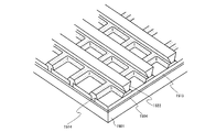
1514:隔壁
1515R、1515G、1515B:発光層を含む積層膜
1516:第2の電極
1521:発光領域
1522:逆テーパ状の隔壁
1601:第1の基板
1602:データ線
1603:走査線
1604:隔壁
1605:領域
1607:入力端子
1608:接続配線
1609a、1609b:FPC
1700 有機化合物を含む層
1701 ソース側駆動回路
1702 画素部
1703 ゲート側駆動回路
1704 封止基板
1705 シール材
1707 空間
1709 FPC(フレキシブルプリントサーキット)
1710 素子基板
1711 スイッチング用TFT
1712 電流制御用TFT
1713 陽極
1714 絶縁物
1715 発光素子
1716 陰極
1723 nチャネル型TFT
1724 pチャネル型TFT
8001 筐体
8002 支持台
8003 表示部
8004 スピーカー部
8005 ビデオ入力端子
8101 本体
8102 筐体
8103 表示部
8104 キーボード
8105 外部接続ポート
8106 マウス
8201 本体
8202 表示部
8203 筐体
8204 外部接続ポート
8205 リモコン受信部
8206 受像部
8207 バッテリー
8208 音声入力部
8209 操作キー
8301 照明部
8302 傘
8303 可変アーム
8304 支柱
8305 台
8306 電源
8401 本体
8402 筐体
8403 表示部
8404 音声入力部
8405 音声出力部
8406 操作キー
8407 外部接続ポート
8408 アンテナ
9501 車体
9502 表示パネル
Claims (8)
- レーザ光を射出する光源ユニットと、
前記レーザ光を矩形状または線状のレーザビームに成形する光学系と、
前記矩形状または線状のレーザビームを選択的に遮光または反射する光制御手段と、
前記光制御手段を通過したレーザビームを被照射基板に設けられた光吸収層上に走査する走査手段と、
前記光制御手段と、前記被照射基板と、被成膜基板との位置あわせを行うアライメント手段とを有し、
前記光制御手段を通過したレーザビームは、前記光吸収層を加熱し、前記光吸収層が前記被照射基板に設けられた第1の材料層を加熱し、前記第1の材料層の少なくとも一部を気化させ、前記被照射基板に対向して配置された前記被成膜基板上に第2の材料層を形成する製造装置。 - レーザ光を射出する光源ユニットと、
前記レーザ光を矩形状または線状のレーザビームに成形する光学系と、
前記矩形状または線状のレーザビームを選択的に遮光または反射する光制御手段と、
前記光制御手段を通過したレーザビームを被照射基板に設けられたガスを発生する層上に走査する走査手段と、
前記光制御手段と、前記ガスを発生する層及び第1の材料層が積層された被照射基板と、被成膜基板との位置あわせを行うアライメント手段とを有し、
前記光制御手段を通過したレーザビームは、前記被照射基板に設けられた前記ガスを発生する層を加熱し、前記ガスを発生する層を気化させ、前記被照射基板に対向して配置された前記被成膜基板上に第2の材料層を形成する製造装置。 - 請求項1または請求項2において、さらに前記光源ユニット、前記光制御手段、及び前記走査手段を制御する制御装置を備えている製造装置。
- 請求項1乃至3のいずれか一において、前記矩形状または線状のレーザビームの長辺方向は、前記走査手段で走査する方向と直交する製造装置。
- 請求項1乃至4のいずれか一において、前記被照射基板は、透光性を有する基板である製造装置。
- 請求項1乃至5のいずれか一において、前記光制御手段は、フォトマスク、スリット、またはメタルマスクである製造装置。
- 被照射基板の一方の面上に光の照射によりガスを発生する層を形成し、
前記ガスを発生する層上に材料層を形成し、
被成膜基板の一方の面を前記被照射基板の一方の面と対向させて配置し、
前記被照射基板のもう一方の面を通過させて光を前記ガスを発生する層に照射して、前記被成膜基板の一方の面上に材料層を成膜する発光装置の作製方法。 - 請求項7において、前記光は、レーザ光、放電灯、または発熱灯である発光装置の作製方法。
Priority Applications (1)
| Application Number | Priority Date | Filing Date | Title |
|---|---|---|---|
| JP2008137564A JP2009009935A (ja) | 2007-06-01 | 2008-05-27 | 製造装置および発光装置の作製方法 |
Applications Claiming Priority (2)
| Application Number | Priority Date | Filing Date | Title |
|---|---|---|---|
| JP2007147413 | 2007-06-01 | ||
| JP2008137564A JP2009009935A (ja) | 2007-06-01 | 2008-05-27 | 製造装置および発光装置の作製方法 |
Related Child Applications (1)
| Application Number | Title | Priority Date | Filing Date |
|---|---|---|---|
| JP2013021283A Division JP2013127977A (ja) | 2007-06-01 | 2013-02-06 | 発光装置の作製方法及び発光装置 |
Publications (2)
| Publication Number | Publication Date |
|---|---|
| JP2009009935A true JP2009009935A (ja) | 2009-01-15 |
| JP2009009935A5 JP2009009935A5 (ja) | 2011-06-16 |
Family
ID=40088662
Family Applications (3)
| Application Number | Title | Priority Date | Filing Date |
|---|---|---|---|
| JP2008137564A Withdrawn JP2009009935A (ja) | 2007-06-01 | 2008-05-27 | 製造装置および発光装置の作製方法 |
| JP2013021283A Withdrawn JP2013127977A (ja) | 2007-06-01 | 2013-02-06 | 発光装置の作製方法及び発光装置 |
| JP2015001480A Expired - Fee Related JP5957098B2 (ja) | 2007-06-01 | 2015-01-07 | 発光装置の作製方法 |
Family Applications After (2)
| Application Number | Title | Priority Date | Filing Date |
|---|---|---|---|
| JP2013021283A Withdrawn JP2013127977A (ja) | 2007-06-01 | 2013-02-06 | 発光装置の作製方法及び発光装置 |
| JP2015001480A Expired - Fee Related JP5957098B2 (ja) | 2007-06-01 | 2015-01-07 | 発光装置の作製方法 |
Country Status (4)
| Country | Link |
|---|---|
| US (2) | US8232038B2 (ja) |
| JP (3) | JP2009009935A (ja) |
| KR (1) | KR101563237B1 (ja) |
| CN (1) | CN101314841B (ja) |
Cited By (6)
| Publication number | Priority date | Publication date | Assignee | Title |
|---|---|---|---|---|
| EP2110540A2 (en) | 2008-04-15 | 2009-10-21 | Denso Corporation | Fuel injector with fuel pressure sensor |
| JP2011023731A (ja) * | 2009-09-15 | 2011-02-03 | Von Ardenne Anlagentechnik Gmbh | 微細構造を製造するための方法及び装置 |
| WO2012133203A1 (ja) * | 2011-03-30 | 2012-10-04 | シャープ株式会社 | 蒸着膜パターンの形成方法および有機エレクトロルミネッセンス表示装置の製造方法 |
| JP2013016480A (ja) * | 2011-06-30 | 2013-01-24 | Samsung Display Co Ltd | レーザー熱転写装置及びこれを用いた有機発光表示装置の製造方法 |
| JP2013073822A (ja) * | 2011-09-28 | 2013-04-22 | Ulvac Japan Ltd | 転写成膜装置 |
| JP2019023739A (ja) * | 2013-12-02 | 2019-02-14 | 株式会社半導体エネルギー研究所 | 装置 |
Families Citing this family (39)
| Publication number | Priority date | Publication date | Assignee | Title |
|---|---|---|---|---|
| US8080811B2 (en) | 2007-12-28 | 2011-12-20 | Semiconductor Energy Laboratory Co., Ltd. | Method for manufacturing evaporation donor substrate and light-emitting device |
| WO2009099002A1 (en) * | 2008-02-04 | 2009-08-13 | Semiconductor Energy Laboratory Co., Ltd. | Deposition method and method for manufacturing light-emitting device |
| WO2009107548A1 (en) * | 2008-02-29 | 2009-09-03 | Semiconductor Energy Laboratory Co., Ltd. | Deposition method and manufacturing method of light-emitting device |
| JP5416987B2 (ja) * | 2008-02-29 | 2014-02-12 | 株式会社半導体エネルギー研究所 | 成膜方法及び発光装置の作製方法 |
| US20090218219A1 (en) * | 2008-02-29 | 2009-09-03 | Semiconductor Energy Laboratory Co., Ltd. | Manufacturing Apparatus |
| JP5238544B2 (ja) * | 2008-03-07 | 2013-07-17 | 株式会社半導体エネルギー研究所 | 成膜方法及び発光装置の作製方法 |
| JP5079722B2 (ja) | 2008-03-07 | 2012-11-21 | 株式会社半導体エネルギー研究所 | 発光装置の作製方法 |
| US8182863B2 (en) * | 2008-03-17 | 2012-05-22 | Semiconductor Energy Laboratory Co., Ltd. | Deposition method and manufacturing method of light-emitting device |
| US7993945B2 (en) * | 2008-04-11 | 2011-08-09 | Semiconductor Energy Laboratory Co., Ltd. | Method for manufacturing light-emitting device |
| JP5244680B2 (ja) * | 2008-04-14 | 2013-07-24 | 株式会社半導体エネルギー研究所 | 発光装置の作製方法 |
| US8409672B2 (en) * | 2008-04-24 | 2013-04-02 | Semiconductor Energy Laboratory Co., Ltd. | Method of manufacturing evaporation donor substrate and method of manufacturing light-emitting device |
| JP5159689B2 (ja) * | 2008-04-25 | 2013-03-06 | 株式会社半導体エネルギー研究所 | 発光装置の作製方法 |
| KR101629637B1 (ko) * | 2008-05-29 | 2016-06-13 | 가부시키가이샤 한도오따이 에네루기 켄큐쇼 | 성막방법 및 발광장치의 제조방법 |
| US7919340B2 (en) * | 2008-06-04 | 2011-04-05 | Semiconductor Energy Laboratory Co., Ltd. | Method for manufacturing light-emitting device |
| US8574709B2 (en) * | 2008-07-21 | 2013-11-05 | Semiconductor Energy Laboratory Co., Ltd. | Deposition donor substrate and method for manufacturing light-emitting device |
| JP5469950B2 (ja) * | 2008-08-08 | 2014-04-16 | 株式会社半導体エネルギー研究所 | 発光装置の作製方法 |
| US8486736B2 (en) * | 2008-10-20 | 2013-07-16 | Semiconductor Energy Laboratory Co., Ltd. | Method for manufacturing light-emitting device |
| JP5291607B2 (ja) * | 2008-12-15 | 2013-09-18 | 株式会社半導体エネルギー研究所 | 発光装置の作製方法 |
| KR101023133B1 (ko) * | 2009-03-19 | 2011-03-18 | 삼성모바일디스플레이주식회사 | 유기 발광 표시 장치 |
| JP2012124478A (ja) * | 2010-11-19 | 2012-06-28 | Semiconductor Energy Lab Co Ltd | 照明装置 |
| KR101328979B1 (ko) * | 2011-06-30 | 2013-11-13 | 삼성디스플레이 주식회사 | 유기 발광 표시장치 |
| KR101787450B1 (ko) * | 2011-08-09 | 2017-10-19 | 삼성디스플레이 주식회사 | 표시 장치 |
| EP2591875B1 (de) * | 2011-11-09 | 2017-01-25 | Leister Technologies AG | Laser mit Strahltransformationslinse |
| KR101959975B1 (ko) * | 2012-07-10 | 2019-07-16 | 삼성디스플레이 주식회사 | 유기층 증착 장치, 이를 이용한 유기 발광 디스플레이 장치의 제조 방법 및 이에 따라 제조된 유기 발광 디스플레이 장치 |
| EP2731126A1 (en) | 2012-11-09 | 2014-05-14 | Nederlandse Organisatie voor toegepast -natuurwetenschappelijk onderzoek TNO | Method for bonding bare chip dies |
| CN104752469B (zh) * | 2013-12-31 | 2018-08-03 | 昆山国显光电有限公司 | 一种像素结构及采用该像素结构的有机发光显示器 |
| FR3025936B1 (fr) * | 2014-09-11 | 2016-12-02 | Saint Gobain | Procede de recuit par lampes flash |
| CN105679967B (zh) * | 2014-11-18 | 2018-06-26 | 昆山国显光电有限公司 | 掩膜板、制备有机发光显示装置的方法 |
| CN104795425A (zh) * | 2015-03-30 | 2015-07-22 | 京东方科技集团股份有限公司 | 有机发光二极管触控显示屏及其制作方法 |
| KR102388724B1 (ko) * | 2015-08-21 | 2022-04-21 | 삼성디스플레이 주식회사 | 증착용 마스크 제조 방법 |
| KR102404575B1 (ko) | 2015-10-12 | 2022-06-03 | 삼성디스플레이 주식회사 | 증착 장치와 이를 이용한 유기 발광 디스플레이 장치의 제조 방법 |
| JP7020896B2 (ja) * | 2017-12-14 | 2022-02-16 | 株式会社キーエンス | レーザ加工装置 |
| US10138539B1 (en) * | 2018-04-03 | 2018-11-27 | Shiping Cheng | Method of managing coating uniformity with an optical thickness monitoring system |
| US11094530B2 (en) | 2019-05-14 | 2021-08-17 | Applied Materials, Inc. | In-situ curing of color conversion layer |
| US11239213B2 (en) * | 2019-05-17 | 2022-02-01 | Applied Materials, Inc. | In-situ curing of color conversion layer in recess |
| JP2023535069A (ja) | 2020-07-24 | 2023-08-15 | アプライド マテリアルズ インコーポレイテッド | Uv-led硬化用の、チオール系架橋剤を有する量子ドット調製物 |
| CN112002712B (zh) * | 2020-08-24 | 2022-09-16 | 武汉天马微电子有限公司 | 一种显示面板、显示装置及制作方法 |
| US11646397B2 (en) | 2020-08-28 | 2023-05-09 | Applied Materials, Inc. | Chelating agents for quantum dot precursor materials in color conversion layers for micro-LEDs |
| CN113770546A (zh) * | 2021-10-11 | 2021-12-10 | 上海莘芝光电科技有限公司东莞分公司 | 一种通过激光蚀刻和碳化塑料表面制作立体线路的工艺 |
Citations (10)
| Publication number | Priority date | Publication date | Assignee | Title |
|---|---|---|---|---|
| WO2003010825A1 (en) * | 2001-07-24 | 2003-02-06 | Seiko Epson Corporation | Transfer method, method of manufacturing thin film element, method of manufacturing integrated circuit, circuit substrate and method of manufacturing the circuit substrate, electro-optic device and method of manufacturing the electro-optic device, and ic card and electronic equipmen |
| JP2004071551A (ja) * | 2002-08-02 | 2004-03-04 | Eastman Kodak Co | ドナー要素及びその使用方法 |
| JP2004220852A (ja) * | 2003-01-10 | 2004-08-05 | Sony Corp | 成膜装置および有機el素子の製造装置 |
| JP2005081299A (ja) * | 2003-09-10 | 2005-03-31 | Seiko Epson Corp | 成膜方法、配線パターンの形成方法、半導体装置の製造方法、電気光学装置、及び電子機器 |
| WO2005119804A2 (en) * | 2004-05-27 | 2005-12-15 | Eastman Kodak Company | Depositing organic layers for oled |
| JP2006073521A (ja) * | 2004-08-30 | 2006-03-16 | Samsung Sdi Co Ltd | レーザ転写用ドナー基板及びこの基板を使用して製造される有機電界発光素子の製造方法 |
| JP2006114470A (ja) * | 2004-10-15 | 2006-04-27 | Samsung Sdi Co Ltd | 有機電界発光素子 |
| JP2006231407A (ja) * | 2005-02-22 | 2006-09-07 | Samsung Sdi Co Ltd | レーザ照射装置及びレーザ熱転写法 |
| JP2006302636A (ja) * | 2005-04-20 | 2006-11-02 | Konica Minolta Holdings Inc | 有機エレクトロルミネッセンス素子、有機エレクトロルミネッセンス素子の製造方法、表示装置および照明装置 |
| JP2006344459A (ja) * | 2005-06-08 | 2006-12-21 | Sony Corp | 転写方法および転写装置 |
Family Cites Families (50)
| Publication number | Priority date | Publication date | Assignee | Title |
|---|---|---|---|---|
| US5356853A (en) * | 1990-09-07 | 1994-10-18 | Dai Nippon Printing Co., Ltd. | Thermal transfer image receiving sheet, production process therefor and thermal transfer sheet |
| JPH0911646A (ja) * | 1995-06-30 | 1997-01-14 | Fuji Photo Film Co Ltd | 熱転写シート |
| US6372608B1 (en) * | 1996-08-27 | 2002-04-16 | Seiko Epson Corporation | Separating method, method for transferring thin film device, thin film device, thin film integrated circuit device, and liquid crystal display device manufactured by using the transferring method |
| JP3801730B2 (ja) | 1997-05-09 | 2006-07-26 | 株式会社半導体エネルギー研究所 | プラズマcvd装置及びそれを用いた薄膜形成方法 |
| US5937272A (en) | 1997-06-06 | 1999-08-10 | Eastman Kodak Company | Patterned organic layers in a full-color organic electroluminescent display array on a thin film transistor array substrate |
| JPH1126733A (ja) * | 1997-07-03 | 1999-01-29 | Seiko Epson Corp | 薄膜デバイスの転写方法、薄膜デバイス、薄膜集積回路装置,アクティブマトリクス基板、液晶表示装置および電子機器 |
| TW495635B (en) * | 1997-07-11 | 2002-07-21 | Hitachi Ltd | Liquid crystal display device |
| US6165543A (en) | 1998-06-17 | 2000-12-26 | Nec Corporation | Method of making organic EL device and organic EL transfer base plate |
| ES2149637T3 (es) * | 1999-01-28 | 2000-11-01 | Leister Process Tech | Procedimiento de ensamblaje por laser y dispositivo para unir distintas piezas de plastico o plastico con otros materiales. |
| JP3740557B2 (ja) | 1999-03-09 | 2006-02-01 | 独立行政法人産業技術総合研究所 | 有機薄膜作製方法および有機薄膜作製装置 |
| TW527735B (en) | 1999-06-04 | 2003-04-11 | Semiconductor Energy Lab | Electro-optical device |
| US8853696B1 (en) | 1999-06-04 | 2014-10-07 | Semiconductor Energy Laboratory Co., Ltd. | Electro-optical device and electronic device |
| TW501379B (en) * | 2000-07-25 | 2002-09-01 | Eastman Kodak Co | Method of making organic electroluminescent device using laser transfer |
| US6495405B2 (en) * | 2001-01-29 | 2002-12-17 | Sharp Laboratories Of America, Inc. | Method of optimizing channel characteristics using laterally-crystallized ELA poly-Si films |
| US6719916B2 (en) * | 2001-04-18 | 2004-04-13 | National Research Council Of Canada | Multilayer microstructures and laser based method for precision and reduced damage patterning of such structures |
| WO2002096667A1 (fr) * | 2001-05-28 | 2002-12-05 | Fuji Photo Film Co., Ltd. | Procede d'enregistrement par transfert thermique par laser |
| JP2002367777A (ja) * | 2001-06-07 | 2002-12-20 | Sharp Corp | 有機エレクトロルミネッセンス素子の製造方法 |
| SG149680A1 (en) | 2001-12-12 | 2009-02-27 | Semiconductor Energy Lab | Film formation apparatus and film formation method and cleaning method |
| JP4294305B2 (ja) | 2001-12-12 | 2009-07-08 | 株式会社半導体エネルギー研究所 | 成膜装置および成膜方法 |
| US6582875B1 (en) * | 2002-01-23 | 2003-06-24 | Eastman Kodak Company | Using a multichannel linear laser light beam in making OLED devices by thermal transfer |
| JP2003264076A (ja) | 2002-03-08 | 2003-09-19 | Sharp Corp | 有機発光層形成用塗液、有機led用ドナーフィルム、それを用いた有機led表示パネルの製造方法および有機led表示パネル |
| US6703179B2 (en) | 2002-03-13 | 2004-03-09 | Eastman Kodak Company | Transfer of organic material from a donor to form a layer in an OLED device |
| JP2003347192A (ja) * | 2002-05-24 | 2003-12-05 | Toshiba Corp | エネルギービーム露光方法および露光装置 |
| GB0213695D0 (en) * | 2002-06-14 | 2002-07-24 | Filtronic Compound Semiconduct | Fabrication method |
| JP2004022400A (ja) * | 2002-06-18 | 2004-01-22 | Sony Corp | 有機膜形成装置および有機膜形成方法 |
| JP2004103406A (ja) | 2002-09-10 | 2004-04-02 | Sony Corp | 薄膜パターン形成方法および装置並びに有機el表示装置の製造方法 |
| US7136084B2 (en) * | 2002-09-17 | 2006-11-14 | Miller Timothy J | Random laser image projector system and method |
| US20040191564A1 (en) * | 2002-12-17 | 2004-09-30 | Samsung Sdi Co., Ltd. | Donor film for low molecular weight full color organic electroluminescent device using laser induced thermal imaging method and method for fabricating low molecular weight full color organic electroluminescent device using the film |
| US7220627B2 (en) * | 2003-04-21 | 2007-05-22 | Semiconductor Energy Laboratory Co., Ltd. | Method for manufacturing a semiconductor device where the scanning direction changes between regions during crystallization and process |
| JP4493926B2 (ja) | 2003-04-25 | 2010-06-30 | 株式会社半導体エネルギー研究所 | 製造装置 |
| JP4179041B2 (ja) * | 2003-04-30 | 2008-11-12 | 株式会社島津製作所 | 有機el用保護膜の成膜装置、製造方法および有機el素子 |
| JP2004335649A (ja) * | 2003-05-06 | 2004-11-25 | Seiko Epson Corp | 露光装置及び露光方法、露光用マスク、半導体装置 |
| EP1491653A3 (en) | 2003-06-13 | 2005-06-15 | Pioneer Corporation | Evaporative deposition methods and apparatus |
| JP4433722B2 (ja) * | 2003-08-12 | 2010-03-17 | セイコーエプソン株式会社 | パターンの形成方法及び配線パターンの形成方法 |
| JP4402440B2 (ja) * | 2003-12-03 | 2010-01-20 | 大日本印刷株式会社 | カラーフィルタおよびカラーフィルタの製造方法 |
| US20050145326A1 (en) | 2004-01-05 | 2005-07-07 | Eastman Kodak Company | Method of making an OLED device |
| JP2005249937A (ja) * | 2004-03-02 | 2005-09-15 | Dainippon Printing Co Ltd | カラーフィルタの製造方法及び装置 |
| JP4754848B2 (ja) * | 2004-03-03 | 2011-08-24 | 株式会社半導体エネルギー研究所 | 半導体装置の作製方法 |
| KR101066478B1 (ko) * | 2004-06-04 | 2011-09-21 | 엘지디스플레이 주식회사 | 레이저 빔 패턴 마스크 및 이를 이용한 결정화 방법 |
| US7744770B2 (en) * | 2004-06-23 | 2010-06-29 | Sony Corporation | Device transfer method |
| JP4545504B2 (ja) * | 2004-07-15 | 2010-09-15 | 株式会社半導体エネルギー研究所 | 膜形成方法、発光装置の作製方法 |
| JP2006120726A (ja) * | 2004-10-19 | 2006-05-11 | Seiko Epson Corp | 薄膜装置の製造方法、電気光学装置、及び電子機器 |
| JP4793071B2 (ja) * | 2005-04-18 | 2011-10-12 | ソニー株式会社 | 表示装置および表示装置の製造方法 |
| JP2006309994A (ja) * | 2005-04-27 | 2006-11-09 | Sony Corp | 転写用基板および転写方法ならびに表示装置の製造方法 |
| JP2006309995A (ja) * | 2005-04-27 | 2006-11-09 | Sony Corp | 転写用基板および表示装置の製造方法ならびに表示装置 |
| TWI307612B (en) | 2005-04-27 | 2009-03-11 | Sony Corp | Transfer method and transfer apparatus |
| KR100645534B1 (ko) * | 2005-08-12 | 2006-11-14 | 삼성에스디아이 주식회사 | 레이저 열전사용 마스크 및 그를 이용한 유기 전계 발광소자의 제조방법 |
| EP1770443B1 (en) * | 2005-09-28 | 2016-01-20 | Semiconductor Energy Laboratory Co., Ltd. | Laser processing apparatus and exposure method |
| WO2008069259A1 (en) | 2006-12-05 | 2008-06-12 | Semiconductor Energy Laboratory Co., Ltd. | Film formation apparatus, film formation method, manufacturing apparatus, and method for manufacturing light-emitting device |
| JP5416987B2 (ja) | 2008-02-29 | 2014-02-12 | 株式会社半導体エネルギー研究所 | 成膜方法及び発光装置の作製方法 |
-
2008
- 2008-05-08 KR KR1020080042914A patent/KR101563237B1/ko active IP Right Grant
- 2008-05-20 US US12/123,902 patent/US8232038B2/en not_active Expired - Fee Related
- 2008-05-27 JP JP2008137564A patent/JP2009009935A/ja not_active Withdrawn
- 2008-05-29 CN CN2008100999941A patent/CN101314841B/zh not_active Expired - Fee Related
-
2012
- 2012-07-26 US US13/558,809 patent/US20120285379A1/en not_active Abandoned
-
2013
- 2013-02-06 JP JP2013021283A patent/JP2013127977A/ja not_active Withdrawn
-
2015
- 2015-01-07 JP JP2015001480A patent/JP5957098B2/ja not_active Expired - Fee Related
Patent Citations (10)
| Publication number | Priority date | Publication date | Assignee | Title |
|---|---|---|---|---|
| WO2003010825A1 (en) * | 2001-07-24 | 2003-02-06 | Seiko Epson Corporation | Transfer method, method of manufacturing thin film element, method of manufacturing integrated circuit, circuit substrate and method of manufacturing the circuit substrate, electro-optic device and method of manufacturing the electro-optic device, and ic card and electronic equipmen |
| JP2004071551A (ja) * | 2002-08-02 | 2004-03-04 | Eastman Kodak Co | ドナー要素及びその使用方法 |
| JP2004220852A (ja) * | 2003-01-10 | 2004-08-05 | Sony Corp | 成膜装置および有機el素子の製造装置 |
| JP2005081299A (ja) * | 2003-09-10 | 2005-03-31 | Seiko Epson Corp | 成膜方法、配線パターンの形成方法、半導体装置の製造方法、電気光学装置、及び電子機器 |
| WO2005119804A2 (en) * | 2004-05-27 | 2005-12-15 | Eastman Kodak Company | Depositing organic layers for oled |
| JP2006073521A (ja) * | 2004-08-30 | 2006-03-16 | Samsung Sdi Co Ltd | レーザ転写用ドナー基板及びこの基板を使用して製造される有機電界発光素子の製造方法 |
| JP2006114470A (ja) * | 2004-10-15 | 2006-04-27 | Samsung Sdi Co Ltd | 有機電界発光素子 |
| JP2006231407A (ja) * | 2005-02-22 | 2006-09-07 | Samsung Sdi Co Ltd | レーザ照射装置及びレーザ熱転写法 |
| JP2006302636A (ja) * | 2005-04-20 | 2006-11-02 | Konica Minolta Holdings Inc | 有機エレクトロルミネッセンス素子、有機エレクトロルミネッセンス素子の製造方法、表示装置および照明装置 |
| JP2006344459A (ja) * | 2005-06-08 | 2006-12-21 | Sony Corp | 転写方法および転写装置 |
Cited By (16)
| Publication number | Priority date | Publication date | Assignee | Title |
|---|---|---|---|---|
| EP2110540A2 (en) | 2008-04-15 | 2009-10-21 | Denso Corporation | Fuel injector with fuel pressure sensor |
| JP2011023731A (ja) * | 2009-09-15 | 2011-02-03 | Von Ardenne Anlagentechnik Gmbh | 微細構造を製造するための方法及び装置 |
| WO2012133203A1 (ja) * | 2011-03-30 | 2012-10-04 | シャープ株式会社 | 蒸着膜パターンの形成方法および有機エレクトロルミネッセンス表示装置の製造方法 |
| JP2013016480A (ja) * | 2011-06-30 | 2013-01-24 | Samsung Display Co Ltd | レーザー熱転写装置及びこれを用いた有機発光表示装置の製造方法 |
| US8842144B2 (en) | 2011-06-30 | 2014-09-23 | Samsung Display Co., Ltd. | Laser induced thermal imaging apparatus and method for manufacturing organic light emitting diode (OLED) display device using the same |
| JP2013073822A (ja) * | 2011-09-28 | 2013-04-22 | Ulvac Japan Ltd | 転写成膜装置 |
| US10355067B2 (en) | 2013-12-02 | 2019-07-16 | Semiconductor Energy Laboratory Co., Ltd. | Display device and method for manufacturing the same |
| US10312315B2 (en) | 2013-12-02 | 2019-06-04 | Semiconductor Energy Laboratory Co., Ltd. | Display device and method for manufacturing the same |
| JP2019023739A (ja) * | 2013-12-02 | 2019-02-14 | 株式会社半導体エネルギー研究所 | 装置 |
| US10763322B2 (en) | 2013-12-02 | 2020-09-01 | Semiconductor Energy Laboratory Co., Ltd. | Display device and method for manufacturing the same |
| JP2020166274A (ja) * | 2013-12-02 | 2020-10-08 | 株式会社半導体エネルギー研究所 | 線状ビーム照射装置 |
| US10854697B2 (en) | 2013-12-02 | 2020-12-01 | Semiconductor Energy Laboratory Co., Ltd. | Display device and method for manufacturing the same |
| US10872947B2 (en) | 2013-12-02 | 2020-12-22 | Semiconductor Energy Laboratory Co., Ltd. | Display device and method for manufacturing the same |
| US10879331B2 (en) | 2013-12-02 | 2020-12-29 | Semiconductor Energy Laboratory Co., Ltd. | Display device and method for manufacturing the same |
| US11004925B2 (en) | 2013-12-02 | 2021-05-11 | Semiconductor Energy Laboratory Co., Ltd. | Display device and method for manufacturing the same |
| US11672148B2 (en) | 2013-12-02 | 2023-06-06 | Semiconductor Energy Laboratory Co., Ltd. | Display device and method for manufacturing the same |
Also Published As
| Publication number | Publication date |
|---|---|
| US8232038B2 (en) | 2012-07-31 |
| US20120285379A1 (en) | 2012-11-15 |
| JP2015092504A (ja) | 2015-05-14 |
| US20080299496A1 (en) | 2008-12-04 |
| KR20080105998A (ko) | 2008-12-04 |
| KR101563237B1 (ko) | 2015-10-26 |
| CN101314841A (zh) | 2008-12-03 |
| JP5957098B2 (ja) | 2016-07-27 |
| JP2013127977A (ja) | 2013-06-27 |
| CN101314841B (zh) | 2013-06-12 |
Similar Documents
| Publication | Publication Date | Title |
|---|---|---|
| JP5957098B2 (ja) | 発光装置の作製方法 | |
| US10199612B2 (en) | Semiconductor device having reduced upper surface shape of a partition in order to improve definition and manufacturing method thereof | |
| US8367152B2 (en) | Manufacturing method of light-emitting device | |
| JP5190253B2 (ja) | 混合層の作製方法、発光装置の作製方法 | |
| TWI513075B (zh) | 發光裝置的製造方法 | |
| JP5165452B2 (ja) | 成膜方法及び発光装置の作製方法 | |
| TW200529445A (en) | Display device and method for fabricating the same | |
| JP4801347B2 (ja) | 表示装置 | |
| JP2008135717A (ja) | 半導体装置の作製方法およびレーザ加工装置 | |
| JP4884674B2 (ja) | 表示装置の作製方法 | |
| US8455337B2 (en) | Crystallization apparatus, crystallization method, method of manufacturing thin film transistor and method of manufacturing organic light emitting display apparatus |
Legal Events
| Date | Code | Title | Description |
|---|---|---|---|
| A521 | Request for written amendment filed |
Free format text: JAPANESE INTERMEDIATE CODE: A523 Effective date: 20110428 |
|
| A621 | Written request for application examination |
Free format text: JAPANESE INTERMEDIATE CODE: A621 Effective date: 20110428 |
|
| A131 | Notification of reasons for refusal |
Free format text: JAPANESE INTERMEDIATE CODE: A131 Effective date: 20120131 |
|
| A521 | Request for written amendment filed |
Free format text: JAPANESE INTERMEDIATE CODE: A523 Effective date: 20120327 |
|
| A131 | Notification of reasons for refusal |
Free format text: JAPANESE INTERMEDIATE CODE: A131 Effective date: 20120612 |
|
| A521 | Request for written amendment filed |
Free format text: JAPANESE INTERMEDIATE CODE: A523 Effective date: 20120724 |
|
| A131 | Notification of reasons for refusal |
Free format text: JAPANESE INTERMEDIATE CODE: A131 Effective date: 20120904 |
|
| A521 | Request for written amendment filed |
Free format text: JAPANESE INTERMEDIATE CODE: A523 Effective date: 20121003 |
|
| A02 | Decision of refusal |
Free format text: JAPANESE INTERMEDIATE CODE: A02 Effective date: 20121120 |
|
| A761 | Written withdrawal of application |
Free format text: JAPANESE INTERMEDIATE CODE: A761 Effective date: 20130212 |