US7919340B2 - Method for manufacturing light-emitting device - Google Patents
Method for manufacturing light-emitting device Download PDFInfo
- Publication number
- US7919340B2 US7919340B2 US12/476,556 US47655609A US7919340B2 US 7919340 B2 US7919340 B2 US 7919340B2 US 47655609 A US47655609 A US 47655609A US 7919340 B2 US7919340 B2 US 7919340B2
- Authority
- US
- United States
- Prior art keywords
- light
- substrate
- layer
- emitting device
- manufacturing
- Prior art date
- Legal status (The legal status is an assumption and is not a legal conclusion. Google has not performed a legal analysis and makes no representation as to the accuracy of the status listed.)
- Expired - Fee Related, expires
Links
- 238000000034 method Methods 0.000 title claims description 91
- 238000004519 manufacturing process Methods 0.000 title claims description 56
- 239000000758 substrate Substances 0.000 claims abstract description 358
- 239000000463 material Substances 0.000 claims abstract description 276
- 238000001704 evaporation Methods 0.000 claims abstract description 104
- 230000008021 deposition Effects 0.000 claims abstract description 78
- 230000031700 light absorption Effects 0.000 claims description 69
- 229910052782 aluminium Inorganic materials 0.000 claims description 20
- XAGFODPZIPBFFR-UHFFFAOYSA-N aluminium Chemical compound [Al] XAGFODPZIPBFFR-UHFFFAOYSA-N 0.000 claims description 20
- 239000000956 alloy Substances 0.000 claims description 19
- 229910045601 alloy Inorganic materials 0.000 claims description 19
- 229910052799 carbon Inorganic materials 0.000 claims description 17
- 229910052709 silver Inorganic materials 0.000 claims description 15
- 239000004332 silver Substances 0.000 claims description 15
- 238000010438 heat treatment Methods 0.000 claims description 14
- BASFCYQUMIYNBI-UHFFFAOYSA-N platinum Chemical compound [Pt] BASFCYQUMIYNBI-UHFFFAOYSA-N 0.000 claims description 13
- BQCADISMDOOEFD-UHFFFAOYSA-N Silver Chemical compound [Ag] BQCADISMDOOEFD-UHFFFAOYSA-N 0.000 claims description 12
- NRTOMJZYCJJWKI-UHFFFAOYSA-N Titanium nitride Chemical compound [Ti]#N NRTOMJZYCJJWKI-UHFFFAOYSA-N 0.000 claims description 9
- 150000002894 organic compounds Chemical class 0.000 claims description 9
- 230000001678 irradiating effect Effects 0.000 claims description 8
- 239000010949 copper Substances 0.000 claims description 7
- 239000010931 gold Substances 0.000 claims description 7
- AMGQUBHHOARCQH-UHFFFAOYSA-N indium;oxotin Chemical compound [In].[Sn]=O AMGQUBHHOARCQH-UHFFFAOYSA-N 0.000 claims description 7
- RYGMFSIKBFXOCR-UHFFFAOYSA-N Copper Chemical compound [Cu] RYGMFSIKBFXOCR-UHFFFAOYSA-N 0.000 claims description 6
- 229910052802 copper Inorganic materials 0.000 claims description 6
- PCHJSUWPFVWCPO-UHFFFAOYSA-N gold Chemical compound [Au] PCHJSUWPFVWCPO-UHFFFAOYSA-N 0.000 claims description 6
- 229910052737 gold Inorganic materials 0.000 claims description 6
- 229910052697 platinum Inorganic materials 0.000 claims description 6
- 239000010936 titanium Substances 0.000 claims description 6
- 229910052721 tungsten Inorganic materials 0.000 claims description 6
- 239000010937 tungsten Substances 0.000 claims description 6
- 229910052724 xenon Inorganic materials 0.000 claims description 6
- FHNFHKCVQCLJFQ-UHFFFAOYSA-N xenon atom Chemical compound [Xe] FHNFHKCVQCLJFQ-UHFFFAOYSA-N 0.000 claims description 6
- OKTJSMMVPCPJKN-UHFFFAOYSA-N Carbon Chemical compound [C] OKTJSMMVPCPJKN-UHFFFAOYSA-N 0.000 claims description 5
- SJKRCWUQJZIWQB-UHFFFAOYSA-N azane;chromium Chemical compound N.[Cr] SJKRCWUQJZIWQB-UHFFFAOYSA-N 0.000 claims description 5
- RRZKHZBOZDIQJG-UHFFFAOYSA-N azane;manganese Chemical compound N.[Mn] RRZKHZBOZDIQJG-UHFFFAOYSA-N 0.000 claims description 5
- 229910052736 halogen Inorganic materials 0.000 claims description 5
- 150000002367 halogens Chemical class 0.000 claims description 5
- MZLGASXMSKOWSE-UHFFFAOYSA-N tantalum nitride Chemical compound [Ta]#N MZLGASXMSKOWSE-UHFFFAOYSA-N 0.000 claims description 5
- WFKWXMTUELFFGS-UHFFFAOYSA-N tungsten Chemical compound [W] WFKWXMTUELFFGS-UHFFFAOYSA-N 0.000 claims description 5
- RTAQQCXQSZGOHL-UHFFFAOYSA-N Titanium Chemical compound [Ti] RTAQQCXQSZGOHL-UHFFFAOYSA-N 0.000 claims description 4
- 239000004411 aluminium Substances 0.000 claims description 4
- 229910001507 metal halide Inorganic materials 0.000 claims description 4
- 150000005309 metal halides Chemical class 0.000 claims description 4
- 229910052719 titanium Inorganic materials 0.000 claims description 4
- 229910052743 krypton Inorganic materials 0.000 claims description 3
- DNNSSWSSYDEUBZ-UHFFFAOYSA-N krypton atom Chemical compound [Kr] DNNSSWSSYDEUBZ-UHFFFAOYSA-N 0.000 claims description 3
- 230000008020 evaporation Effects 0.000 abstract description 97
- 230000006866 deterioration Effects 0.000 abstract description 11
- 239000010410 layer Substances 0.000 description 467
- 238000000151 deposition Methods 0.000 description 83
- 239000000126 substance Substances 0.000 description 61
- 239000010408 film Substances 0.000 description 47
- 239000012212 insulator Substances 0.000 description 17
- 230000006870 function Effects 0.000 description 16
- 238000012546 transfer Methods 0.000 description 16
- 150000001875 compounds Chemical class 0.000 description 13
- 239000011159 matrix material Substances 0.000 description 13
- 238000005192 partition Methods 0.000 description 13
- 230000001413 cellular effect Effects 0.000 description 11
- 229910052751 metal Inorganic materials 0.000 description 11
- 239000002184 metal Substances 0.000 description 11
- AZFHXIBNMPIGOD-UHFFFAOYSA-N 4-hydroxypent-3-en-2-one iridium Chemical compound [Ir].CC(O)=CC(C)=O.CC(O)=CC(C)=O.CC(O)=CC(C)=O AZFHXIBNMPIGOD-UHFFFAOYSA-N 0.000 description 10
- CUJRVFIICFDLGR-UHFFFAOYSA-N acetylacetonate Chemical compound CC(=O)[CH-]C(C)=O CUJRVFIICFDLGR-UHFFFAOYSA-N 0.000 description 10
- 230000015572 biosynthetic process Effects 0.000 description 10
- 239000002019 doping agent Substances 0.000 description 10
- 239000011521 glass Substances 0.000 description 10
- 239000000565 sealant Substances 0.000 description 10
- 230000003287 optical effect Effects 0.000 description 9
- 238000007789 sealing Methods 0.000 description 9
- VYPSYNLAJGMNEJ-UHFFFAOYSA-N silicon dioxide Inorganic materials O=[Si]=O VYPSYNLAJGMNEJ-UHFFFAOYSA-N 0.000 description 9
- -1 tungsten nitride Chemical class 0.000 description 9
- 239000007983 Tris buffer Substances 0.000 description 8
- XLOMVQKBTHCTTD-UHFFFAOYSA-N Zinc monoxide Chemical compound [Zn]=O XLOMVQKBTHCTTD-UHFFFAOYSA-N 0.000 description 8
- 229910044991 metal oxide Inorganic materials 0.000 description 8
- 150000004706 metal oxides Chemical class 0.000 description 8
- 239000002904 solvent Substances 0.000 description 8
- 238000004544 sputter deposition Methods 0.000 description 8
- 229910052784 alkaline earth metal Inorganic materials 0.000 description 6
- 150000001342 alkaline earth metals Chemical class 0.000 description 6
- 150000004945 aromatic hydrocarbons Chemical class 0.000 description 6
- 230000005281 excited state Effects 0.000 description 6
- MILUBEOXRNEUHS-UHFFFAOYSA-N iridium(3+) Chemical compound [Ir+3] MILUBEOXRNEUHS-UHFFFAOYSA-N 0.000 description 6
- 230000009467 reduction Effects 0.000 description 6
- 238000004088 simulation Methods 0.000 description 6
- 238000010521 absorption reaction Methods 0.000 description 5
- 229910052783 alkali metal Inorganic materials 0.000 description 5
- 150000001340 alkali metals Chemical class 0.000 description 5
- 239000011777 magnesium Substances 0.000 description 5
- 239000003550 marker Substances 0.000 description 5
- QGLKJKCYBOYXKC-UHFFFAOYSA-N nonaoxidotritungsten Chemical compound O=[W]1(=O)O[W](=O)(=O)O[W](=O)(=O)O1 QGLKJKCYBOYXKC-UHFFFAOYSA-N 0.000 description 5
- 230000008569 process Effects 0.000 description 5
- 239000010453 quartz Substances 0.000 description 5
- 239000002356 single layer Substances 0.000 description 5
- 238000000859 sublimation Methods 0.000 description 5
- 230000008022 sublimation Effects 0.000 description 5
- 229910001930 tungsten oxide Inorganic materials 0.000 description 5
- 238000001771 vacuum deposition Methods 0.000 description 5
- VFUDMQLBKNMONU-UHFFFAOYSA-N 9-[4-(4-carbazol-9-ylphenyl)phenyl]carbazole Chemical group C12=CC=CC=C2C2=CC=CC=C2N1C1=CC=C(C=2C=CC(=CC=2)N2C3=CC=CC=C3C3=CC=CC=C32)C=C1 VFUDMQLBKNMONU-UHFFFAOYSA-N 0.000 description 4
- XJHCXCQVJFPJIK-UHFFFAOYSA-M caesium fluoride Chemical compound [F-].[Cs+] XJHCXCQVJFPJIK-UHFFFAOYSA-M 0.000 description 4
- 238000006243 chemical reaction Methods 0.000 description 4
- 238000005137 deposition process Methods 0.000 description 4
- 239000002274 desiccant Substances 0.000 description 4
- 239000007850 fluorescent dye Substances 0.000 description 4
- AMWRITDGCCNYAT-UHFFFAOYSA-L hydroxy(oxo)manganese;manganese Chemical compound [Mn].O[Mn]=O.O[Mn]=O AMWRITDGCCNYAT-UHFFFAOYSA-L 0.000 description 4
- 229910003437 indium oxide Inorganic materials 0.000 description 4
- PJXISJQVUVHSOJ-UHFFFAOYSA-N indium(iii) oxide Chemical compound [O-2].[O-2].[O-2].[In+3].[In+3] PJXISJQVUVHSOJ-UHFFFAOYSA-N 0.000 description 4
- 229910010272 inorganic material Inorganic materials 0.000 description 4
- 229910000476 molybdenum oxide Inorganic materials 0.000 description 4
- PQQKPALAQIIWST-UHFFFAOYSA-N oxomolybdenum Chemical compound [Mo]=O PQQKPALAQIIWST-UHFFFAOYSA-N 0.000 description 4
- 238000012545 processing Methods 0.000 description 4
- 229910052761 rare earth metal Inorganic materials 0.000 description 4
- 239000011787 zinc oxide Substances 0.000 description 4
- IYZMXHQDXZKNCY-UHFFFAOYSA-N 1-n,1-n-diphenyl-4-n,4-n-bis[4-(n-phenylanilino)phenyl]benzene-1,4-diamine Chemical compound C1=CC=CC=C1N(C=1C=CC(=CC=1)N(C=1C=CC(=CC=1)N(C=1C=CC=CC=1)C=1C=CC=CC=1)C=1C=CC(=CC=1)N(C=1C=CC=CC=1)C=1C=CC=CC=1)C1=CC=CC=C1 IYZMXHQDXZKNCY-UHFFFAOYSA-N 0.000 description 3
- ZWEHNKRNPOVVGH-UHFFFAOYSA-N 2-Butanone Chemical compound CCC(C)=O ZWEHNKRNPOVVGH-UHFFFAOYSA-N 0.000 description 3
- CSCPPACGZOOCGX-UHFFFAOYSA-N Acetone Chemical compound CC(C)=O CSCPPACGZOOCGX-UHFFFAOYSA-N 0.000 description 3
- UHOVQNZJYSORNB-UHFFFAOYSA-N Benzene Chemical compound C1=CC=CC=C1 UHOVQNZJYSORNB-UHFFFAOYSA-N 0.000 description 3
- YMWUJEATGCHHMB-UHFFFAOYSA-N Dichloromethane Chemical compound ClCCl YMWUJEATGCHHMB-UHFFFAOYSA-N 0.000 description 3
- XEKOWRVHYACXOJ-UHFFFAOYSA-N Ethyl acetate Chemical compound CCOC(C)=O XEKOWRVHYACXOJ-UHFFFAOYSA-N 0.000 description 3
- 229910052693 Europium Inorganic materials 0.000 description 3
- FYYHWMGAXLPEAU-UHFFFAOYSA-N Magnesium Chemical compound [Mg] FYYHWMGAXLPEAU-UHFFFAOYSA-N 0.000 description 3
- ZOKXTWBITQBERF-UHFFFAOYSA-N Molybdenum Chemical compound [Mo] ZOKXTWBITQBERF-UHFFFAOYSA-N 0.000 description 3
- ZMXDDKWLCZADIW-UHFFFAOYSA-N N,N-Dimethylformamide Chemical compound CN(C)C=O ZMXDDKWLCZADIW-UHFFFAOYSA-N 0.000 description 3
- PXHVJJICTQNCMI-UHFFFAOYSA-N Nickel Chemical compound [Ni] PXHVJJICTQNCMI-UHFFFAOYSA-N 0.000 description 3
- KDLHZDBZIXYQEI-UHFFFAOYSA-N Palladium Chemical compound [Pd] KDLHZDBZIXYQEI-UHFFFAOYSA-N 0.000 description 3
- YNPNZTXNASCQKK-UHFFFAOYSA-N Phenanthrene Natural products C1=CC=C2C3=CC=CC=C3C=CC2=C1 YNPNZTXNASCQKK-UHFFFAOYSA-N 0.000 description 3
- XUIMIQQOPSSXEZ-UHFFFAOYSA-N Silicon Chemical compound [Si] XUIMIQQOPSSXEZ-UHFFFAOYSA-N 0.000 description 3
- YXFVVABEGXRONW-UHFFFAOYSA-N Toluene Chemical compound CC1=CC=CC=C1 YXFVVABEGXRONW-UHFFFAOYSA-N 0.000 description 3
- DGEZNRSVGBDHLK-UHFFFAOYSA-N [1,10]phenanthroline Chemical compound C1=CN=C2C3=NC=CC=C3C=CC2=C1 DGEZNRSVGBDHLK-UHFFFAOYSA-N 0.000 description 3
- 239000002585 base Substances 0.000 description 3
- 150000001716 carbazoles Chemical class 0.000 description 3
- 239000011651 chromium Substances 0.000 description 3
- 239000003086 colorant Substances 0.000 description 3
- 238000001816 cooling Methods 0.000 description 3
- 238000005566 electron beam evaporation Methods 0.000 description 3
- OGPBJKLSAFTDLK-UHFFFAOYSA-N europium atom Chemical compound [Eu] OGPBJKLSAFTDLK-UHFFFAOYSA-N 0.000 description 3
- 230000001747 exhibiting effect Effects 0.000 description 3
- 230000005283 ground state Effects 0.000 description 3
- 230000006872 improvement Effects 0.000 description 3
- 150000002484 inorganic compounds Chemical class 0.000 description 3
- 229910052749 magnesium Inorganic materials 0.000 description 3
- 150000002739 metals Chemical class 0.000 description 3
- 239000000203 mixture Substances 0.000 description 3
- 229910052750 molybdenum Inorganic materials 0.000 description 3
- 239000011733 molybdenum Substances 0.000 description 3
- VLKZOEOYAKHREP-UHFFFAOYSA-N n-Hexane Chemical compound CCCCCC VLKZOEOYAKHREP-UHFFFAOYSA-N 0.000 description 3
- IBHBKWKFFTZAHE-UHFFFAOYSA-N n-[4-[4-(n-naphthalen-1-ylanilino)phenyl]phenyl]-n-phenylnaphthalen-1-amine Chemical group C1=CC=CC=C1N(C=1C2=CC=CC=C2C=CC=1)C1=CC=C(C=2C=CC(=CC=2)N(C=2C=CC=CC=2)C=2C3=CC=CC=C3C=CC=2)C=C1 IBHBKWKFFTZAHE-UHFFFAOYSA-N 0.000 description 3
- 150000004767 nitrides Chemical class 0.000 description 3
- 239000004033 plastic Substances 0.000 description 3
- 229920003023 plastic Polymers 0.000 description 3
- 150000002910 rare earth metals Chemical class 0.000 description 3
- 230000007261 regionalization Effects 0.000 description 3
- 229910052710 silicon Inorganic materials 0.000 description 3
- 239000010703 silicon Substances 0.000 description 3
- 229910052814 silicon oxide Inorganic materials 0.000 description 3
- 238000004528 spin coating Methods 0.000 description 3
- ODHXBMXNKOYIBV-UHFFFAOYSA-N triphenylamine Chemical compound C1=CC=CC=C1N(C=1C=CC=CC=1)C1=CC=CC=C1 ODHXBMXNKOYIBV-UHFFFAOYSA-N 0.000 description 3
- UHXOHPVVEHBKKT-UHFFFAOYSA-N 1-(2,2-diphenylethenyl)-4-[4-(2,2-diphenylethenyl)phenyl]benzene Chemical group C=1C=C(C=2C=CC(C=C(C=3C=CC=CC=3)C=3C=CC=CC=3)=CC=2)C=CC=1C=C(C=1C=CC=CC=1)C1=CC=CC=C1 UHXOHPVVEHBKKT-UHFFFAOYSA-N 0.000 description 2
- FQJQNLKWTRGIEB-UHFFFAOYSA-N 2-(4-tert-butylphenyl)-5-[3-[5-(4-tert-butylphenyl)-1,3,4-oxadiazol-2-yl]phenyl]-1,3,4-oxadiazole Chemical compound C1=CC(C(C)(C)C)=CC=C1C1=NN=C(C=2C=C(C=CC=2)C=2OC(=NN=2)C=2C=CC(=CC=2)C(C)(C)C)O1 FQJQNLKWTRGIEB-UHFFFAOYSA-N 0.000 description 2
- IXHWGNYCZPISET-UHFFFAOYSA-N 2-[4-(dicyanomethylidene)-2,3,5,6-tetrafluorocyclohexa-2,5-dien-1-ylidene]propanedinitrile Chemical compound FC1=C(F)C(=C(C#N)C#N)C(F)=C(F)C1=C(C#N)C#N IXHWGNYCZPISET-UHFFFAOYSA-N 0.000 description 2
- OBAJPWYDYFEBTF-UHFFFAOYSA-N 2-tert-butyl-9,10-dinaphthalen-2-ylanthracene Chemical compound C1=CC=CC2=CC(C3=C4C=CC=CC4=C(C=4C=C5C=CC=CC5=CC=4)C4=CC=C(C=C43)C(C)(C)C)=CC=C21 OBAJPWYDYFEBTF-UHFFFAOYSA-N 0.000 description 2
- OGGKVJMNFFSDEV-UHFFFAOYSA-N 3-methyl-n-[4-[4-(n-(3-methylphenyl)anilino)phenyl]phenyl]-n-phenylaniline Chemical compound CC1=CC=CC(N(C=2C=CC=CC=2)C=2C=CC(=CC=2)C=2C=CC(=CC=2)N(C=2C=CC=CC=2)C=2C=C(C)C=CC=2)=C1 OGGKVJMNFFSDEV-UHFFFAOYSA-N 0.000 description 2
- DHDHJYNTEFLIHY-UHFFFAOYSA-N 4,7-diphenyl-1,10-phenanthroline Chemical compound C1=CC=CC=C1C1=CC=NC2=C1C=CC1=C(C=3C=CC=CC=3)C=CN=C21 DHDHJYNTEFLIHY-UHFFFAOYSA-N 0.000 description 2
- UQVFZEYHQJJGPD-UHFFFAOYSA-N 9-[4-(10-phenylanthracen-9-yl)phenyl]carbazole Chemical compound C1=CC=CC=C1C(C1=CC=CC=C11)=C(C=CC=C2)C2=C1C1=CC=C(N2C3=CC=CC=C3C3=CC=CC=C32)C=C1 UQVFZEYHQJJGPD-UHFFFAOYSA-N 0.000 description 2
- 239000004925 Acrylic resin Substances 0.000 description 2
- 229920000178 Acrylic resin Polymers 0.000 description 2
- XKRFYHLGVUSROY-UHFFFAOYSA-N Argon Chemical compound [Ar] XKRFYHLGVUSROY-UHFFFAOYSA-N 0.000 description 2
- IJGRMHOSHXDMSA-UHFFFAOYSA-N Atomic nitrogen Chemical compound N#N IJGRMHOSHXDMSA-UHFFFAOYSA-N 0.000 description 2
- HEDRZPFGACZZDS-UHFFFAOYSA-N Chloroform Chemical compound ClC(Cl)Cl HEDRZPFGACZZDS-UHFFFAOYSA-N 0.000 description 2
- IAZDPXIOMUYVGZ-UHFFFAOYSA-N Dimethylsulphoxide Chemical compound CS(C)=O IAZDPXIOMUYVGZ-UHFFFAOYSA-N 0.000 description 2
- 206010052128 Glare Diseases 0.000 description 2
- WHXSMMKQMYFTQS-UHFFFAOYSA-N Lithium Chemical compound [Li] WHXSMMKQMYFTQS-UHFFFAOYSA-N 0.000 description 2
- VUMVABVDHWICAZ-UHFFFAOYSA-N N-phenyl-N-[4-[4-[N-(9,9'-spirobi[fluorene]-2-yl)anilino]phenyl]phenyl]-9,9'-spirobi[fluorene]-2-amine Chemical group C1=CC=CC=C1N(C=1C=C2C3(C4=CC=CC=C4C4=CC=CC=C43)C3=CC=CC=C3C2=CC=1)C1=CC=C(C=2C=CC(=CC=2)N(C=2C=CC=CC=2)C=2C=C3C4(C5=CC=CC=C5C5=CC=CC=C54)C4=CC=CC=C4C3=CC=2)C=C1 VUMVABVDHWICAZ-UHFFFAOYSA-N 0.000 description 2
- 229910000583 Nd alloy Inorganic materials 0.000 description 2
- 229920001609 Poly(3,4-ethylenedioxythiophene) Polymers 0.000 description 2
- 239000004642 Polyimide Substances 0.000 description 2
- WYURNTSHIVDZCO-UHFFFAOYSA-N Tetrahydrofuran Chemical compound C1CCOC1 WYURNTSHIVDZCO-UHFFFAOYSA-N 0.000 description 2
- 229910001069 Ti alloy Inorganic materials 0.000 description 2
- 229910009372 YVO4 Inorganic materials 0.000 description 2
- 229910052769 Ytterbium Inorganic materials 0.000 description 2
- HCHKCACWOHOZIP-UHFFFAOYSA-N Zinc Chemical compound [Zn] HCHKCACWOHOZIP-UHFFFAOYSA-N 0.000 description 2
- XHCLAFWTIXFWPH-UHFFFAOYSA-N [O-2].[O-2].[O-2].[O-2].[O-2].[V+5].[V+5] Chemical compound [O-2].[O-2].[O-2].[O-2].[O-2].[V+5].[V+5] XHCLAFWTIXFWPH-UHFFFAOYSA-N 0.000 description 2
- 125000005595 acetylacetonate group Chemical group 0.000 description 2
- NIXOWILDQLNWCW-UHFFFAOYSA-N acrylic acid group Chemical group C(C=C)(=O)O NIXOWILDQLNWCW-UHFFFAOYSA-N 0.000 description 2
- 239000000853 adhesive Substances 0.000 description 2
- 230000001070 adhesive effect Effects 0.000 description 2
- UQZIWOQVLUASCR-UHFFFAOYSA-N alumane;titanium Chemical compound [AlH3].[Ti] UQZIWOQVLUASCR-UHFFFAOYSA-N 0.000 description 2
- 150000001408 amides Chemical class 0.000 description 2
- MWPLVEDNUUSJAV-UHFFFAOYSA-N anthracene Chemical compound C1=CC=CC2=CC3=CC=CC=C3C=C21 MWPLVEDNUUSJAV-UHFFFAOYSA-N 0.000 description 2
- QVQLCTNNEUAWMS-UHFFFAOYSA-N barium oxide Chemical compound [Ba]=O QVQLCTNNEUAWMS-UHFFFAOYSA-N 0.000 description 2
- GQVWHWAWLPCBHB-UHFFFAOYSA-L beryllium;benzo[h]quinolin-10-olate Chemical compound [Be+2].C1=CC=NC2=C3C([O-])=CC=CC3=CC=C21.C1=CC=NC2=C3C([O-])=CC=CC3=CC=C21 GQVWHWAWLPCBHB-UHFFFAOYSA-L 0.000 description 2
- UFVXQDWNSAGPHN-UHFFFAOYSA-K bis[(2-methylquinolin-8-yl)oxy]-(4-phenylphenoxy)alumane Chemical compound [Al+3].C1=CC=C([O-])C2=NC(C)=CC=C21.C1=CC=C([O-])C2=NC(C)=CC=C21.C1=CC([O-])=CC=C1C1=CC=CC=C1 UFVXQDWNSAGPHN-UHFFFAOYSA-K 0.000 description 2
- DKPFZGUDAPQIHT-UHFFFAOYSA-N butyl acetate Chemical compound CCCCOC(C)=O DKPFZGUDAPQIHT-UHFFFAOYSA-N 0.000 description 2
- 239000011575 calcium Substances 0.000 description 2
- 239000000919 ceramic Substances 0.000 description 2
- MVPPADPHJFYWMZ-UHFFFAOYSA-N chlorobenzene Chemical compound ClC1=CC=CC=C1 MVPPADPHJFYWMZ-UHFFFAOYSA-N 0.000 description 2
- 229910052804 chromium Inorganic materials 0.000 description 2
- 238000000576 coating method Methods 0.000 description 2
- 238000004891 communication Methods 0.000 description 2
- 239000004020 conductor Substances 0.000 description 2
- VPUGDVKSAQVFFS-UHFFFAOYSA-N coronene Chemical compound C1=C(C2=C34)C=CC3=CC=C(C=C3)C4=C4C3=CC=C(C=C3)C4=C2C3=C1 VPUGDVKSAQVFFS-UHFFFAOYSA-N 0.000 description 2
- JHIVVAPYMSGYDF-UHFFFAOYSA-N cyclohexanone Chemical compound O=C1CCCCC1 JHIVVAPYMSGYDF-UHFFFAOYSA-N 0.000 description 2
- 238000000354 decomposition reaction Methods 0.000 description 2
- 238000011161 development Methods 0.000 description 2
- 230000018109 developmental process Effects 0.000 description 2
- ZUOUZKKEUPVFJK-UHFFFAOYSA-N diphenyl Chemical compound C1=CC=CC=C1C1=CC=CC=C1 ZUOUZKKEUPVFJK-UHFFFAOYSA-N 0.000 description 2
- 238000001312 dry etching Methods 0.000 description 2
- FKRCODPIKNYEAC-UHFFFAOYSA-N ethyl propionate Chemical compound CCOC(=O)CC FKRCODPIKNYEAC-UHFFFAOYSA-N 0.000 description 2
- 230000005284 excitation Effects 0.000 description 2
- 230000002349 favourable effect Effects 0.000 description 2
- 239000011152 fibreglass Substances 0.000 description 2
- 229910052839 forsterite Inorganic materials 0.000 description 2
- 238000003384 imaging method Methods 0.000 description 2
- 239000011261 inert gas Substances 0.000 description 2
- 239000003446 ligand Substances 0.000 description 2
- 229910052744 lithium Inorganic materials 0.000 description 2
- 125000001037 p-tolyl group Chemical group [H]C1=C([H])C(=C([H])C([H])=C1*)C([H])([H])[H] 0.000 description 2
- XNLICIUVMPYHGG-UHFFFAOYSA-N pentan-2-one Chemical compound CCCC(C)=O XNLICIUVMPYHGG-UHFFFAOYSA-N 0.000 description 2
- FDPIMTJIUBPUKL-UHFFFAOYSA-N pentan-3-one Chemical compound CCC(=O)CC FDPIMTJIUBPUKL-UHFFFAOYSA-N 0.000 description 2
- 230000000737 periodic effect Effects 0.000 description 2
- IEQIEDJGQAUEQZ-UHFFFAOYSA-N phthalocyanine Chemical compound N1C(N=C2C3=CC=CC=C3C(N=C3C4=CC=CC=C4C(=N4)N3)=N2)=C(C=CC=C2)C2=C1N=C1C2=CC=CC=C2C4=N1 IEQIEDJGQAUEQZ-UHFFFAOYSA-N 0.000 description 2
- SIOXPEMLGUPBBT-UHFFFAOYSA-M picolinate Chemical compound [O-]C(=O)C1=CC=CC=N1 SIOXPEMLGUPBBT-UHFFFAOYSA-M 0.000 description 2
- 229920001467 poly(styrenesulfonates) Polymers 0.000 description 2
- 229920001721 polyimide Polymers 0.000 description 2
- 229920000642 polymer Polymers 0.000 description 2
- 229920002620 polyvinyl fluoride Polymers 0.000 description 2
- YKYONYBAUNKHLG-UHFFFAOYSA-N propyl acetate Chemical compound CCCOC(C)=O YKYONYBAUNKHLG-UHFFFAOYSA-N 0.000 description 2
- 230000005855 radiation Effects 0.000 description 2
- 239000011347 resin Substances 0.000 description 2
- 229920005989 resin Polymers 0.000 description 2
- YYMBJDOZVAITBP-UHFFFAOYSA-N rubrene Chemical compound C1=CC=CC=C1C(C1=C(C=2C=CC=CC=2)C2=CC=CC=C2C(C=2C=CC=CC=2)=C11)=C(C=CC=C2)C2=C1C1=CC=CC=C1 YYMBJDOZVAITBP-UHFFFAOYSA-N 0.000 description 2
- 238000001179 sorption measurement Methods 0.000 description 2
- 239000010409 thin film Substances 0.000 description 2
- TVIVIEFSHFOWTE-UHFFFAOYSA-K tri(quinolin-8-yloxy)alumane Chemical compound [Al+3].C1=CN=C2C([O-])=CC=CC2=C1.C1=CN=C2C([O-])=CC=CC2=C1.C1=CN=C2C([O-])=CC=CC2=C1 TVIVIEFSHFOWTE-UHFFFAOYSA-K 0.000 description 2
- 229910001935 vanadium oxide Inorganic materials 0.000 description 2
- 125000000391 vinyl group Chemical group [H]C([*])=C([H])[H] 0.000 description 2
- 239000011701 zinc Substances 0.000 description 2
- 229910052725 zinc Inorganic materials 0.000 description 2
- YVTHLONGBIQYBO-UHFFFAOYSA-N zinc indium(3+) oxygen(2-) Chemical compound [O--].[Zn++].[In+3] YVTHLONGBIQYBO-UHFFFAOYSA-N 0.000 description 2
- IWZZBBJTIUYDPZ-DVACKJPTSA-N (z)-4-hydroxypent-3-en-2-one;iridium;2-phenylpyridine Chemical compound [Ir].C\C(O)=C\C(C)=O.[C-]1=CC=CC=C1C1=CC=CC=N1.[C-]1=CC=CC=C1C1=CC=CC=N1 IWZZBBJTIUYDPZ-DVACKJPTSA-N 0.000 description 1
- RTSZQXSYCGBHMO-UHFFFAOYSA-N 1,2,4-trichloro-3-prop-1-ynoxybenzene Chemical compound CC#COC1=C(Cl)C=CC(Cl)=C1Cl RTSZQXSYCGBHMO-UHFFFAOYSA-N 0.000 description 1
- WSLDOOZREJYCGB-UHFFFAOYSA-N 1,2-Dichloroethane Chemical compound ClCCCl WSLDOOZREJYCGB-UHFFFAOYSA-N 0.000 description 1
- RYHBNJHYFVUHQT-UHFFFAOYSA-N 1,4-Dioxane Chemical compound C1COCCO1 RYHBNJHYFVUHQT-UHFFFAOYSA-N 0.000 description 1
- XOYZGLGJSAZOAG-UHFFFAOYSA-N 1-n,1-n,4-n-triphenyl-4-n-[4-[4-(n-[4-(n-phenylanilino)phenyl]anilino)phenyl]phenyl]benzene-1,4-diamine Chemical group C1=CC=CC=C1N(C=1C=CC(=CC=1)N(C=1C=CC=CC=1)C=1C=CC(=CC=1)C=1C=CC(=CC=1)N(C=1C=CC=CC=1)C=1C=CC(=CC=1)N(C=1C=CC=CC=1)C=1C=CC=CC=1)C1=CC=CC=C1 XOYZGLGJSAZOAG-UHFFFAOYSA-N 0.000 description 1
- SPDPTFAJSFKAMT-UHFFFAOYSA-N 1-n-[4-[4-(n-[4-(3-methyl-n-(3-methylphenyl)anilino)phenyl]anilino)phenyl]phenyl]-4-n,4-n-bis(3-methylphenyl)-1-n-phenylbenzene-1,4-diamine Chemical compound CC1=CC=CC(N(C=2C=CC(=CC=2)N(C=2C=CC=CC=2)C=2C=CC(=CC=2)C=2C=CC(=CC=2)N(C=2C=CC=CC=2)C=2C=CC(=CC=2)N(C=2C=C(C)C=CC=2)C=2C=C(C)C=CC=2)C=2C=C(C)C=CC=2)=C1 SPDPTFAJSFKAMT-UHFFFAOYSA-N 0.000 description 1
- OOWLPGTVRWFLCX-UHFFFAOYSA-N 2,3,6,7-tetramethyl-9,10-dinaphthalen-1-ylanthracene Chemical compound C1=CC=C2C(C=3C4=CC(C)=C(C)C=C4C(C=4C5=CC=CC=C5C=CC=4)=C4C=C(C(=CC4=3)C)C)=CC=CC2=C1 OOWLPGTVRWFLCX-UHFFFAOYSA-N 0.000 description 1
- JEBPFDQAOYARIB-UHFFFAOYSA-N 2,3,6,7-tetramethyl-9,10-dinaphthalen-2-ylanthracene Chemical compound C1=CC=CC2=CC(C=3C4=CC(C)=C(C)C=C4C(C=4C=C5C=CC=CC5=CC=4)=C4C=C(C(=CC4=3)C)C)=CC=C21 JEBPFDQAOYARIB-UHFFFAOYSA-N 0.000 description 1
- BFTIPCRZWILUIY-UHFFFAOYSA-N 2,5,8,11-tetratert-butylperylene Chemical group CC(C)(C)C1=CC(C2=CC(C(C)(C)C)=CC=3C2=C2C=C(C=3)C(C)(C)C)=C3C2=CC(C(C)(C)C)=CC3=C1 BFTIPCRZWILUIY-UHFFFAOYSA-N 0.000 description 1
- STTGYIUESPWXOW-UHFFFAOYSA-N 2,9-dimethyl-4,7-diphenyl-1,10-phenanthroline Chemical compound C=12C=CC3=C(C=4C=CC=CC=4)C=C(C)N=C3C2=NC(C)=CC=1C1=CC=CC=C1 STTGYIUESPWXOW-UHFFFAOYSA-N 0.000 description 1
- XANIFASCQKHXRC-UHFFFAOYSA-N 2-(1,3-benzothiazol-2-yl)phenol zinc Chemical compound [Zn].Oc1ccccc1-c1nc2ccccc2s1.Oc1ccccc1-c1nc2ccccc2s1 XANIFASCQKHXRC-UHFFFAOYSA-N 0.000 description 1
- UOCMXZLNHQBBOS-UHFFFAOYSA-N 2-(1,3-benzoxazol-2-yl)phenol zinc Chemical compound [Zn].Oc1ccccc1-c1nc2ccccc2o1.Oc1ccccc1-c1nc2ccccc2o1 UOCMXZLNHQBBOS-UHFFFAOYSA-N 0.000 description 1
- VQGHOUODWALEFC-UHFFFAOYSA-N 2-phenylpyridine Chemical compound C1=CC=CC=C1C1=CC=CC=N1 VQGHOUODWALEFC-UHFFFAOYSA-N 0.000 description 1
- IBHNCJLKIQIKFU-UHFFFAOYSA-N 2-tert-butyl-9,10-bis(2-naphthalen-1-ylphenyl)anthracene Chemical compound C1=CC=C2C(C3=CC=CC=C3C3=C4C=CC=CC4=C(C=4C(=CC=CC=4)C=4C5=CC=CC=C5C=CC=4)C4=CC=C(C=C43)C(C)(C)C)=CC=CC2=C1 IBHNCJLKIQIKFU-UHFFFAOYSA-N 0.000 description 1
- MNHPNCZSKTUPMB-UHFFFAOYSA-N 2-tert-butyl-9,10-bis(4-phenylphenyl)anthracene Chemical compound C=12C=CC=CC2=C(C=2C=CC(=CC=2)C=2C=CC=CC=2)C2=CC(C(C)(C)C)=CC=C2C=1C(C=C1)=CC=C1C1=CC=CC=C1 MNHPNCZSKTUPMB-UHFFFAOYSA-N 0.000 description 1
- ONMVVYFKZFORGI-UHFFFAOYSA-N 2-tert-butyl-9,10-dinaphthalen-1-ylanthracene Chemical compound C1=CC=C2C(C3=C4C=CC=CC4=C(C=4C5=CC=CC=C5C=CC=4)C4=CC=C(C=C43)C(C)(C)C)=CC=CC2=C1 ONMVVYFKZFORGI-UHFFFAOYSA-N 0.000 description 1
- WBPXZSIKOVBSAS-UHFFFAOYSA-N 2-tert-butylanthracene Chemical compound C1=CC=CC2=CC3=CC(C(C)(C)C)=CC=C3C=C21 WBPXZSIKOVBSAS-UHFFFAOYSA-N 0.000 description 1
- TVMBOHMLKCZFFW-UHFFFAOYSA-N 3-N,6-N,9-triphenyl-3-N,6-N-bis(9-phenylcarbazol-3-yl)carbazole-3,6-diamine Chemical compound C1=CC=CC=C1N(C=1C=C2C3=CC(=CC=C3N(C=3C=CC=CC=3)C2=CC=1)N(C=1C=CC=CC=1)C=1C=C2C3=CC=CC=C3N(C=3C=CC=CC=3)C2=CC=1)C1=CC=C(N(C=2C=CC=CC=2)C=2C3=CC=CC=2)C3=C1 TVMBOHMLKCZFFW-UHFFFAOYSA-N 0.000 description 1
- HGHBHXZNXIDZIZ-UHFFFAOYSA-N 4-n-(9,10-diphenylanthracen-2-yl)-1-n,1-n,4-n-triphenylbenzene-1,4-diamine Chemical compound C1=CC=CC=C1N(C=1C=CC(=CC=1)N(C=1C=CC=CC=1)C=1C=C2C(C=3C=CC=CC=3)=C3C=CC=CC3=C(C=3C=CC=CC=3)C2=CC=1)C1=CC=CC=C1 HGHBHXZNXIDZIZ-UHFFFAOYSA-N 0.000 description 1
- KLNDKWAYVMOOFU-UHFFFAOYSA-N 4-n-[9,10-bis(2-phenylphenyl)anthracen-2-yl]-1-n,1-n,4-n-triphenylbenzene-1,4-diamine Chemical compound C1=CC=CC=C1N(C=1C=CC(=CC=1)N(C=1C=CC=CC=1)C=1C=C2C(C=3C(=CC=CC=3)C=3C=CC=CC=3)=C3C=CC=CC3=C(C=3C(=CC=CC=3)C=3C=CC=CC=3)C2=CC=1)C1=CC=CC=C1 KLNDKWAYVMOOFU-UHFFFAOYSA-N 0.000 description 1
- KIYZNTXHGDXHQH-UHFFFAOYSA-N 5,12-diphenyl-6,11-bis(4-phenylphenyl)tetracene Chemical compound C1=CC=CC=C1C1=CC=C(C=2C3=C(C=4C=CC=CC=4)C4=CC=CC=C4C(C=4C=CC=CC=4)=C3C(C=3C=CC(=CC=3)C=3C=CC=CC=3)=C3C=CC=CC3=2)C=C1 KIYZNTXHGDXHQH-UHFFFAOYSA-N 0.000 description 1
- TYGSHIPXFUQBJO-UHFFFAOYSA-N 5-n,5-n,11-n,11-n-tetrakis(4-methylphenyl)tetracene-5,11-diamine Chemical compound C1=CC(C)=CC=C1N(C=1C2=CC3=CC=CC=C3C(N(C=3C=CC(C)=CC=3)C=3C=CC(C)=CC=3)=C2C=C2C=CC=CC2=1)C1=CC=C(C)C=C1 TYGSHIPXFUQBJO-UHFFFAOYSA-N 0.000 description 1
- NKEZXXDRXPPROK-UHFFFAOYSA-N 9,10-bis(2-naphthalen-1-ylphenyl)anthracene Chemical compound C12=CC=CC=C2C(C2=CC=CC=C2C=2C3=CC=CC=C3C=CC=2)=C(C=CC=C2)C2=C1C1=CC=CC=C1C1=CC=CC2=CC=CC=C12 NKEZXXDRXPPROK-UHFFFAOYSA-N 0.000 description 1
- USIXUMGAHVBSHQ-UHFFFAOYSA-N 9,10-bis(3,5-diphenylphenyl)anthracene Chemical compound C1=CC=CC=C1C1=CC(C=2C=CC=CC=2)=CC(C=2C3=CC=CC=C3C(C=3C=C(C=C(C=3)C=3C=CC=CC=3)C=3C=CC=CC=3)=C3C=CC=CC3=2)=C1 USIXUMGAHVBSHQ-UHFFFAOYSA-N 0.000 description 1
- YTSGZCWSEMDTBC-UHFFFAOYSA-N 9,10-bis(4-methylnaphthalen-1-yl)anthracene Chemical compound C12=CC=CC=C2C(C)=CC=C1C(C1=CC=CC=C11)=C(C=CC=C2)C2=C1C1=CC=C(C)C2=CC=CC=C12 YTSGZCWSEMDTBC-UHFFFAOYSA-N 0.000 description 1
- BITWULPDIGXQDL-UHFFFAOYSA-N 9,10-bis[4-(2,2-diphenylethenyl)phenyl]anthracene Chemical compound C=1C=C(C=2C3=CC=CC=C3C(C=3C=CC(C=C(C=4C=CC=CC=4)C=4C=CC=CC=4)=CC=3)=C3C=CC=CC3=2)C=CC=1C=C(C=1C=CC=CC=1)C1=CC=CC=C1 BITWULPDIGXQDL-UHFFFAOYSA-N 0.000 description 1
- VIZUPBYFLORCRA-UHFFFAOYSA-N 9,10-dinaphthalen-2-ylanthracene Chemical compound C12=CC=CC=C2C(C2=CC3=CC=CC=C3C=C2)=C(C=CC=C2)C2=C1C1=CC=C(C=CC=C2)C2=C1 VIZUPBYFLORCRA-UHFFFAOYSA-N 0.000 description 1
- FCNCGHJSNVOIKE-UHFFFAOYSA-N 9,10-diphenylanthracene Chemical compound C1=CC=CC=C1C(C1=CC=CC=C11)=C(C=CC=C2)C2=C1C1=CC=CC=C1 FCNCGHJSNVOIKE-UHFFFAOYSA-N 0.000 description 1
- OEYLQYLOSLLBTR-UHFFFAOYSA-N 9-(2-phenylphenyl)-10-[10-(2-phenylphenyl)anthracen-9-yl]anthracene Chemical group C1=CC=CC=C1C1=CC=CC=C1C(C1=CC=CC=C11)=C(C=CC=C2)C2=C1C(C1=CC=CC=C11)=C(C=CC=C2)C2=C1C1=CC=CC=C1C1=CC=CC=C1 OEYLQYLOSLLBTR-UHFFFAOYSA-N 0.000 description 1
- KHHVAYSSBGRKDU-UHFFFAOYSA-N 9-N,9-N,21-N,21-N-tetrakis(4-methylphenyl)-5,15-diphenylheptacyclo[12.10.1.13,7.02,12.018,25.019,24.011,26]hexacosa-1,3(26),4,6,8,10,12,14,16,18(25),19(24),20,22-tridecaene-9,21-diamine Chemical compound C1=CC(C)=CC=C1N(C=1C=C2C(C=3[C]4C5=CC(=CC6=CC(=CC([C]56)=C4C=C4C(C=5C=CC=CC=5)=CC=C2C=34)N(C=2C=CC(C)=CC=2)C=2C=CC(C)=CC=2)C=2C=CC=CC=2)=CC=1)C1=CC=C(C)C=C1 KHHVAYSSBGRKDU-UHFFFAOYSA-N 0.000 description 1
- XCICDYGIJBPNPC-UHFFFAOYSA-N 9-[4-[3,5-bis(4-carbazol-9-ylphenyl)phenyl]phenyl]carbazole Chemical compound C12=CC=CC=C2C2=CC=CC=C2N1C1=CC=C(C=2C=C(C=C(C=2)C=2C=CC(=CC=2)N2C3=CC=CC=C3C3=CC=CC=C32)C=2C=CC(=CC=2)N2C3=CC=CC=C3C3=CC=CC=C32)C=C1 XCICDYGIJBPNPC-UHFFFAOYSA-N 0.000 description 1
- ZWSVEGKGLOHGIQ-UHFFFAOYSA-N 9-[4-[4-(4-carbazol-9-ylphenyl)-2,3,5,6-tetraphenylphenyl]phenyl]carbazole Chemical compound C1=CC=CC=C1C(C(=C(C=1C=CC=CC=1)C(C=1C=CC=CC=1)=C1C=2C=CC(=CC=2)N2C3=CC=CC=C3C3=CC=CC=C32)C=2C=CC(=CC=2)N2C3=CC=CC=C3C3=CC=CC=C32)=C1C1=CC=CC=C1 ZWSVEGKGLOHGIQ-UHFFFAOYSA-N 0.000 description 1
- SXGIRTCIFPJUEQ-UHFFFAOYSA-N 9-anthracen-9-ylanthracene Chemical group C1=CC=CC2=CC3=CC=CC=C3C(C=3C4=CC=CC=C4C=C4C=CC=CC4=3)=C21 SXGIRTCIFPJUEQ-UHFFFAOYSA-N 0.000 description 1
- NBYGJKGEGNTQBK-UHFFFAOYSA-N 9-phenyl-10-(10-phenylanthracen-9-yl)anthracene Chemical group C1=CC=CC=C1C(C1=CC=CC=C11)=C(C=CC=C2)C2=C1C(C1=CC=CC=C11)=C(C=CC=C2)C2=C1C1=CC=CC=C1 NBYGJKGEGNTQBK-UHFFFAOYSA-N 0.000 description 1
- BTBUEUYNUDRHOZ-UHFFFAOYSA-N Borate Chemical compound [O-]B([O-])[O-] BTBUEUYNUDRHOZ-UHFFFAOYSA-N 0.000 description 1
- ZKHISQHQYQCSJE-UHFFFAOYSA-N C1=CC=CC=C1N(C=1C=CC(=CC=1)N(C=1C=CC=CC=1)C=1C=C(C=C(C=1)N(C=1C=CC=CC=1)C=1C=CC(=CC=1)N(C=1C=CC=CC=1)C=1C=CC=CC=1)N(C=1C=CC=CC=1)C=1C=CC(=CC=1)N(C=1C=CC=CC=1)C=1C=CC=CC=1)C1=CC=CC=C1 Chemical compound C1=CC=CC=C1N(C=1C=CC(=CC=1)N(C=1C=CC=CC=1)C=1C=C(C=C(C=1)N(C=1C=CC=CC=1)C=1C=CC(=CC=1)N(C=1C=CC=CC=1)C=1C=CC=CC=1)N(C=1C=CC=CC=1)C=1C=CC(=CC=1)N(C=1C=CC=CC=1)C=1C=CC=CC=1)C1=CC=CC=C1 ZKHISQHQYQCSJE-UHFFFAOYSA-N 0.000 description 1
- OYPRJOBELJOOCE-UHFFFAOYSA-N Calcium Chemical compound [Ca] OYPRJOBELJOOCE-UHFFFAOYSA-N 0.000 description 1
- VYZAMTAEIAYCRO-UHFFFAOYSA-N Chromium Chemical compound [Cr] VYZAMTAEIAYCRO-UHFFFAOYSA-N 0.000 description 1
- OIFBSDVPJOWBCH-UHFFFAOYSA-N Diethyl carbonate Chemical compound CCOC(=O)OCC OIFBSDVPJOWBCH-UHFFFAOYSA-N 0.000 description 1
- 239000004593 Epoxy Substances 0.000 description 1
- 229910052691 Erbium Inorganic materials 0.000 description 1
- XEEYBQQBJWHFJM-UHFFFAOYSA-N Iron Chemical compound [Fe] XEEYBQQBJWHFJM-UHFFFAOYSA-N 0.000 description 1
- FXHOOIRPVKKKFG-UHFFFAOYSA-N N,N-Dimethylacetamide Chemical compound CN(C)C(C)=O FXHOOIRPVKKKFG-UHFFFAOYSA-N 0.000 description 1
- 229910052779 Neodymium Inorganic materials 0.000 description 1
- CTQNGGLPUBDAKN-UHFFFAOYSA-N O-Xylene Chemical compound CC1=CC=CC=C1C CTQNGGLPUBDAKN-UHFFFAOYSA-N 0.000 description 1
- ZCQWOFVYLHDMMC-UHFFFAOYSA-N Oxazole Chemical compound C1=COC=N1 ZCQWOFVYLHDMMC-UHFFFAOYSA-N 0.000 description 1
- 239000004952 Polyamide Substances 0.000 description 1
- 229910052771 Terbium Inorganic materials 0.000 description 1
- XBDYBAVJXHJMNQ-UHFFFAOYSA-N Tetrahydroanthracene Natural products C1=CC=C2C=C(CCCC3)C3=CC2=C1 XBDYBAVJXHJMNQ-UHFFFAOYSA-N 0.000 description 1
- FZWLAAWBMGSTSO-UHFFFAOYSA-N Thiazole Chemical compound C1=CSC=N1 FZWLAAWBMGSTSO-UHFFFAOYSA-N 0.000 description 1
- 229910052775 Thulium Inorganic materials 0.000 description 1
- WGLPBDUCMAPZCE-UHFFFAOYSA-N Trioxochromium Chemical compound O=[Cr](=O)=O WGLPBDUCMAPZCE-UHFFFAOYSA-N 0.000 description 1
- 229910021536 Zeolite Inorganic materials 0.000 description 1
- SORGEQQSQGNZFI-UHFFFAOYSA-N [azido(phenoxy)phosphoryl]oxybenzene Chemical compound C=1C=CC=CC=1OP(=O)(N=[N+]=[N-])OC1=CC=CC=C1 SORGEQQSQGNZFI-UHFFFAOYSA-N 0.000 description 1
- 150000001339 alkali metal compounds Chemical class 0.000 description 1
- 150000001341 alkaline earth metal compounds Chemical class 0.000 description 1
- 125000000217 alkyl group Chemical group 0.000 description 1
- REDXJYDRNCIFBQ-UHFFFAOYSA-N aluminium(3+) Chemical compound [Al+3] REDXJYDRNCIFBQ-UHFFFAOYSA-N 0.000 description 1
- 239000005407 aluminoborosilicate glass Substances 0.000 description 1
- 239000005354 aluminosilicate glass Substances 0.000 description 1
- UBSJOWMHLJZVDJ-UHFFFAOYSA-N aluminum neodymium Chemical compound [Al].[Nd] UBSJOWMHLJZVDJ-UHFFFAOYSA-N 0.000 description 1
- 229910052786 argon Inorganic materials 0.000 description 1
- 125000003118 aryl group Chemical group 0.000 description 1
- QVGXLLKOCUKJST-UHFFFAOYSA-N atomic oxygen Chemical compound [O] QVGXLLKOCUKJST-UHFFFAOYSA-N 0.000 description 1
- GPBUGPUPKAGMDK-UHFFFAOYSA-N azanylidynemolybdenum Chemical compound [Mo]#N GPBUGPUPKAGMDK-UHFFFAOYSA-N 0.000 description 1
- 238000007611 bar coating method Methods 0.000 description 1
- 229910052788 barium Inorganic materials 0.000 description 1
- DSAJWYNOEDNPEQ-UHFFFAOYSA-N barium atom Chemical compound [Ba] DSAJWYNOEDNPEQ-UHFFFAOYSA-N 0.000 description 1
- 125000005605 benzo group Chemical group 0.000 description 1
- WZJYKHNJTSNBHV-UHFFFAOYSA-N benzo[h]quinoline Chemical group C1=CN=C2C3=CC=CC=C3C=CC2=C1 WZJYKHNJTSNBHV-UHFFFAOYSA-N 0.000 description 1
- UMIVXZPTRXBADB-UHFFFAOYSA-N benzocyclobutene Chemical compound C1=CC=C2CCC2=C1 UMIVXZPTRXBADB-UHFFFAOYSA-N 0.000 description 1
- 230000005540 biological transmission Effects 0.000 description 1
- 235000010290 biphenyl Nutrition 0.000 description 1
- 239000004305 biphenyl Substances 0.000 description 1
- 239000005388 borosilicate glass Substances 0.000 description 1
- XZCJVWCMJYNSQO-UHFFFAOYSA-N butyl pbd Chemical compound C1=CC(C(C)(C)C)=CC=C1C1=NN=C(C=2C=CC(=CC=2)C=2C=CC=CC=2)O1 XZCJVWCMJYNSQO-UHFFFAOYSA-N 0.000 description 1
- 229910052792 caesium Inorganic materials 0.000 description 1
- TVFDJXOCXUVLDH-UHFFFAOYSA-N caesium atom Chemical compound [Cs] TVFDJXOCXUVLDH-UHFFFAOYSA-N 0.000 description 1
- 229910052791 calcium Inorganic materials 0.000 description 1
- WUKWITHWXAAZEY-UHFFFAOYSA-L calcium difluoride Chemical compound [F-].[F-].[Ca+2] WUKWITHWXAAZEY-UHFFFAOYSA-L 0.000 description 1
- BRPQOXSCLDDYGP-UHFFFAOYSA-N calcium oxide Chemical compound [O-2].[Ca+2] BRPQOXSCLDDYGP-UHFFFAOYSA-N 0.000 description 1
- ODINCKMPIJJUCX-UHFFFAOYSA-N calcium oxide Inorganic materials [Ca]=O ODINCKMPIJJUCX-UHFFFAOYSA-N 0.000 description 1
- 239000000292 calcium oxide Substances 0.000 description 1
- 125000004432 carbon atom Chemical group C* 0.000 description 1
- 229950005499 carbon tetrachloride Drugs 0.000 description 1
- 238000005266 casting Methods 0.000 description 1
- 230000008859 change Effects 0.000 description 1
- 229910000423 chromium oxide Inorganic materials 0.000 description 1
- 238000010549 co-Evaporation Methods 0.000 description 1
- 229910017052 cobalt Inorganic materials 0.000 description 1
- 239000010941 cobalt Substances 0.000 description 1
- GUTLYIVDDKVIGB-UHFFFAOYSA-N cobalt atom Chemical compound [Co] GUTLYIVDDKVIGB-UHFFFAOYSA-N 0.000 description 1
- XCJYREBRNVKWGJ-UHFFFAOYSA-N copper(II) phthalocyanine Chemical compound [Cu+2].C12=CC=CC=C2C(N=C2[N-]C(C3=CC=CC=C32)=N2)=NC1=NC([C]1C=CC=CC1=1)=NC=1N=C1[C]3C=CC=CC3=C2[N-]1 XCJYREBRNVKWGJ-UHFFFAOYSA-N 0.000 description 1
- 239000013078 crystal Substances 0.000 description 1
- 238000002425 crystallisation Methods 0.000 description 1
- 230000008025 crystallization Effects 0.000 description 1
- BHQBDOOJEZXHPS-UHFFFAOYSA-N ctk3i0272 Chemical group C1=CC=CC=C1C(C(=C(C=1C=CC=CC=1)C(=C1C=2C=CC=CC=2)C=2C3=CC=CC=C3C(C=3C4=CC=CC=C4C(C=4C(=C(C=5C=CC=CC=5)C(C=5C=CC=CC=5)=C(C=5C=CC=CC=5)C=4C=4C=CC=CC=4)C=4C=CC=CC=4)=C4C=CC=CC4=3)=C3C=CC=CC3=2)C=2C=CC=CC=2)=C1C1=CC=CC=C1 BHQBDOOJEZXHPS-UHFFFAOYSA-N 0.000 description 1
- 239000000412 dendrimer Substances 0.000 description 1
- 229920000736 dendritic polymer Polymers 0.000 description 1
- 238000007607 die coating method Methods 0.000 description 1
- 238000009792 diffusion process Methods 0.000 description 1
- HNPSIPDUKPIQMN-UHFFFAOYSA-N dioxosilane;oxo(oxoalumanyloxy)alumane Chemical compound O=[Si]=O.O=[Al]O[Al]=O HNPSIPDUKPIQMN-UHFFFAOYSA-N 0.000 description 1
- 238000003618 dip coating Methods 0.000 description 1
- 239000006185 dispersion Substances 0.000 description 1
- 239000003759 ester based solvent Substances 0.000 description 1
- 239000004210 ether based solvent Substances 0.000 description 1
- 239000000835 fiber Substances 0.000 description 1
- 239000000945 filler Substances 0.000 description 1
- 239000007789 gas Substances 0.000 description 1
- 230000004313 glare Effects 0.000 description 1
- 238000007756 gravure coating Methods 0.000 description 1
- RBTKNAXYKSUFRK-UHFFFAOYSA-N heliogen blue Chemical compound [Cu].[N-]1C2=C(C=CC=C3)C3=C1N=C([N-]1)C3=CC=CC=C3C1=NC([N-]1)=C(C=CC=C3)C3=C1N=C([N-]1)C3=CC=CC=C3C1=N2 RBTKNAXYKSUFRK-UHFFFAOYSA-N 0.000 description 1
- 238000005286 illumination Methods 0.000 description 1
- 239000011147 inorganic material Substances 0.000 description 1
- 238000009413 insulation Methods 0.000 description 1
- 239000005453 ketone based solvent Substances 0.000 description 1
- 239000004973 liquid crystal related substance Substances 0.000 description 1
- PQXKHYXIUOZZFA-UHFFFAOYSA-M lithium fluoride Chemical compound [Li+].[F-] PQXKHYXIUOZZFA-UHFFFAOYSA-M 0.000 description 1
- HCWCAKKEBCNQJP-UHFFFAOYSA-N magnesium orthosilicate Chemical compound [Mg+2].[Mg+2].[O-][Si]([O-])([O-])[O-] HCWCAKKEBCNQJP-UHFFFAOYSA-N 0.000 description 1
- 238000012423 maintenance Methods 0.000 description 1
- 230000007246 mechanism Effects 0.000 description 1
- 239000007769 metal material Substances 0.000 description 1
- 239000011259 mixed solution Substances 0.000 description 1
- 239000000178 monomer Substances 0.000 description 1
- WOYDRSOIBHFMGB-UHFFFAOYSA-N n,9-diphenyl-n-(9-phenylcarbazol-3-yl)carbazol-3-amine Chemical compound C1=CC=CC=C1N(C=1C=C2C3=CC=CC=C3N(C=3C=CC=CC=3)C2=CC=1)C1=CC=C(N(C=2C=CC=CC=2)C=2C3=CC=CC=2)C3=C1 WOYDRSOIBHFMGB-UHFFFAOYSA-N 0.000 description 1
- NCCYEOZLSGJEDF-UHFFFAOYSA-N n,n,9-triphenyl-10h-anthracen-9-amine Chemical compound C12=CC=CC=C2CC2=CC=CC=C2C1(C=1C=CC=CC=1)N(C=1C=CC=CC=1)C1=CC=CC=C1 NCCYEOZLSGJEDF-UHFFFAOYSA-N 0.000 description 1
- CRWAGLGPZJUQQK-UHFFFAOYSA-N n-(4-carbazol-9-ylphenyl)-4-[2-[4-(n-(4-carbazol-9-ylphenyl)anilino)phenyl]ethenyl]-n-phenylaniline Chemical compound C=1C=C(N(C=2C=CC=CC=2)C=2C=CC(=CC=2)N2C3=CC=CC=C3C3=CC=CC=C32)C=CC=1C=CC(C=C1)=CC=C1N(C=1C=CC(=CC=1)N1C2=CC=CC=C2C2=CC=CC=C21)C1=CC=CC=C1 CRWAGLGPZJUQQK-UHFFFAOYSA-N 0.000 description 1
- DKQKUOFOSZLDGL-UHFFFAOYSA-N n-(4-carbazol-9-ylphenyl)-n-phenyl-9,10-bis(2-phenylphenyl)anthracen-2-amine Chemical compound C1=CC=CC=C1N(C=1C=C2C(C=3C(=CC=CC=3)C=3C=CC=CC=3)=C3C=CC=CC3=C(C=3C(=CC=CC=3)C=3C=CC=CC=3)C2=CC=1)C1=CC=C(N2C3=CC=CC=C3C3=CC=CC=C32)C=C1 DKQKUOFOSZLDGL-UHFFFAOYSA-N 0.000 description 1
- AJNJGJDDJIBTBP-UHFFFAOYSA-N n-(9,10-diphenylanthracen-2-yl)-n,9-diphenylcarbazol-3-amine Chemical compound C1=CC=CC=C1N(C=1C=C2C(C=3C=CC=CC=3)=C3C=CC=CC3=C(C=3C=CC=CC=3)C2=CC=1)C1=CC=C(N(C=2C=CC=CC=2)C=2C3=CC=CC=2)C3=C1 AJNJGJDDJIBTBP-UHFFFAOYSA-N 0.000 description 1
- UMFJAHHVKNCGLG-UHFFFAOYSA-N n-Nitrosodimethylamine Chemical compound CN(C)N=O UMFJAHHVKNCGLG-UHFFFAOYSA-N 0.000 description 1
- VZYZZKOUCVXTOJ-UHFFFAOYSA-N n-[4-[4-(n-(9,9-dimethylfluoren-2-yl)anilino)phenyl]phenyl]-9,9-dimethyl-n-phenylfluoren-2-amine Chemical group C1=C2C(C)(C)C3=CC=CC=C3C2=CC=C1N(C=1C=CC(=CC=1)C=1C=CC(=CC=1)N(C=1C=CC=CC=1)C=1C=C2C(C)(C)C3=CC=CC=C3C2=CC=1)C1=CC=CC=C1 VZYZZKOUCVXTOJ-UHFFFAOYSA-N 0.000 description 1
- KUGSVDXBPQUXKX-UHFFFAOYSA-N n-[9,10-bis(2-phenylphenyl)anthracen-2-yl]-n,9-diphenylcarbazol-3-amine Chemical compound C1=CC=CC=C1N(C=1C=C2C(C=3C(=CC=CC=3)C=3C=CC=CC=3)=C3C=CC=CC3=C(C=3C(=CC=CC=3)C=3C=CC=CC=3)C2=CC=1)C1=CC=C(N(C=2C=CC=CC=2)C=2C3=CC=CC=2)C3=C1 KUGSVDXBPQUXKX-UHFFFAOYSA-N 0.000 description 1
- COVCYOMDZRYBNM-UHFFFAOYSA-N n-naphthalen-1-yl-9-phenyl-n-(9-phenylcarbazol-3-yl)carbazol-3-amine Chemical compound C1=CC=CC=C1N1C2=CC=C(N(C=3C=C4C5=CC=CC=C5N(C=5C=CC=CC=5)C4=CC=3)C=3C4=CC=CC=C4C=CC=3)C=C2C2=CC=CC=C21 COVCYOMDZRYBNM-UHFFFAOYSA-N 0.000 description 1
- CRLLGLJOPXYTLX-UHFFFAOYSA-N neodymium silver Chemical compound [Ag].[Nd] CRLLGLJOPXYTLX-UHFFFAOYSA-N 0.000 description 1
- 229910052759 nickel Inorganic materials 0.000 description 1
- 229910000484 niobium oxide Inorganic materials 0.000 description 1
- URLJKFSTXLNXLG-UHFFFAOYSA-N niobium(5+);oxygen(2-) Chemical compound [O-2].[O-2].[O-2].[O-2].[O-2].[Nb+5].[Nb+5] URLJKFSTXLNXLG-UHFFFAOYSA-N 0.000 description 1
- 229910052757 nitrogen Inorganic materials 0.000 description 1
- 239000012788 optical film Substances 0.000 description 1
- 239000011368 organic material Substances 0.000 description 1
- 125000002524 organometallic group Chemical group 0.000 description 1
- DYIZHKNUQPHNJY-UHFFFAOYSA-N oxorhenium Chemical compound [Re]=O DYIZHKNUQPHNJY-UHFFFAOYSA-N 0.000 description 1
- 239000001301 oxygen Substances 0.000 description 1
- 229910052760 oxygen Inorganic materials 0.000 description 1
- BPUBBGLMJRNUCC-UHFFFAOYSA-N oxygen(2-);tantalum(5+) Chemical compound [O-2].[O-2].[O-2].[O-2].[O-2].[Ta+5].[Ta+5] BPUBBGLMJRNUCC-UHFFFAOYSA-N 0.000 description 1
- 229910052763 palladium Inorganic materials 0.000 description 1
- NFHFRUOZVGFOOS-UHFFFAOYSA-N palladium;triphenylphosphane Chemical compound [Pd].C1=CC=CC=C1P(C=1C=CC=CC=1)C1=CC=CC=C1.C1=CC=CC=C1P(C=1C=CC=CC=1)C1=CC=CC=C1.C1=CC=CC=C1P(C=1C=CC=CC=1)C1=CC=CC=C1.C1=CC=CC=C1P(C=1C=CC=CC=1)C1=CC=CC=C1 NFHFRUOZVGFOOS-UHFFFAOYSA-N 0.000 description 1
- 238000000059 patterning Methods 0.000 description 1
- SLIUAWYAILUBJU-UHFFFAOYSA-N pentacene Chemical compound C1=CC=CC2=CC3=CC4=CC5=CC=CC=C5C=C4C=C3C=C21 SLIUAWYAILUBJU-UHFFFAOYSA-N 0.000 description 1
- 125000002080 perylenyl group Chemical group C1(=CC=C2C=CC=C3C4=CC=CC5=CC=CC(C1=C23)=C45)* 0.000 description 1
- CSHWQDPOILHKBI-UHFFFAOYSA-N peryrene Natural products C1=CC(C2=CC=CC=3C2=C2C=CC=3)=C3C2=CC=CC3=C1 CSHWQDPOILHKBI-UHFFFAOYSA-N 0.000 description 1
- 238000000206 photolithography Methods 0.000 description 1
- 239000011295 pitch Substances 0.000 description 1
- 229920002647 polyamide Polymers 0.000 description 1
- 229920000728 polyester Polymers 0.000 description 1
- 238000007639 printing Methods 0.000 description 1
- 238000010791 quenching Methods 0.000 description 1
- 230000000171 quenching effect Effects 0.000 description 1
- 125000002943 quinolinyl group Chemical group N1=C(C=CC2=CC=CC=C12)* 0.000 description 1
- 239000003507 refrigerant Substances 0.000 description 1
- 230000004044 response Effects 0.000 description 1
- 229910003449 rhenium oxide Inorganic materials 0.000 description 1
- 239000010979 ruby Substances 0.000 description 1
- 229910001750 ruby Inorganic materials 0.000 description 1
- 229910001925 ruthenium oxide Inorganic materials 0.000 description 1
- WOCIAKWEIIZHES-UHFFFAOYSA-N ruthenium(iv) oxide Chemical compound O=[Ru]=O WOCIAKWEIIZHES-UHFFFAOYSA-N 0.000 description 1
- 229910052594 sapphire Inorganic materials 0.000 description 1
- 239000010980 sapphire Substances 0.000 description 1
- 239000003566 sealing material Substances 0.000 description 1
- 238000007493 shaping process Methods 0.000 description 1
- 229910002027 silica gel Inorganic materials 0.000 description 1
- 239000000741 silica gel Substances 0.000 description 1
- 238000003980 solgel method Methods 0.000 description 1
- 239000007787 solid Substances 0.000 description 1
- 239000000243 solution Substances 0.000 description 1
- 238000005507 spraying Methods 0.000 description 1
- 229910052712 strontium Inorganic materials 0.000 description 1
- CIOAGBVUUVVLOB-UHFFFAOYSA-N strontium atom Chemical compound [Sr] CIOAGBVUUVVLOB-UHFFFAOYSA-N 0.000 description 1
- 229910019655 synthetic inorganic crystalline material Inorganic materials 0.000 description 1
- 229910052715 tantalum Inorganic materials 0.000 description 1
- 229910001936 tantalum oxide Inorganic materials 0.000 description 1
- DKWSBNMUWZBREO-UHFFFAOYSA-N terbium Chemical compound [Tb][Tb][Tb][Tb][Tb][Tb][Tb][Tb][Tb][Tb][Tb][Tb][Tb][Tb][Tb][Tb][Tb][Tb][Tb][Tb][Tb][Tb][Tb][Tb][Tb][Tb][Tb][Tb][Tb][Tb][Tb][Tb][Tb][Tb][Tb][Tb][Tb][Tb][Tb][Tb][Tb][Tb][Tb][Tb][Tb][Tb][Tb][Tb][Tb][Tb][Tb][Tb][Tb] DKWSBNMUWZBREO-UHFFFAOYSA-N 0.000 description 1
- IFLREYGFSNHWGE-UHFFFAOYSA-N tetracene Chemical compound C1=CC=CC2=CC3=CC4=CC=CC=C4C=C3C=C21 IFLREYGFSNHWGE-UHFFFAOYSA-N 0.000 description 1
- UGNWTBMOAKPKBL-UHFFFAOYSA-N tetrachloro-1,4-benzoquinone Chemical compound ClC1=C(Cl)C(=O)C(Cl)=C(Cl)C1=O UGNWTBMOAKPKBL-UHFFFAOYSA-N 0.000 description 1
- VZGDMQKNWNREIO-UHFFFAOYSA-N tetrachloromethane Chemical compound ClC(Cl)(Cl)Cl VZGDMQKNWNREIO-UHFFFAOYSA-N 0.000 description 1
- YLQBMQCUIZJEEH-UHFFFAOYSA-N tetrahydrofuran Natural products C=1C=COC=1 YLQBMQCUIZJEEH-UHFFFAOYSA-N 0.000 description 1
- 125000001544 thienyl group Chemical group 0.000 description 1
- MAKDTFFYCIMFQP-UHFFFAOYSA-N titanium tungsten Chemical compound [Ti].[W] MAKDTFFYCIMFQP-UHFFFAOYSA-N 0.000 description 1
- 230000007704 transition Effects 0.000 description 1
- 229910000314 transition metal oxide Inorganic materials 0.000 description 1
- XLYOFNOQVPJJNP-UHFFFAOYSA-N water Substances O XLYOFNOQVPJJNP-UHFFFAOYSA-N 0.000 description 1
- 239000008096 xylene Substances 0.000 description 1
- NAWDYIZEMPQZHO-UHFFFAOYSA-N ytterbium Chemical compound [Yb] NAWDYIZEMPQZHO-UHFFFAOYSA-N 0.000 description 1
- 239000010457 zeolite Substances 0.000 description 1
Images


Classifications
-
- H—ELECTRICITY
- H10—SEMICONDUCTOR DEVICES; ELECTRIC SOLID-STATE DEVICES NOT OTHERWISE PROVIDED FOR
- H10K—ORGANIC ELECTRIC SOLID-STATE DEVICES
- H10K71/00—Manufacture or treatment specially adapted for the organic devices covered by this subclass
- H10K71/10—Deposition of organic active material
- H10K71/18—Deposition of organic active material using non-liquid printing techniques, e.g. thermal transfer printing from a donor sheet
-
- H—ELECTRICITY
- H10—SEMICONDUCTOR DEVICES; ELECTRIC SOLID-STATE DEVICES NOT OTHERWISE PROVIDED FOR
- H10K—ORGANIC ELECTRIC SOLID-STATE DEVICES
- H10K59/00—Integrated devices, or assemblies of multiple devices, comprising at least one organic light-emitting element covered by group H10K50/00
- H10K59/10—OLED displays
- H10K59/12—Active-matrix OLED [AMOLED] displays
-
- H—ELECTRICITY
- H10—SEMICONDUCTOR DEVICES; ELECTRIC SOLID-STATE DEVICES NOT OTHERWISE PROVIDED FOR
- H10K—ORGANIC ELECTRIC SOLID-STATE DEVICES
- H10K59/00—Integrated devices, or assemblies of multiple devices, comprising at least one organic light-emitting element covered by group H10K50/00
- H10K59/10—OLED displays
- H10K59/17—Passive-matrix OLED displays
-
- H—ELECTRICITY
- H10—SEMICONDUCTOR DEVICES; ELECTRIC SOLID-STATE DEVICES NOT OTHERWISE PROVIDED FOR
- H10K—ORGANIC ELECTRIC SOLID-STATE DEVICES
- H10K59/00—Integrated devices, or assemblies of multiple devices, comprising at least one organic light-emitting element covered by group H10K50/00
- H10K59/30—Devices specially adapted for multicolour light emission
- H10K59/35—Devices specially adapted for multicolour light emission comprising red-green-blue [RGB] subpixels
Definitions
- the present invention relates to a method for manufacturing a light-emitting device using an evaporation method.
- Light-emitting elements which include organic compounds as a light-emitter and are characterized by thinness, lightweight, fast response, and direct current driving with low voltage are expected to be applied to next-generation flat panel displays.
- a display device in which light-emitting elements are arranged in a matrix has advantages in a wide viewing angle and excellent visibility over a conventional liquid crystal display device.
- a light emission mechanism of a light-emitting element is described below.
- an exciton is formed with an electron injected from a cathode and a hole injected from an anode.
- the exciton recombines at an emission center in the EL layer and relaxes to the ground state, energy is released as light from the EL layer.
- excited states a singlet excited state and a triplet excited state are known, and it is thought that light emission is possible through either of those excited states.
- An EL layer included in a light-emitting element has at least a light emitting layer.
- the EL layer can have a stacked-layer structure including a hole-injecting layer, a hole-transporting layer, an electron-transporting layer, an electron-injecting layer, and/or the like in addition to the light emitting layer.
- EL materials for forming the EL layer are broadly classified into a low molecular (a monomer) material and a high molecular (a polymer) material.
- a film of a low molecular material is often formed by an evaporation method and a film of a high molecular material is often formed by an ink-jet method or the like.
- An evaporation apparatus which is used in an evaporation method has a substrate holder to which a substrate is mounted; a crucible (or an evaporation boat) containing an EL material, that is, an evaporation material; a heater for heating the EL material in the crucible; and a shutter for preventing the EL material from being scattered.
- the EL material which is heated by the heater is sublimated and deposited onto the substrate.
- a deposition target substrate needs to be rotated and the substrate and the crucible need to be separated from each other by at least a certain distance.
- a mask such as a metal mask
- Such needs are major problems in advancing high definition (increasing the number of pixels) and miniaturization of pixel pitches along with downsize of a light-emitting device including a light-emitting element.
- Patent Document 1 a method for forming an EL layer of a light-emitting element by laser thermal transfer has been proposed (see Patent Document 1).
- a transfer substrate is described which has, over a supporting substrate, a photothermal conversion layer including a low reflective layer and a high reflective layer and a transfer layer. Irradiation of such a transfer substrate with laser light allows the transfer layer to be transferred to an element-forming substrate.
- an embodiment of the present invention is to provide a method for manufacturing a high-definition light-emitting device with a high light-emitting property and a long lifetime. Since the manufacturing method employs a method with which a material layer to be transferred is prevented from being evaporated beyond necessity, a desired evaporation pattern can be formed, and deterioration of a material to be evaporated or the like is hardly caused during transfer.
- An embodiment of the present invention is a method for manufacturing a light-emitting device.
- a surface of a material layer formed over a first substrate is irradiated with first light to pattern the material layer and then a surface of the first substrate opposite to the surface of the material layer is irradiated with second light to evaporate (or transfer) the patterned material layer onto a second substrate, which is a deposition target substrate.
- a structure of the present invention is a method for manufacturing a light-emitting device including the steps of forming a light absorption layer on one surface of a first substrate; forming a reflective layer having an opening in contact with the light absorption layer; forming a material layer in contact with the light absorption layer and the reflective layer; irradiating the one surface of the first substrate with first light which satisfies a general formula (1), preferably, a general formula (2): 1/ A 1 1.5 ⁇ B 1 ⁇ 10 6 /A 1 1.5 and B 1 ⁇ 10 ⁇ 3 (s) (1) 10/ A 1 1.5 ⁇ B 1 ⁇ 10 5 /A 1 1.5 and B 1 ⁇ 10 ⁇ 3 (s) (2) where light intensity is A 1 (W/cm 2 ) and irradiation time is B 1 (s); removing a part of the material layer which overlaps with the opening of the reflective layer; facing one surface of the first substrate and a surface of the second substrate closely; irradiating the other surface of the first substrate with second
- a structure of the present invention is a method for manufacturing a light-emitting device including the steps of forming a light absorption layer on one surface of a first substrate; forming a reflective layer having an opening in contact with the light absorption layer; forming a material layer in contact with the light absorption layer and the reflective layer; irradiating the one surface of the first substrate with first light which satisfies a general formula (1), preferably, a general formula (2): 1/ A 1 1.5 ⁇ B 1 ⁇ 10 6 /A 1 1.5 and B 1 ⁇ 10 ⁇ 4 (s) (1) 10/ A 1 1.5 ⁇ B 1 ⁇ 10 5 /A 1 1.5 and B 1 ⁇ 10 ⁇ 3 (s) (2) where light intensity is A 1 (W/cm 2 ) and irradiation time is B 1 (s); removing a part of the material layer which overlaps with the opening of the reflective layer; facing one surface of the first substrate and a surface of the second substrate closely; and heating the first substrate to evaporate the material layer which overlaps with
- the first light is laser light and preferably has a wavelength of 450 nm or longer.
- the light absorption layer has a reflectance of 70% or lower with respect to light and includes any of tantalum nitride, titanium nitride, chromium nitride, manganese nitride, titanium, and carbon.
- the reflective layer has a reflectance of 85% or higher with respect to light and includes any of aluminium, silver, gold, platinum, copper, an alloy containing aluminum, an alloy containing silver, and indium tin oxide.
- the material layer is formed with an organic compound and includes either or both of a light-emitting material and a carrier-transporting material.
- the present invention also covers an electronic appliance including a light-emitting device, as well as a light-emitting device including a light-emitting element.
- a light-emitting device in this specification refers to an image display device, a light-emitting device, and a light source (including an illumination device).
- the light-emitting device also includes any of the following modules in its category: a module in which a light-emitting device is connected to a connector such as an flexible printed circuit (FPC), a tape automated bonding (TAB) tape, or a tape carrier package (TCP); a module in which a printed wiring board is provided on the tip of a TAB tape or a TCP; and a module in which an integrated circuit (IC) is directly mounted onto a light-emitting element by chip on glass (COG) bonding.
- a connector such as an flexible printed circuit (FPC), a tape automated bonding (TAB) tape, or a tape carrier package (TCP)
- FPC flexible printed circuit
- TAB tape automated bonding
- TCP tape carrier package
- COG chip on glass
- a material layer over an evaporation donor substrate can be patterned and deposited onto a deposition target substrate by performing light irradiation twice. Specifically, the material layer formed over the evaporation donor substrate is patterned by first light irradiation and the patterned material layer is evaporated onto the deposition target substrate by second light irradiation; thus, the material layer can be evaporated (or transferred) with high accuracy, and a high-definition light-emitting device with a high light-emitting property and a long lifetime can be manufactured.
- a light source which instantaneously emits high-intensity light is used in the first light irradiation; therefore, irradiation time can be shortened and misplacement of a pattern region due to heat conduction can be prevented.
- the first light enters one surface of the material layer formed over a first substrate; therefore, the intensity of light can be low compared with a case where light enters the other surface of the first substrate. Accordingly, deterioration of the material layer due to light irradiation can be prevented.
- the material layer over the evaporation donor substrate is patterned in the first light irradiation, a light source which emits light with minimum intensity needed for evaporation may be used for the second light irradiation. Accordingly, the material layer which is evaporated (or transferred) onto the deposition target substrate is prevented from being deteriorated by light irradiation.
- the second light irradiation is performed to evaporate the patterned material layer onto the deposition target substrate; therefore, a simple method in which the evaporation donor substrate is directly or indirectly heated may be employed instead of the second light irradiation.
- FIGS. 1A to 1D show a method for manufacturing an evaporation donor substrate according to an embodiment of the present invention.
- FIGS. 2A to 2C show a method for manufacturing an evaporation donor substrate according to an embodiment of the present invention.
- FIGS. 3A to 3C show an evaporation donor substrate and a deposition method according to an embodiment of the present invention.
- FIG. 4 shows an apparatus in which a laser is used as a light source.
- FIGS. 5A and 5B show an apparatus in which a lamp is used as a light source.
- FIGS. 6A and 6B show an evaporation donor substrate and a pixel array of EL layers for full-color display.
- FIGS. 7A and 7B show an evaporation donor substrate and a pixel array of EL layers for full-color display.
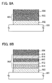
- FIGS. 8A and 8B each show a light-emitting element.
- FIGS. 9A to 9C show a passive-matrix light-emitting device.
- FIG. 10 shows a passive-matrix light-emitting device.
- FIGS. 11A and 11B show an active-matrix light-emitting device.
- FIGS. 12A to 12E each show an electronic appliance.
- FIGS. 13A to 13C show an electronic appliance.
- FIG. 14 is a graph showing regions in which conditions for first light and second light are satisfied.
- FIG. 15 shows a structure of a substrate which is used in a simulation.
- FIG. 16 is a graph showing a simulation result.
- Embodiment 1 a deposition method according to the present invention in which an evaporation donor substrate is used is described. Note that in Embodiment 1, a case is described where an evaporation material is patterned over the evaporation donor substrate and an EL layer of a light-emitting element is formed with use of the patterned evaporation material.
- a light absorption layer 102 is formed over a first substrate 101 , which is a supporting substrate, a reflective layer 104 having openings 103 is formed over the light absorption layer 102 , and a material layer 105 is formed over the light absorption layer 102 and the reflective layer 104 . Note that a part of the material layer 105 covers the openings 103 .
- the light absorption layer 102 , the reflective layer 104 having the openings 103 , and the material layer 105 are formed over the entire surface of the first substrate 101 .
- the first substrate 101 for example, a glass substrate, a quartz substrate, a plastic substrate containing an inorganic material, or a substrate formed using molybdenum and/or tungsten can be used.
- the light absorption layer 102 absorbs light which is used for irradiation in evaporation. Therefore, it is preferable that the light absorption layer 102 be formed using a material which has a low reflectance and high absorptance with respect to the irradiation light. Specifically, it is preferable that the light absorption layer 102 have a reflectance of 70% or lower with respect to the irradiation light.
- a material which can be used for the light absorption layer 102 for example, a metal nitride such as titanium nitride, tantalum nitride, molybdenum nitride, tungsten nitride, chromium nitride, and manganese nitride; molybdenum; titanium; tungsten; or carbon is preferably used.
- a metal nitride such as titanium nitride, tantalum nitride, molybdenum nitride, tungsten nitride, chromium nitride, and manganese nitride; molybdenum; titanium; tungsten; or carbon is preferably used.
- the light absorption layer 102 is not limited to a single layer and may include a plurality of layers.
- the material of the light absorption layer 102 needs to be selected as appropriate.
- the light absorption layer 102 can be formed by any of a variety of methods.
- the light absorption layer 102 can be formed by a sputtering method, an electron beam evaporation method, or a vacuum evaporation method.
- the light absorption layer 102 have a thickness with which the irradiation light is not transmitted (the thickness of 100 nm to 2 ⁇ m, inclusive, is preferable) although it depends on a material to be irradiated.
- the light absorption layer 102 can efficiently absorb the irradiation light to generate heat.
- the light absorption layer 102 having a thickness of 100 nm to 600 nm, inclusive allows highly accurate deposition onto the deposition target substrate.
- the light absorption layer 102 may partially transmit the irradiation light as long as the evaporation material contained in the material layer 105 can be heated up to the sublimation temperature. Note that in a case where the light absorption layer 102 partially transmits the irradiation light, it is preferable that a material which is not decomposed by light be used as the evaporation material contained in the material layer 105 .
- the reflective layer 104 When first light 107 enters the material layer 105 as shown in FIG. 1B , the reflective layer 104 has such a function that the first light 107 is selectively absorbed in a part of the light absorption layer 102 and reflected at the other part of the light absorption layer 102 . Therefore, the reflective layer 104 is preferably formed with a material having a high reflectance with respect to the first light 107 . Specifically, the reflective layer 104 preferably has a reflectance of 85% or more, more preferably, a reflectance of 90% or higher with respect to the irradiation light.
- examples of a material which can be used for the reflective layer 104 include aluminum, silver, gold, platinum, copper, an alloy containing aluminum (for example, an aluminum-titanium alloy, an aluminum-neodymium alloy, and an aluminum-titanium alloy), and an alloy containing silver (a silver-neodymium alloy).
- the reflective layer 104 can be formed by any of a variety of methods.
- the reflective layer 104 can be formed by a sputtering method, an electron beam evaporation method, or a vacuum evaporation method. It is preferable that the reflective layer 104 have a thickness of 100 nm or more although it depends on a material. With a thickness of 100 nm or more, the reflective layer 104 can suppress transmission of the irradiation light through the reflective layer 104 .
- a variety of methods can be used for formation of the openings 103 in this embodiment, and dry etching is preferably used. By dry etching, the openings 103 have sharper sidewalls, and thus a minute pattern can be deposited.
- the difference in reflectance with respect to the wavelength of the irradiation light is preferably 25% or higher, more preferably, 30% or higher.
- the material layer 105 includes the evaporation material, which is to be evaporated onto the deposition target substrate. Then, by irradiation of the evaporation donor substrate with light, the material layer 105 is heated and the evaporation material is sublimated and evaporated onto the deposition target substrate.
- any of a variety of materials can be used as the evaporation material included in the material layer 105 regardless of whether they are organic compounds or inorganic compounds, as long as the material can be evaporated.
- a material which can be evaporated to form an EL layer is used.
- an organic compound which forms an EL layer such as a light-emitting material or a carrier-transporting material, a carrier-injecting material, or an inorganic compound which is used for an electrode or the like of a light-emitting element, such as metal oxide, metal nitride, metal halide, or an elementary substance of metal can be used.
- an organic compound which forms an EL layer such as a light-emitting material or a carrier-transporting material, a carrier-injecting material, or an inorganic compound which is used for an electrode or the like of a light-emitting element, such as metal oxide, metal nitride, metal halide, or an elementary substance of metal can be used.
- the material layer 105 may include a plurality of materials.
- the material layer 105 may be a single layer or a stack of a plurality of layers. By stacking a plurality of layers each including an evaporation material, co-evaporation is possible. Note that in the case where the material layer 105 has a stacked-layer structure, it is preferable that the material layer 105 be formed over the first substrate so as to form an evaporation material having a low sublimation temperature (or a low evaporation temperature) closer to the first substrate. Such a structure allows the material layer 105 which has a stacked-layer structure to be efficiently evaporated.
- the material layer 105 is formed by any of a variety of methods.
- a wet method such as a spin coating method, a spray coating method, an ink-jet method, a dip coating method, a casting method, a die coating method, a roll coating method, a blade coating method, a bar coating method, a gravure coating method, or a printing method can be used.
- a dry method such as a vacuum evaporation method or a sputtering method can be used.
- a predetermined evaporation material may be dissolved or dispersed in a solvent, and a solution or a dispersion may be adjusted.
- a solvent There is no particular limitation on the solvent as long as it can dissolve or disperse the evaporation material and it does not react with the evaporation material.
- halogen-based solvents such as chloroform, tetra chloromethane, dichloromethane, 1,2-dichloroethane, and chlorobenzene
- ketone-based solvents such as acetone, methyl ethyl ketone, diethyl ketone, n-propyl methyl ketone, and cyclohexanone
- aromatic-based solvents such as benzene, toluene, and xylene
- ester-based solvents such as ethyl acetate, n-propyl acetate, n-butyl acetate, ethyl propionate, y-butyrolactone, and diethyl carbonate
- ether-based solvents such as tetrahydrofuran and dioxane
- amide-based solvents such as dimethylformamide and dimethylacetamide; dimethyl sulfoxide; hexane; water; and the like.
- a surface where the light absorption layer 102 , the reflective layer 104 , and the material layer 105 are formed over one surface of the first substrate 101 in this order is irradiated with the first light 107 .
- the light passes through the material layer 105 over the first substrate 101 , then, light which enters the reflective layer 104 is reflected while light which enters the openings 103 is absorbed by the light absorption layer 102 .
- the light absorption layer 102 absorbs light to generate heat and provides the heat to the evaporation material included in the material layer 105 to sublimate a part of the material layer 105 (see FIG. 1C ).
- the evaporation donor substrate in which a material layer 105 a is provided so as to overlap with the reflective layer 104 over the first substrate 101 can be formed (see FIG. 1D ).
- a laser is used as a light source of the first light 107 , which is used for irradiation.
- the first light 107 which is used for the irradiation, satisfies a general formula (1), preferably a general formula (2), which are given below, where light intensity is A 1 (W/cm 2 ) and irradiation time is B 1 (s).
- the general formula (1) given below corresponds to a region a ( 1401 ) in FIG. 14 . .
- the first light which is used for irradiation, passes through the material layer 105 and reaches the reflective layer 104 or the light absorption layer 102 . Therefore, in order to prevent deterioration of the material layer 105 , the first light is preferably has a wavelength of 450 nm or longer. For example, laser light with a wavelength of 488 nm, 514 nm, 527 nm, 532 nm, 561 nm, or 1024 nm can be used. In addition, the first light, which is used for irradiation, preferably has a wavelength with which the first light is absorbed as little as possible by the material layer 105 .
- a laser is used as a light source, conversion of the laser light into heat is sufficiently conducted in the light absorption layer 102 even if the irradiation time is short. Therefore, the precision of the shape of the material layer 105 a formed by the partial sublimation of the evaporation material can be improved.
- laser light emitted from one or more of the following can be used: a gas laser such as an Ar laser, a Kr laser, or an excimer laser; a solid-state laser medium of which is single-crystal YAG, YVO 4 , forsterite (Mg 2 SiO 4 ), YAlO 3 , or GdVO 4 , or polycrystalline (ceramic) YAG, Y 2 O 3 , YVO 4 , YAlO 3 , or GdVO 4 which is doped with one or more of Nd, Yb, Cr, Ti, Ho, Er, Tm, and Ta as a dopant; a glass laser; a ruby laser; an alexandrite laser; a Ti:sapphire laser; or a fiber laser.
- a gas laser such as an Ar laser, a Kr laser, or an excimer laser
- a second harmonic or a third harmonic emitted from the aforementioned solid-state laser can be used. Note that when a solid-state laser whose laser medium is solid is used, there are advantages in that a maintenance-free condition can be maintained for a long time and output power is relatively stable.
- a pulsed laser beam, a continuous-wave (CW) laser beam, or the like can be emitted from the aforementioned lasers.
- pulsed laser light for example, by using not only laser light having a repetition rate of several Hz to several hundreds of kHz but also laser light having a repetition rate of 1 MHz or greater can be used.
- a laser spot preferably has a linear shape or a rectangular shape.
- the material layer 105 is heated not with radiation heat from the irradiation light but with heat conducted by the light absorption layer 102 which absorbs the irradiation light. Therefore, heat is conducted in a lateral direction of the absorption layer 102 , from a part of the light absorption layer 102 which is irradiated with light to the other part of the light absorption layer 102 which is not irradiated with the light. Therefore, it is preferable to set light irradiation time of the material layer 105 be short so that an area of the material layer 105 which is heated is not enlarged. In particular, in the case of a pulsed laser, the length of the major axis of the laser spot can be increased to approximately 1 m, whereby processing time is shortened and productivity is improved.
- pattern formation of the material layer 105 is preferably performed under a reduced-pressure atmosphere by the light irradiation. Accordingly, it is preferable that a reaction chamber have a pressure of 5 ⁇ 10 ⁇ 3 Pa or less, more preferably, 10 ⁇ 6 Pa to 10 ⁇ 4 Pa, inclusive.
- the second substrate 201 is a deposition target substrate onto which a desired layer is to be deposited by evaporation treatment using the evaporation donor substrate. Note that since the case where an EL layer of a light-emitting element is formed using an evaporation donor substrate is described here, a first electrode 202 which is to be one of electrodes of the light-emitting element is formed over the second substrate 201 .
- the first substrate 101 and the second substrate 201 are arranged so as to face each other in proximity; specifically, they are arranged close to each other so that the distance d 2 between the surface of the material layer 105 a of the first substrate 101 and a surface of the second substrate 201 (in particular, a surface of the first electrode 202 ) becomes 0 ⁇ m to 10 ⁇ m, inclusive, preferably, 0 ⁇ m to 5 ⁇ m, inclusive, or more preferably, 0 ⁇ m to 3 ⁇ m, inclusive.
- the distance d 2 is defined as the distance between the outermost surface of the first substrate 101 and the outermost surface of the second substrate 201 . Therefore, when the first electrode 202 is formed over the second substrate 201 and an insulator 203 is formed over the second substrate 201 so as to cover an end portion of the first electrode 202 as shown in FIG. 3A , the distance d 2 is defined as the distance between the surface of the material layer 105 b over the first substrate 101 and a surface of the insulator 203 formed over the second substrate 201 .
- the distance d 2 is defined as the shortest distance between the surface of the material layer 105 b over the first substrate 101 and the outermost surface of the insulator 203 formed over the second substrate 201 .
- a rear surface of the first substrate 101 (the rear surface at which the light absorption layer 102 , the reflective layer 104 , and the material layer 105 a are not provided) is irradiated with second light 204 .
- heat generated in the light absorption layer 102 is conducted to the reflective layer 104 and the material layer 105 a which is overlapped with and adjusted to the reflective layer 104 is heated, whereby the evaporation material in the material layer 105 a is evaporated onto the first electrode 202 formed over the second substrate 201 .
- an EL layer 205 of a light-emitting element can be formed. Note that the same applies to a structure shown in FIGS. 3A to 3C .
- an EL layer 206 of a light-emitting element is formed over the first electrode 202 formed over the second substrate 201 .
- the second irradiation light 204 which is used for the irradiation, satisfies a general formula (3), preferably a general formula (4), which are given below, where light intensity is A 2 (W/cm 2 ) and irradiation time is B 2 (s). Note that the general formula (3) given below is satisfied in a region b ( 1402 ) in FIG. 14 . 1/ A 2 1.5 ⁇ B 2 ⁇ 10 6 /A 2 1.5 and B 2 ⁇ 10 ⁇ 4 (s) (3) 10/ A 2 1.5 ⁇ B 2 ⁇ 10 5 /A 2 1.5 and B 2 ⁇ 10 ⁇ 4 (s) (4)
- irradiation with the second light in the range of the general formula (3) allows the heat generated in the light absorption layer 102 to be conducted to the reflective layer 104 , whereby the material layer 105 a which is overlapped with and adjusted to the reflective layer 104 can be evaporated onto the second substrate.
- a lamp with which a large area can be irradiated at one time is preferably used as its light source.
- light irradiation time is preferably long.
- the whole first substrate 101 can be heated to a temperature of 500° C. or higher by irradiation for approximately 7 s, whereby the evaporation material in the material layer 105 a or 105 b can be sublimated.
- a discharge lamp such as a flash lamp (a xenon flash lamp, a krypton flash lamp, or the like), a xenon lamp, or a metal halide lamp, or an exothermic lamp, such as a halogen lamp or a tungsten lamp, can be used.
- a flash lamp enables irradiation on a large area for a short time (0.1 milliseconds to 10 milliseconds).
- the amount of light which enters the second substrate 201 can also be controlled by changing time interval of light emission.
- a flash lamp has a long lifetime and consumes less power on standby for light emission; accordingly, running cost can be reduced.
- evaporation by the light irradiation is preferably performed under a reduced-pressure atmosphere. Accordingly, it is preferable that a deposition chamber have a pressure of 5 ⁇ 10 ⁇ 3 Pa or less, more preferably, 10 ⁇ 6 Pa to 10 ⁇ 4 Pa, inclusive.
- the light absorption layer 102 absorbs light from a light source and provides heat to the material layer 105 a
- the evaporation material in the material layer 105 a may be sublimated not only by light irradiation but also by direct heating with use of a heat source, such as a heater.
- the distance d 2 between the first substrate 101 and the second substrate 201 may be set to be 0 ⁇ m. That is, the first substrate 101 and the second substrate 201 may be arranged so that the material layer 105 a of the first substrate 101 and the surface of the first electrode 202 formed over the second substrate 201 face each other and are in contact with each other. In this manner, reduction in the distance d 2 can prevent misplacement of a deposition region, and thus can prevent deformation of a deposition pattern over the deposition target surface. Accordingly, an EL layer 207 of a light-emitting element can be formed over the second substrate 201 with high accuracy. Note that in the case of FIG.
- an EL layer 208 of the light-emitting element can be formed with high accuracy so as to be in contact with the first electrode 202 over the second substrate 201 as shown in FIG. 3C .
- the second substrate 201 is provided below the first substrate 101 ; however, the present invention is not limited thereto.
- the second substrate 201 can be set over the first substrate 101 as appropriate.
- laser light is used as the first light 107 in the irradiation for the pattern formation of the material layer over the evaporation donor substrate, whereby efficient conversion of the laser light into heat in the light absorption layer can be realized with brief light irradiation. Therefore, the precision of the shape of the material layer 105 a formed by the partial sublimation of the evaporation material can be improved.
- the second light 204 whose light source is a lamp or the like in evaporating the patterned material layer onto the deposition target substrate, a large area can be irradiated at one time. Therefore, the light absorption layer 102 , which is formed on the entire surface of the first substrate 101 , can absorb light efficiently, which leads to improvement in deposition efficiency in evaporating the evaporation material onto the deposition target substrate.
- the precision of the shape of the layer evaporated onto the deposition target substrate can be improved because the material layer having a desired shape is formed over the evaporation donor substrate due to first light irradiation which partly sublimates the evaporation material, and then the material layer is evaporated onto the deposition target substrate.
- Simulation was performed to calculate change of temperatures of the substrate which was irradiated with the first light under the condition indicated by the X point in FIG. 14 .
- the X point indicates the condition that the irradiation time is 10 ⁇ s and the light intensity is 1.2 ⁇ 10 5 (W/cm 2 ).
- FIG. 15 shows a substrate which is used for the simulation.
- a substrate 1501 is a glass substrate having a thickness of 0.7 mm
- an absorption layer 1502 includes Ti and has a thickness of 150 nm
- a reflective layer 1503 includes Al and has a thickness of 600 nm and a width of 120 ⁇ m
- a material layer 1504 includes an evaporation material and has a thickness of 50 nm.
- a temperature of a surface of the material layer 1504 on each point which has a different distance from the center of the reflective layer 1503 was calculated by the simulation. Note that in FIG. 15 , the points A, B, C, and D have a distance of 200 ⁇ m, 60.1 ⁇ m, 60.0 ⁇ m, and 55.5 ⁇ m, respectively, from the center of the reflective layer 1503 .
- the point A and the point B of the material layer 1504 do not overlap with the reflective layer 1503 ; therefore, these regions of the material layer 1504 are heated (the region is referred to as a heated region).
- the point C and the point D of the material layer 1504 overlap or are in contact with the reflective layer 1503 ; therefore, these regions of the material layer 1504 is not heated (the region is referred to as a non-heated region).
- the absorption layer 1502 has an absorption rate of 50% and heating value was 6 ⁇ 10 4 (W/cm 2 ). In addition, the heating value was constant during the irradiation time of 10 ⁇ s.
- FIG. 16 shows the simulation result.
- the start time of the irradiation is denoted as 0 s.
- the maximum temperatures of the points A, B, C, and D were 1063° C., 212° C., 168° C., and 130° C., respectively. Therefore, the difference between the maximum temperatures of the point B and the point C which indicates a boundary between the heated region and the non-heated region in the material layer 1504 was 44° C.
- Embodiment 2 an apparatus is described which is used when an evaporation donor substrate is irradiated with laser light as the first light in a deposition method using the evaporation donor substrate described in Embodiment 1.
- FIG. 4 is a perspective view illustrating an example of an apparatus using laser light.
- Laser light is outputted from a laser device 403 (a YAG laser device, an excimer laser device, or the like) and transmitted through a first optical system 404 for changing a laser light shape into a rectangular shape, a second optical system 405 for shaping the laser light, and a third optical system 406 for collimating the laser light.
- a laser device 403 a YAG laser device, an excimer laser device, or the like
- a first optical system 404 for changing a laser light shape into a rectangular shape
- a second optical system 405 for shaping the laser light
- a third optical system 406 for collimating the laser light.
- an optical path is bent to a direction perpendicular to an evaporation donor substrate which is a first substrate 401 over a first substrate stage 409 by using a reflecting mirror 407 .
- the laser light enters the evaporation donor substrate 401 .
- the structure of the evaporation donor substrate described in Embodiment 2 is similar to that described in Embodiment 1. That is, the first substrate 401 has the structure in which a reflective layer, a light absorption layer, and a material layer are formed. Note that the reflective layer is formed in a region 413 illustrated with a dotted line in FIG. 4 .
- the shape of a laser spot on the first substrate 401 preferably has a rectangular shape or a linear shape. Furthermore, in the case of using a large-area substrate, a laser spot preferably has a longer side of 20 cm to 100 cm in order to shorten processing time. Moreover, a plurality of laser devices and optical systems shown in FIG. 4 may be provided so that a substrate with a large area can be processed in a short time. Specifically, laser beams may be emitted from the plurality of laser devices to process divided areas of one substrate.
- FIG. 4 shows an example, and there is no particular limitation on a positional relationship between optical systems or an electro-optical element placed in the optical path of the laser light.
- the reflective mirror 407 is not always needed if the laser device 403 is placed above the first substrate 401 so that laser light is emitted from the laser device 403 in a direction perpendicular to a principle plane of the first substrate 401 .
- an optical system may be a condenser lens, a beam expander, a homogenizer, a polarizer, or the like, and these may be combined. Further, an optical system may be combined with a slit.
- a control device 416 controls a moving means (not illustrated) for moving the first substrate stage 409 which holds the first substrate 401 , which is an evaporation donor substrate, in the XY direction, whereby scanning is performed.
- the control device 416 is preferably interlocked so as to also control the laser device 403 .
- the control device 416 is preferably interlocked with a position alignment unit 408 which has an imaging device for detecting a position marker.
- At least the first substrate 401 is placed in a vacuum chamber.
- all of the components shown in FIG. 4 may be placed in the vacuum chamber.
- the material layer over the evaporation donor substrate can be patterned. Further, in this pattern formation, the evaporation material evaporated can be collected to be reused. In that case, manufacturing cost can be reduced.
- Embodiment 2 can be combined with a structure which is described in Embodiment 1 as appropriate.
- Embodiment 3 an apparatus is described which is used in the case where an evaporation donor substrate having a patterned material layer is irradiated with lamp light used as a second light in a deposition method using the evaporation donor substrate described in Embodiment 1.
- a deposition chamber 501 which is a vacuum chamber is interlocked with another process chamber with a gate valve 502 and is provided with an exhaust unit 503 .
- the deposition chamber 501 is at least provided with a substrate stage 504 for holding a first substrate 511 (including a material layer 513 ), which is an evaporation donor substrate, a supporting unit 505 to support a substrate for holding a second substrate 512 which is a deposition target substrate, and a light source 510 .
- a material layer of the first substrate 511 held on the substrate stage 504 is patterned by treatment described in Embodiment 1 or Embodiment 2 which is performed in another processing chamber. That is, after the material layer of the first substrate 511 is patterned in another process chamber, the resulting substrate is transferred to the deposition chamber 501 and set on the substrate stage 504 . Further, the second substrate 512 , which is a deposition target substrate, is fixed to the supporting unit 505 to support a substrate so that a surface provided with the material layer 513 of the first substrate 511 faces a deposition target surface of the second substrate 512 .
- the first substrate 511 and the second substrate 512 are brought closer to each other so that the distance between the first substrate 511 and the second substrate 512 becomes the distance d.
- the distance d is defined as the distance between the surface of the material layer 513 formed over the first substrate 511 and the surface of the second substrate 512 .
- some layer for example, a conductive layer which functions as an electrode or an insulator which functions as a partition
- the distance d is defined as the distance between the surface of the material layer 513 over the first substrate 511 and a surface of the layer formed on the second substrate 512 .
- the distance d is defined as the shortest distance between the surface of the material layer 513 over the first substrate 511 and the outermost surface of the second substrate 512 or the layer formed on the second substrate 512 .
- the distance d is 0 ⁇ m to 10 ⁇ m, inclusive, preferably, 0 mm to 5 ⁇ m, inclusive, more preferably, 0 ⁇ m to 3 ⁇ m, inclusive.
- the distance d is 2 ⁇ m.
- the second substrate 512 is hard like a quartz substrate and formed of a material which is unlikely to be deformed (warped, bent, or the like)
- the distance d can be reduced to 0 ⁇ m as the minimum distance.
- FIGS. 5A and 5B show cross sections in a step in which the supporting unit 505 to support a substrate is moved so that the first substrate 511 and the second substrate 512 are brought closer to each other to have the distance d therebetween.
- the substrate stage 504 and the supporting unit 505 to support a substrate are provided with a moving means (not illustrated) which moves the substrate stage 504 and the supporting unit 505 to support a substrate not only in a vertical direction but also in the XY direction, and precise arrangement is performed by controlling the moving means by a control device 506 .
- the control device 506 is preferably interlocked with a position alignment unit 507 which has an imaging device for detecting a position marker over the substrate (in this case, the second substrate 512 ).
- a sensor for measuring the temperature or humidity inside the deposition chamber 501 may be provided.
- the material layer 513 which is patterned over the first substrate 511 is heated in a short time, and an evaporation material included in the material layer 513 is sublimated; thus, the evaporation material is deposited onto the deposition target surface (i.e., a lower surface) of the second substrate 512 which is placed so as to face the first substrate 511 .
- the deposition target surface i.e., a lower surface
- a film with a uniform and desired thickness can be deposited onto the second substrate 512 without providing a thickness monitor.
- the deposition target substrate is fixed during deposition in the deposition apparatus shown in FIGS. 5A and 5B ; thus, this deposition apparatus is suitable for deposition onto a large-area glass substrate which is easily broken.
- the evaporation donor substrate is also fixed during deposition.
- the light source 510 be faced with a large area of the first substrate 511 , which is the evaporation donor substrate, for uniform heating.
- an openable and closable shutter used for heat insulation on standby may be provided between the light source 510 and the first substrate 511 .
- a discharge lamp such as a flash lamp (a xenon flash lamp, a krypton flash lamp, or the like), a xenon lamp, or a metal halide lamp, or an exothermic lamp, such as a halogen lamp or a tungsten lamp, can be used.
- a flash lamp is capable of repeatedly emitting very high-intensity light for a short time (0.1 msec to 10 msec) over a large area; thus, heating can be performed uniformly and efficiently regardless of the area of the first substrate.
- heating of the first substrate 511 can be controlled by changing time interval of light emission.
- a flash lamp has a long lifetime and consumes less power on standby for light emission; accordingly, running cost can be reduced.
- a flash lamp facilitates rapid heating, a vertical movement unit, a shutter, and the like in the case of using a heater can be simplified. Thus, further reduction in size of the deposition apparatus can be achieved.
- FIGS. 5A and 5B show an example in which the light source 510 is placed in the deposition chamber 501
- a part of an inner wall of the deposition chamber may be made of a light-transmitting member and the light source 510 may be placed outside the deposition chamber.
- the light source 510 is placed outside the deposition chamber 501 , maintenance such as replacement of light bulbs of the light source 510 can be facilitated.
- a unit for controlling the temperature of the second substrate 512 may be provided.
- a cooling unit is provided as a unit for controlling the temperature
- the supporting unit 505 to support a substrate can be used as cold plates. Provision of a cooling unit in this manner is useful in the case where different kinds of material layers are stacked.
- the supporting unit 505 to support a substrate may be provided with a heating means such as a heater 520 .
- FIGS. 5A and 5B show the example of the deposition apparatus employing a face-down system in which the deposition target surface of the second substrate 512 faces downward, a deposition apparatus employing a face-up system in which the deposition surface of the second substrate 512 faces upward can also be used. Further, although FIGS. 5A and 5B show the example of the deposition apparatus employing a system in which the substrate are horizontally placed, a deposition apparatus employing a system in which the substrates are vertically placed can also be used.
- the material layer over the evaporation donor substrate can be evaporated onto the deposition target substrate.
- the material layer over the evaporation donor substrate is patterned in advance; therefore, the evaporation material can be evaporated onto the deposition target substrate with high accuracy.
- a film can be deposited onto a large area at one time, whereby tact time can be shortened and manufacturing cost of a light-emitting device can be reduced.
- Embodiment 3 can be combined with a structure which is described in Embodiment 1 or 2 as appropriate.
- Embodiment 4 a method for manufacturing a light-emitting device which is capable of full-color display is described.
- EL layers of light-emitting elements are formed using a plurality of evaporation donor substrates which are described in Embodiment 1.
- Embodiment 1 through one deposition process, EL layers containing the same kind of material are formed over the second substrate, which is a deposition target substrate. Described in Embodiment 4 is the case where EL layers of three different emission colors are formed over different places of the second substrate.
- first substrates each of which is the evaporation donor substrate illustrated in FIG. 1D in Embodiment 1 are prepared.
- a material layer including an evaporation material for forming an EL layer of a different emission color is formed over each substrate.
- a first substrate (B) having a material layer (B) for forming an EL layer exhibiting blue light emission an EL layer (B)
- one second substrate which is the deposition target substrate illustrated in FIG. 2A in Embodiment 1 is prepared. Note that a plurality of the first electrodes 202 are formed over the second substrate.
- the second substrate and the first substrate (R) are superimposed on each other and positioned for a first deposition process as in FIG. 2A .
- the second substrate is preferably provided with a position marker.
- the first substrate (R) is preferably provided with a position marker. Note that because the first substrate (R) is provided with a light absorption layer, a portion of the light absorption layer near the position marker is preferably removed in advance. Further, the material layer (R) over the first substrate (R) is patterned to be left only at positions which overlap with a reflective layer (R) 601 .
- a rear surface of the first substrate (R) (the surface on which the light absorption layer 102 , the reflective layer 104 , and the material layer 105 a , which are shown in FIG. 2A , are not formed) is irradiated with light.
- the light absorption layer 102 absorbs the irradiation light and provides heat which is conducted over a surface of the light absorption layer 102 for the material layer (R), whereby the evaporation material included in the material layer (R) is sublimated.
- an EL layer (R) 611 is formed over some of the first electrodes over the second substrate 201 .
- the first substrate (R) is moved away from the second substrate 201 .
- the second substrate 201 and the first substrate (G) are superimposed on each other and positioned for a second deposition process.
- the material layer (G) over the first substrate (G) is formed at a position which is shifted by one pixel from the material layer (R) formed over the first substrate (R), which is used in the first deposition.
- a rear surface of the first substrate (G) (the surface on which the light absorption layer 102 , the reflective layer 104 , and the material layer 105 a , which are shown in FIG. 2A , are not formed) is irradiated with light.
- the light absorption layer 102 absorbs the irradiation light and provides heat which is conducted over a surface of the absorption layer 102 for the material layer (G), whereby the evaporation material included in the material layer (G) is sublimated.
- an EL layer (G) 611 is formed over first electrodes which are over the second substrate 201 and which are next to the first electrodes over which the EL layer (R) is formed in the first deposition.
- the first substrate (G) is moved away from the second substrate 201 .
- the second substrate 201 and the first substrate (B) are superimposed on each other and positioned for a third deposition process.
- the material layer (B) over the first substrate (B) is formed at a position which is shifted by two pixels from the material layer (R) formed over the first substrate (R), which is used in the first deposition.
- a rear surface of the first substrate (B) (the surface on which the light absorption layer 102 , the reflective layer 104 , and the material layer 105 a , which are shown in FIG. 2A , are not formed) is irradiated with light.
- a state before the third deposition corresponds to a top view of FIG. 6A .
- the material layer (B) is formed at a position which overlaps with a reflective layer (B) 604 , and the light absorption layer 102 absorbs the irradiation light and provides heat which is conducted over a surface of the light absorption layer 102 for the material layer (B), whereby the evaporation material included in the material layer (B) is sublimated.
- an EL layer (B) 613 is formed over first electrodes which are over the second substrate 201 and which are next to the first electrodes over which the EL layer (G) is formed in the second deposition. After the third deposition is completed, the first substrate (B) is moved away from the second substrate 201 .
- the EL layer (R) 611 , the EL layer (G) 612 , and the EL layer (B) 613 can be formed at regular intervals over one second substrate. Then, a second electrode is formed over these films. Thus, light-emitting elements can be formed.
- FIGS. 6A and 6B show an example in which the reflective layers (the reflective layer (R) 601 , a reflective layer (G) 603 , and the reflective layer (B) 604 ) formed over the first substrates, which are evaporation donor substrates, have a rectangular shape
- an embodiment of the present invention is not particularly limited to this example.
- These reflective layers may be successively formed (in a so-called line shape) in the case where neighboring light-emitting regions emit light of the same color. Note that in the case where the reflective layers are formed in a line shape, deposition is performed also between light-emitting regions of the same color; therefore, an insulator or the like is preferably formed between the first electrodes which form the light-emitting regions.
- each pixel may be a polygon such as a hexagon as shown in FIG. 7A
- a full-color light-emitting device may be realized by arrangement of an EL layer (R) 711 , an EL layer (G) 712 , and an EL layer (B) 713 .
- deposition may be performed using the first substrate in FIG. 7B which is provided with the material layer (R) which is patterned to be left at a position overlapping with a polygonal reflective layer 701 .
- a minute pattern can be formed with high accuracy by the deposition method using the evaporation donor substrate of the present invention. Accordingly, a high-definition light-emitting device can be obtained, and further, the characteristics of the light-emitting device can be improved. In addition, evaporation material which becomes unnecessary after patterning the material layer can be collected and reused; therefore, manufacturing cost of the light-emitting device can be reduced.
- Embodiment 4 can be combined with a structure which is described in Embodiments 1 to 3 as appropriate.
- FIGS. 8A and 8B can be manufactured.
- a first electrode 802 , an EL layer 803 which includes only a light-emitting layer 813 , and a second electrode 804 are stacked in that order over a substrate 801 .
- One of the first electrode 802 and the second electrode 804 functions as an anode, and the other functions as a cathode. Holes injected from the anode and electrons injected from the cathode are recombined in the EL layer 803 , whereby light can be emitted from the EL layer 803 .
- the first electrode 802 functions as the anode and the second electrode 804 functions as the cathode.
- the EL layer 803 in FIG. 8A has a stacked structure including a plurality of layers. Specifically, a hole-injecting layer 811 , a hole-transporting layer 812 , the light-emitting layer 813 , an electron-transporting layer 814 , and an electron-injecting layer 815 are provided in that order over the first electrode 802 .
- the EL layer 803 functions as a light emitting layer as long as it includes at least the light-emitting layer 813 as in FIG. 8A ; therefore, all of the above layers are not always necessary and may be selected as appropriate to be provided as needed.
- a substrate having an insulating surface or an insulating substrate is employed as the substrate 801 in FIGS. 8A and 8B .
- the substrate include various types of glass substrates that are used in the electronics industry, such as an aluminosilicate glass substrate, an aluminoborosilicate glass substrate, or a barium borosilicate glass substrate; a quartz substrate; a ceramic substrate; and a sapphire substrate.
- any of various types of metals, alloys, electrically conductive compounds, mixtures thereof, and the like can be used. Specific examples are given below: indium tin oxide (ITO), indium tin oxide containing silicon or silicon oxide, indium zinc oxide (IZO), and indium oxide containing tungsten oxide and zinc oxide. Further, gold (Au), platinum (Pt), nickel (Ni), tungsten (W), chromium (Cr), molybdenum (Mo), iron (Fe), cobalt (Co), copper (Cu), palladium (Pd), nitride of a metal material (e.g., titanium nitride), or the like can be used.
- ITO indium tin oxide
- IZO indium zinc oxide
- gold (Au) platinum (Pt), nickel (Ni), tungsten (W), chromium (Cr), molybdenum (Mo), iron (Fe), cobalt (Co), copper (Cu), palladium (Pd), n
- a film of any of those materials is generally formed by a sputtering method.
- a film of indium zinc oxide can be formed by a sputtering method using a target in which zinc oxide is added to indium oxide at 1 wt % to 20 wt %.
- a film of indium oxide containing tungsten oxide and zinc oxide can be formed by a sputtering method using a target in which tungsten oxide and zinc oxide are added to indium oxide at 0.5 wt % to 5 wt % and 0.1 wt % to 1 wt %, respectively.
- a film of any of those materials may be formed by an inkjet method, a spin coating method, or the like by application of a sol-gel process or the like.
- any of the following materials having a low work function value can be used: elements which belong to Group 1 and Group 2 of the periodic table, that is, alkali metals such as lithium (Li) and cesium (Cs) and alkaline-earth metals such as magnesium (Mg), calcium (Ca), and strontium (Sr), and alloys thereof (an alloy of aluminum, magnesium, and silver, and an alloy of aluminum and lithium); rare earth metals such as europium (Eu) and ytterbium (Yb), and alloys thereof; and the like.
- alkali metals such as lithium (Li) and cesium (Cs)
- alkaline-earth metals such as magnesium (Mg), calcium (Ca), and strontium (Sr), and alloys thereof (an alloy of aluminum, magnesium, and silver, and an alloy of aluminum and lithium
- rare earth metals such as europium (Eu) and ytterbium (Yb), and alloys thereof; and the like.
- a film of an alkali metal, an alkaline earth metal, and an alloy thereof can be formed by a vacuum evaporation method.
- a film of an alloy containing an alkali metal or an alkaline earth metal can be formed by a sputtering method.
- a film of a silver paste or the like can be formed by an ink-jet method or the like.
- the first electrode 802 and the second electrode 804 are not limited to a single-layer film and can be formed as a stacked-layer film.
- one or both of the first electrode 802 and the second electrode 804 are formed so as to transmit light.
- one or both of the first electrode 802 and the second electrode 804 are formed using a conductive material having a light-transmitting property, such as indium tin oxide, or formed using silver, aluminum, or the like with a thickness of several nanometers to several tens of nanometers.
- first electrode 802 and the second electrode 804 can have a stacked-layer structure including a thin film of a metal such as silver, aluminum, or the like with a reduced thickness and a thin film of a conductive material having a light-transmitting property, such as ITO.
- a metal such as silver, aluminum, or the like with a reduced thickness
- a thin film of a conductive material having a light-transmitting property such as ITO.
- the EL layer 803 (the hole-injecting layer 811 , the hole-transporting layer 812 , the light-emitting layer 813 , the electron-transporting layer 814 , or the electron-injecting layer 815 ) of the light-emitting element of this embodiment can be formed by application of a deposition method which is described in Embodiments 1 to 4.
- a material layer of the evaporation donor substrate described in Embodiment 1 is formed using a material which forms the EL layer 803 and the EL layer 803 is formed over the first electrode 802 over the substrate 801 using the evaporation donor substrate. Then, the second electrode 804 is formed over the EL layer 803 , whereby the light-emitting element in FIG. 8A can be obtained.
- any of a variety of materials can be used for the light-emitting layer 813 .
- a fluorescent compound which exhibits fluorescence or a phosphorescent compound which exhibits phosphorescence can be used.
- Examples of a phosphorescent compound which is used for the light-emitting layer 813 are given below.
- a material for blue light emission bis[2-(4′,6′-difluorophenyl)pyridinato-N,C 2 ′]iridium(III)tetrakis(1-pyrazolyl)borate (abbr.: FIr6), bis[2-(4′,6′-difluorophenyl)pyridinato-N,C 2 ′]iridium(III)picolinate (abbr.: FIrpic), bis[2-(3′,5′bistrifluoromethylphenyl)pyridinato-N,C 2 ′]iridium(III)picolinate (abbr.: Ir(CF 3 ppy) 2 (pic)), bis[2-(4′,6′-difluorophenyl)pyridinato-N,C 2 ′]iridium(III)acetylacetonate (
- tris(2-phenylpyridinato-N,C 2 ′)iridium(III) (abbr.: Ir(ppy) 3 ), bis[2-phenylpyridinato-N,C 2 ′]iridium(III)acetylacetonate (abbr.: Ir(ppy) 2 (acac)), bis(1,2-diphenyl-1H-benzimidazolato)iridium(III)acetylacetonate (abbr.: Ir(pbi) 2 (acac)), bis(benzo[h]quinolinato)iridium(III)acetylacetonate (abbr.: Ir(bzq) 2 (acac)), or the like can be given.
- bis(2,4-diphenyl-1,3-oxazolato-N,C 2 ′)iridium(III)acetylacetonate (abbr.: Ir(dpo) 2 (acac)), bis[2-(4′-perfluorophenylphenyl)pyridinato]iridium(III)acetylacetonate (abbr.: Ir(p-PF-ph) 2 (acac)), bis(2-phenylbenzothiazolato-N,C 2 ′)iridium(III)acetylacetonate (abbr.: Ir(bt) 2 (acac)), or the like can be given.
- Ir(dpo) 2 (acac) bis[2-(4′-perfluorophenylphenyl)pyridinato]iridium(III)acetylacetonate
- Ir(p-PF-ph) 2 (acac) bis(2-phenylbenz
- tris(2-phenylquinolinato-N,C 2 ′)iridium(III) (abbr.: Ir(pq) 3 ), bis(2-phenylquinolinato-N,C 2 ′)iridium(III)acetylacetonate (abbr.: Ir(pq) 2 (acac)), or the like can be given.
- an organometallic complex such as bis[2-(2′-benzo[4,5-a]thienyl)pyridinato-N,C 3 ′]iridium(III)acetylacetonate (abbr.: Ir(btp) 2 (acac)), bis(1-phenylisoquinolinato-N,C 2 ′)iridium(III)acetylacetonate (abbr.: Ir(piq) 2 (acac)), (acetylacetonato)bis[2,3-bis(4-fluorophenyl)quinoxalinato]iridium(III) (abbr.: Ir(Fdpq) 2 (acac)), 2,3,7,8,12,13,17,18-octaethyl-21H,23H -porphyrinatoplatinum(III) (abbr.: PtOEP), or the like can be given.
- Ir(btp) 2 (acac)
- a rare earth metal complex such as tris(acetylacetonato)(monophenanthroline)terbium(III) (abbr.: Tb(acac) 3 (Phen)), tris(1,3-diphenyl-1,3-propanedionato)(monophenanthroline)europium(III) (abbr.: Eu(DBM) 3 (Phen)), or tris[1-(2-thenoyl)-3,3,3-trifluoroacetonato](monophenanthroline)europium(III) (abbr.: Eu(TTA) 3 (Phen)) exhibits light emission from a rare earth metal ion (electron transition between different multiplicities); therefore, such a rare earth metal complex can be used as a phosphorescent compound.
- Examples of a fluorescent compound which is used for the light-emitting layer 813 are given below.
- a material for blue light emission N,N′-bis[4-(9H-carbazol-9-yl)phenyl]-N,N′-diphenylstilbene-4,4′-diamine (abbr.: YGA2S), 4-(9H-carbazol-9-yl)-4′-(10-phenyl-9-anthryl)triphenylamine (abbr.: YGAPA), or the like can be given.
- N-(9,10-diphenyl-2-anthryl)-N,9-diphenyl-9H-carbazol-3-amine (abbreviation, 2PCAPA), N-[9,10-bis(1,1′-biphenyl-2-yl)-2-anthryl]-N,9-diphenyl-9H-carbazol-3-amine (abbr.: 2PCABPhA), N-(9,10-diphenyl-2-anthryl)-N,N′,N′-triphenyl-1,4-phenylenediamine (abbr.: 2DPAPA), N-[9,10-bis(1,1′-biphenyl-2-yl)-2-anthryl]-N,N′,N′-triphenyl-1,4-phenylenediamine (abbr.: 2DPABPhA) 9,10-bis(1,1′-biphenyl-2-yl)-N-[4-(9H-
- rubrene 5,12-bis(1,1′-biphenyl-4-yl)-6,11-diphenyltetracene (abbr.: BPT), or the like can be given.
- BPT 5,12-bis(1,1′-biphenyl-4-yl)-6,11-diphenyltetracene
- red light emission N,N,N′,N′-tetrakis(4-methylphenyl)tetracene-5,11-diamine (abbr.: p-mPhTD), 7,13-diphenyl-N,N,N′,N′-tetrakis(4-methylphenyl)acenaphtho[1,2-a]fluoranthene-3,10-diamine (abbr.: p-mPhAFD), or the like can be given.
- the light-emitting layer 813 may have a structure in which a substance having a high light-emitting property (a dopant material) is dispersed in another substance (a host material), whereby crystallization of the light-emitting layer can be suppressed.
- concentration quenching of the light-emitting layer 813 which results from high concentration of the substance having a high light-emitting property can be suppressed.
- the substance having a high light-emitting property is a fluorescent compound
- a substance having higher singlet excitation energy the energy difference between a ground state and a singlet excited state
- the substance having a high light-emitting property is a phosphorescent compound
- a substance having higher triplet excitation energy the energy difference between a ground state and a triplet excited state
- Examples of host materials used for the light-emitting layer 813 are given below: 4,4′-bis[N-(1-naphthyl)-N-phenylamino]biphenyl (abbr.: NPB), tris(8-quinolinolato)aluminum(III) (abbr.: Alq), 4,4′-bis[N-(9,9-dimethylfluoren-2-yl)-N-phenylamino]biphenyl (abbr.: DFLDPBi), bis(2-methyl-8-quinolinolato)(4-phenylphenolato)aluminum(III) (abbr.: BAlq), 4,4′-di(9-carbazolyl)biphenyl (abbr.: CBP), 2-tert-butyl-9,10-di(2-naphthyl)anthracene (abbr.: t-BuDNA), and 9-[4-(9-carbazo
- any of the above-mentioned phosphorescent compounds and fluorescent compounds can be used.
- the light-emitting layer 813 has a structure in which a substance having a high light-emitting property (a dopant material) is dispersed in another substance (a host material), a mixed layer of a host material and a guest material is formed as the material layer over the evaporation donor substrate.
- the material layer over the evaporation donor substrate may have a structure in which a layer containing a host material and a layer containing a dopant material are stacked.
- the light-emitting layer 813 contains a substance in which a light-emitting material is dispersed (a host material) and a substance having a high light-emitting property (a dopant material), and has a structure in which the substance having a high light-emitting property (the dopant material) is dispersed in the substance in which a light-emitting material is dispersed (the host material).
- a host material a substance having a high light-emitting property
- the host material the substance having a high light-emitting property
- two or more kinds of host materials and a dopant material may be used, or two or more kinds of dopant materials and a host material may be used.
- two or more kinds of host materials and two or more kinds of dopant materials may be used.
- an evaporation donor substrate described in Embodiment 1 which has a material layer for forming a layer (the hole-injecting layer 811 , the hole-transporting layer 812 , the electron-transporting layer 814 , or the electron-injecting layer 815 ) included in the EL layer 803 is prepared for each layer, and deposition of each layer is performed using a different evaporation donor substrate by the method described in Embodiment 1, whereby the EL layer 803 is formed over the first electrode 802 over the substrate 801 . Then, the second electrode 804 is formed over the EL layer 803 , whereby the light-emitting element in FIG. 8B can be obtained. Note that although all the layers in the EL layer 803 can be formed by the method described in Embodiment 1 in this case, only some of the layers in the EL layer 803 may be formed by the method described in Embodiment 1.
- the hole-injecting layer 811 can be formed using molybdenum oxide, vanadium oxide, ruthenium oxide, tungsten oxide, manganese oxide, or the like.
- the hole-injecting layer 811 can be formed using a phthalocyanine-based compound such as phthalocyanine (abbr.: H 2 Pc) or copper phthalocyanine (abbr.: CuPc), a high molecular compound such as poly(3,4-ethylenedioxythiophene)/poly(styrenesulfonate) (PEDOT/PSS), or the like.
- the hole-injecting layer 811 a layer which contains a substance having a high hole-transporting property and a substance having an electron-accepting property can be used.
- the layer which contains a substance having a high hole-transporting property and a substance having an electron-accepting property has a high carrier density and an excellent hole-injecting property.
- a material of the electrode that functions as an anode can be selected from any of a variety of metals, alloys, electrically conductive compounds, mixtures thereof, and the like can be used for the electrode regardless of the value of the work function.
- the layer which contains a substance having a high hole-transporting property and a substance having an electron-accepting property can be formed using, for example, an evaporation donor substrate having a material layer which is a stack of a layer containing a substance having a high hole-transporting property and a layer containing a substance having an electron-accepting property.
- Examples of the substance having an electron-accepting property which is used for the hole-injecting layer 811 are given below: 7,7,8,8-tetracyano-2,3,5,6-tetrafluoroquinodimethane (abbr.: F4-TCNQ), chloranil, and the like.
- Other examples include a transition metal oxide.
- Still other examples include oxide of metals belonging to Group 4 to Group 8 of the periodic table.
- vanadium oxide, niobium oxide, tantalum oxide, chromium oxide, molybdenum oxide, tungsten oxide, manganese oxide, and rhenium oxide are preferable because of their high electron-accepting properties.
- molybdenum oxide is especially preferable because molybdenum oxide is stable also in the atmosphere and has a low hygroscopic property, and therefore, can be easily handled.
- the substance having a high hole-transporting property which is used for the hole-injecting layer 811 any of various compounds such as an aromatic amine compound, a carbazole derivative, an aromatic hydrocarbon, and a high molecular compound (such as an oligomer, a dendrimer, and a polymer) can be used.
- the substance having a high hole-transporting property used for the hole-injecting layer be a substance having a hole mobility of 10 ⁇ 6 cm 2 /Vs or higher.
- any other material whose hole-transporting property is higher than its electron-transporting property may be used. Specific examples of the substance having a high hole-transporting property which can be used for the hole-injecting layer 811 are given below.
- Examples of an aromatic amine compound which can be used for the hole-injecting layer 811 are given below: 4,4′-bis[N-(1-naphthyl)-N-phenylamino]biphenyl (abbr.: NPB), N,N′-bis(3-methylphenyl)-N,N′-diphenyl-[1,1′-biphenyl]-4,4′-diamine (abbr.: TPD), 4,4′,4′′-tris(N,N-diphenylamino)triphenylamine (abbr.: DATA), 4,4′,4′′-tris[N-(3-methylphenyl)-N-phenylamino]triphenylamine (abbr.: MTDATA), and 4,4′-bis[N-(spiro-9,9′-bifluoren-2-yl)-N-phenylamino]biphenyl (abbr.: BSPB).
- NPB N,N′
- N,N-bis(4-methylphenyl)(p-tolyl)-N,N′-diphenyl-p-phenylenediamine abbreviations: DTDPPA
- DTDPPA 4,4′-bis[N-(4-diphenylaminophenyl)-N-phenylamino]biphenyl
- DPAB 4,4′-bis(N-4-[N′-(3-methylphenyl)-N′-phenylamino]phenyl-N -phenylamino)biphenyl
- DNTPD 1,3,5-tris[N-(4-diphenylaminophenyl)-N-phenylamino]benzene
- DPA3B 1,3,5-tris[N-(4-diphenylaminophenyl)-N-phenylamino]benzene
- carbazole derivative which can be used for the hole-injecting layer 811 are given below: 3-[N-(9-phenylcarbazol-3-yl)-N-phenylamino]-9-phenylcarbazole (abbr.: PCzPCA1), 3,6-bis[N-(9-phenylcarbazol-3-yl)-N-phenylamino]-9-phenylcarbazole (abbr.: PCzPCA2), and 3-[N-(1-naphthyl)-N-(9-phenylcarbazol-3-yl)amino]-9-phenylcarbazole (abbr.: PCzPCN1).
- carbazole derivative which can be used for the hole-injecting layer 811 are given below: 4,4′-di(N-carbazolyl)biphenyl (abbr.: CBP), 1,3,5-tris[4-(N-carbazolyl)phenyl]benzene (abbr.: TCPB), 9-[4-(10-phenyl-9-anthryl)phenyl]-9H-carbazole (abbr.: CzPA), and 1,4-bis-[4-(N-carbazolyl)phenyl]-2,3,5,6-tetraphenylbenzene.
- CBP 4,4′-di(N-carbazolyl)biphenyl
- TCPB 1,3,5-tris[4-(N-carbazolyl)phenyl]benzene
- CzPA 9-[4-(10-phenyl-9-anthryl)phenyl]-9H-carbazole
- Examples of an aromatic hydrocarbon which can be used for the hole-injecting layer 811 are given below: 2-tert-butyl-9,10-di(2-naphthyl)anthracene (abbr.: t-BuDNA), 2-tert-butyl-9,10-di(1-naphthyl)anthracene, 9,10-bis(3,5-diphenylphenyl)anthracene (abbr.: DPPA), 2-tert-butyl-9,10-bis(4-phenylphenyl)anthracene (abbr.: t -BuDBA), 9,10-di(2-naphthyl)anthracene (abbr.: DNA), 9,10-diphenylanthracene (abbr.: DPAnth), 2-tert-butylanthracene (abbr.: t-BuAnth), 9,10-bis(4-methyl-1-naphthyl)an
- aromatic hydrocarbons listed here it is preferable that an aromatic hydrocarbon having a hole mobility of 1 ⁇ 10 ⁇ 6 cm 2 /Vs or higher and having 14 to 42 carbon atoms be used.
- an aromatic hydrocarbon which can be used for the hole-injecting layer 811 may have a vinyl skeleton.
- Examples of an aromatic hydrocarbon having a vinyl group are given below: 4,4′-bis(2,2-diphenylvinyl)biphenyl (abbr.: DPVBi), and 9,10-bis[4-(2,2-diphenylvinyl)phenyl]anthracene (abbr.: DPVPA).
- the hole-injecting layer 811 can be formed by using an evaporation donor substrate having a material layer which is a stack of a layer containing a substance having a high hole-transporting property and a layer containing a substance having an electron-accepting property.
- metal oxide is used as the substance having an electron-accepting property, it is preferable that a layer which contains the metal oxide be formed after the layer which contains a substance having a high hole-transporting property is formed over the first substrate 801 . This is because, in many cases, metal oxide has a higher decomposition temperature or evaporation temperature than a substance having a high hole-transporting property.
- the evaporation source with such a structure makes it possible to efficiently sublimate a substance having a high hole-transporting property and metal oxide.
- local non-uniformity of concentration of the metal oxide in a deposited film formed by evaporation can be suppressed.
- the use of the deposition method of the present invention makes it possible to easily form a mixed layer which contains a substance having a high hole-transporting property and metal oxide.
- the layer which contains a substance having a high hole-transporting property and a substance having an electron-accepting property is excellent in not only a hole-injecting property but also a hole-transporting property, and thus the above-described hole-injecting layer 811 may be used as the hole-transporting layer.
- the hole-transporting layer 812 is a layer which contains a substance having a high hole-transporting property.
- an aromatic amine compound such as 4,4′-bis[N-(1-naphthyl)-N-phenylamino]biphenyl (abbr.: NPB or a-NPD), N,N′-bis(3-methylphenyl)-N,N′-diphenyl-[1,1′-biphenyl]-4,4′-diamine (abbr.: TPD), 4,4′,4′′-tris(N,N-diphenylamino)triphenylamine (abbr.: TDATA), 4,4′,4′′-tris[N-(3-methylphenyl)-N-phenylamino]triphenylamine (abbr.: MTDATA), and 4,4′-bis[N-(spiro-9,9′-bifluoren-2-yl)
- the layer which contains a substance having a high hole-transporting property is not limited to a single layer and may be a stacked layer of two or more layers formed using the above-mentioned substances.
- the electron-transporting layer 814 is a layer which contains a substance having a high electron-transporting property. Examples thereof are given below: metal complexes having a quinoline skeleton or a benzoquinoline skeleton, such as tris(8-quinolinolato)aluminum (abbr.: Alq), tris(4-methyl-8-quinolinolato)aluminum (abbr.: Almq 3 ), bis(10-hydroxybenzo[h]quinolinato)beryllium (abbr.: BeBq 2 ), and bis(2-methyl-8-quinolinolato)(4-phenylphenolato)aluminum (abbr.: BAlq).
- metal complexes having a quinoline skeleton or a benzoquinoline skeleton such as tris(8-quinolinolato)aluminum (abbr.: Alq), tris(4-methyl-8-quinolinolato)aluminum (abbr.:
- metal complexes having an oxazole-based ligand or a thiazole-based ligand such as bis[2-(2-hydroxyphenyl)benzoxazolato]zinc (abbr.: Zn(BOX) 2 ), and bis[2-(2-hydroxyphenyl)benzothiazolato]zinc (abbr.: Zn(BTZ) 2 ).
- the electron-transporting layer is not limited to a single layer and may be a stacked layer of two or more layers formed using the above-mentioned substances.
- the electron-injecting layer 815 can be formed using an alkali metal compound or an alkaline earth metal compound, such as lithium fluoride (LiF), cesium fluoride (CsF), or calcium fluoride (CaF 2 ). Further, a layer in which a substance having an electron-transporting property is combined with an alkali metal or an alkaline earth metal can be employed. For example, a layer of Alq containing magnesium (Mg) can be used. Note that it is more preferable that the layer in which a substance having an electron-transporting property is combined with an alkali metal or an alkaline earth metal be used as the electron-injecting layer because electrons are efficiently injected from the second electrode 804 .
- an alkali metal compound or an alkaline earth metal compound such as lithium fluoride (LiF), cesium fluoride (CsF), or calcium fluoride (CaF 2 ).
- the EL layer 803 may be formed by an appropriate combination of a light-emitting layer with a layer containing a substance having a high electron-transporting property, a substance having a high hole-transporting property, a substance having a high electron-injecting property, a substance having a high hole-injecting property, a bipolar substance (a substance having high electron-transporting and hole-transporting properties), or the like.
- Light emission from the EL layer 803 is extracted to the outside through one or both of the first electrode 802 and the second electrode 804 . Therefore, one or both of the first electrode 802 and the second electrode 804 have a light-transmitting property. In the case where only the first electrode 802 has a light-transmitting property, light is extracted from the substrate 801 side through the first electrode 802 . In the case where only the second electrode 804 has a light-transmitting property, light is extracted from the side opposite to the substrate 801 through the second electrode 804 . In the case where both the first electrode 802 and the second electrode 804 have a light-transmitting property, light is extracted from both the substrate 801 side and the side opposite to the substrate 801 through the first electrode 802 and the second electrode 804 , respectively.
- FIGS. 8A and 8B show the structure in which the first electrode 802 serving as an anode is provided on the substrate 801 side, the second electrode 804 serving as a cathode may be provided on the substrate 801 side.
- the EL layers 803 are formed by the deposition method described in Embodiment 1 or may be formed by a combination of the deposition method described in Embodiments 1 to 4 with another deposition method. Further, the EL layers 803 may be formed by using a different film formation method in each electrode or each film. Examples of a dry method are a vacuum evaporation method, an electron beam evaporation method, and a sputtering method. Examples of a wet method are an ink-jet method and a spin coating method.
- an EL layer can be formed using evaporation donor substrate according to the present invention. Accordingly, a highly accurate film can be formed efficiency. Therefore, not only improvement in characteristics of the light-emitting element, but also improvement in yield and a reduction in cost can be achieved.
- Embodiment 6 a light-emitting device which is formed using the light-emitting element described in Embodiment 5 is described.
- FIGS. 9A to 9C and FIG. 10 a passive-matrix light-emitting device is described with reference to FIGS. 9A to 9C and FIG. 10 .
- a passive-matrix (also called simple-matrix) light-emitting device a plurality of anodes arranged in stripes (in stripe form) are provided to be perpendicular to a plurality of cathodes arranged in stripes.
- a light-emitting layer is interposed at each intersection. Therefore, a pixel at an intersection of an anode which is selected (to which voltage is applied) and a cathode which is selected emits light.
- FIG. 9A is a top view of a pixel portion before sealing.
- FIG. 9B is a cross-sectional view taken along dashed line A-A′ in FIG. 9A .
- FIG. 9C is a cross-sectional view taken along dashed line B-B′ in FIG. 9A .
- an insulating layer 904 is formed as a base insulating layer. Note that the base insulating layer may not be provided if not necessary.
- a plurality of first electrodes 913 are arranged in stripes at regular intervals over the insulating layer 904 .
- a partition 914 having an opening in which each pixel is provided is formed using an insulator (a photosensitive or nonphotosensitive organic material (polyimide, acrylic, polyamide, polyimide amide, resist, or benzocyclobutene) or an SOG film (for example, a SiO x film) including an alkyl group).
- the opening corresponding to a pixel region serves as a light-emitting region 921 .
- a plurality of inversely tapered partitions 922 which are parallel to one another are provided to intersect with the first electrodes 913 .
- the inversely tapered partitions 922 are formed by a photolithography method using a positive-type photosensitive resin, a portion thereof which is unexposed to light remains as a pattern. In formation of the inversely tapered partitions 922 , the amount of light or the length of development time are adjusted so that a lower portion of the pattern is etched more.
- the total thickness of the partition 914 having openings and the inversely tapered partition 922 is set to be larger than the total thickness of an EL layer and a second electrode 916 .
- an EL layer which is divided into plural regions specifically, an EL layer (R) ( 915 R) formed using a material which exhibits red light emission, an EL layer (G) ( 915 G) formed using a material which exhibits green light emission, and an EL layer (B) ( 915 B) formed using a material which exhibits blue light emission; and the second electrode 916 are formed.
- the plurality of separated regions are electrically isolated from one another.
- the second electrodes 916 are electrodes in stripes which are parallel to one another and extended in a direction intersecting with the first electrodes 913 . Note that the EL layer and a part of a conductive layer forming the second electrode 916 are also formed over the inversely tapered partitions 922 ; however, they are separated from the EL layer (R) ( 915 R), the EL layer (G) ( 915 G), the EL layer (B) ( 915 B), and the second electrodes 916 .
- the EL layer in this embodiment is a layer including at least a light-emitting layer and may include a hole-injecting layer, a hole-transporting layer, an electron-transporting layer, an electron-injecting layer, or the like in addition to the light-emitting layer.
- the EL layer (R) ( 915 R), the EL layer (G) ( 915 G), and the EL layer (B) ( 915 B) are selectively formed to form a light-emitting device which provides three kinds of light emission (red (R), green (G), blue (B)) and is capable of performing full color display.
- the EL layer (R) ( 915 R), the EL layer (G) ( 915 G), and the EL layer (B) ( 915 B) are formed into stripes parallel to one another.
- These EL layers may be formed by a method which is described in Embodiments 1 to 4.
- sealing is performed using a sealant such as a sealant can or a glass substrate for sealing.
- a glass substrate is used as a sealing substrate, and a substrate and the sealing substrate are attached to each other with an adhesive material such as a sealant to seal a space surrounded by an adhesive material such as a sealant.
- the space that is sealed is filled with a filler or a dried inert gas.
- a desiccant or the like may be put between the substrate and the sealing material to increase the reliability of the light-emitting device. The desiccant removes a minute amount of moisture for sufficient desiccation.
- the desiccant may be a substance which absorbs moisture by chemical adsorption, such as oxide of an alkaline earth metal typified by calcium oxide or barium oxide. Note that a substance which adsorbs moisture by physical adsorption, such as zeolite or silica gel may alternatively be used.
- the desiccant is not necessarily provided.
- FIG. 10 is a top view of the case in which the passive-matrix light-emitting device in FIGS. 9A to 9C is mounted with an FPC or the like.
- scan lines and data lines intersect with each other perpendicularly in a pixel portion for displaying images.
- the first electrodes 913 in FIGS. 9A to 9C correspond to scan lines 1003 in FIG. 10 ; the second electrodes 916 correspond to data lines 1002 in FIG. 10 ; and the inversely tapered partitions 922 correspond to partitions 1004 in FIG. 10 .
- An EL layer is sandwiched between the data line 1002 and the scan line 1003 , and an intersection portion indicated by a region 1005 corresponds to one pixel region.
- the scan line 1003 is electrically connected to the end of a connection wiring 1008 , and the connection wiring 1008 is connected to an FPC 1009 b through an input terminal 1007 .
- the data line 1002 is connected to an FPC 1009 a through an input terminal 1006 .
- a polarizing plate, a circularly polarizing plate (including an elliptically polarizing plate), a retardation plate (a quarter-wave plate or a half-wave plate), or an optical film such as a color filter may be provided as appropriate over a light-emitting surface.
- the polarizing plate or the circularly polarizing plate may be provided with an anti-reflection film.
- anti-glare treatment which reduce glare can be carried out by diffusion of reflected light on a roughness surface.
- FIG. 10 shows an example in which a driver circuit is not provided over the substrate, the present invention is not particularly limited to this example.
- An IC chip including a driver circuit may be mounted on the substrate.
- a data line side IC and a scan line side IC are mounted on the periphery of (outside of) the pixel portion by a COG method.
- the mounting may be performed using a TCP or a wire bonding method other than a COG method.
- a TCP is a TAB tape mounted with an IC, and the TAB tape is connected to a wiring over an element-forming substrate for mounting the IC.
- Each of the data line side IC and the scan line side IC may be formed using a silicon substrate or may include a driver circuit formed using TFTs over a glass substrate, a quartz substrate, or a plastic substrate. Although described here is an example in which a single IC is provided on one side, a plurality of ICs may be provided on one side.
- FIG. 11A is a top view showing a light-emitting device
- FIG. 11B is a cross-sectional view taken along dashed line A-A′ in FIG. 11A .
- the active-matrix light-emitting device of this embodiment includes a pixel portion 1102 , a driver circuit portion (a source-side driver circuit) 1101 , and a driver circuit portion (a gate-side driver circuit) 1103 which are provided over an element substrate 1110 .
- the pixel portion 1102 , the driver circuit portion 1101 , and the driver circuit portion 1103 are sealed with a sealant 1105 between the element substrate 1110 and a sealing substrate 1104 .
- a lead wiring 1108 for connecting an external input terminal, through which a signal (e.g., a video signal, a clock signal, a start signal, a reset signal, or the like) or an electric potential is transmitted to the driver circuit portion 1101 and the driver circuit portion 1103 is provided.
- a signal e.g., a video signal, a clock signal, a start signal, a reset signal, or the like
- an electric potential is transmitted to the driver circuit portion 1101 and the driver circuit portion 1103
- a signal e.g., a video signal, a clock signal, a start signal, a reset signal, or the like
- PWB printed wiring board
- FIG. 11B shows the driver circuit portion 1101 , which is the source side driver circuit portion, and the pixel portion 1102 .
- CMOS circuit which is a combination of an n-channel TFT 1123 and a p-channel TFT 1124 is formed in the driver circuit portion 1101 .
- a circuit included in the driver circuit portion may be formed using any of a variety of CMOS circuits, PMOS circuits, or NMOS circuits.
- a driver-integrated type in which a driver circuit is formed over a substrate is described; however, the present invention is not limited to this, and the driver circuit can be formed outside the substrate not over the substrate.
- the pixel portion 1102 includes a plurality of pixels each of which includes a switching TFT 1111 , a current-controlling TFT 1112 , and a first electrode 1113 which is electrically connected to a wiring (a source electrode or a drain electrode) of the current-controlling TFT 1112 .
- an insulator 1114 is formed to cover an end of the first electrode 1113 .
- the insulator 1114 is formed using a positive photosensitive acrylic resin.
- the insulator 1114 is preferably formed so as to have a curved surface with curvature at an upper end portion or a lower end portion in order to obtain favorable coverage of a film which is to be stacked over the insulator 1114 .
- the insulator 1114 is preferably formed so as to have a curved surface with a curvature radius (0.2 ⁇ m to 3 ⁇ mm) at the upper end portion thereof.
- a negative photosensitive material which becomes insoluble in an etchant by light irradiation or a positive photosensitive material which becomes soluble in an etchant by light irradiation can be used for the insulator 1114 .
- the insulator 1114 without limitation to an organic compound, either an organic compound or an inorganic compound such as silicon oxide or silicon oxynitride can be used.
- An EL layer 1100 and a second electrode 1116 are stacked over the first electrode 1113 .
- an ITO film is used as the first electrode 1113
- a stacked-layer film of a titanium nitride film and a film containing aluminum as its main component or a stacked-layer film of a titanium nitride film, a film containing aluminum as its main component, and a titanium nitride film is used as the wiring of the current-controlling TFT 1112 which is connected to the first electrode 1113 , resistance of the wiring is low and favorable ohmic contact with the ITO film can be obtained.
- the second electrode 1116 is electrically connected to the FPC 1109 , which is an external input.
- the EL layer 1100 At least the light-emitting layer is provided, and in addition to the light-emitting layer, a hole-injecting layer, a hole-transporting layer, an electron-transporting layer, or an electron-injecting layer is provided as appropriate.
- the first electrode 1113 , the EL layer 1100 , and the second electrode 1116 are stacked, whereby a light-emitting element 1115 is formed.
- FIG. 11B shows only one light-emitting element 1115 , a plurality of light-emitting elements are arranged in a matrix in the pixel portion 1102 .
- Light-emitting elements which provide three kinds of light emissions (R, G, and B) are formed in the pixel portion 1102 , whereby a light-emitting device capable of full color display can be formed.
- a light-emitting device capable of full color display may be formed by a combination with a color filter.
- the sealing substrate 1104 and the element substrate 1110 are attached to each other with the sealant 1105 , whereby the light-emitting element 1115 is provided in a space 1107 surrounded by the element substrate 1110 , the sealing substrate 1104 , and the sealant 1105 .
- the space 1107 may be filled with the sealant 1105 or with an inert gas (such as nitrogen or argon).
- an epoxy-based resin is preferably used for the sealant 1105 .
- a plastic substrate made of fiberglass-reinforced plastics (FRP), polyvinyl fluoride (PVF), polyester, acrylic, or the like can be used as an alternative to a glass substrate or a quartz substrate.
- a light-emitting device can be obtained according to the present invention.
- Manufacturing cost of an active-matrix light-emitting device tends to be high because the active-matrix light-emitting device requires TFTs; however, according to the present invention, it is possible to drastically reduce loss of materials in forming light-emitting elements. Thus, a reduction in manufacturing cost can be achieved.
- an EL layer forming a light-emitting element can be facilitated as well as manufacture of a light-emitting device including the light-emitting element. Further, a minute pattern can be formed; thus, a high-definition light-emitting device can be obtained.
- Embodiment 6 can be combined with a structure in Embodiments 1 to 5 as appropriate.
- Examples of electronic appliances manufactured using the light-emitting device according to the present invention include televisions, cameras such as video cameras or digital cameras, goggle type displays (head mounted displays), navigation systems, audio playback devices (such as a car audio and an audio component), notebook computers, game machines, portable information terminals (such as a mobile computer, a cellular phone, a portable game machine, and an electronic book reader), image reproducing devices provided with a recording medium (specifically, a device for reproducing a recording medium such as a digital video disc (DVD) and having a display device for displaying the reproduced image), lighting apparatus, and the like. Specific examples of these electronic appliances are shown in FIGS. 12A to 12E .
- FIG. 12A shows a display device which includes a chassis 8001 , a support 8002 , a display portion 8003 , a speaker portion 8004 , a video input terminal 8005 , and the like.
- This display device is manufactured, in the display portion 8003 , using a light-emitting device which is formed according to the present invention.
- the category of the display device includes all types of information display devices, for example, display devices for a personal computer, for TV broadcast reception, for advertisement display, and the like. According to the present invention, deterioration or the like of a material during a film formation can be prevented and the film pattern can be formed with high accuracy; therefore, a high-definition display device with a high light-emitting property and a long lifetime can be provided.
- FIG. 12B shows a computer which includes a main body 8101 , a chassis 8102 , a display portion 8103 , a keyboard 8104 , an external connecting port 8105 , a pointing device 8106 , and the like.
- this computer is manufactured, in the display portion 8103 , using a light-emitting device which is formed according to the present invention. According to the present invention, deterioration of a material in film formation is prevented and a film pattern can be formed with high accuracy; therefore, a high-definition computer with a high light-emitting property and a long lifetime can be provided.
- FIG. 12C shows a video camera which includes a main body 8201 , a display portion 8202 , a chassis 8203 , an external connecting port 8204 , a remote control receiving portion 8205 , an image receiving portion 8206 , a battery 8207 , an audio input portion 8208 , an operation key 8209 , an eye piece portion 8210 , and the like.
- this video camera is manufactured, in the display portion 8202 , using a light-emitting device which is formed according to the present invention. According to the present invention, deterioration of a material in film formation is prevented and a film pattern can be formed with high accuracy; therefore, a high-definition video camera with a high light-emitting property and a long lifetime can be provided.
- FIG. 12D shows a desk lamp which includes a lighting portion 8301 , a shade 8302 , an adjustable arm 8303 , a support 8304 , a base 8305 , and a power supply switch 8306 .
- this desk lamp is manufactured, in the lighting portion 8301 , using a light-emitting device which is formed according to the present invention.
- a lamp includes a ceiling light, a wall light, and the like in its category. According to the present invention, deterioration of a material in film formation is prevented and a film pattern can be formed with high accuracy; therefore, a high-definition desk lamp with a high light-emitting property and a long lifetime can be provided.
- FIG. 12E shows a cellular phone which includes a main body 8401 , a chassis 8402 , a display portion 8403 , an audio input portion 8404 , an audio output power portion 8405 , an operation key 8406 , an external connecting port 8407 , an antenna 8408 , and the like.
- this cellular phone is manufactured, in the display portion 8403 , using a light-emitting device which is formed according to the present invention. According to the present invention, deterioration of a material in film formation is prevented and a film pattern can be formed with high accuracy; therefore, a high-definition cellular phone with a high light-emitting property and a long lifetime can be provided.
- FIGS. 13A to 13C also show a cellular phone and FIG. 13A is a front view, FIG. 13B is a rear view, and FIG. 13C is a development view.
- This cellular phone is a so-called smartphone in which a main body 1301 has both functions of a cellular phone and a portable information terminal, and incorporates a computer and can process a variety of data processing in addition to voice calls.
- the main body 1301 has two chassis: a chassis 1302 and a chassis 1303 .
- the chassis 1302 includes a display portion 1304 , a speaker 1305 , a microphone 1306 , operation keys 1307 , a pointing device 1308 , a camera lens 1309 , an external connection terminal 1310 , an earphone terminal 1311 , and the like, while the chassis 1303 includes a keyboard 1312 , an external memory slot 1313 , a camera lens 1314 , a light 1315 , and the like.
- an antenna is incorporated in the chassis 1302 .
- the smartphone may incorporate a non-contact IC chip, a small size memory device, or the like.
- the light-emitting device described in the above embodiments can be incorporated in the display portion 1304 , and a display orientation can be changed as appropriate according to a usage pattern.
- the camera lens 1309 is provided in the same plane as the display portion 1304 ; therefore, the smartphone can be used for videophone calls. Further, a still image and a moving image can be taken with the camera lens 1314 and the light 1315 using the display portion 1304 as a viewfinder.
- the speaker 1305 and the microphone 1306 can be used for videophone calls, recording and playing sound, and the like without being limited to voice calls.
- the chassis 1302 and the chassis 1303 which overlap each other can be slid to expose the chassis 1303 as shown in FIG. 13C , so that the cellular phone can be used as a portable information terminal.
- smooth operation is possible with the keyboard 1312 and the pointing device 1308 .
- the external connection terminal 1310 can be connected to an AC adaptor and various types of cables such as a USB cable so that charging and data communication with a personal computer or the like are possible. Furthermore, a large amount of data can be stored with and transferred to a recording medium inserted into the external memory slot 1313 .
- the cellular phone may have an infrared communication function, a television receiver function, and the like.
- the above-described cellular phone is manufactured using a light-emitting device which is formed according to the present invention in the display portion 1304 . According to the present invention, deterioration of a material in film formation is prevented and a film pattern can be formed with high accuracy; therefore, a high-definition cellular phone with a high light-emitting property and a long lifetime can be provided.
- an electronic appliance or a lighting apparatus can be obtained by using the light-emitting device of the present invention.
- Usage of the light-emitting device according to the present invention is so wide that the light-emitting device can be applied to electronic appliances of various fields.
- Embodiment 7 can be combined with a structure in Embodiments 1 to 6 as appropriate.
Landscapes
- Engineering & Computer Science (AREA)
- Manufacturing & Machinery (AREA)
- Electroluminescent Light Sources (AREA)
- Physical Vapour Deposition (AREA)
Abstract
Description
- [Patent Document 1] Japanese Published Patent Application No. 2006-309995
1/A 1 1.5 ≦B 1≦106 /A 1 1.5 and B 1≦10−3(s) (1)
10/A 1 1.5 ≦B 1≦105 /A 1 1.5 and B 1≦10−3(s) (2)
where light intensity is A1 (W/cm2) and irradiation time is B1 (s); removing a part of the material layer which overlaps with the opening of the reflective layer; facing one surface of the first substrate and a surface of the second substrate closely; irradiating the other surface of the first substrate with second light which satisfies a general formula (3), preferably, a general formula (4):
1/A 2 1.5 ≦B 2≦106 /A 2 1.5 and B 2≧10−4(s) (3)
10/A 2 1.5 ≦B 2≦105 /A 2 1.5 and B 2≧10−4(s) (4)
where light intensity is A2 (W/cm2) and irradiation time is B2 (s); and evaporating the material layer which overlaps with the reflective layer onto the deposition target surface of the second substrate.
1/A 1 1.5 ≦B 1≦106 /A 1 1.5 and B 1≦10−4(s) (1)
10/A 1 1.5 ≦B 1≦105 /A 1 1.5 and B 1≦10−3(s) (2)
where light intensity is A1 (W/cm2) and irradiation time is B1 (s); removing a part of the material layer which overlaps with the opening of the reflective layer; facing one surface of the first substrate and a surface of the second substrate closely; and heating the first substrate to evaporate the material layer which overlaps with the reflective layer onto the deposition target surface of the second substrate.
1/A 1 1.5 ≦B 1≦106 /A 1 1.5 and B 1≦10−3(s) (1)
10/A 1 1.5 ≦B 1≦105 /A 1 1.5 and B 1≦10−3(s) (2)
1/A 2 1.5 ≦B 2≦106 /A 2 1.5 and B 2≧10−4(s) (3)
10/A 2 1.5 ≦B 2≦105 /A 2 1.5 and B 2≧10−4(s) (4)
Claims (36)
1/A 1 1.5 ≦B 1≦106 /A 1 1.5 and B 1≦10−3 (s)
10/A 1 1.5 ≦B 1≦105 /A 1 5 and B 1≦10−3 (s)
1/A 2 1.5 ≦B 2≦106/(A 2)1.5 and B 2≦10− 4 (s)
10/A 2 1.5 ≦B 2≦105/(A 2)1.5 and B 2≦10−3 (s)
1/A 1 1.5 ≦B 1≦106 /A 1 1.5 and B 1≦10−3 (s)
10/A 1 1.5 ≦B 1≦105 /A 1 1.5 and B 1≦10−3 (s)
1/A 1 1.5 ≦B 1≦106 /A 1 1.5 and B 1≦10−3 (s)
10/A 1 1.5 ≦B 1≦105 /A 1 1.5 and B 1≦10−3 (s)
Applications Claiming Priority (2)
| Application Number | Priority Date | Filing Date | Title |
|---|---|---|---|
| JP2008-146716 | 2008-06-04 | ||
| JP2008146716 | 2008-06-04 |
Publications (2)
| Publication Number | Publication Date |
|---|---|
| US20090305445A1 US20090305445A1 (en) | 2009-12-10 |
| US7919340B2 true US7919340B2 (en) | 2011-04-05 |
Family
ID=41400683
Family Applications (1)
| Application Number | Title | Priority Date | Filing Date |
|---|---|---|---|
| US12/476,556 Expired - Fee Related US7919340B2 (en) | 2008-06-04 | 2009-06-02 | Method for manufacturing light-emitting device |
Country Status (2)
| Country | Link |
|---|---|
| US (1) | US7919340B2 (en) |
| JP (1) | JP5161154B2 (en) |
Cited By (4)
| Publication number | Priority date | Publication date | Assignee | Title |
|---|---|---|---|---|
| US20090220706A1 (en) * | 2008-02-29 | 2009-09-03 | Semiconductor Energy Laboratory Co., Ltd. | Film-Formation Method and Manufacturing Method of Light-Emitting Device |
| US20120034719A1 (en) * | 2010-08-03 | 2012-02-09 | Kai-Hung Huang | Method of fabricating a pixel array substrate |
| US20160311055A1 (en) * | 2013-12-11 | 2016-10-27 | Nederlandse Organisatie Voor Toegepast-Natuurweten Schappelijk Onderzoek Tno | Method and System for Providing a Carrier with an Embedded Patterned Metal Structure |
| US9685349B2 (en) * | 2015-10-08 | 2017-06-20 | The United States Of America, As Represented By The Secretary Of The Navy | Laser-induced forming and transfer of shaped metallic interconnects |
Families Citing this family (15)
| Publication number | Priority date | Publication date | Assignee | Title |
|---|---|---|---|---|
| JP5775511B2 (en) * | 2010-03-18 | 2015-09-09 | 株式会社半導体エネルギー研究所 | Deposition method |
| JP2013020767A (en) * | 2011-07-08 | 2013-01-31 | Ulvac Japan Ltd | Organic light emitting device manufacturing device and its manufacturing method |
| JP2013020768A (en) * | 2011-07-08 | 2013-01-31 | Ulvac Japan Ltd | Laser transfer device |
| JP2014026902A (en) * | 2012-07-30 | 2014-02-06 | Sony Corp | Display device, method for manufacturing display device, and electronic apparatus |
| EP2731126A1 (en) | 2012-11-09 | 2014-05-14 | Nederlandse Organisatie voor toegepast -natuurwetenschappelijk onderzoek TNO | Method for bonding bare chip dies |
| KR20140118534A (en) * | 2013-03-29 | 2014-10-08 | 삼성디스플레이 주식회사 | Donor substrate and method for forming transfer pattern using the same |
| KR20150012530A (en) * | 2013-07-25 | 2015-02-04 | 삼성디스플레이 주식회사 | Donor substrate for trnasfer and manufacturing method of organic light emitting diode display |
| CN104752459B (en) * | 2013-12-25 | 2018-04-03 | 清华大学 | Organic LED array |
| CN104752457B (en) * | 2013-12-25 | 2018-01-19 | 清华大学 | The preparation method of organic LED array |
| CN104752611B (en) * | 2013-12-25 | 2017-09-01 | 清华大学 | Organic Light Emitting Diode Array |
| CN104752630B (en) * | 2013-12-25 | 2017-04-12 | 清华大学 | Preparation method of organic light-emitting diode array |
| EP3287291A1 (en) * | 2016-08-26 | 2018-02-28 | Nederlandse Organisatie voor toegepast- natuurwetenschappelijk onderzoek TNO | Method and system for applying a patterned structure on a surface |
| WO2018137735A1 (en) * | 2017-01-26 | 2018-08-02 | Gross, Leander Kilian | Method and device for separating different material layers of a composite component |
| KR102921492B1 (en) * | 2021-05-06 | 2026-02-02 | 삼성디스플레이 주식회사 | Apparatus for manufacturing a display device |
| EP4338638B1 (en) * | 2022-09-16 | 2025-10-29 | Comadur S.A. | Method for manufacturing a component for covering a watch, a fashion item or a jewellery item |
Citations (15)
| Publication number | Priority date | Publication date | Assignee | Title |
|---|---|---|---|---|
| US4772582A (en) | 1987-12-21 | 1988-09-20 | Eastman Kodak Company | Spacer bead layer for dye-donor element used in laser-induced thermal dye transfer |
| US5742129A (en) | 1995-02-21 | 1998-04-21 | Pioneer Electronic Corporation | Organic electroluminescent display panel with projecting ramparts and method for manufacturing the same |
| EP0851714A2 (en) | 1996-12-23 | 1998-07-01 | Samsung Display Devices Co., Ltd. | Donor film for organic thin film of organic electroluminescence device, and method for manufacturing organic electroluminescence device using the same |
| US5851709A (en) | 1997-10-31 | 1998-12-22 | Eastman Kodak Company | Method for selective transfer of a color organic layer |
| US5937272A (en) | 1997-06-06 | 1999-08-10 | Eastman Kodak Company | Patterned organic layers in a full-color organic electroluminescent display array on a thin film transistor array substrate |
| JP2000077182A (en) | 1998-06-17 | 2000-03-14 | Nec Corp | Manufacture of organic el element, organic el transfer substrate and its manufacture |
| US6165543A (en) | 1998-06-17 | 2000-12-26 | Nec Corporation | Method of making organic EL device and organic EL transfer base plate |
| EP1176642A2 (en) | 2000-07-25 | 2002-01-30 | Eastman Kodak Company | Method of making organic electroluminescent device using laser transfer |
| US6682863B2 (en) * | 2002-06-27 | 2004-01-27 | Eastman Kodak Company | Depositing an emissive layer for use in an organic light-emitting display device (OLED) |
| US20060040200A1 (en) * | 2004-08-20 | 2006-02-23 | Myung-Won Song | Method of fabricating organic light emitting display |
| US20060084006A1 (en) * | 2004-10-19 | 2006-04-20 | Kang Tae-Min | Donor substrate and fabrication method of organic light emitting display using the same |
| US20060246240A1 (en) | 2005-04-27 | 2006-11-02 | Eisuke Matsuda | Transfer substrate, method for fabricating display device, and display device |
| US20070057264A1 (en) * | 2005-09-12 | 2007-03-15 | Sony Corporation | Display unit and method for fabricating the same |
| US20080124647A1 (en) * | 2005-12-26 | 2008-05-29 | Eisuke Matsuda | Transfer substrate, transfer method, and organic electroluminescent device manufacturing method |
| US20080299496A1 (en) | 2007-06-01 | 2008-12-04 | Semiconductor Energy Laboratory Co., Ltd. | Manufacturing Apparatus and Manufacturing Method of Light-Emitting Device |
Family Cites Families (2)
| Publication number | Priority date | Publication date | Assignee | Title |
|---|---|---|---|---|
| JP4449890B2 (en) * | 2005-11-21 | 2010-04-14 | ソニー株式会社 | Transfer substrate, transfer method, and display device manufacturing method |
| JP5013048B2 (en) * | 2006-04-06 | 2012-08-29 | ソニー株式会社 | Red organic light emitting device and display device including the same |
-
2009
- 2009-06-02 US US12/476,556 patent/US7919340B2/en not_active Expired - Fee Related
- 2009-06-04 JP JP2009134813A patent/JP5161154B2/en not_active Expired - Fee Related
Patent Citations (18)
| Publication number | Priority date | Publication date | Assignee | Title |
|---|---|---|---|---|
| US4772582A (en) | 1987-12-21 | 1988-09-20 | Eastman Kodak Company | Spacer bead layer for dye-donor element used in laser-induced thermal dye transfer |
| US5742129A (en) | 1995-02-21 | 1998-04-21 | Pioneer Electronic Corporation | Organic electroluminescent display panel with projecting ramparts and method for manufacturing the same |
| EP0851714A2 (en) | 1996-12-23 | 1998-07-01 | Samsung Display Devices Co., Ltd. | Donor film for organic thin film of organic electroluminescence device, and method for manufacturing organic electroluminescence device using the same |
| JPH10208881A (en) | 1996-12-23 | 1998-08-07 | Samsung Display Devices Co Ltd | Donor film for organic thin film organic light emitting device and method of manufacturing organic light emitting device using the same |
| US5937272A (en) | 1997-06-06 | 1999-08-10 | Eastman Kodak Company | Patterned organic layers in a full-color organic electroluminescent display array on a thin film transistor array substrate |
| US5851709A (en) | 1997-10-31 | 1998-12-22 | Eastman Kodak Company | Method for selective transfer of a color organic layer |
| JP2000077182A (en) | 1998-06-17 | 2000-03-14 | Nec Corp | Manufacture of organic el element, organic el transfer substrate and its manufacture |
| US6165543A (en) | 1998-06-17 | 2000-12-26 | Nec Corporation | Method of making organic EL device and organic EL transfer base plate |
| EP1176642A2 (en) | 2000-07-25 | 2002-01-30 | Eastman Kodak Company | Method of making organic electroluminescent device using laser transfer |
| JP2002110350A (en) | 2000-07-25 | 2002-04-12 | Eastman Kodak Co | Method of manufacturing organic light emitting display |
| US6682863B2 (en) * | 2002-06-27 | 2004-01-27 | Eastman Kodak Company | Depositing an emissive layer for use in an organic light-emitting display device (OLED) |
| US20060040200A1 (en) * | 2004-08-20 | 2006-02-23 | Myung-Won Song | Method of fabricating organic light emitting display |
| US20060084006A1 (en) * | 2004-10-19 | 2006-04-20 | Kang Tae-Min | Donor substrate and fabrication method of organic light emitting display using the same |
| US20060246240A1 (en) | 2005-04-27 | 2006-11-02 | Eisuke Matsuda | Transfer substrate, method for fabricating display device, and display device |
| JP2006309995A (en) | 2005-04-27 | 2006-11-09 | Sony Corp | Transfer substrate, display device manufacturing method, and display device |
| US20070057264A1 (en) * | 2005-09-12 | 2007-03-15 | Sony Corporation | Display unit and method for fabricating the same |
| US20080124647A1 (en) * | 2005-12-26 | 2008-05-29 | Eisuke Matsuda | Transfer substrate, transfer method, and organic electroluminescent device manufacturing method |
| US20080299496A1 (en) | 2007-06-01 | 2008-12-04 | Semiconductor Energy Laboratory Co., Ltd. | Manufacturing Apparatus and Manufacturing Method of Light-Emitting Device |
Cited By (7)
| Publication number | Priority date | Publication date | Assignee | Title |
|---|---|---|---|---|
| US20090220706A1 (en) * | 2008-02-29 | 2009-09-03 | Semiconductor Energy Laboratory Co., Ltd. | Film-Formation Method and Manufacturing Method of Light-Emitting Device |
| US8734915B2 (en) * | 2008-02-29 | 2014-05-27 | Semiconductor Energy Laboratory Co., Ltd. | Film-formation method and manufacturing method of light-emitting device |
| US20120034719A1 (en) * | 2010-08-03 | 2012-02-09 | Kai-Hung Huang | Method of fabricating a pixel array substrate |
| US8293549B2 (en) * | 2010-08-03 | 2012-10-23 | Chunghwa Picture Tubes, Ltd. | Method of fabricating a pixel array substrate |
| US20160311055A1 (en) * | 2013-12-11 | 2016-10-27 | Nederlandse Organisatie Voor Toegepast-Natuurweten Schappelijk Onderzoek Tno | Method and System for Providing a Carrier with an Embedded Patterned Metal Structure |
| US9685349B2 (en) * | 2015-10-08 | 2017-06-20 | The United States Of America, As Represented By The Secretary Of The Navy | Laser-induced forming and transfer of shaped metallic interconnects |
| US9966356B2 (en) * | 2015-10-08 | 2018-05-08 | The United States Of America, As Represented By The Secretary Of The Navy | Laser-induced forming and transfer of shaped metallic interconnects |
Also Published As
| Publication number | Publication date |
|---|---|
| US20090305445A1 (en) | 2009-12-10 |
| JP2010015981A (en) | 2010-01-21 |
| JP5161154B2 (en) | 2013-03-13 |
Similar Documents
| Publication | Publication Date | Title |
|---|---|---|
| US7919340B2 (en) | Method for manufacturing light-emitting device | |
| US8277871B2 (en) | Evaporation donor substrate and method for manufacturing light-emitting device | |
| US9159923B2 (en) | Evaporation donor substrate, method for manufacturing the same, and method for manufacturing light-emitting device | |
| US8425974B2 (en) | Evaporation donor substrate and method for manufacturing light-emitting device | |
| US8821963B2 (en) | Deposition method and method for manufacturing light-emitting device | |
| US8080811B2 (en) | Method for manufacturing evaporation donor substrate and light-emitting device | |
| US8153201B2 (en) | Method of manufacturing light-emitting device, and evaporation donor substrate | |
| US7993945B2 (en) | Method for manufacturing light-emitting device | |
| US9543548B2 (en) | Deposition donor substrate and method for manufacturing light-emitting device | |
| US20090104721A1 (en) | Deposition Method and Method for Manufacturing Light Emitting Device | |
| US20090075214A1 (en) | Manufacturing method of light emitting device, and evaporation donor substrate | |
| US8409672B2 (en) | Method of manufacturing evaporation donor substrate and method of manufacturing light-emitting device | |
| US8405909B2 (en) | Deposition donor substrate and deposition method using the same | |
| US8293319B2 (en) | Method for manufacturing light-emitting device | |
| US20090258167A1 (en) | Film Deposition Method and Method for Manufacturing Light-Emitting Element |
Legal Events
| Date | Code | Title | Description |
|---|---|---|---|
| AS | Assignment |
Owner name: SEMICONDUCTOR ENERGY LABORATORY CO., LTD., JAPAN Free format text: ASSIGNMENT OF ASSIGNORS INTEREST;ASSIGNORS:IKEDA, HISAO;IBE, TAKAHIRO;REEL/FRAME:022766/0715;SIGNING DATES FROM 20090527 TO 20090528 Owner name: SEMICONDUCTOR ENERGY LABORATORY CO., LTD., JAPAN Free format text: ASSIGNMENT OF ASSIGNORS INTEREST;ASSIGNORS:IKEDA, HISAO;IBE, TAKAHIRO;SIGNING DATES FROM 20090527 TO 20090528;REEL/FRAME:022766/0715 |
|
| FEPP | Fee payment procedure |
Free format text: PAYOR NUMBER ASSIGNED (ORIGINAL EVENT CODE: ASPN); ENTITY STATUS OF PATENT OWNER: LARGE ENTITY |
|
| STCF | Information on status: patent grant |
Free format text: PATENTED CASE |
|
| CC | Certificate of correction | ||
| FPAY | Fee payment |
Year of fee payment: 4 |
|
| FEPP | Fee payment procedure |
Free format text: MAINTENANCE FEE REMINDER MAILED (ORIGINAL EVENT CODE: REM.); ENTITY STATUS OF PATENT OWNER: LARGE ENTITY |
|
| LAPS | Lapse for failure to pay maintenance fees |
Free format text: PATENT EXPIRED FOR FAILURE TO PAY MAINTENANCE FEES (ORIGINAL EVENT CODE: EXP.); ENTITY STATUS OF PATENT OWNER: LARGE ENTITY |
|
| STCH | Information on status: patent discontinuation |
Free format text: PATENT EXPIRED DUE TO NONPAYMENT OF MAINTENANCE FEES UNDER 37 CFR 1.362 |
|
| FP | Lapsed due to failure to pay maintenance fee |
Effective date: 20190405 |