JP2006019727A - 勾配付き組み込みシリコン−ゲルマニウムのソース−ドレイン及び/又は延長部をもつ、歪みp型mosfetの構造及びこれを製造する方法 - Google Patents
勾配付き組み込みシリコン−ゲルマニウムのソース−ドレイン及び/又は延長部をもつ、歪みp型mosfetの構造及びこれを製造する方法 Download PDFInfo
- Publication number
- JP2006019727A JP2006019727A JP2005183624A JP2005183624A JP2006019727A JP 2006019727 A JP2006019727 A JP 2006019727A JP 2005183624 A JP2005183624 A JP 2005183624A JP 2005183624 A JP2005183624 A JP 2005183624A JP 2006019727 A JP2006019727 A JP 2006019727A
- Authority
- JP
- Japan
- Prior art keywords
- layer
- soi
- dopant
- germanium
- sige
- Prior art date
- Legal status (The legal status is an assumption and is not a legal conclusion. Google has not performed a legal analysis and makes no representation as to the accuracy of the status listed.)
- Granted
Links
- 229910000577 Silicon-germanium Inorganic materials 0.000 title claims abstract description 41
- 238000004519 manufacturing process Methods 0.000 title abstract description 5
- LEVVHYCKPQWKOP-UHFFFAOYSA-N [Si].[Ge] Chemical compound [Si].[Ge] LEVVHYCKPQWKOP-UHFFFAOYSA-N 0.000 title abstract description 3
- 230000005669 field effect Effects 0.000 title description 7
- 239000004065 semiconductor Substances 0.000 title description 5
- 229910044991 metal oxide Inorganic materials 0.000 title description 3
- 150000004706 metal oxides Chemical class 0.000 title description 3
- 229910052732 germanium Inorganic materials 0.000 claims abstract description 46
- GNPVGFCGXDBREM-UHFFFAOYSA-N germanium atom Chemical compound [Ge] GNPVGFCGXDBREM-UHFFFAOYSA-N 0.000 claims abstract description 46
- XUIMIQQOPSSXEZ-UHFFFAOYSA-N Silicon Chemical compound [Si] XUIMIQQOPSSXEZ-UHFFFAOYSA-N 0.000 claims abstract description 30
- 229910052710 silicon Inorganic materials 0.000 claims abstract description 30
- 239000010703 silicon Substances 0.000 claims abstract description 30
- 239000012212 insulator Substances 0.000 claims abstract description 18
- 238000000137 annealing Methods 0.000 claims abstract description 12
- 238000000034 method Methods 0.000 claims description 42
- 239000002019 doping agent Substances 0.000 claims description 25
- 238000009792 diffusion process Methods 0.000 claims description 19
- 230000001590 oxidative effect Effects 0.000 claims description 2
- 239000012535 impurity Substances 0.000 claims 1
- 238000007254 oxidation reaction Methods 0.000 abstract description 7
- 239000011810 insulating material Substances 0.000 abstract 1
- 235000012431 wafers Nutrition 0.000 description 10
- 238000002513 implantation Methods 0.000 description 8
- 239000000463 material Substances 0.000 description 7
- 150000004767 nitrides Chemical class 0.000 description 7
- 230000008901 benefit Effects 0.000 description 6
- 230000015572 biosynthetic process Effects 0.000 description 6
- 230000003647 oxidation Effects 0.000 description 6
- 125000006850 spacer group Chemical group 0.000 description 5
- 238000005516 engineering process Methods 0.000 description 4
- 238000005530 etching Methods 0.000 description 4
- 125000005843 halogen group Chemical group 0.000 description 4
- 229910052751 metal Inorganic materials 0.000 description 4
- 239000002184 metal Substances 0.000 description 4
- 238000001020 plasma etching Methods 0.000 description 4
- 208000032750 Device leakage Diseases 0.000 description 3
- 229910052785 arsenic Inorganic materials 0.000 description 3
- RQNWIZPPADIBDY-UHFFFAOYSA-N arsenic atom Chemical compound [As] RQNWIZPPADIBDY-UHFFFAOYSA-N 0.000 description 3
- 239000013078 crystal Substances 0.000 description 3
- 230000007547 defect Effects 0.000 description 3
- 229920002120 photoresistant polymer Polymers 0.000 description 3
- ZOXJGFHDIHLPTG-UHFFFAOYSA-N Boron Chemical compound [B] ZOXJGFHDIHLPTG-UHFFFAOYSA-N 0.000 description 2
- 229910052796 boron Inorganic materials 0.000 description 2
- 230000000295 complement effect Effects 0.000 description 2
- 230000007423 decrease Effects 0.000 description 2
- 238000005468 ion implantation Methods 0.000 description 2
- 238000001465 metallisation Methods 0.000 description 2
- 229910021420 polycrystalline silicon Inorganic materials 0.000 description 2
- OAICVXFJPJFONN-UHFFFAOYSA-N Phosphorus Chemical compound [P] OAICVXFJPJFONN-UHFFFAOYSA-N 0.000 description 1
- 229910045601 alloy Inorganic materials 0.000 description 1
- 239000000956 alloy Substances 0.000 description 1
- 125000004429 atom Chemical group 0.000 description 1
- QVGXLLKOCUKJST-UHFFFAOYSA-N atomic oxygen Chemical compound [O] QVGXLLKOCUKJST-UHFFFAOYSA-N 0.000 description 1
- 238000004140 cleaning Methods 0.000 description 1
- 238000007796 conventional method Methods 0.000 description 1
- 238000000151 deposition Methods 0.000 description 1
- 238000006073 displacement reaction Methods 0.000 description 1
- 230000000694 effects Effects 0.000 description 1
- 238000000465 moulding Methods 0.000 description 1
- 229910052760 oxygen Inorganic materials 0.000 description 1
- 239000001301 oxygen Substances 0.000 description 1
- 238000000059 patterning Methods 0.000 description 1
- 230000035515 penetration Effects 0.000 description 1
- 229910052698 phosphorus Inorganic materials 0.000 description 1
- 239000011574 phosphorus Substances 0.000 description 1
- 238000010405 reoxidation reaction Methods 0.000 description 1
- 238000007789 sealing Methods 0.000 description 1
- 238000000926 separation method Methods 0.000 description 1
- 239000007858 starting material Substances 0.000 description 1
- 239000000758 substrate Substances 0.000 description 1
- 238000001039 wet etching Methods 0.000 description 1
Images


Classifications
-
- H—ELECTRICITY
- H01—ELECTRIC ELEMENTS
- H01L—SEMICONDUCTOR DEVICES NOT COVERED BY CLASS H10
- H01L21/00—Processes or apparatus adapted for the manufacture or treatment of semiconductor or solid state devices or of parts thereof
- H01L21/02—Manufacture or treatment of semiconductor devices or of parts thereof
- H01L21/04—Manufacture or treatment of semiconductor devices or of parts thereof the devices having at least one potential-jump barrier or surface barrier, e.g. PN junction, depletion layer or carrier concentration layer
- H01L21/18—Manufacture or treatment of semiconductor devices or of parts thereof the devices having at least one potential-jump barrier or surface barrier, e.g. PN junction, depletion layer or carrier concentration layer the devices having semiconductor bodies comprising elements of Group IV of the Periodic System or AIIIBV compounds with or without impurities, e.g. doping materials
- H01L21/22—Diffusion of impurity materials, e.g. doping materials, electrode materials, into or out of a semiconductor body, or between semiconductor regions; Interactions between two or more impurities; Redistribution of impurities
- H01L21/225—Diffusion of impurity materials, e.g. doping materials, electrode materials, into or out of a semiconductor body, or between semiconductor regions; Interactions between two or more impurities; Redistribution of impurities using diffusion into or out of a solid from or into a solid phase, e.g. a doped oxide layer
- H01L21/2251—Diffusion into or out of group IV semiconductors
- H01L21/2254—Diffusion into or out of group IV semiconductors from or through or into an applied layer, e.g. photoresist, nitrides
- H01L21/2255—Diffusion into or out of group IV semiconductors from or through or into an applied layer, e.g. photoresist, nitrides the applied layer comprising oxides only, e.g. P2O5, PSG, H3BO3, doped oxides
-
- H—ELECTRICITY
- H01—ELECTRIC ELEMENTS
- H01L—SEMICONDUCTOR DEVICES NOT COVERED BY CLASS H10
- H01L21/00—Processes or apparatus adapted for the manufacture or treatment of semiconductor or solid state devices or of parts thereof
- H01L21/02—Manufacture or treatment of semiconductor devices or of parts thereof
- H01L21/04—Manufacture or treatment of semiconductor devices or of parts thereof the devices having at least one potential-jump barrier or surface barrier, e.g. PN junction, depletion layer or carrier concentration layer
- H01L21/18—Manufacture or treatment of semiconductor devices or of parts thereof the devices having at least one potential-jump barrier or surface barrier, e.g. PN junction, depletion layer or carrier concentration layer the devices having semiconductor bodies comprising elements of Group IV of the Periodic System or AIIIBV compounds with or without impurities, e.g. doping materials
- H01L21/22—Diffusion of impurity materials, e.g. doping materials, electrode materials, into or out of a semiconductor body, or between semiconductor regions; Interactions between two or more impurities; Redistribution of impurities
-
- H—ELECTRICITY
- H01—ELECTRIC ELEMENTS
- H01L—SEMICONDUCTOR DEVICES NOT COVERED BY CLASS H10
- H01L29/00—Semiconductor devices adapted for rectifying, amplifying, oscillating or switching, or capacitors or resistors with at least one potential-jump barrier or surface barrier, e.g. PN junction depletion layer or carrier concentration layer; Details of semiconductor bodies or of electrodes thereof ; Multistep manufacturing processes therefor
- H01L29/66—Types of semiconductor device ; Multistep manufacturing processes therefor
- H01L29/66007—Multistep manufacturing processes
- H01L29/66075—Multistep manufacturing processes of devices having semiconductor bodies comprising group 14 or group 13/15 materials
- H01L29/66227—Multistep manufacturing processes of devices having semiconductor bodies comprising group 14 or group 13/15 materials the devices being controllable only by the electric current supplied or the electric potential applied, to an electrode which does not carry the current to be rectified, amplified or switched, e.g. three-terminal devices
- H01L29/66409—Unipolar field-effect transistors
- H01L29/66477—Unipolar field-effect transistors with an insulated gate, i.e. MISFET
- H01L29/66492—Unipolar field-effect transistors with an insulated gate, i.e. MISFET with a pocket or a lightly doped drain selectively formed at the side of the gate
-
- H—ELECTRICITY
- H01—ELECTRIC ELEMENTS
- H01L—SEMICONDUCTOR DEVICES NOT COVERED BY CLASS H10
- H01L29/00—Semiconductor devices adapted for rectifying, amplifying, oscillating or switching, or capacitors or resistors with at least one potential-jump barrier or surface barrier, e.g. PN junction depletion layer or carrier concentration layer; Details of semiconductor bodies or of electrodes thereof ; Multistep manufacturing processes therefor
- H01L29/66—Types of semiconductor device ; Multistep manufacturing processes therefor
- H01L29/66007—Multistep manufacturing processes
- H01L29/66075—Multistep manufacturing processes of devices having semiconductor bodies comprising group 14 or group 13/15 materials
- H01L29/66227—Multistep manufacturing processes of devices having semiconductor bodies comprising group 14 or group 13/15 materials the devices being controllable only by the electric current supplied or the electric potential applied, to an electrode which does not carry the current to be rectified, amplified or switched, e.g. three-terminal devices
- H01L29/66409—Unipolar field-effect transistors
- H01L29/66477—Unipolar field-effect transistors with an insulated gate, i.e. MISFET
- H01L29/66568—Lateral single gate silicon transistors
- H01L29/66613—Lateral single gate silicon transistors with a gate recessing step, e.g. using local oxidation
- H01L29/66628—Lateral single gate silicon transistors with a gate recessing step, e.g. using local oxidation recessing the gate by forming single crystalline semiconductor material at the source or drain location
-
- H—ELECTRICITY
- H01—ELECTRIC ELEMENTS
- H01L—SEMICONDUCTOR DEVICES NOT COVERED BY CLASS H10
- H01L29/00—Semiconductor devices adapted for rectifying, amplifying, oscillating or switching, or capacitors or resistors with at least one potential-jump barrier or surface barrier, e.g. PN junction depletion layer or carrier concentration layer; Details of semiconductor bodies or of electrodes thereof ; Multistep manufacturing processes therefor
- H01L29/66—Types of semiconductor device ; Multistep manufacturing processes therefor
- H01L29/66007—Multistep manufacturing processes
- H01L29/66075—Multistep manufacturing processes of devices having semiconductor bodies comprising group 14 or group 13/15 materials
- H01L29/66227—Multistep manufacturing processes of devices having semiconductor bodies comprising group 14 or group 13/15 materials the devices being controllable only by the electric current supplied or the electric potential applied, to an electrode which does not carry the current to be rectified, amplified or switched, e.g. three-terminal devices
- H01L29/66409—Unipolar field-effect transistors
- H01L29/66477—Unipolar field-effect transistors with an insulated gate, i.e. MISFET
- H01L29/66742—Thin film unipolar transistors
-
- H—ELECTRICITY
- H01—ELECTRIC ELEMENTS
- H01L—SEMICONDUCTOR DEVICES NOT COVERED BY CLASS H10
- H01L29/00—Semiconductor devices adapted for rectifying, amplifying, oscillating or switching, or capacitors or resistors with at least one potential-jump barrier or surface barrier, e.g. PN junction depletion layer or carrier concentration layer; Details of semiconductor bodies or of electrodes thereof ; Multistep manufacturing processes therefor
- H01L29/66—Types of semiconductor device ; Multistep manufacturing processes therefor
- H01L29/68—Types of semiconductor device ; Multistep manufacturing processes therefor controllable by only the electric current supplied, or only the electric potential applied, to an electrode which does not carry the current to be rectified, amplified or switched
- H01L29/76—Unipolar devices, e.g. field effect transistors
- H01L29/772—Field effect transistors
- H01L29/78—Field effect transistors with field effect produced by an insulated gate
- H01L29/7842—Field effect transistors with field effect produced by an insulated gate means for exerting mechanical stress on the crystal lattice of the channel region, e.g. using a flexible substrate
- H01L29/7848—Field effect transistors with field effect produced by an insulated gate means for exerting mechanical stress on the crystal lattice of the channel region, e.g. using a flexible substrate the means being located in the source/drain region, e.g. SiGe source and drain
-
- H—ELECTRICITY
- H01—ELECTRIC ELEMENTS
- H01L—SEMICONDUCTOR DEVICES NOT COVERED BY CLASS H10
- H01L29/00—Semiconductor devices adapted for rectifying, amplifying, oscillating or switching, or capacitors or resistors with at least one potential-jump barrier or surface barrier, e.g. PN junction depletion layer or carrier concentration layer; Details of semiconductor bodies or of electrodes thereof ; Multistep manufacturing processes therefor
- H01L29/66—Types of semiconductor device ; Multistep manufacturing processes therefor
- H01L29/68—Types of semiconductor device ; Multistep manufacturing processes therefor controllable by only the electric current supplied, or only the electric potential applied, to an electrode which does not carry the current to be rectified, amplified or switched
- H01L29/76—Unipolar devices, e.g. field effect transistors
- H01L29/772—Field effect transistors
- H01L29/78—Field effect transistors with field effect produced by an insulated gate
- H01L29/786—Thin film transistors, i.e. transistors with a channel being at least partly a thin film
- H01L29/78606—Thin film transistors, i.e. transistors with a channel being at least partly a thin film with supplementary region or layer in the thin film or in the insulated bulk substrate supporting it for controlling or increasing the safety of the device
- H01L29/78618—Thin film transistors, i.e. transistors with a channel being at least partly a thin film with supplementary region or layer in the thin film or in the insulated bulk substrate supporting it for controlling or increasing the safety of the device characterised by the drain or the source properties, e.g. the doping structure, the composition, the sectional shape or the contact structure
-
- H—ELECTRICITY
- H01—ELECTRIC ELEMENTS
- H01L—SEMICONDUCTOR DEVICES NOT COVERED BY CLASS H10
- H01L29/00—Semiconductor devices adapted for rectifying, amplifying, oscillating or switching, or capacitors or resistors with at least one potential-jump barrier or surface barrier, e.g. PN junction depletion layer or carrier concentration layer; Details of semiconductor bodies or of electrodes thereof ; Multistep manufacturing processes therefor
- H01L29/66—Types of semiconductor device ; Multistep manufacturing processes therefor
- H01L29/68—Types of semiconductor device ; Multistep manufacturing processes therefor controllable by only the electric current supplied, or only the electric potential applied, to an electrode which does not carry the current to be rectified, amplified or switched
- H01L29/76—Unipolar devices, e.g. field effect transistors
- H01L29/772—Field effect transistors
- H01L29/78—Field effect transistors with field effect produced by an insulated gate
- H01L29/786—Thin film transistors, i.e. transistors with a channel being at least partly a thin film
- H01L29/78684—Thin film transistors, i.e. transistors with a channel being at least partly a thin film having a semiconductor body comprising semiconductor materials of Group IV not being silicon, or alloys including an element of the group IV, e.g. Ge, SiN alloys, SiC alloys
-
- H—ELECTRICITY
- H01—ELECTRIC ELEMENTS
- H01L—SEMICONDUCTOR DEVICES NOT COVERED BY CLASS H10
- H01L21/00—Processes or apparatus adapted for the manufacture or treatment of semiconductor or solid state devices or of parts thereof
- H01L21/70—Manufacture or treatment of devices consisting of a plurality of solid state components formed in or on a common substrate or of parts thereof; Manufacture of integrated circuit devices or of parts thereof
- H01L21/71—Manufacture of specific parts of devices defined in group H01L21/70
- H01L21/76—Making of isolation regions between components
- H01L21/762—Dielectric regions, e.g. EPIC dielectric isolation, LOCOS; Trench refilling techniques, SOI technology, use of channel stoppers
- H01L21/7624—Dielectric regions, e.g. EPIC dielectric isolation, LOCOS; Trench refilling techniques, SOI technology, use of channel stoppers using semiconductor on insulator [SOI] technology
-
- H—ELECTRICITY
- H01—ELECTRIC ELEMENTS
- H01L—SEMICONDUCTOR DEVICES NOT COVERED BY CLASS H10
- H01L29/00—Semiconductor devices adapted for rectifying, amplifying, oscillating or switching, or capacitors or resistors with at least one potential-jump barrier or surface barrier, e.g. PN junction depletion layer or carrier concentration layer; Details of semiconductor bodies or of electrodes thereof ; Multistep manufacturing processes therefor
- H01L29/02—Semiconductor bodies ; Multistep manufacturing processes therefor
- H01L29/06—Semiconductor bodies ; Multistep manufacturing processes therefor characterised by their shape; characterised by the shapes, relative sizes, or dispositions of the semiconductor regions ; characterised by the concentration or distribution of impurities within semiconductor regions
- H01L29/10—Semiconductor bodies ; Multistep manufacturing processes therefor characterised by their shape; characterised by the shapes, relative sizes, or dispositions of the semiconductor regions ; characterised by the concentration or distribution of impurities within semiconductor regions with semiconductor regions connected to an electrode not carrying current to be rectified, amplified or switched and such electrode being part of a semiconductor device which comprises three or more electrodes
- H01L29/1025—Channel region of field-effect devices
- H01L29/1029—Channel region of field-effect devices of field-effect transistors
- H01L29/1033—Channel region of field-effect devices of field-effect transistors with insulated gate, e.g. characterised by the length, the width, the geometric contour or the doping structure
- H01L29/1041—Channel region of field-effect devices of field-effect transistors with insulated gate, e.g. characterised by the length, the width, the geometric contour or the doping structure with a non-uniform doping structure in the channel region surface
- H01L29/1045—Channel region of field-effect devices of field-effect transistors with insulated gate, e.g. characterised by the length, the width, the geometric contour or the doping structure with a non-uniform doping structure in the channel region surface the doping structure being parallel to the channel length, e.g. DMOS like
Landscapes
- Engineering & Computer Science (AREA)
- Power Engineering (AREA)
- Microelectronics & Electronic Packaging (AREA)
- General Physics & Mathematics (AREA)
- Condensed Matter Physics & Semiconductors (AREA)
- Physics & Mathematics (AREA)
- Computer Hardware Design (AREA)
- Ceramic Engineering (AREA)
- Manufacturing & Machinery (AREA)
- Chemical & Material Sciences (AREA)
- Crystallography & Structural Chemistry (AREA)
- Thin Film Transistor (AREA)
- Insulated Gate Type Field-Effect Transistor (AREA)
Abstract
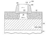
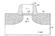
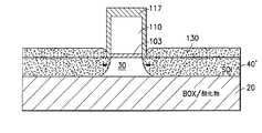
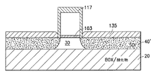
【解決手段】P型MOSFETは、ゲート110を絶縁体で封止し、ゲルマニウム含有層を側壁105の外側に成層させ、次いで、アニーリング又は酸化により、ゲルマニウムを絶縁体上シリコン層又はバルクシリコンの中に拡散させて、勾配付き組み込みシリコン−ゲルマニウムのソース−ドレイン40及び/又は延長部(geSiGe−SDE)を形成する。SOIデバイスにおいては、geSiGe−SDEは、水平方向の(ゲート誘電面に対して平行な)圧縮応力と、垂直方向の(該ゲート誘電面に対して直角の)引張り応力とをPMOSFETのチャネルに生成し、これによって、PMOSFET性能を向上させる構造を形成する。
【選択図】図1
Description
1)歪みシリコンは緩和SiGe上で成長されるものであり、したがって、デバイスの漏れを制御するのが困難である。
2)性能を向上させるために、ゲルマニウム濃度を30%以上にするという要求は、さらに、欠陥の密度を増加させる。
3)SiGeにおけるヒ素及びリンのようなドーパントの高い拡散率は、浅いp−n接合を形成するのを困難にする。サブミクロン又はディープ・サブミクロンのMOSFETにおいては、デバイスをスケーリングするのに浅い接合が要求される。
本発明の別の特徴は、ゲルマニウムによる垂直方向の完全な又は部分的な浸透によって、SOI層の中にSiGe領域を形成することである。
シリコンSOIウェハーで開始し、
ゲート酸化物(又はこれと等価のもの)を成長させ、
ポリゲート層を成層し(又は金属ゲートデバイスの金属を成層し)、
窒化物マスク層を成層し、
フォトレジスト、RIE窒化物、ポリ−Si(金属ゲートのためのRIE金属)及び酸化物を成層してパターン加工し、
薄い窒化物スペーサ(〜10ないし30nm)を形成し、
露出したシリコン上に、選択的にエピタキシャルSiGe(又はゲルマニウム)を形成し、
高温でアニールし、ゲルマニウムをSiデバイス層の中に拡散し、ゲルマニウム濃度を垂直方向及び水平方向に勾配付けするが、好ましくは、ゲルマニウムの濃度勾配形状がチャネル領域に入らないようにし、
ハロ注入、延長部注入、スペーサ形成、S/D注入、RTA、メタライゼーションを含んで、トランジスタを完成させる。
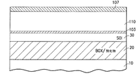
20:埋め込み絶縁体
30:SOI
40:ソース及びドレイン
100:電界効果トランジスタ
103:ゲート酸化物
105:側壁
107:ハードマスク
108:フォトレジスト
110:ゲート
130:エピタキシャル材料
Claims (25)
- PMOSFETを形成する方法であって、
埋め込み絶縁体層と前記埋め込み絶縁体層の上のSOI層とを有するSOIウェハーを準備し、
ゲート絶縁体層を前記SOI層の上方に形成し、
下側にチャネルを有するトランジスタゲートを前記SOI層の上に形成し、
絶縁体側壁を前記ゲートの第1の側面及び第2の側面に形成し、
ドーパントを含有するドーピング層を、前記SOI層上で前記絶縁体側壁に隣接してエピタキシャル形成し、
前記ドーパントを前記ドーピング層から前記SOI層の中に拡散させ、これによって、SOI表面に対して平行な水平方向の圧縮応力と、前記SOI表面に対して直角の垂直方向の引張り応力とを前記チャネルに生成し、
前記PMOSFETを完成させる、
ステップを含む方法。 - 前記拡散ステップが、高温アニールにより行われる請求項1に記載の方法。
- 前記ドーパントが前記SOI層の底面に到達するまで前記拡散ステップが継続される請求項1に記載の方法。
- 前記ドーパントが前記SOI層の底面に到達する前に前記拡散ステップが停止される請求項1に記載の方法。
- 前記ドーピング層がSiGeである請求項1に記載の方法。
- 前記ドーパント層が、原子番号20%より大きいゲルマニウム濃度をもつSiGeである請求項3に記載の方法。
- 熱酸化物の層を前記ドーピング層上に成長させ、これによって、該ドーピング層内の前記ドーパントを前記SOI層の中に拡散させるステップをさらに含む請求項1に記載の方法。
- 前記ドーパントを拡散させる前記ステップの後に、前記熱酸化物を除去するステップをさらに含む請求項7に記載の方法。
- 前記ドーパントが前記SOI層の底面に到達するまで前記拡散ステップが継続される請求項7に記載の方法。
- 前記ドーパントが前記SOI層の底面に到達する前に前記拡散ステップが停止される請求項7に記載の方法。
- 前記ドーピング層がSiGeである請求項7に記載の方法。
- 前記ドーピング層が、20%より大きいゲルマニウム濃度をもつSiGeである請求項11に記載の方法。
- PMOSFETを形成する方法であって、
バルクシリコンウェハーを準備し、
ゲート絶縁体層を前記バルクシリコンの上方に形成し、
下側にチャネルを有するトランジスタゲートを前記バルクシリコンの上に形成し、
絶縁体側壁を前記ゲートの第1の側面及び第2の側面に形成し、
ゲルマニウム又は不純物を含有するドーピング層を、前記バルクシリコン上で前記絶縁体側壁に隣接してエピタキシャル形成し、
ゲルマニウムを前記ゲルマニウムがドーピングされた層から前記バルクシリコンの中に拡散させ、これによって、(SOI表面に対して平行な)水平方向の圧縮応力と、(SOI表面に対して直角の)垂直方向の引張り応力とを前記チャネルに生成し、
前記PMOSFETを完成させる、
ステップを含む方法。 - 前記拡散ステップが、高温アニールにより行われる請求項13に記載の方法。
- 前記ドーピング層がSiGeである請求項13に記載の方法。
- 前記ドーパント層が、20%より大きいゲルマニウム濃度をもつSiGeである請求項13に記載の方法。
- 熱酸化物の層を前記ドーパント層上に成長させ、これによって、前記ドーパントを前記バルクシリコンの中に拡散させるステップをさらに含む請求項13に記載の方法。
- 前記ドーパントを拡散させる前記ステップの後に、前記熱酸化物を除去するステップをさらに含む請求項17に記載の方法。
- 前記ドーパント層がSiGeである請求項17に記載の方法。
- 前記ドーパント層が、20%より大きいゲルマニウム濃度をもつSiGeである請求項19に記載の方法。
- 埋め込み絶縁体層と前記埋め込み絶縁体層の上のSOI層とを有するSOIウェハーに形成された少なくとも1つのPMOSFETを含む集積回路であって、
前記少なくとも1つのPMOSFETが、前記SOI層の上方のゲート絶縁体と、該SOI層の上にあって下側にチャネルを有するトランジスタゲートとを有し、前記チャネルは、該チャネルにおいてSOI表面に対して平行な水平方向の圧縮応力と、前記SOI表面に対して直角の垂直方向の引張り応力とを有し、
前記SOI層が、前記水平方向の前記圧縮応力を生成するドーパントの濃度勾配を有し、前記ドーパントの前記濃度が、該SOI層の上面において最大値を有することを特徴とする集積回路。 - 前記ドーパントの濃度勾配が、前記SOI層の厚さより少ないドーパント深さまで延びる請求項21に記載の集積回路。
- 前記SOI層がシリコンであり、前記ドーパントがゲルマニウムである請求項22に記載の集積回路。
- 前記濃度勾配が高温アニールにより形成された請求項22に記載の集積回路。
- 前記濃度勾配が、前記SOI層の上に配設された成層ドーパント層を熱酸化することにより形成された請求項22に記載の集積回路。
Applications Claiming Priority (2)
| Application Number | Priority Date | Filing Date | Title |
|---|---|---|---|
| US10/710244 | 2004-06-29 | ||
| US10/710,244 US7288443B2 (en) | 2004-06-29 | 2004-06-29 | Structures and methods for manufacturing p-type MOSFET with graded embedded silicon-germanium source-drain and/or extension |
Publications (3)
| Publication Number | Publication Date |
|---|---|
| JP2006019727A true JP2006019727A (ja) | 2006-01-19 |
| JP2006019727A5 JP2006019727A5 (ja) | 2008-06-19 |
| JP5043314B2 JP5043314B2 (ja) | 2012-10-10 |
Family
ID=35504716
Family Applications (1)
| Application Number | Title | Priority Date | Filing Date |
|---|---|---|---|
| JP2005183624A Expired - Fee Related JP5043314B2 (ja) | 2004-06-29 | 2005-06-23 | 勾配付き組み込みシリコン−ゲルマニウムのソース−ドレイン及び/又は延長部をもつ、歪みp型mosfetを製造する方法 |
Country Status (4)
| Country | Link |
|---|---|
| US (1) | US7288443B2 (ja) |
| JP (1) | JP5043314B2 (ja) |
| CN (1) | CN100444336C (ja) |
| TW (1) | TW200625460A (ja) |
Cited By (4)
| Publication number | Priority date | Publication date | Assignee | Title |
|---|---|---|---|---|
| JP2008515188A (ja) * | 2004-09-29 | 2008-05-08 | フリースケール セミコンダクター インコーポレイテッド | 歪みチャネル、及びヘテロ接合ソース/ドレインを有する半導体素子を形成する方法 |
| JP2011044706A (ja) * | 2009-07-28 | 2011-03-03 | Taiwan Semiconductor Manufacturing Co Ltd | 高ゲルマニウム濃度のSiGeストレッサの形成方法 |
| WO2011030782A1 (ja) * | 2009-09-09 | 2011-03-17 | 学校法人神奈川大学 | 半導体素子構造の形成方法、及び半導体素子 |
| CN114514392A (zh) * | 2019-05-03 | 2022-05-17 | 泰普科英普罗有限责任公司 | 用于浮动阀座板的系统和方法 |
Families Citing this family (35)
| Publication number | Priority date | Publication date | Assignee | Title |
|---|---|---|---|---|
| US20060151808A1 (en) * | 2005-01-12 | 2006-07-13 | Chien-Hao Chen | MOSFET device with localized stressor |
| DE102005013982A1 (de) * | 2005-03-26 | 2006-10-05 | Atmel Germany Gmbh | Verfahren zur Herstellung eines Bipolartransistors und nach einem derartigen Verfahren hergestellter Bipolartransistor |
| US7439165B2 (en) * | 2005-04-06 | 2008-10-21 | Agency For Sceince, Technology And Reasearch | Method of fabricating tensile strained layers and compressive strain layers for a CMOS device |
| US7446350B2 (en) * | 2005-05-10 | 2008-11-04 | International Business Machine Corporation | Embedded silicon germanium using a double buried oxide silicon-on-insulator wafer |
| KR100675895B1 (ko) * | 2005-06-29 | 2007-02-02 | 주식회사 하이닉스반도체 | 반도체소자의 금속배선구조 및 그 제조방법 |
| EP1833094B1 (en) * | 2006-03-06 | 2011-02-02 | STMicroelectronics (Crolles 2) SAS | Formation of shallow SiGe conduction channel |
| CN100466255C (zh) * | 2006-04-18 | 2009-03-04 | 联华电子股份有限公司 | 半导体结构及其制作方法 |
| US8211761B2 (en) * | 2006-08-16 | 2012-07-03 | Globalfoundries Singapore Pte. Ltd. | Semiconductor system using germanium condensation |
| KR100773359B1 (ko) * | 2006-11-20 | 2007-11-05 | 삼성전자주식회사 | 높은 이동도를 갖는 트랜지스터들의 제조방법 및 그에 의해제조된 트랜지스터들 |
| US7696000B2 (en) | 2006-12-01 | 2010-04-13 | International Business Machines Corporation | Low defect Si:C layer with retrograde carbon profile |
| CN101295641B (zh) * | 2007-04-24 | 2010-09-29 | 中芯国际集成电路制造(上海)有限公司 | 栅极制造方法 |
| KR100844933B1 (ko) * | 2007-06-26 | 2008-07-09 | 주식회사 하이닉스반도체 | 반도체 소자의 트랜지스터 및 그 제조 방법 |
| US7709331B2 (en) * | 2007-09-07 | 2010-05-04 | Freescale Semiconductor, Inc. | Dual gate oxide device integration |
| US7704844B2 (en) * | 2007-10-04 | 2010-04-27 | International Business Machines Corporation | High performance MOSFET |
| US7964910B2 (en) | 2007-10-17 | 2011-06-21 | International Business Machines Corporation | Planar field effect transistor structure having an angled crystallographic etch-defined source/drain recess and a method of forming the transistor structure |
| CN101458337B (zh) * | 2007-12-12 | 2010-12-08 | 中国科学院微电子研究所 | 基于绝缘体上硅的双探头pmos辐射剂量计 |
| CN101937091B (zh) * | 2007-12-12 | 2012-07-25 | 中国科学院微电子研究所 | 一种可调整量程的堆叠测量电路 |
| US20090242989A1 (en) * | 2008-03-25 | 2009-10-01 | Chan Kevin K | Complementary metal-oxide-semiconductor device with embedded stressor |
| US7955909B2 (en) * | 2008-03-28 | 2011-06-07 | International Business Machines Corporation | Strained ultra-thin SOI transistor formed by replacement gate |
| FR2936095B1 (fr) * | 2008-09-18 | 2011-04-01 | Commissariat Energie Atomique | Procede de fabrication d'un dispositif microelectronique dote de zones semi-conductrices sur isolant a gradient horizontal de concentration en ge. |
| TWI416727B (zh) * | 2009-12-04 | 2013-11-21 | Inotera Memories Inc | P型金屬氧化層半導體場效電晶體及其製造方法 |
| CN102130054B (zh) * | 2010-01-20 | 2013-05-01 | 中芯国际集成电路制造(上海)有限公司 | 改善半导体器件的截止漏电流发散的方法 |
| CN102339852B (zh) | 2010-07-27 | 2013-03-27 | 中国科学院微电子研究所 | 半导体器件及其制造方法 |
| CN102569383A (zh) * | 2010-12-14 | 2012-07-11 | 中国科学院微电子研究所 | 一种mos管及其制造方法 |
| US20120161105A1 (en) * | 2010-12-22 | 2012-06-28 | Willy Rachmady | Uniaxially strained quantum well device and method of making same |
| DE102010064290B3 (de) * | 2010-12-28 | 2012-04-19 | GLOBALFOUNDRIES Dresden Module One Ltd. Liability Company & Co. KG | Verformungserhöhung in Transistoren mit einem eingebetteten verformungsinduzierenden Halbleitermaterial durch Kondensation der legierungsbildenden Substanz |
| CN102800594B (zh) * | 2011-05-26 | 2015-01-28 | 中芯国际集成电路制造(上海)有限公司 | Pmos管的制作方法 |
| CN102931082B (zh) * | 2011-08-10 | 2015-04-22 | 中芯国际集成电路制造(北京)有限公司 | 半导体器件及其制造方法 |
| US8735303B2 (en) * | 2011-11-02 | 2014-05-27 | Globalfoundries Inc. | Methods of forming PEET devices with different structures and performance characteristics |
| US8957476B2 (en) * | 2012-12-20 | 2015-02-17 | Intel Corporation | Conversion of thin transistor elements from silicon to silicon germanium |
| US9876110B2 (en) * | 2014-01-31 | 2018-01-23 | Stmicroelectronics, Inc. | High dose implantation for ultrathin semiconductor-on-insulator substrates |
| CN105679645A (zh) * | 2014-11-17 | 2016-06-15 | 上海华力微电子有限公司 | 嵌入式锗硅外延位错缺陷的改善方法 |
| US10043893B1 (en) | 2017-08-03 | 2018-08-07 | Globalfoundries Inc. | Post gate silicon germanium channel condensation and method for producing the same |
| CN112635325A (zh) * | 2020-12-07 | 2021-04-09 | 广东省大湾区集成电路与系统应用研究院 | 一种绝缘体上应变硅/锗晶体管及其制备方法 |
| CN113410309A (zh) * | 2021-06-23 | 2021-09-17 | 电子科技大学 | 一种低比导通电阻的分立栅mosfet器件及其制造方法 |
Citations (5)
| Publication number | Priority date | Publication date | Assignee | Title |
|---|---|---|---|---|
| JPH0982975A (ja) * | 1995-09-14 | 1997-03-28 | Toshiba Corp | 半導体装置およびその製造方法 |
| JPH1012883A (ja) * | 1996-06-20 | 1998-01-16 | Toshiba Corp | 半導体装置 |
| JPH1197673A (ja) * | 1997-09-17 | 1999-04-09 | Toshiba Corp | 半導体装置 |
| JP2003318198A (ja) * | 2002-04-25 | 2003-11-07 | Sanyo Electric Co Ltd | 半導体装置の製造方法 |
| WO2004081982A2 (en) * | 2003-03-07 | 2004-09-23 | Amberwave Systems Corporation | Shallow trench isolation process |
Family Cites Families (91)
| Publication number | Priority date | Publication date | Assignee | Title |
|---|---|---|---|---|
| US3602841A (en) | 1970-06-18 | 1971-08-31 | Ibm | High frequency bulk semiconductor amplifiers and oscillators |
| US4853076A (en) | 1983-12-29 | 1989-08-01 | Massachusetts Institute Of Technology | Semiconductor thin films |
| US4665415A (en) | 1985-04-24 | 1987-05-12 | International Business Machines Corporation | Semiconductor device with hole conduction via strained lattice |
| EP0219641B1 (de) | 1985-09-13 | 1991-01-09 | Siemens Aktiengesellschaft | Integrierte Bipolar- und komplementäre MOS-Transistoren auf einem gemeinsamen Substrat enthaltende Schaltung und Verfahren zu ihrer Herstellung |
| US4958213A (en) | 1987-12-07 | 1990-09-18 | Texas Instruments Incorporated | Method for forming a transistor base region under thick oxide |
| US5354695A (en) | 1992-04-08 | 1994-10-11 | Leedy Glenn J | Membrane dielectric isolation IC fabrication |
| US5459346A (en) | 1988-06-28 | 1995-10-17 | Ricoh Co., Ltd. | Semiconductor substrate with electrical contact in groove |
| US5006913A (en) | 1988-11-05 | 1991-04-09 | Mitsubishi Denki Kabushiki Kaisha | Stacked type semiconductor device |
| US5108843A (en) | 1988-11-30 | 1992-04-28 | Ricoh Company, Ltd. | Thin film semiconductor and process for producing the same |
| US4952524A (en) | 1989-05-05 | 1990-08-28 | At&T Bell Laboratories | Semiconductor device manufacture including trench formation |
| US5310446A (en) | 1990-01-10 | 1994-05-10 | Ricoh Company, Ltd. | Method for producing semiconductor film |
| US5060030A (en) | 1990-07-18 | 1991-10-22 | Raytheon Company | Pseudomorphic HEMT having strained compensation layer |
| US5081513A (en) | 1991-02-28 | 1992-01-14 | Xerox Corporation | Electronic device with recovery layer proximate to active layer |
| US5371399A (en) | 1991-06-14 | 1994-12-06 | International Business Machines Corporation | Compound semiconductor having metallic inclusions and devices fabricated therefrom |
| US5134085A (en) | 1991-11-21 | 1992-07-28 | Micron Technology, Inc. | Reduced-mask, split-polysilicon CMOS process, incorporating stacked-capacitor cells, for fabricating multi-megabit dynamic random access memories |
| US5391510A (en) | 1992-02-28 | 1995-02-21 | International Business Machines Corporation | Formation of self-aligned metal gate FETs using a benignant removable gate material during high temperature steps |
| US6008126A (en) | 1992-04-08 | 1999-12-28 | Elm Technology Corporation | Membrane dielectric isolation IC fabrication |
| US5561302A (en) | 1994-09-26 | 1996-10-01 | Motorola, Inc. | Enhanced mobility MOSFET device and method |
| US5679965A (en) | 1995-03-29 | 1997-10-21 | North Carolina State University | Integrated heterostructures of Group III-V nitride semiconductor materials including epitaxial ohmic contact, non-nitride buffer layer and methods of fabricating same |
| US5670798A (en) | 1995-03-29 | 1997-09-23 | North Carolina State University | Integrated heterostructures of Group III-V nitride semiconductor materials including epitaxial ohmic contact non-nitride buffer layer and methods of fabricating same |
| US5557122A (en) | 1995-05-12 | 1996-09-17 | Alliance Semiconductors Corporation | Semiconductor electrode having improved grain structure and oxide growth properties |
| KR100213196B1 (ko) | 1996-03-15 | 1999-08-02 | 윤종용 | 트렌치 소자분리 |
| US6403975B1 (en) | 1996-04-09 | 2002-06-11 | Max-Planck Gesellschaft Zur Forderung Der Wissenschafteneev | Semiconductor components, in particular photodetectors, light emitting diodes, optical modulators and waveguides with multilayer structures grown on silicon substrates |
| US5880040A (en) | 1996-04-15 | 1999-03-09 | Macronix International Co., Ltd. | Gate dielectric based on oxynitride grown in N2 O and annealed in NO |
| WO1998010523A1 (en) * | 1996-09-06 | 1998-03-12 | Philips Electronics N.V. | A zero-if receiver |
| US5861651A (en) | 1997-02-28 | 1999-01-19 | Lucent Technologies Inc. | Field effect devices and capacitors with improved thin film dielectrics and method for making same |
| US5940736A (en) | 1997-03-11 | 1999-08-17 | Lucent Technologies Inc. | Method for forming a high quality ultrathin gate oxide layer |
| US6309975B1 (en) | 1997-03-14 | 2001-10-30 | Micron Technology, Inc. | Methods of making implanted structures |
| US6025280A (en) | 1997-04-28 | 2000-02-15 | Lucent Technologies Inc. | Use of SiD4 for deposition of ultra thin and controllable oxides |
| US5960297A (en) | 1997-07-02 | 1999-09-28 | Kabushiki Kaisha Toshiba | Shallow trench isolation structure and method of forming the same |
| JP3139426B2 (ja) | 1997-10-15 | 2001-02-26 | 日本電気株式会社 | 半導体装置 |
| US6066545A (en) | 1997-12-09 | 2000-05-23 | Texas Instruments Incorporated | Birdsbeak encroachment using combination of wet and dry etch for isolation nitride |
| US6274421B1 (en) | 1998-01-09 | 2001-08-14 | Sharp Laboratories Of America, Inc. | Method of making metal gate sub-micron MOS transistor |
| KR100275908B1 (ko) | 1998-03-02 | 2000-12-15 | 윤종용 | 집적 회로에 트렌치 아이솔레이션을 형성하는방법 |
| US6165383A (en) | 1998-04-10 | 2000-12-26 | Organic Display Technology | Useful precursors for organic electroluminescent materials and devices made from such materials |
| US6361885B1 (en) | 1998-04-10 | 2002-03-26 | Organic Display Technology | Organic electroluminescent materials and device made from such materials |
| US5989978A (en) | 1998-07-16 | 1999-11-23 | Chartered Semiconductor Manufacturing, Ltd. | Shallow trench isolation of MOSFETS with reduced corner parasitic currents |
| JP4592837B2 (ja) | 1998-07-31 | 2010-12-08 | ルネサスエレクトロニクス株式会社 | 半導体装置の製造方法 |
| US6319794B1 (en) | 1998-10-14 | 2001-11-20 | International Business Machines Corporation | Structure and method for producing low leakage isolation devices |
| US6235598B1 (en) | 1998-11-13 | 2001-05-22 | Intel Corporation | Method of using thick first spacers to improve salicide resistance on polysilicon gates |
| US6117722A (en) | 1999-02-18 | 2000-09-12 | Taiwan Semiconductor Manufacturing Company | SRAM layout for relaxing mechanical stress in shallow trench isolation technology and method of manufacture thereof |
| US6255169B1 (en) | 1999-02-22 | 2001-07-03 | Advanced Micro Devices, Inc. | Process for fabricating a high-endurance non-volatile memory device |
| US6284626B1 (en) | 1999-04-06 | 2001-09-04 | Vantis Corporation | Angled nitrogen ion implantation for minimizing mechanical stress on side walls of an isolation trench |
| US6656822B2 (en) | 1999-06-28 | 2003-12-02 | Intel Corporation | Method for reduced capacitance interconnect system using gaseous implants into the ILD |
| US6228694B1 (en) | 1999-06-28 | 2001-05-08 | Intel Corporation | Method of increasing the mobility of MOS transistors by use of localized stress regions |
| US6281532B1 (en) | 1999-06-28 | 2001-08-28 | Intel Corporation | Technique to obtain increased channel mobilities in NMOS transistors by gate electrode engineering |
| US6362082B1 (en) | 1999-06-28 | 2002-03-26 | Intel Corporation | Methodology for control of short channel effects in MOS transistors |
| KR100332108B1 (ko) | 1999-06-29 | 2002-04-10 | 박종섭 | 반도체 소자의 트랜지스터 및 그 제조 방법 |
| TW426940B (en) | 1999-07-30 | 2001-03-21 | United Microelectronics Corp | Manufacturing method of MOS field effect transistor |
| US6483171B1 (en) | 1999-08-13 | 2002-11-19 | Micron Technology, Inc. | Vertical sub-micron CMOS transistors on (110), (111), (311), (511), and higher order surfaces of bulk, SOI and thin film structures and method of forming same |
| US6284623B1 (en) | 1999-10-25 | 2001-09-04 | Peng-Fei Zhang | Method of fabricating semiconductor devices using shallow trench isolation with reduced narrow channel effect |
| US6476462B2 (en) | 1999-12-28 | 2002-11-05 | Texas Instruments Incorporated | MOS-type semiconductor device and method for making same |
| US6221735B1 (en) | 2000-02-15 | 2001-04-24 | Philips Semiconductors, Inc. | Method for eliminating stress induced dislocations in CMOS devices |
| US6531369B1 (en) | 2000-03-01 | 2003-03-11 | Applied Micro Circuits Corporation | Heterojunction bipolar transistor (HBT) fabrication using a selectively deposited silicon germanium (SiGe) |
| US6368931B1 (en) | 2000-03-27 | 2002-04-09 | Intel Corporation | Thin tensile layers in shallow trench isolation and method of making same |
| US6493497B1 (en) | 2000-09-26 | 2002-12-10 | Motorola, Inc. | Electro-optic structure and process for fabricating same |
| US6501121B1 (en) | 2000-11-15 | 2002-12-31 | Motorola, Inc. | Semiconductor structure |
| US7312485B2 (en) | 2000-11-29 | 2007-12-25 | Intel Corporation | CMOS fabrication process utilizing special transistor orientation |
| US6563152B2 (en) | 2000-12-29 | 2003-05-13 | Intel Corporation | Technique to obtain high mobility channels in MOS transistors by forming a strain layer on an underside of a channel |
| US20020086497A1 (en) | 2000-12-30 | 2002-07-04 | Kwok Siang Ping | Beaker shape trench with nitride pull-back for STI |
| US6265317B1 (en) | 2001-01-09 | 2001-07-24 | Taiwan Semiconductor Manufacturing Company | Top corner rounding for shallow trench isolation |
| US6403486B1 (en) | 2001-04-30 | 2002-06-11 | Taiwan Semiconductor Manufacturing Company | Method for forming a shallow trench isolation |
| US6531740B2 (en) | 2001-07-17 | 2003-03-11 | Motorola, Inc. | Integrated impedance matching and stability network |
| US6498358B1 (en) | 2001-07-20 | 2002-12-24 | Motorola, Inc. | Structure and method for fabricating an electro-optic system having an electrochromic diffraction grating |
| US6908810B2 (en) | 2001-08-08 | 2005-06-21 | Taiwan Semiconductor Manufacturing Co., Ltd. | Method of preventing threshold voltage of MOS transistor from being decreased by shallow trench isolation formation |
| JP2003060076A (ja) | 2001-08-21 | 2003-02-28 | Nec Corp | 半導体装置及びその製造方法 |
| WO2003025984A2 (en) | 2001-09-21 | 2003-03-27 | Amberwave Systems Corporation | Semiconductor structures employing strained material layers with defined impurity gradients and methods for fabricating same |
| US20030057184A1 (en) | 2001-09-22 | 2003-03-27 | Shiuh-Sheng Yu | Method for pull back SiN to increase rounding effect in a shallow trench isolation process |
| US6656798B2 (en) | 2001-09-28 | 2003-12-02 | Infineon Technologies, Ag | Gate processing method with reduced gate oxide corner and edge thinning |
| US6621131B2 (en) * | 2001-11-01 | 2003-09-16 | Intel Corporation | Semiconductor transistor having a stressed channel |
| US6635506B2 (en) | 2001-11-07 | 2003-10-21 | International Business Machines Corporation | Method of fabricating micro-electromechanical switches on CMOS compatible substrates |
| US6461936B1 (en) | 2002-01-04 | 2002-10-08 | Infineon Technologies Ag | Double pullback method of filling an isolation trench |
| JP4173672B2 (ja) * | 2002-03-19 | 2008-10-29 | 株式会社ルネサステクノロジ | 半導体装置及びその製造方法 |
| US6621392B1 (en) | 2002-04-25 | 2003-09-16 | International Business Machines Corporation | Micro electromechanical switch having self-aligned spacers |
| US7388259B2 (en) * | 2002-11-25 | 2008-06-17 | International Business Machines Corporation | Strained finFET CMOS device structures |
| US6717216B1 (en) | 2002-12-12 | 2004-04-06 | International Business Machines Corporation | SOI based field effect transistor having a compressive film in undercut area under the channel and a method of making the device |
| US6825529B2 (en) | 2002-12-12 | 2004-11-30 | International Business Machines Corporation | Stress inducing spacers |
| US6974981B2 (en) | 2002-12-12 | 2005-12-13 | International Business Machines Corporation | Isolation structures for imposing stress patterns |
| US6900502B2 (en) * | 2003-04-03 | 2005-05-31 | Taiwan Semiconductor Manufacturing Company, Ltd. | Strained channel on insulator device |
| US6887798B2 (en) | 2003-05-30 | 2005-05-03 | International Business Machines Corporation | STI stress modification by nitrogen plasma treatment for improving performance in small width devices |
| US7279746B2 (en) | 2003-06-30 | 2007-10-09 | International Business Machines Corporation | High performance CMOS device structures and method of manufacture |
| US7119403B2 (en) | 2003-10-16 | 2006-10-10 | International Business Machines Corporation | High performance strained CMOS devices |
| US8008724B2 (en) | 2003-10-30 | 2011-08-30 | International Business Machines Corporation | Structure and method to enhance both nFET and pFET performance using different kinds of stressed layers |
| US6977194B2 (en) | 2003-10-30 | 2005-12-20 | International Business Machines Corporation | Structure and method to improve channel mobility by gate electrode stress modification |
| US7015082B2 (en) * | 2003-11-06 | 2006-03-21 | International Business Machines Corporation | High mobility CMOS circuits |
| US7122849B2 (en) | 2003-11-14 | 2006-10-17 | International Business Machines Corporation | Stressed semiconductor device structures having granular semiconductor material |
| US7247912B2 (en) | 2004-01-05 | 2007-07-24 | International Business Machines Corporation | Structures and methods for making strained MOSFETs |
| CA2454995C (en) * | 2004-01-07 | 2011-12-20 | Martinrea International Inc. | Method and apparatus for assembling and testing a fluid conduit |
| US7205206B2 (en) * | 2004-03-03 | 2007-04-17 | International Business Machines Corporation | Method of fabricating mobility enhanced CMOS devices |
| US7504693B2 (en) * | 2004-04-23 | 2009-03-17 | International Business Machines Corporation | Dislocation free stressed channels in bulk silicon and SOI CMOS devices by gate stress engineering |
| US7354806B2 (en) * | 2004-09-17 | 2008-04-08 | International Business Machines Corporation | Semiconductor device structure with active regions having different surface directions and methods |
-
2004
- 2004-06-29 US US10/710,244 patent/US7288443B2/en not_active Expired - Fee Related
-
2005
- 2005-06-21 CN CNB2005100789757A patent/CN100444336C/zh not_active Expired - Fee Related
- 2005-06-23 JP JP2005183624A patent/JP5043314B2/ja not_active Expired - Fee Related
- 2005-06-24 TW TW094121087A patent/TW200625460A/zh unknown
Patent Citations (5)
| Publication number | Priority date | Publication date | Assignee | Title |
|---|---|---|---|---|
| JPH0982975A (ja) * | 1995-09-14 | 1997-03-28 | Toshiba Corp | 半導体装置およびその製造方法 |
| JPH1012883A (ja) * | 1996-06-20 | 1998-01-16 | Toshiba Corp | 半導体装置 |
| JPH1197673A (ja) * | 1997-09-17 | 1999-04-09 | Toshiba Corp | 半導体装置 |
| JP2003318198A (ja) * | 2002-04-25 | 2003-11-07 | Sanyo Electric Co Ltd | 半導体装置の製造方法 |
| WO2004081982A2 (en) * | 2003-03-07 | 2004-09-23 | Amberwave Systems Corporation | Shallow trench isolation process |
Cited By (10)
| Publication number | Priority date | Publication date | Assignee | Title |
|---|---|---|---|---|
| JP2008515188A (ja) * | 2004-09-29 | 2008-05-08 | フリースケール セミコンダクター インコーポレイテッド | 歪みチャネル、及びヘテロ接合ソース/ドレインを有する半導体素子を形成する方法 |
| JP2011044706A (ja) * | 2009-07-28 | 2011-03-03 | Taiwan Semiconductor Manufacturing Co Ltd | 高ゲルマニウム濃度のSiGeストレッサの形成方法 |
| JP2014045208A (ja) * | 2009-07-28 | 2014-03-13 | Taiwan Semiconductor Manufactuaring Co Ltd | 集積回路のトランジスタ構造 |
| US9660082B2 (en) | 2009-07-28 | 2017-05-23 | Taiwan Semiconductor Manufacturing Company, Ltd. | Integrated circuit transistor structure with high germanium concentration SiGe stressor |
| JP2017147458A (ja) * | 2009-07-28 | 2017-08-24 | 台湾積體電路製造股▲ふん▼有限公司Taiwan Semiconductor Manufacturing Company,Ltd. | 集積回路のトランジスタ構造 |
| US10693003B2 (en) | 2009-07-28 | 2020-06-23 | Taiwan Semiconductor Manufacturing Company, Ltd. | Integrated circuit transistor structure with high germanium concentration SiGe stressor |
| WO2011030782A1 (ja) * | 2009-09-09 | 2011-03-17 | 学校法人神奈川大学 | 半導体素子構造の形成方法、及び半導体素子 |
| US8941092B2 (en) | 2009-09-09 | 2015-01-27 | Kanagawa University | Method for forming semiconductor device structure and semiconductor device |
| JP5700563B2 (ja) * | 2009-09-09 | 2015-04-15 | 学校法人神奈川大学 | 半導体素子構造の形成方法、及び半導体素子 |
| CN114514392A (zh) * | 2019-05-03 | 2022-05-17 | 泰普科英普罗有限责任公司 | 用于浮动阀座板的系统和方法 |
Also Published As
| Publication number | Publication date |
|---|---|
| JP5043314B2 (ja) | 2012-10-10 |
| US20050285192A1 (en) | 2005-12-29 |
| CN1716554A (zh) | 2006-01-04 |
| TW200625460A (en) | 2006-07-16 |
| CN100444336C (zh) | 2008-12-17 |
| US7288443B2 (en) | 2007-10-30 |
Similar Documents
| Publication | Publication Date | Title |
|---|---|---|
| JP5043314B2 (ja) | 勾配付き組み込みシリコン−ゲルマニウムのソース−ドレイン及び/又は延長部をもつ、歪みp型mosfetを製造する方法 | |
| US7413961B2 (en) | Method of fabricating a transistor structure | |
| US8912567B2 (en) | Strained channel transistor and method of fabrication thereof | |
| JP4847152B2 (ja) | 半導体装置とその製造方法 | |
| KR101811796B1 (ko) | 급경사 접합 프로파일을 갖는 소스/드레인 영역들을 구비하는 반도체 소자 및 그 제조방법 | |
| US7176481B2 (en) | In situ doped embedded sige extension and source/drain for enhanced PFET performance | |
| JP5091403B2 (ja) | 半導体装置およびその製造方法 | |
| US8796771B2 (en) | Creating anisotropically diffused junctions in field effect transistor devices | |
| JP5614184B2 (ja) | 半導体装置の製造方法 | |
| JPWO2008120335A1 (ja) | 半導体装置およびその製造方法 | |
| US20090001413A1 (en) | METHOD OF DOPING FIELD-EFFECT-TRANSISTORS (FETs) WITH REDUCED STRESS/STRAIN RELAXATION AND RESULTING FET DEVICES | |
| US8647939B2 (en) | Non-relaxed embedded stressors with solid source extension regions in CMOS devices | |
| US6696729B2 (en) | Semiconductor device having diffusion regions with different junction depths | |
| JP2003347399A (ja) | 半導体基板の製造方法 | |
| US7381624B2 (en) | Technique for forming a substrate having crystalline semiconductor regions of different characteristics located above a crystalline bulk substrate | |
| US7964921B2 (en) | MOSFET and production method of semiconductor device | |
| JP2006165480A (ja) | 半導体装置 | |
| US20110306170A1 (en) | Novel Method to Improve Performance by Enhancing Poly Gate Doping Concentration in an Embedded SiGe PMOS Process | |
| US7479422B2 (en) | Semiconductor device with stressors and method therefor | |
| US6323073B1 (en) | Method for forming doped regions on an SOI device | |
| US7951662B2 (en) | Method of fabricating strained silicon transistor | |
| CN109087859A (zh) | 一种半导体器件的制造方法 | |
| CN103137706A (zh) | 基于应变硅技术的深耗尽沟道晶体管 | |
| JP2009016423A (ja) | 半導体装置及びその製造方法 | |
| CN107437533B (zh) | 半导体结构及其制造方法 |
Legal Events
| Date | Code | Title | Description |
|---|---|---|---|
| A521 | Written amendment |
Free format text: JAPANESE INTERMEDIATE CODE: A523 Effective date: 20080423 |
|
| A621 | Written request for application examination |
Free format text: JAPANESE INTERMEDIATE CODE: A621 Effective date: 20080423 |
|
| RD03 | Notification of appointment of power of attorney |
Free format text: JAPANESE INTERMEDIATE CODE: A7423 Effective date: 20090206 |
|
| A977 | Report on retrieval |
Free format text: JAPANESE INTERMEDIATE CODE: A971007 Effective date: 20120126 |
|
| A131 | Notification of reasons for refusal |
Free format text: JAPANESE INTERMEDIATE CODE: A131 Effective date: 20120207 |
|
| A521 | Written amendment |
Free format text: JAPANESE INTERMEDIATE CODE: A523 Effective date: 20120420 |
|
| RD12 | Notification of acceptance of power of sub attorney |
Free format text: JAPANESE INTERMEDIATE CODE: A7432 Effective date: 20120420 |
|
| A521 | Written amendment |
Free format text: JAPANESE INTERMEDIATE CODE: A821 Effective date: 20120420 |
|
| TRDD | Decision of grant or rejection written | ||
| A01 | Written decision to grant a patent or to grant a registration (utility model) |
Free format text: JAPANESE INTERMEDIATE CODE: A01 Effective date: 20120626 |
|
| RD14 | Notification of resignation of power of sub attorney |
Free format text: JAPANESE INTERMEDIATE CODE: A7434 Effective date: 20120626 |
|
| A01 | Written decision to grant a patent or to grant a registration (utility model) |
Free format text: JAPANESE INTERMEDIATE CODE: A01 |
|
| A61 | First payment of annual fees (during grant procedure) |
Free format text: JAPANESE INTERMEDIATE CODE: A61 Effective date: 20120712 |
|
| R150 | Certificate of patent or registration of utility model |
Free format text: JAPANESE INTERMEDIATE CODE: R150 |
|
| FPAY | Renewal fee payment (event date is renewal date of database) |
Free format text: PAYMENT UNTIL: 20150720 Year of fee payment: 3 |
|
| R250 | Receipt of annual fees |
Free format text: JAPANESE INTERMEDIATE CODE: R250 |
|
| R250 | Receipt of annual fees |
Free format text: JAPANESE INTERMEDIATE CODE: R250 |
|
| LAPS | Cancellation because of no payment of annual fees |