JP2001168193A5 - - Google Patents
Download PDFInfo
- Publication number
- JP2001168193A5 JP2001168193A5 JP2000319053A JP2000319053A JP2001168193A5 JP 2001168193 A5 JP2001168193 A5 JP 2001168193A5 JP 2000319053 A JP2000319053 A JP 2000319053A JP 2000319053 A JP2000319053 A JP 2000319053A JP 2001168193 A5 JP2001168193 A5 JP 2001168193A5
- Authority
- JP
- Japan
- Prior art keywords
- layer
- silicon oxide
- low
- dielectric material
- carbon
- Prior art date
- Legal status (The legal status is an assumption and is not a legal conclusion. Google has not performed a legal analysis and makes no representation as to the accuracy of the status listed.)
- Granted
Links
Images


Description
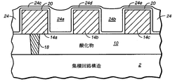
【請求項1】 近接して間隔を空けて離れた金属ラインを有する半導体基板上の集積回路構造の酸化物層上に低k酸化ケイ素誘電性材料の複合材層を形成するための方法であって、
該低k酸化ケイ素誘電性材料の複合材層は、近接して間隔を空けて離れた金属ライン間の高アスペクト比領域においてボイドフリー堆積性、及び標準k酸化ケイ素に匹敵する他の領域における堆積速度を呈し、バイア被毒特性を呈することがなく、
下記工程:
a)前記酸化物層及び前記金属ラインの上に、前記近接して間隔を空けて離れた金属ライン間の高アスペクト比領域においてボイドフリー堆積性を呈する低k酸化ケイ素誘電性材料の第一の層を、前記低k酸化ケイ素誘電性材料が前記酸化物層上の金属ラインのトップのレベルに達するまで、形成する工程、及び
b)前記第一の層よりも高い堆積速度で、前記第一の層の上に、低k酸化ケイ素誘電性材料の第二の層を形成する工程、
を含む方法。
【請求項17】 半導体基板上の集積回路構造の酸化物層上の低k炭素ドープ酸化ケイ素誘電性材料の複合材層であって、
該低k炭素ドープ酸化ケイ素誘電性材料の複合材層は、高アスペクト比領域においてボイドフリー堆積性、及び非炭素ドープ酸化ケイ素に匹敵する堆積速度を呈し、バイア被毒特性を呈することがなく、
下記:
a)炭素置換シラン反応物と過酸化水素との反応によって、低k炭素ドープ酸化ケイ素誘電性材料反応生成物の得られる堆積が前記酸化物層上の金属ラインのトップのレベルに達するまで形成される、低k炭素ドープ酸化ケイ素誘電性材料の第一の層;及び
b)前記第一の層の上に、プラズマエンハンスド化学蒸着(PECVD)によって、該低k炭素ドープ酸化ケイ素誘電性層の好適な厚み全体まで形成される、炭素ドープ低k酸化ケイ素誘電性材料の第二の層;
を含む複合材層。
Applications Claiming Priority (2)
| Application Number | Priority Date | Filing Date | Title |
|---|---|---|---|
| US09/426,056 US6391795B1 (en) | 1999-10-22 | 1999-10-22 | Low k dielectric composite layer for intergrated circuit structure which provides void-free low k dielectric material between metal lines while mitigating via poisoning |
| US09/426056 | 1999-10-22 |
Publications (3)
| Publication Number | Publication Date |
|---|---|
| JP2001168193A JP2001168193A (ja) | 2001-06-22 |
| JP2001168193A5 true JP2001168193A5 (ja) | 2007-11-22 |
| JP4731670B2 JP4731670B2 (ja) | 2011-07-27 |
Family
ID=23689100
Family Applications (1)
| Application Number | Title | Priority Date | Filing Date |
|---|---|---|---|
| JP2000319053A Expired - Fee Related JP4731670B2 (ja) | 1999-10-22 | 2000-10-19 | バイア被毒を緩和しつつ金属ライン間にボイドフリー低k誘電性材料を提供する集積回路構造のための低K誘電性複合材層 |
Country Status (3)
| Country | Link |
|---|---|
| US (2) | US6391795B1 (ja) |
| EP (1) | EP1094508B1 (ja) |
| JP (1) | JP4731670B2 (ja) |
Families Citing this family (28)
| Publication number | Priority date | Publication date | Assignee | Title |
|---|---|---|---|---|
| EP1035569B1 (en) * | 1997-11-27 | 2006-10-11 | Tokyo Electron Limited | Method for forming plasma films |
| US6268274B1 (en) * | 1999-10-14 | 2001-07-31 | Taiwan Semiconductor Manufacturing Company | Low temperature process for forming inter-metal gap-filling insulating layers in silicon wafer integrated circuitry |
| US6156743A (en) * | 1999-10-18 | 2000-12-05 | Whitcomb; John E. | Method of decreasing fatigue |
| US6762132B1 (en) * | 2000-08-31 | 2004-07-13 | Micron Technology, Inc. | Compositions for dissolution of low-K dielectric films, and methods of use |
| US6858195B2 (en) | 2001-02-23 | 2005-02-22 | Lsi Logic Corporation | Process for forming a low dielectric constant fluorine and carbon-containing silicon oxide dielectric material |
| US6572925B2 (en) * | 2001-02-23 | 2003-06-03 | Lsi Logic Corporation | Process for forming a low dielectric constant fluorine and carbon containing silicon oxide dielectric material |
| DE10134099A1 (de) * | 2001-07-13 | 2002-10-17 | Infineon Technologies Ag | Bedeckung von Leiterbahnen einer integrierten Halbleiterschaltung durch zwei Deckschichten |
| GB0118417D0 (en) * | 2001-07-28 | 2001-09-19 | Trikon Holdings Ltd | A method of depositing a dielectric film |
| US6632735B2 (en) * | 2001-08-07 | 2003-10-14 | Applied Materials, Inc. | Method of depositing low dielectric constant carbon doped silicon oxide |
| US20040033371A1 (en) * | 2002-05-16 | 2004-02-19 | Hacker Nigel P. | Deposition of organosilsesquioxane films |
| US6974762B2 (en) * | 2002-08-01 | 2005-12-13 | Intel Corporation | Adhesion of carbon doped oxides by silanization |
| US7005390B2 (en) * | 2002-10-09 | 2006-02-28 | Intel Corporation | Replenishment of surface carbon and surface passivation of low-k porous silicon-based dielectric materials |
| DE10249649A1 (de) * | 2002-10-24 | 2004-05-13 | Infineon Technologies Ag | Verfahren zur Herstellung einer flachen Grabenisolation |
| EP1435657A1 (en) * | 2002-12-30 | 2004-07-07 | STMicroelectronics S.r.l. | Non-volatile memory cell and manufacturing process |
| US20040248400A1 (en) * | 2003-06-09 | 2004-12-09 | Kim Sun-Oo | Composite low-k dielectric structure |
| CN100373530C (zh) * | 2004-05-11 | 2008-03-05 | 中芯国际集成电路制造(上海)有限公司 | 多孔膜的处理方法 |
| US7015150B2 (en) * | 2004-05-26 | 2006-03-21 | International Business Machines Corporation | Exposed pore sealing post patterning |
| KR100519170B1 (ko) * | 2004-07-13 | 2005-10-05 | 주식회사 하이닉스반도체 | 반도체 소자의 패시베이션막 형성방법 및 반도체 소자의패시베이션막 구조 |
| US20060038293A1 (en) * | 2004-08-23 | 2006-02-23 | Rueger Neal R | Inter-metal dielectric fill |
| US7393789B2 (en) * | 2005-09-01 | 2008-07-01 | Micron Technology, Inc. | Protective coating for planarization |
| US7923373B2 (en) | 2007-06-04 | 2011-04-12 | Micron Technology, Inc. | Pitch multiplication using self-assembling materials |
| US9245792B2 (en) * | 2008-07-25 | 2016-01-26 | Taiwan Semiconductor Manufacturing Company, Ltd. | Method for forming interconnect structures |
| US20100276764A1 (en) * | 2009-05-04 | 2010-11-04 | Yi-Jen Lo | Semiconductor structure with selectively deposited tungsten film and method for making the same |
| US8759234B2 (en) | 2011-10-17 | 2014-06-24 | Taiwan Semiconductor Manufacturing Company, Ltd. | Deposited material and method of formation |
| EP2662884B1 (en) * | 2012-05-09 | 2015-04-01 | Nxp B.V. | Group 13 nitride semiconductor device and method of its manufacture |
| US9230854B2 (en) | 2013-04-08 | 2016-01-05 | Taiwan Semiconductor Manufacturing Company, Ltd. | Semiconductor device and method |
| CN110148624A (zh) * | 2019-05-30 | 2019-08-20 | 上海华虹宏力半导体制造有限公司 | 半导体器件及其形成方法 |
| US11373947B2 (en) * | 2020-02-26 | 2022-06-28 | Taiwan Semiconductor Manufacturing Company, Ltd. | Methods of forming interconnect structures of semiconductor device |
Family Cites Families (65)
| Publication number | Priority date | Publication date | Assignee | Title |
|---|---|---|---|---|
| US3012861A (en) | 1960-01-15 | 1961-12-12 | Du Pont | Production of silicon |
| US3178392A (en) | 1962-04-09 | 1965-04-13 | Rohm & Haas | Heterocyclic and linear siliconmethylene and polysiloxane compounds containing siliconmethylene units and their preparation |
| US3652331A (en) | 1968-03-22 | 1972-03-28 | Shumpei Yamazaki | Process for forming a film on the surface of a substrate by a gas phase |
| US3920865A (en) | 1969-03-29 | 1975-11-18 | Degussa | Process of hydrophorizing highly dispersed metal or metalloid oxides |
| US3832202A (en) | 1972-08-08 | 1974-08-27 | Motorola Inc | Liquid silica source for semiconductors liquid silica source for semiconductors |
| US4771328A (en) | 1983-10-13 | 1988-09-13 | International Business Machine Corporation | Semiconductor device and process |
| JPS633437A (ja) | 1986-06-23 | 1988-01-08 | Sony Corp | 半導体装置の製造方法 |
| US4705725A (en) | 1986-11-28 | 1987-11-10 | E. I. Du Pont De Nemours And Company | Substrates with sterically-protected, stable, covalently-bonded organo-silane films |
| US5314845A (en) * | 1989-09-28 | 1994-05-24 | Applied Materials, Inc. | Two step process for forming void-free oxide layer over stepped surface of semiconductor wafer |
| JP2874297B2 (ja) | 1989-12-18 | 1999-03-24 | 東ソー株式会社 | 逆相クロマトグラフィー用充填剤及びその製造方法 |
| JPH0677402A (ja) | 1992-07-02 | 1994-03-18 | Natl Semiconductor Corp <Ns> | 半導体デバイス用誘電体構造及びその製造方法 |
| CA2137928C (en) | 1992-07-04 | 2002-01-29 | Christopher David Dobson | A method of treating a semiconductor wafer |
| US5580429A (en) | 1992-08-25 | 1996-12-03 | Northeastern University | Method for the deposition and modification of thin films using a combination of vacuum arcs and plasma immersion ion implantation |
| US5376595A (en) | 1992-08-28 | 1994-12-27 | Allied-Signal Inc. | Silicon carboxide ceramics from spirosiloxanes |
| US5302233A (en) * | 1993-03-19 | 1994-04-12 | Micron Semiconductor, Inc. | Method for shaping features of a semiconductor structure using chemical mechanical planarization (CMP) |
| US5364800A (en) | 1993-06-24 | 1994-11-15 | Texas Instruments Incorporated | Varying the thickness of the surface silicon layer in a silicon-on-insulator substrate |
| US5470801A (en) | 1993-06-28 | 1995-11-28 | Lsi Logic Corporation | Low dielectric constant insulation layer for integrated circuit structure and method of making same |
| JP3391410B2 (ja) | 1993-09-17 | 2003-03-31 | 富士通株式会社 | レジストマスクの除去方法 |
| US5558718A (en) | 1994-04-08 | 1996-09-24 | The Regents, University Of California | Pulsed source ion implantation apparatus and method |
| JPH07288253A (ja) * | 1994-04-18 | 1995-10-31 | Kawasaki Steel Corp | 絶縁膜の平坦化方法 |
| US5559367A (en) | 1994-07-12 | 1996-09-24 | International Business Machines Corporation | Diamond-like carbon for use in VLSI and ULSI interconnect systems |
| US5625232A (en) | 1994-07-15 | 1997-04-29 | Texas Instruments Incorporated | Reliability of metal leads in high speed LSI semiconductors using dummy vias |
| US5494854A (en) * | 1994-08-17 | 1996-02-27 | Texas Instruments Incorporated | Enhancement in throughput and planarity during CMP using a dielectric stack containing HDP-SiO2 films |
| JPH08172132A (ja) * | 1994-09-15 | 1996-07-02 | Texas Instr Inc <Ti> | マルチレベル相互接続部の容量および性能を最適化する素子および方法 |
| JPH08162528A (ja) * | 1994-10-03 | 1996-06-21 | Sony Corp | 半導体装置の層間絶縁膜構造 |
| US5821621A (en) * | 1995-10-12 | 1998-10-13 | Texas Instruments Incorporated | Low capacitance interconnect structure for integrated circuits |
| KR100209365B1 (ko) | 1995-11-01 | 1999-07-15 | 김영환 | 에스.오.아이 반도체 웨이퍼의 제조방법 |
| JPH09237785A (ja) * | 1995-12-28 | 1997-09-09 | Toshiba Corp | 半導体装置およびその製造方法 |
| US5882489A (en) | 1996-04-26 | 1999-03-16 | Ulvac Technologies, Inc. | Processes for cleaning and stripping photoresist from surfaces of semiconductor wafers |
| TW391048B (en) * | 1996-04-29 | 2000-05-21 | Texas Instruments Inc | Intergrated circuit insulator and method |
| JP3186998B2 (ja) * | 1996-06-03 | 2001-07-11 | 日本電気株式会社 | 半導体装置および半導体装置の製造方法 |
| JP3355949B2 (ja) * | 1996-08-16 | 2002-12-09 | 日本電気株式会社 | プラズマcvd絶縁膜の形成方法 |
| US5989998A (en) * | 1996-08-29 | 1999-11-23 | Matsushita Electric Industrial Co., Ltd. | Method of forming interlayer insulating film |
| US5939763A (en) | 1996-09-05 | 1999-08-17 | Advanced Micro Devices, Inc. | Ultrathin oxynitride structure and process for VLSI applications |
| KR100205318B1 (ko) | 1996-10-11 | 1999-07-01 | 구본준 | 자유전율의 절연막 제조방법 |
| JP3402972B2 (ja) * | 1996-11-14 | 2003-05-06 | 東京エレクトロン株式会社 | 半導体装置の製造方法 |
| US5953635A (en) * | 1996-12-19 | 1999-09-14 | Intel Corporation | Interlayer dielectric with a composite dielectric stack |
| US5913140A (en) * | 1996-12-23 | 1999-06-15 | Lam Research Corporation | Method for reduction of plasma charging damage during chemical vapor deposition |
| JPH10242143A (ja) * | 1997-02-27 | 1998-09-11 | Mitsubishi Electric Corp | 半導体装置、半導体装置の製造方法及び半導体装置の絶縁膜形成方法 |
| US5818111A (en) * | 1997-03-21 | 1998-10-06 | Texas Instruments Incorporated | Low capacitance interconnect structures in integrated circuits using a stack of low dielectric materials |
| US5858879A (en) | 1997-06-06 | 1999-01-12 | Taiwan Semiconductor Manufacturing Co., Ltd. | Method for etching metal lines with enhanced profile control |
| US5915203A (en) * | 1997-06-10 | 1999-06-22 | Vlsi Technology, Inc. | Method for producing deep submicron interconnect vias |
| US6037248A (en) | 1997-06-13 | 2000-03-14 | Micron Technology, Inc. | Method of fabricating integrated circuit wiring with low RC time delay |
| JPH1116904A (ja) * | 1997-06-26 | 1999-01-22 | Mitsubishi Electric Corp | 半導体装置及びその製造方法 |
| DE19804375B4 (de) * | 1997-06-26 | 2005-05-19 | Mitsubishi Denki K.K. | Verfahren zur Herstellung eines Zwischenschichtisolierfilmes |
| US6025263A (en) | 1997-07-15 | 2000-02-15 | Nanya Technology Corporation | Underlayer process for high O3 /TEOS interlayer dielectric deposition |
| US5904154A (en) | 1997-07-24 | 1999-05-18 | Vanguard International Semiconductor Corporation | Method for removing fluorinated photoresist layers from semiconductor substrates |
| US6207005B1 (en) | 1997-07-29 | 2001-03-27 | Silicon Genesis Corporation | Cluster tool apparatus using plasma immersion ion implantation |
| US5874745A (en) | 1997-08-05 | 1999-02-23 | International Business Machines Corporation | Thin film transistor with carbonaceous gate dielectric |
| JPH1197533A (ja) * | 1997-09-22 | 1999-04-09 | Hitachi Ltd | 半導体集積回路及びその製造方法 |
| JP3211950B2 (ja) * | 1998-01-19 | 2001-09-25 | 日本電気株式会社 | 半導体装置およびその製造方法 |
| US6348421B1 (en) * | 1998-02-06 | 2002-02-19 | National Semiconductor Corporation | Dielectric gap fill process that effectively reduces capacitance between narrow metal lines using HDP-CVD |
| US6051073A (en) | 1998-02-11 | 2000-04-18 | Silicon Genesis Corporation | Perforated shield for plasma immersion ion implantation |
| US6054379A (en) * | 1998-02-11 | 2000-04-25 | Applied Materials, Inc. | Method of depositing a low k dielectric with organo silane |
| US6303523B2 (en) | 1998-02-11 | 2001-10-16 | Applied Materials, Inc. | Plasma processes for depositing low dielectric constant films |
| JP3305251B2 (ja) * | 1998-02-26 | 2002-07-22 | 松下電器産業株式会社 | 配線構造体の形成方法 |
| JP3189781B2 (ja) | 1998-04-08 | 2001-07-16 | 日本電気株式会社 | 半導体装置の製造方法 |
| US6066574A (en) | 1998-11-06 | 2000-05-23 | Advanced Micro Devices, Inc. | Hot plate cure process for BCB low k interlevel dielectric |
| JP4454713B2 (ja) | 1999-03-17 | 2010-04-21 | 株式会社半導体エネルギー研究所 | 半導体装置及びその作製方法 |
| US6303047B1 (en) | 1999-03-22 | 2001-10-16 | Lsi Logic Corporation | Low dielectric constant multiple carbon-containing silicon oxide dielectric material for use in integrated circuit structures, and method of making same |
| US6204192B1 (en) | 1999-03-29 | 2001-03-20 | Lsi Logic Corporation | Plasma cleaning process for openings formed in at least one low dielectric constant insulation layer over copper metallization in integrated circuit structures |
| US6028015A (en) | 1999-03-29 | 2000-02-22 | Lsi Logic Corporation | Process for treating damaged surfaces of low dielectric constant organo silicon oxide insulation material to inhibit moisture absorption |
| US6232658B1 (en) | 1999-06-30 | 2001-05-15 | Lsi Logic Corporation | Process to prevent stress cracking of dielectric films on semiconductor wafers |
| US6114259A (en) | 1999-07-27 | 2000-09-05 | Lsi Logic Corporation | Process for treating exposed surfaces of a low dielectric constant carbon doped silicon oxide dielectric material to protect the material from damage |
| US6147012A (en) | 1999-11-12 | 2000-11-14 | Lsi Logic Corporation | Process for forming low k silicon oxide dielectric material while suppressing pressure spiking and inhibiting increase in dielectric constant |
-
1999
- 1999-10-22 US US09/426,056 patent/US6391795B1/en not_active Expired - Lifetime
-
2000
- 2000-10-18 EP EP00122684.4A patent/EP1094508B1/en not_active Expired - Lifetime
- 2000-10-19 JP JP2000319053A patent/JP4731670B2/ja not_active Expired - Fee Related
-
2002
- 2002-03-15 US US10/099,641 patent/US6800940B2/en not_active Expired - Lifetime
Similar Documents
| Publication | Publication Date | Title |
|---|---|---|
| JP2001168193A5 (ja) | ||
| TW554436B (en) | Carbon-graded layer for improved adhesion of low-k dielectrics to silicon substrates | |
| US7239017B1 (en) | Low-k B-doped SiC copper diffusion barrier films | |
| US7420275B1 (en) | Boron-doped SIC copper diffusion barrier films | |
| US7573061B1 (en) | Low-k SiC copper diffusion barrier films | |
| US6417092B1 (en) | Low dielectric constant etch stop films | |
| JP4731670B2 (ja) | バイア被毒を緩和しつつ金属ライン間にボイドフリー低k誘電性材料を提供する集積回路構造のための低K誘電性複合材層 | |
| CN102237272B (zh) | 半导体装置和半导体装置制造方法 | |
| KR20010076361A (ko) | 기질상에 필름을 형성하는 방법 및 장치 | |
| JP2003188254A5 (ja) | ||
| KR100817350B1 (ko) | 규소 탄화물 박막의 이중 플라즈마 처리 | |
| TW557478B (en) | Semiconductor device and manufacturing method thereof | |
| TWI272694B (en) | Metal ion diffusion barrier layers | |
| JP2000277515A (ja) | 層間絶縁膜の形成方法、化学的気相成長装置、及び半導体装置 | |
| JP3430114B2 (ja) | 改良された低誘電率の炭素−含有酸化ケイ素誘電体の形成方法 | |
| JPH10163192A (ja) | 半導体装置およびその製造方法 | |
| JP3476409B2 (ja) | プラズマcvd装置 | |
| US9728480B2 (en) | Passivation layer and method of making a passivation layer | |
| JP2004507103A (ja) | ライナー酸化物にmsq材料を結合する方法及び構造 | |
| TWI226100B (en) | Improved fluorine doped SiO2 film and method of fabrication | |
| US9368448B2 (en) | Metal-containing films as dielectric capping barrier for advanced interconnects | |
| JP2000286252A (ja) | 半導体装置の製造方法 | |
| JP2000223485A (ja) | 複合絶縁膜の製造方法及びこれを用いた半導体装置の製造方法 | |
| US20240026527A1 (en) | Method of depositing silicon based dielectric film | |
| TW493220B (en) | Method for improving adhesion between carbon doped oxide layer and thin film layer |