EP3690385B1 - Dehnungsmesser und sensormodul - Google Patents
Dehnungsmesser und sensormodul Download PDFInfo
- Publication number
- EP3690385B1 EP3690385B1 EP18860610.7A EP18860610A EP3690385B1 EP 3690385 B1 EP3690385 B1 EP 3690385B1 EP 18860610 A EP18860610 A EP 18860610A EP 3690385 B1 EP3690385 B1 EP 3690385B1
- Authority
- EP
- European Patent Office
- Prior art keywords
- resistor
- strain gauge
- layer
- substrate
- metallic layer
- Prior art date
- Legal status (The legal status is an assumption and is not a legal conclusion. Google has not performed a legal analysis and makes no representation as to the accuracy of the status listed.)
- Active
Links
- 239000010410 layer Substances 0.000 claims description 201
- 239000000758 substrate Substances 0.000 claims description 112
- 239000000463 material Substances 0.000 claims description 63
- 239000011651 chromium Substances 0.000 claims description 62
- 239000002346 layers by function Substances 0.000 claims description 59
- PXHVJJICTQNCMI-UHFFFAOYSA-N Nickel Chemical compound [Ni] PXHVJJICTQNCMI-UHFFFAOYSA-N 0.000 claims description 32
- 229920005989 resin Polymers 0.000 claims description 25
- 239000011347 resin Substances 0.000 claims description 25
- 239000002131 composite material Substances 0.000 claims description 24
- 239000010936 titanium Substances 0.000 claims description 21
- 239000010949 copper Substances 0.000 claims description 19
- 229910052804 chromium Inorganic materials 0.000 claims description 16
- 229910000881 Cu alloy Inorganic materials 0.000 claims description 11
- 229910000990 Ni alloy Inorganic materials 0.000 claims description 11
- 229910000679 solder Inorganic materials 0.000 claims description 11
- 239000013078 crystal Substances 0.000 claims description 8
- 229910052751 metal Inorganic materials 0.000 claims description 8
- 239000002184 metal Substances 0.000 claims description 8
- NRTOMJZYCJJWKI-UHFFFAOYSA-N Titanium nitride Chemical compound [Ti]#N NRTOMJZYCJJWKI-UHFFFAOYSA-N 0.000 claims description 5
- 229910045601 alloy Inorganic materials 0.000 claims description 4
- 239000000956 alloy Substances 0.000 claims description 4
- 230000001737 promoting effect Effects 0.000 claims description 4
- 229910052719 titanium Inorganic materials 0.000 claims description 4
- RYGMFSIKBFXOCR-UHFFFAOYSA-N Copper Chemical compound [Cu] RYGMFSIKBFXOCR-UHFFFAOYSA-N 0.000 claims description 3
- RTAQQCXQSZGOHL-UHFFFAOYSA-N Titanium Chemical compound [Ti] RTAQQCXQSZGOHL-UHFFFAOYSA-N 0.000 claims description 3
- 229910052802 copper Inorganic materials 0.000 claims description 3
- 229910000570 Cupronickel Inorganic materials 0.000 claims description 2
- 150000002736 metal compounds Chemical class 0.000 claims description 2
- 238000000034 method Methods 0.000 description 53
- 239000010408 film Substances 0.000 description 49
- 230000008569 process Effects 0.000 description 36
- 238000004090 dissolution Methods 0.000 description 27
- 238000001465 metallisation Methods 0.000 description 27
- 238000010438 heat treatment Methods 0.000 description 17
- 238000010586 diagram Methods 0.000 description 16
- 238000004519 manufacturing process Methods 0.000 description 16
- 230000004048 modification Effects 0.000 description 16
- 238000012986 modification Methods 0.000 description 16
- 239000000945 filler Substances 0.000 description 14
- 239000010931 gold Substances 0.000 description 13
- BASFCYQUMIYNBI-UHFFFAOYSA-N platinum Substances [Pt] BASFCYQUMIYNBI-UHFFFAOYSA-N 0.000 description 10
- 239000012790 adhesive layer Substances 0.000 description 9
- 238000001755 magnetron sputter deposition Methods 0.000 description 9
- 229920001721 polyimide Polymers 0.000 description 9
- 230000000052 comparative effect Effects 0.000 description 8
- 238000009713 electroplating Methods 0.000 description 8
- 229910052759 nickel Inorganic materials 0.000 description 8
- 239000009719 polyimide resin Substances 0.000 description 8
- 230000000694 effects Effects 0.000 description 7
- KDLHZDBZIXYQEI-UHFFFAOYSA-N palladium Substances [Pd] KDLHZDBZIXYQEI-UHFFFAOYSA-N 0.000 description 6
- 238000004544 sputter deposition Methods 0.000 description 6
- VYZAMTAEIAYCRO-UHFFFAOYSA-N Chromium Chemical compound [Cr] VYZAMTAEIAYCRO-UHFFFAOYSA-N 0.000 description 5
- 230000002411 adverse Effects 0.000 description 5
- 238000007772 electroless plating Methods 0.000 description 5
- 229910052737 gold Inorganic materials 0.000 description 5
- 230000003647 oxidation Effects 0.000 description 5
- 238000007254 oxidation reaction Methods 0.000 description 5
- 229910052697 platinum Inorganic materials 0.000 description 5
- 238000005476 soldering Methods 0.000 description 5
- 239000004696 Poly ether ether ketone Substances 0.000 description 4
- VYPSYNLAJGMNEJ-UHFFFAOYSA-N Silicium dioxide Chemical compound O=[Si]=O VYPSYNLAJGMNEJ-UHFFFAOYSA-N 0.000 description 4
- 239000003822 epoxy resin Substances 0.000 description 4
- XEEYBQQBJWHFJM-UHFFFAOYSA-N iron Substances [Fe] XEEYBQQBJWHFJM-UHFFFAOYSA-N 0.000 description 4
- 238000000206 photolithography Methods 0.000 description 4
- 229920000647 polyepoxide Polymers 0.000 description 4
- 229920002530 polyetherether ketone Polymers 0.000 description 4
- 239000002994 raw material Substances 0.000 description 4
- IJGRMHOSHXDMSA-UHFFFAOYSA-N Atomic nitrogen Chemical compound N#N IJGRMHOSHXDMSA-UHFFFAOYSA-N 0.000 description 3
- 239000004734 Polyphenylene sulfide Substances 0.000 description 3
- 238000002441 X-ray diffraction Methods 0.000 description 3
- QVGXLLKOCUKJST-UHFFFAOYSA-N atomic oxygen Chemical compound [O] QVGXLLKOCUKJST-UHFFFAOYSA-N 0.000 description 3
- 230000008859 change Effects 0.000 description 3
- 150000001875 compounds Chemical class 0.000 description 3
- 238000000151 deposition Methods 0.000 description 3
- -1 for example Substances 0.000 description 3
- 239000007789 gas Substances 0.000 description 3
- 238000009413 insulation Methods 0.000 description 3
- 239000001301 oxygen Substances 0.000 description 3
- 229910052760 oxygen Inorganic materials 0.000 description 3
- 229920003207 poly(ethylene-2,6-naphthalate) Polymers 0.000 description 3
- 239000011112 polyethylene naphthalate Substances 0.000 description 3
- 229920000139 polyethylene terephthalate Polymers 0.000 description 3
- 239000005020 polyethylene terephthalate Substances 0.000 description 3
- 229920000069 polyphenylene sulfide Polymers 0.000 description 3
- 238000005546 reactive sputtering Methods 0.000 description 3
- 229910052710 silicon Inorganic materials 0.000 description 3
- 229920002050 silicone resin Polymers 0.000 description 3
- XKRFYHLGVUSROY-UHFFFAOYSA-N Argon Chemical compound [Ar] XKRFYHLGVUSROY-UHFFFAOYSA-N 0.000 description 2
- 229910018487 Ni—Cr Inorganic materials 0.000 description 2
- GWEVSGVZZGPLCZ-UHFFFAOYSA-N Titan oxide Chemical compound O=[Ti]=O GWEVSGVZZGPLCZ-UHFFFAOYSA-N 0.000 description 2
- 229910052782 aluminium Inorganic materials 0.000 description 2
- 230000001668 ameliorated effect Effects 0.000 description 2
- 238000004458 analytical method Methods 0.000 description 2
- 238000005229 chemical vapour deposition Methods 0.000 description 2
- VNNRSPGTAMTISX-UHFFFAOYSA-N chromium nickel Chemical compound [Cr].[Ni] VNNRSPGTAMTISX-UHFFFAOYSA-N 0.000 description 2
- 230000007797 corrosion Effects 0.000 description 2
- 238000005260 corrosion Methods 0.000 description 2
- 238000005520 cutting process Methods 0.000 description 2
- 230000006866 deterioration Effects 0.000 description 2
- 230000007613 environmental effect Effects 0.000 description 2
- 238000011156 evaluation Methods 0.000 description 2
- PCHJSUWPFVWCPO-UHFFFAOYSA-N gold Chemical compound [Au] PCHJSUWPFVWCPO-UHFFFAOYSA-N 0.000 description 2
- 238000000227 grinding Methods 0.000 description 2
- 230000006872 improvement Effects 0.000 description 2
- 239000012535 impurity Substances 0.000 description 2
- 238000007733 ion plating Methods 0.000 description 2
- 230000001678 irradiating effect Effects 0.000 description 2
- WABPQHHGFIMREM-UHFFFAOYSA-N lead(0) Chemical compound [Pb] WABPQHHGFIMREM-UHFFFAOYSA-N 0.000 description 2
- 239000007788 liquid Substances 0.000 description 2
- 239000011572 manganese Substances 0.000 description 2
- 150000002739 metals Chemical class 0.000 description 2
- 239000010955 niobium Substances 0.000 description 2
- 230000003287 optical effect Effects 0.000 description 2
- 238000000059 patterning Methods 0.000 description 2
- 238000007517 polishing process Methods 0.000 description 2
- 229920005672 polyolefin resin Polymers 0.000 description 2
- 238000003825 pressing Methods 0.000 description 2
- 238000004549 pulsed laser deposition Methods 0.000 description 2
- 230000009467 reduction Effects 0.000 description 2
- 239000010948 rhodium Substances 0.000 description 2
- 238000007790 scraping Methods 0.000 description 2
- 238000007789 sealing Methods 0.000 description 2
- 239000000377 silicon dioxide Substances 0.000 description 2
- 239000002344 surface layer Substances 0.000 description 2
- 229910052715 tantalum Inorganic materials 0.000 description 2
- 229920002803 thermoplastic polyurethane Polymers 0.000 description 2
- 229920001187 thermosetting polymer Polymers 0.000 description 2
- 229910052721 tungsten Inorganic materials 0.000 description 2
- 238000007740 vapor deposition Methods 0.000 description 2
- XLYOFNOQVPJJNP-UHFFFAOYSA-N water Substances O XLYOFNOQVPJJNP-UHFFFAOYSA-N 0.000 description 2
- 238000001039 wet etching Methods 0.000 description 2
- 239000011701 zinc Substances 0.000 description 2
- OKTJSMMVPCPJKN-UHFFFAOYSA-N Carbon Chemical compound [C] OKTJSMMVPCPJKN-UHFFFAOYSA-N 0.000 description 1
- 229910002482 Cu–Ni Inorganic materials 0.000 description 1
- 229910002555 FeNi Inorganic materials 0.000 description 1
- 229910000604 Ferrochrome Inorganic materials 0.000 description 1
- PWHULOQIROXLJO-UHFFFAOYSA-N Manganese Chemical compound [Mn] PWHULOQIROXLJO-UHFFFAOYSA-N 0.000 description 1
- ZOKXTWBITQBERF-UHFFFAOYSA-N Molybdenum Chemical compound [Mo] ZOKXTWBITQBERF-UHFFFAOYSA-N 0.000 description 1
- KJTLSVCANCCWHF-UHFFFAOYSA-N Ruthenium Chemical compound [Ru] KJTLSVCANCCWHF-UHFFFAOYSA-N 0.000 description 1
- 229910052581 Si3N4 Inorganic materials 0.000 description 1
- 229910004166 TaN Inorganic materials 0.000 description 1
- 229910010038 TiAl Inorganic materials 0.000 description 1
- WGLPBDUCMAPZCE-UHFFFAOYSA-N Trioxochromium Chemical compound O=[Cr](=O)=O WGLPBDUCMAPZCE-UHFFFAOYSA-N 0.000 description 1
- HCHKCACWOHOZIP-UHFFFAOYSA-N Zinc Chemical compound [Zn] HCHKCACWOHOZIP-UHFFFAOYSA-N 0.000 description 1
- QCWXUUIWCKQGHC-UHFFFAOYSA-N Zirconium Chemical compound [Zr] QCWXUUIWCKQGHC-UHFFFAOYSA-N 0.000 description 1
- 230000001133 acceleration Effects 0.000 description 1
- 230000004075 alteration Effects 0.000 description 1
- XAGFODPZIPBFFR-UHFFFAOYSA-N aluminium Chemical compound [Al] XAGFODPZIPBFFR-UHFFFAOYSA-N 0.000 description 1
- PNEYBMLMFCGWSK-UHFFFAOYSA-N aluminium oxide Inorganic materials [O-2].[O-2].[O-2].[Al+3].[Al+3] PNEYBMLMFCGWSK-UHFFFAOYSA-N 0.000 description 1
- 229910052786 argon Inorganic materials 0.000 description 1
- 230000005540 biological transmission Effects 0.000 description 1
- 230000015572 biosynthetic process Effects 0.000 description 1
- 229910052797 bismuth Inorganic materials 0.000 description 1
- JCXGWMGPZLAOME-UHFFFAOYSA-N bismuth atom Chemical compound [Bi] JCXGWMGPZLAOME-UHFFFAOYSA-N 0.000 description 1
- 229910052799 carbon Inorganic materials 0.000 description 1
- 229910000423 chromium oxide Inorganic materials 0.000 description 1
- 229910017052 cobalt Inorganic materials 0.000 description 1
- 239000010941 cobalt Substances 0.000 description 1
- GUTLYIVDDKVIGB-UHFFFAOYSA-N cobalt atom Chemical compound [Co] GUTLYIVDDKVIGB-UHFFFAOYSA-N 0.000 description 1
- 229910052681 coesite Inorganic materials 0.000 description 1
- 239000000805 composite resin Substances 0.000 description 1
- YOCUPQPZWBBYIX-UHFFFAOYSA-N copper nickel Chemical compound [Ni].[Cu] YOCUPQPZWBBYIX-UHFFFAOYSA-N 0.000 description 1
- 229910052906 cristobalite Inorganic materials 0.000 description 1
- 230000001419 dependent effect Effects 0.000 description 1
- 230000008021 deposition Effects 0.000 description 1
- 230000002542 deteriorative effect Effects 0.000 description 1
- 238000009792 diffusion process Methods 0.000 description 1
- 229910001873 dinitrogen Inorganic materials 0.000 description 1
- 238000005530 etching Methods 0.000 description 1
- 229910052735 hafnium Inorganic materials 0.000 description 1
- VBJZVLUMGGDVMO-UHFFFAOYSA-N hafnium atom Chemical compound [Hf] VBJZVLUMGGDVMO-UHFFFAOYSA-N 0.000 description 1
- 238000005305 interferometry Methods 0.000 description 1
- 229910052741 iridium Inorganic materials 0.000 description 1
- GKOZUEZYRPOHIO-UHFFFAOYSA-N iridium atom Chemical compound [Ir] GKOZUEZYRPOHIO-UHFFFAOYSA-N 0.000 description 1
- 229910052742 iron Inorganic materials 0.000 description 1
- 229910052748 manganese Inorganic materials 0.000 description 1
- 238000005259 measurement Methods 0.000 description 1
- 229910052750 molybdenum Inorganic materials 0.000 description 1
- 239000011733 molybdenum Substances 0.000 description 1
- 229910001120 nichrome Inorganic materials 0.000 description 1
- 229910052758 niobium Inorganic materials 0.000 description 1
- GUCVJGMIXFAOAE-UHFFFAOYSA-N niobium atom Chemical compound [Nb] GUCVJGMIXFAOAE-UHFFFAOYSA-N 0.000 description 1
- 150000004767 nitrides Chemical class 0.000 description 1
- 229910052757 nitrogen Inorganic materials 0.000 description 1
- 229910052762 osmium Inorganic materials 0.000 description 1
- SYQBFIAQOQZEGI-UHFFFAOYSA-N osmium atom Chemical compound [Os] SYQBFIAQOQZEGI-UHFFFAOYSA-N 0.000 description 1
- 229910052763 palladium Inorganic materials 0.000 description 1
- OFNHPGDEEMZPFG-UHFFFAOYSA-N phosphanylidynenickel Chemical compound [P].[Ni] OFNHPGDEEMZPFG-UHFFFAOYSA-N 0.000 description 1
- 239000000049 pigment Substances 0.000 description 1
- 238000009832 plasma treatment Methods 0.000 description 1
- 229910052702 rhenium Inorganic materials 0.000 description 1
- WUAPFZMCVAUBPE-UHFFFAOYSA-N rhenium atom Chemical compound [Re] WUAPFZMCVAUBPE-UHFFFAOYSA-N 0.000 description 1
- 229910052703 rhodium Inorganic materials 0.000 description 1
- MHOVAHRLVXNVSD-UHFFFAOYSA-N rhodium atom Chemical compound [Rh] MHOVAHRLVXNVSD-UHFFFAOYSA-N 0.000 description 1
- 229910052707 ruthenium Inorganic materials 0.000 description 1
- 239000010703 silicon Substances 0.000 description 1
- 229910052709 silver Inorganic materials 0.000 description 1
- 239000004332 silver Substances 0.000 description 1
- 238000003980 solgel method Methods 0.000 description 1
- 238000004528 spin coating Methods 0.000 description 1
- 239000010935 stainless steel Substances 0.000 description 1
- 229910001220 stainless steel Inorganic materials 0.000 description 1
- 229910052682 stishovite Inorganic materials 0.000 description 1
- 239000000126 substance Substances 0.000 description 1
- GUVRBAGPIYLISA-UHFFFAOYSA-N tantalum atom Chemical compound [Ta] GUVRBAGPIYLISA-UHFFFAOYSA-N 0.000 description 1
- PBCFLUZVCVVTBY-UHFFFAOYSA-N tantalum pentoxide Inorganic materials O=[Ta](=O)O[Ta](=O)=O PBCFLUZVCVVTBY-UHFFFAOYSA-N 0.000 description 1
- 239000013076 target substance Substances 0.000 description 1
- 238000012360 testing method Methods 0.000 description 1
- 239000010409 thin film Substances 0.000 description 1
- 238000012546 transfer Methods 0.000 description 1
- 229910052905 tridymite Inorganic materials 0.000 description 1
- WFKWXMTUELFFGS-UHFFFAOYSA-N tungsten Chemical compound [W] WFKWXMTUELFFGS-UHFFFAOYSA-N 0.000 description 1
- 239000010937 tungsten Substances 0.000 description 1
- 150000003673 urethanes Chemical class 0.000 description 1
- 229910052720 vanadium Inorganic materials 0.000 description 1
- GPPXJZIENCGNKB-UHFFFAOYSA-N vanadium Chemical compound [V]#[V] GPPXJZIENCGNKB-UHFFFAOYSA-N 0.000 description 1
- 238000004876 x-ray fluorescence Methods 0.000 description 1
- 229910052727 yttrium Inorganic materials 0.000 description 1
- VWQVUPCCIRVNHF-UHFFFAOYSA-N yttrium atom Chemical compound [Y] VWQVUPCCIRVNHF-UHFFFAOYSA-N 0.000 description 1
- 229910052725 zinc Inorganic materials 0.000 description 1
- 229910052726 zirconium Inorganic materials 0.000 description 1
Images


Classifications
-
- G—PHYSICS
- G01—MEASURING; TESTING
- G01B—MEASURING LENGTH, THICKNESS OR SIMILAR LINEAR DIMENSIONS; MEASURING ANGLES; MEASURING AREAS; MEASURING IRREGULARITIES OF SURFACES OR CONTOURS
- G01B7/00—Measuring arrangements characterised by the use of electric or magnetic techniques
- G01B7/16—Measuring arrangements characterised by the use of electric or magnetic techniques for measuring the deformation in a solid, e.g. by resistance strain gauge
- G01B7/18—Measuring arrangements characterised by the use of electric or magnetic techniques for measuring the deformation in a solid, e.g. by resistance strain gauge using change in resistance
-
- G—PHYSICS
- G01—MEASURING; TESTING
- G01L—MEASURING FORCE, STRESS, TORQUE, WORK, MECHANICAL POWER, MECHANICAL EFFICIENCY, OR FLUID PRESSURE
- G01L1/00—Measuring force or stress, in general
- G01L1/20—Measuring force or stress, in general by measuring variations in ohmic resistance of solid materials or of electrically-conductive fluids; by making use of electrokinetic cells, i.e. liquid-containing cells wherein an electrical potential is produced or varied upon the application of stress
- G01L1/22—Measuring force or stress, in general by measuring variations in ohmic resistance of solid materials or of electrically-conductive fluids; by making use of electrokinetic cells, i.e. liquid-containing cells wherein an electrical potential is produced or varied upon the application of stress using resistance strain gauges
- G01L1/2268—Arrangements for correcting or for compensating unwanted effects
-
- C—CHEMISTRY; METALLURGY
- C22—METALLURGY; FERROUS OR NON-FERROUS ALLOYS; TREATMENT OF ALLOYS OR NON-FERROUS METALS
- C22C—ALLOYS
- C22C38/00—Ferrous alloys, e.g. steel alloys
- C22C38/18—Ferrous alloys, e.g. steel alloys containing chromium
- C22C38/40—Ferrous alloys, e.g. steel alloys containing chromium with nickel
- C22C38/42—Ferrous alloys, e.g. steel alloys containing chromium with nickel with copper
-
- G—PHYSICS
- G01—MEASURING; TESTING
- G01B—MEASURING LENGTH, THICKNESS OR SIMILAR LINEAR DIMENSIONS; MEASURING ANGLES; MEASURING AREAS; MEASURING IRREGULARITIES OF SURFACES OR CONTOURS
- G01B7/00—Measuring arrangements characterised by the use of electric or magnetic techniques
- G01B7/16—Measuring arrangements characterised by the use of electric or magnetic techniques for measuring the deformation in a solid, e.g. by resistance strain gauge
- G01B7/18—Measuring arrangements characterised by the use of electric or magnetic techniques for measuring the deformation in a solid, e.g. by resistance strain gauge using change in resistance
- G01B7/20—Measuring arrangements characterised by the use of electric or magnetic techniques for measuring the deformation in a solid, e.g. by resistance strain gauge using change in resistance formed by printed-circuit technique
-
- G—PHYSICS
- G01—MEASURING; TESTING
- G01L—MEASURING FORCE, STRESS, TORQUE, WORK, MECHANICAL POWER, MECHANICAL EFFICIENCY, OR FLUID PRESSURE
- G01L1/00—Measuring force or stress, in general
- G01L1/20—Measuring force or stress, in general by measuring variations in ohmic resistance of solid materials or of electrically-conductive fluids; by making use of electrokinetic cells, i.e. liquid-containing cells wherein an electrical potential is produced or varied upon the application of stress
- G01L1/22—Measuring force or stress, in general by measuring variations in ohmic resistance of solid materials or of electrically-conductive fluids; by making use of electrokinetic cells, i.e. liquid-containing cells wherein an electrical potential is produced or varied upon the application of stress using resistance strain gauges
- G01L1/2287—Measuring force or stress, in general by measuring variations in ohmic resistance of solid materials or of electrically-conductive fluids; by making use of electrokinetic cells, i.e. liquid-containing cells wherein an electrical potential is produced or varied upon the application of stress using resistance strain gauges constructional details of the strain gauges
-
- H—ELECTRICITY
- H01—ELECTRIC ELEMENTS
- H01C—RESISTORS
- H01C1/00—Details
- H01C1/14—Terminals or tapping points or electrodes specially adapted for resistors; Arrangements of terminals or tapping points or electrodes on resistors
-
- H—ELECTRICITY
- H01—ELECTRIC ELEMENTS
- H01C—RESISTORS
- H01C17/00—Apparatus or processes specially adapted for manufacturing resistors
- H01C17/06—Apparatus or processes specially adapted for manufacturing resistors adapted for coating resistive material on a base
- H01C17/065—Apparatus or processes specially adapted for manufacturing resistors adapted for coating resistive material on a base by thick film techniques, e.g. serigraphy
- H01C17/06506—Precursor compositions therefor, e.g. pastes, inks, glass frits
- H01C17/06513—Precursor compositions therefor, e.g. pastes, inks, glass frits characterised by the resistive component
- H01C17/06526—Precursor compositions therefor, e.g. pastes, inks, glass frits characterised by the resistive component composed of metals
-
- H—ELECTRICITY
- H01—ELECTRIC ELEMENTS
- H01C—RESISTORS
- H01C3/00—Non-adjustable metal resistors made of wire or ribbon, e.g. coiled, woven or formed as grids
- H01C3/10—Non-adjustable metal resistors made of wire or ribbon, e.g. coiled, woven or formed as grids the resistive element having zig-zag or sinusoidal configuration
- H01C3/12—Non-adjustable metal resistors made of wire or ribbon, e.g. coiled, woven or formed as grids the resistive element having zig-zag or sinusoidal configuration lying in one plane
Definitions
- the present invention relates to a strain gauge and a sensor module.
- a strain gauge is known to be attached to a measured object to detect strain on the measured object.
- the strain gauge includes a resistor that detects strain, and as resistor material, for example, material including Cr (chromium) or Ni (nickel) is used.
- the resistor is formed on a substrate made of, for example, an insulating resin (see, for example, Patent document 1).
- Other examples of strain gauges are also disclosed in EP 1197737 A1 .
- Patent document 1 Japanese Unexamined Patent Application Publication No. 2016-74934 .
- an object of the present invention is to improve stability of gauge characteristics of a strain gauge including a resistor formed above a flexible substrate.
- the present application also discloses a strain gauge including a flexible substrate; a functional layer formed of a metal, an alloy, or a metal compound, on one surface of the substrate; a resistor formed of material including at least one from among chromium and nickel, on one surface of the functional layer; and an insulating resin layer with which the resistor is coated.
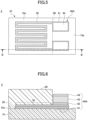
- Fig. 1 is a plan view of an example of a strain gauge according to a first embodiment.
- Fig. 2 is a cross-sectional view of an example of the strain gauge according to the first embodiment, and illustrates a cross section taken along the A-A line in Fig. 1 .
- the strain gauge 1 includes a substrate 10, a functional layer 20, a resistor 30, terminal sections 41, and a cover layer 60. Note that in Fig. 1 , an outer edge of the cover layer 60 is only expressed by a dashed line in order to indicate the resistor 30, for the sake of convenience.
- the side of the substrate 10 where the resistor 30 is provided is referred to as an upper side or one side; and the side of the substrate 10 where the resistor 30 is not provided is referred to as a lower side or another side.
- the surface on the side where the resistor 30 is provided is referred to as one surface or an upper surface; and the surface on the side where the resistor 30 is not provided is referred to as another surface or a lower surface.
- the strain gauge 1 can be used in a state of being upside down, or be disposed at any angle.
- a plan view means that an object is viewed from a normal direction of an upper surface 10a of the substrate 10, and a planar shape refers to a shape of an object when viewed from the normal direction of the upper surface 10a of the substrate 10.
- the substrate 10 is a member that is a base layer for forming the resistor 30 or the like and is flexible.
- the thickness of the substrate 10 is not particularly restricted, and can be appropriately selected for any purpose. For example, such a thickness can be approximately between 5 um and 500 um. In particular, when the thickness of the substrate 10 is between 5 um and 200 um, it is preferable in terms of strain transfer from a flexure element surface that is bonded to a lower surface of the substrate 10 via an adhesive layer or the like; and dimensional stability with respect to environment, and when the thickness is 10 um or more, it is further preferable in terms of insulation.
- the substrate 10 can be formed of an insulating resin film such as a PI (polyimide) resin, an epoxy resin, a PEEK (polyether ether ketone) resin, a PEN (polyethylene naphthalate) resin, a PET (polyethylene terephthalate) resin, a PPS (polyphenylene sulfide) resin, or a polyolefin resin.
- PI polyimide
- PEEK polyether ether ketone
- PEN polyethylene naphthalate
- PET polyethylene terephthalate
- PPS polyphenylene sulfide
- the "formed of an insulating resin film” is not intended to preclude the substrate 10 from containing fillers, impurities, or the like in the insulating resin film.
- the substrate 10 may be formed of, for example, an insulating resin film containing fillers such as silica or alumina.
- the functional layer 20 is formed, as a lower layer of the resistor 30, on the upper surface 10a of the substrate 10.
- a planar shape of the functional layer 20 is approximately the same as the planar shape of the resistor 30 illustrated in Fig. 1 .
- the thickness of the functional layer 20 can be approximately between 1 nm and 100 nm, for example.
- the functional layer refers to a layer that has a function of promoting crystal growth of the resistor 30 that is at least an upper layer.
- the functional layer 20 preferably further has a function of preventing oxidation of the resistor 30 caused by oxygen and moisture included in the substrate 10, as well as a function of improving adhesion between the substrate 10 and the resistor 30.
- the functional layer 20 may further have other functions.
- the insulating resin film that constitutes the substrate 10 contains oxygen and moisture.
- the resistor 30 includes Cr (chromium)
- the material of the functional layer 20 is not particularly restricted as long as it is material having a function of promoting crystal growth of the resistor 30 that is at least an upper layer.
- Such material can be appropriately selected for any purpose, and includes one or more types of metals selected from a group consisting of, for example, Cr (chromium), Ti (titanium), V (vanadium), Nb (niobium), Ta (tantalum), Ni (nickel), Y (yttrium), Zr (zirconium), Hf (hafnium), Si (silicon), C (carbon), Zn (zinc), Cu (copper), Bi (bismuth), Fe (iron), Mo (molybdenum), W (tungsten), Ru (ruthenium), Rh (rhodium), Re (rhenium), Os (osmium), Ir (iridium), Pt (platinum), Pd (palladium), Ag (silver), Au (gold), Co (cobalt), Mn (manganese), and Al (a
- Examples of the above alloy include FeCr, TiAl, FeNi, NiCr, CrCu, and the like.
- Examples of the above compound include TiN, TaN, Si 3 N 4 , TiO 2 , Ta 2 O 5 , SiO 2 , and the like.
- the resistor 30 is a thin film formed in a predetermined pattern and above the upper surface of the functional layer 20, and is a sensitive section where resistance varies according to strain. Note that in Fig. 1 , for the sake of convenience, the resistor 30 is illustrated in a crepe pattern.
- the resistor 30 can be formed of, for example, material including Cr (chromium); material including Ni (nickel); or material including both of Cr and Ni. In other words, the resistor 30 can be formed of material including at least one from among Cr and Ni.
- An example of the material including Cr includes a Cr composite film.
- An example of the material including nickel includes Cu-Ni (copper nickel).
- An example of the material including both of Cr and Ni includes Ni-Cr (nickel chromium).
- the Cr composite film is a composite film of Cr, CrN, Cr 2 N, and the like.
- the Cr composite film may include incidental impurities such as chromium oxide. A portion of the material that constitutes the functional layer 20 may also be diffused into the Cr composite film. In this case, the material that constitutes the functional layer 20, and nitrogen may form a compound.
- the Cr composite film may include Ti or TiN (titanium nitride).
- the thickness of the resistor 30 is not particularly restricted, and can be appropriately selected for any purpose.
- the thickness can be, for example, approximately between 0.05 um and 2 um.
- the resistor 30 With the resistor 30 being formed on the functional layer 20, the resistor 30 can be formed by a stable crystalline phase and thus stability of gauge characteristics (a gauge factor, a gauge factor temperature coefficient TCS, and a temperature coefficient of resistance TCR) can be improved.
- the resistor 30 when the resistor 30 is the Cr composite film, in a case of providing the functional layer 20, the resistor 30 can be formed with ⁇ -Cr (alpha-chromium) as the main component. Because ⁇ -Cr has a stable crystalline phase, the stability of the gauge characteristics can be improved.
- ⁇ -Cr alpha-chromium
- a main component means that a target substance has 50% by weight or more of total substances that constitute the resistor.
- the resistor 30 preferably includes ⁇ -Cr of 80% by weight or more, from the viewpoint of improving the gauge characteristics. Note that ⁇ -Cr is Cr having a bcc structure (body-centered cubic structure).
- the gauge characteristics can be improved.
- the gauge factor of the strain gauge 1 can be 10 or more, as well as the gauge factor temperature coefficient TCS and temperature coefficient of resistance TCR can be each in the range of from -1000 ppm/°C to +1000 ppm/°C.
- the expansion coefficient of the substrate 10 is preferably between 7 ppm/K and 20 ppm/K, from the viewpoint of reducing warp in the substrate 10, where the internal stress of the resistor 30 is assumed to be close to zero.
- the expansion coefficient of the substrate 10 can be adjusted by, for example, selecting the material of the substrate 10, selecting the material of the filler contained in the substrate 10, adjusting the content, and the like.
- pinholes may be generated in the resistor 30. If the number of pinholes generated in the resistor 30 exceeds a predetermined value, the gauge characteristics might deteriorate, or the resistor might not serve as a strain gauge.
- the inventors have recognized that one of causes of a pinhole being generated in the resistor 30 relates to filler protruding from the upper surface 10a of the substrate 10.
- the substrate 10 when the substrate 10 includes a filler, a portion of the filler protrudes from the upper surface 10a of the substrate 10, so that surface unevenness on the upper surface 10a of the substrate 10 increases. As a result, the number of pinholes that are generated in the resistor 30 formed above the upper surface 10a of the substrate 10 increases, which results in deterioration of the gauge characteristics, and the like.
- the inventors have found that, when the thickness of the resistor 30 is 0.05 um or more, in a case where the surface unevenness on the upper surface 10a of the substrate 10 is 15 nm or less, the number of pinholes that are generated in the resistor 30 can be suppressed to maintain the gauge characteristics.
- the surface unevenness on the upper surface 10a of the substrate 10 is preferably 15 nm or less, from the viewpoint of reducing the number of pinholes that are generated in the resistor 30 formed above the upper surface 10a of the substrate 10 to maintain the gauge characteristics.
- the surface unevenness is 15 nm or less, even in a case where the substrate 10 includes fillers, the gauge characteristics do not deteriorate.
- the surface unevenness on the upper surface 10a of the substrate 10 may be 0 nm.
- the surface unevenness on the upper surface 10a of the substrate 10 can be reduced by, for example, heating the substrate 10.
- a method of scraping a protrusion by approximately vertically irradiating the upper surface 10a of the substrate 10 with laser light instead of heating of the substrate 10, a method of scraping a protrusion by approximately vertically irradiating the upper surface 10a of the substrate 10 with laser light; a method of cutting a protrusion by moving a water cutter or the like to be parallel to the upper surface 10a of the substrate 10; a method of polishing the upper surface 10a of the substrate 10 with a grinding wheel; a method of pressing the substrate 10 while heating (heat press); or the like, may be used.
- the surface unevenness means arithmetical mean roughness, and is generally expressed by Ra.
- the surface unevenness can be measured by, for example, three-dimensional optical interferometry.
- the terminal sections 41 respectively extend from both end portions of the resistor 30 and are each wider than the resistor 30 to be in an approximately rectangular shape, in a plan view.
- the terminal sections 41 are a pair of electrodes from which a change in a resistance value of the resistor 30 according to strain is output externally, where, for example, a lead wire for an external connection, or the like is joined.
- the resistor 30 extends zigzagged back and forth from one of the terminal sections 41 to another terminal section 41.
- the upper surface of each terminal section 41 may be coated with a metal allowing for better solderability than the terminal section 41.
- the resistor 30 and the terminal sections 41 are expressed by different numerals. However, the resistor and the terminal sections can be integrally formed of the same material, in the same process.
- the cover layer 60 is an insulating resin layer, which is disposed on and above the upper surface 10a of the substrate 10, such that the resistor 30 is coated and the terminal sections 41 are exposed. With the cover layer 60 being provided, mechanical damage, and the like can be prevented from occurring in the resistor 30. Additionally, with the cover layer 60 being provided, the resistor 30 can be protected against moisture, and the like. Note that the cover layer 60 may be provided to cover the entire portion except for the terminal sections 41.
- the cover layer 60 can be formed of an insulating resin such as a PI resin, an epoxy resin, a PEEK resin, a PEN resin, a PET resin, or a PPS resin, a composite resin (e.g., a silicone resin or a polyolefin resin).
- the cover layer 60 may contain fillers or pigments.
- the thickness of the cover layer 60 is not particularly restricted, and can be appropriately selected for any purpose. For example, the thickness may be approximately between 2 um and 30 um.
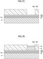
- Figs. 3A to 3C are diagrams illustrating a process of manufacturing the strain gauge according to the first embodiment, and each illustrate a cross section corresponding to Fig. 2 .
- the substrate 10 is prepared and the functional layer 20 is formed on the upper surface 10a of the substrate 10.
- the material and thickness for each of the substrate 10 and the functional layer 20 are the same as the material and thickness described above.
- the functional layer 20 can be vacuum-deposited by, for example, conventional sputtering in which a raw material capable of forming the functional layer 20 is the target and in which an Ar (argon) gas is supplied to a chamber.
- Ar argon
- the functional layer 20 is deposited while the upper surface 10a of the substrate 10 is etched with Ar.
- a deposited amount of film of the functional layer 20 is minimized and thus an effect of improving adhesion can be obtained.
- the functional layer 20 may be formed by other methods.
- the upper surface 10a of the substrate 10 is activated by plasma treatment using Ar, etc. or the like to thereby obtain the effect of improving the adhesion; subsequently, the functional layer 20 may be vacuum-deposited by magnetron sputtering.
- the resistor 30 and the terminal sections 41 are formed on the entire upper surface of the functional layer 20, and then the functional layer 20, the resistor 30, and the terminal sections 41 are each patterned in the planar shape as illustrated in Fig. 1 , by photolithography.
- the material and thickness for each of the resistor 30 and the terminal sections 41 are the same as the material and thickness described above.
- the resistor 30 and the terminal sections 41 can be integrally formed of the same material.
- the resistor 30 and the terminal sections 41 can be deposited by, for example, magnetron sputtering in which a raw material capable of forming the resistor 30 and the terminal sections 41 is a target. Instead of the magnetron sputtering, the resistor 30 and the terminal sections 41 may be deposited by reactive sputtering, vapor deposition, arc ion plating, pulsed laser deposition, or the like.
- a combination of the material of the functional layer 20 and the material of the resistor 30 and the terminal sections 41 is not particularly restricted, and can be appropriately selected for any purpose.
- Ti is used for the functional layer 20, and a Cr composite film formed with ⁇ -Cr (alpha-chromium) as the main component can be deposited as the resistor 30 and the terminal sections 41.
- each of the resistor 30 and the terminal sections 41 can be deposited by, for example, magnetron sputtering in which a raw material capable of forming the Cr composite film is the target and in which an Ar gas is supplied to a chamber.
- the resistor 30 and the terminal sections 41 may be deposited by reactive sputtering in which pure Cr is the target and in which an appropriate amount of nitrogen gas, as well as an Ar gas, are supplied to a chamber.
- a growth face of the Cr composite film is defined by the functional layer 20 formed of Ti, and a Cr composite film that is formed with ⁇ -Cr as the main component having a stable crystalline structure can be deposited. Also, Ti that constitutes the functional layer 20 is diffused into the Cr composite film, so that the gauge characteristics are improved.
- the gauge factor of the strain gauge 1 can be 10 or more, as well as the gauge factor temperature coefficient TCS and temperature coefficient of resistance TCR can be each in the range of from -1000 ppm/° C to +1000 ppm/° C.
- the functional layer 20 formed of Ti includes all functions being a function of promoting crystal growth of the resistor 30; a function of preventing oxidation of the resistor 30 caused by oxygen or moisture contained in the substrate 10; and a function of improving adhesion between the substrate 10 and the resistor 30.
- the functional layer 20 is formed of Ta, Si, Al, or Fe, the functional layer also includes the same functions.
- the cover layer 60 is formed on and above the upper surface 10a of the substrate 10, such that the resistor 30 is coated and the terminal sections 41 are exposed.
- the material and thickness of the cover layer 60 are the same as the material and thickness described above.
- the cover layer 60 can be fabricated, such that a thermosetting insulating resin film in a semi-cured state is laminated on the upper surface 10a of the substrate 10, and such that the resistor 30 is coated and the terminal sections 41 are exposed; subsequently, heat is added and curing is performed.
- the cover layer 60 may be formed, such that a thermosetting insulating resin that is liquid or paste-like is applied to the upper surface 10a of the substrate 10, and such that the resistor 30 is coated and the terminal sections 41 are exposed; subsequently, heat is added and curing is performed. In the above process, the strain gauge 1 is completed.
- the crystal growth of the resistor 30 can be promoted and thus the resistor 30 having a stable crystalline phase can be fabricated.
- the stability of the gauge characteristics can be improved.
- the material that constitutes the functional layer 20 is diffused into the resistor 30, so that the gauge characteristics of the strain gauge 1 can be thereby improved.
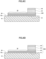
- Modification 1 of the first embodiment provides an example of a strain gauge in which an insulating layer is provided in a lower layer of the cover layer. Note that in the modification 1 of the first embodiment, the explanation for the same components as the embodiment that has been described may be omitted.
- Fig. 4 is a cross-sectional view illustrating an example of the strain gauge according to the modification 1 of the first embodiment, and illustrates a cross section corresponding to Fig. 2 .
- the strain gauge 1A differs from the strain gauge 1 (see Figs. 1 and 2 , etc.) in that an insulating layer 50 is provided in the lower layer of the cover layer 60.
- the cover layer 60 may be provided to cover all portions except for the terminal sections 41.
- the insulating layer 50 is provided on and above the upper surface 10a of the substrate 10, such that the resistor 30 is coated and the terminal sections 41 are exposed.
- the cover layer 60 can be provided to cover a portion of a side surface of the insulating layer 50, and an upper surface thereof.
- the material of the insulating layer 50 is not particularly restricted as long as the material has higher resistance than the resistor 30 and the cover layer 60.
- the material can be appropriately selected for any purpose.
- an oxide or a nitride, such as Si, W, Ti, or Ta, can be used.
- the thickness of the insulating layer 50 is not particularly restricted, and can be appropriately selected for any purpose. For example, the thickness can be approximately between 0.05 um and 1 ⁇ m.
- the method of forming the insulating layer 50 is not particularly restricted, and can be appropriately selected for any purpose.
- a vacuum process such as sputtering or chemical vapor deposition (CVD), or, a solution process such as spin coating or a sol-gel process can be used.
- the insulating layer 50 being provided in the lower layer of the cover layer 60, insulation and environmental sealing can be improved in comparison to the case where the cover layer 60 alone is used. In such a manner, the insulating layer 50 can be appropriately provided according to a specification required for the insulation and environmental sealing.
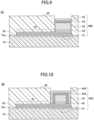
- the second embodiment provides an example of a strain gauge in which each electrode has a laminated structure. Note that in the second embodiment, the explanation for the same components as the embodiment that has been described may be omitted.
- Fig. 5 is a plan view illustrating an example of a strain gauge according to the second embodiment.
- Fig. 6 is a cross-sectional view illustrating an example of the strain gauge according to the second embodiment, and illustrates a cross section taken along the line B-B in Fig. 5 .
- the strain gauge 2 includes electrodes 40A in each of which a plurality of layers are laminated. Note that the cover layer 60 may be provided to cover all portions except for the electrodes 40A.
- Each electrode 40A has a laminated structure in which a plurality of metallic layers are laminated. Specifically, each electrode 40A includes a terminal section 41 extending from a corresponding end portion from among both end portions of the resistor 30; a metallic layer 42 formed on an upper surface of the terminal section 41; a metallic layer 43 formed on an upper surface of the metallic layer 42; and a metallic layer 44 formed on an upper surface of the metallic layer 43.
- the metallic layer 43 is a typical example of a first metallic layer according to the present invention
- the metallic layer 44 is a typical example of a second metallic layer according to the present invention.
- the material of the metallic layer 42 is not particularly restricted, and can be appropriately selected for any purpose.
- Cu copper
- the thickness of the metallic layer 42 is not particularly restricted, and can be appropriately selected for any purpose.
- the thickness can be approximately in the range of from 0.01 um to 1 ⁇ m.
- the material of the metallic layer 43 includes Cu, a Cu alloy, Ni, or a Ni alloy.
- the thickness of the metallic layer 43 is determined in consideration of solderability to the electrode 40A, and is preferably 1 um or more, and more preferably 3 um or more.
- the material of the metallic layer 43 includes Cu, a Cu alloy, Ni, or a Ni alloy and the thickness of the metallic layer 43 is 1 um or more, dissolution of metallization is ameliorated.
- the material of the metallic layer 43 includes Cu, a Cu alloy, Ni, or a Ni alloy and the thickness of the metallic layer 43 is 3 um or more, dissolution of metallization is further ameliorated.
- the thickness of the metallic layer 43 is preferably 30 um or less in terms of ease of electrolytic plating.
- the dissolution of metallization means that the material constituting the electrode 40A is dissolved in solder for jointing the electrode 40A, and that the thickness of the electrode 40A is reduced or the material disappears.
- adhesion strength or tensile strength with a lead wire, or the like to be jointed to the electrode 40A may be reduced.
- the material of the metallic layer 44 material having better solder wettability than the metallic layer 43 can be selected.
- the material of the metallic layer 44 can include Au (gold).
- Au gold
- the surface of Cu, a Cu alloy, Ni, or a Ni alloy is coated with Au, oxidation and corrosion for Cu, a Cu alloy, Ni, or a Ni alloy can be prevented, as well as good solder wettability can be provided.
- Pt platinum
- the metallic layer 44 has the same effect.
- the thickness of the metallic layer 44 is not particularly restricted, and can be appropriately selected for any purpose. For example, the thickness can be approximately between 0.01 ⁇ m and 1 um.
- each terminal section 41 is exposed around a given laminated section of the metallic layers 42, 43, and 44, in a plan view.
- each terminal section 41 may have the same planar shape as the laminated section of the metallic layers 42, 43, and 44.
- Figs. 7A to 8D illustrate a process of manufacturing a strain gauge according to a second embodiment, and illustrate a cross section corresponding to Fig. 6 .
- a process that is similar to that in Fig. 3A according to the first embodiment is first performed, and then in the process illustrated in Fig. 7A , a metallic layer 300 is formed on an upper surface of the functional layer 20.
- the metallic layer 300 is a layer that is finally patterned to serve as the resistor 30 and terminal sections 41.
- the material and thickness of the metallic layer 300 are the same as the material and thickness for each of the above resistor 30 and terminal sections 41.
- the metallic layer 300 can be deposited by magnetron sputtering in which, for example, a raw material capable of forming the metallic layer 300 is the target. Instead of the magnetron sputtering, the metallic layer 300 may be deposited by reactive sputtering, vapor deposition, arc ion plating, pulsed laser deposition, or the like.
- a seed layer 420 as the metallic layer 42 is formed by, for example, sputtering, electroless plating, or the like, to cover an upper surface of the metallic layer 300.
- a photosensitive resist 800 is formed on the entire upper surface of the seed layer 420, and by exposing and developing, an opening 800x for exposing a region in which each electrode 40A is to be formed is formed.
- the resist 800 for example, a dry film resist, or the like can be used.
- a given metallic layer 43 is formed on the seed layer 420 that is exposed in the opening 800x, by for example, electrolytic plating in which the seed layer 420 is set as a power supply path, and further, a given metallic layer 44 is formed on the metallic layer 43.
- the electrolytic plating is suitable because it has high takt and allows for formation of a low stress electrolytic plating layer as the metallic layer 43.
- the metallic layer 44 may be formed on the metallic layer 43, by electroless plating.
- the resist 800 illustrated in Fig. 7D is removed.
- the resist 800 can be removed by, for example, immersing the material of the resist 800 in a dissolvable solution.
- a photosensitive resist 810 is formed on the entire upper surface of the seed layer 420, and by exposing and developing, a planar shape that is the same as that of the resistor 30 and terminal sections 41 in Fig. 5 is patterned.
- the resist 810 for example, a dry film resist, or the like can be used.
- the resist 810 is used as an etch mask, and the functional layer 20, the metallic layer 300, and the seed layer 420 that are exposed from the resist 810 are removed, so that the functional layer 20, the resistor 30, and the terminal sections 41 each of which has the planar shape in Fig. 5 are formed.
- the functional layer 20; the metallic layer 300; and the seed layer 420 can be removed. Note that at this point, the seed layer 420 is formed on the resistor 30.
- the metallic layer 43 and the metallic layer 44 are used as etch masks, and an unwanted seed layer 420 that is exposed from the metallic layer 43 and the metallic layer 44 is removed, so that the metallic layer 42 is formed.
- the unwanted seed layer 420 can be removed.
- the cover layer 60 with which the resistor 30 is coated and that exposes the electrodes 40A is formed on and above the upper surface 10a of the substrate 10, so that the strain gauge 2 is completed.
- each electrode 40A As described above, as each electrode 40A, a given metallic layer 43 formed of a thick film (1 um or more), which is formed of Cu, a Cu alloy, Ni, or a Ni alloy, is formed above a given terminal section 41, and further, a given metallic layer 44 formed of material (Au or Pt) that has better solder wettability than the metallic layer 43 is formed in the outermost surface layer. Thereby, dissolution of metallization can be prevented, as well as improving solder wettability.
- Modification 1 of the second embodiment provides an example of electrodes each having a layer structure different from that in the second embodiment. Note that in the modification 1 of the second embodiment, the explanation for the same components as the embodiments that have been described may be omitted.
- Fig. 9 is a cross-sectional view illustrating an example of a strain gauge according to the modification 1 of the second embodiment, and illustrates a cross section corresponding to Fig. 6 .
- the strain gauge 2A differs from the strain gauge 2 (see Fig. 6 , etc.) in that the electrodes 40A are replaced with electrodes 40B.
- the cover layer 60 is provided to approximately cover all portions except for the electrodes 40B, which differs from the strain gauge 2 (see Fig. 6 , etc.).
- Each electrode 40B has a laminated structure in which a plurality of metallic layers are laminated.
- each electrode 40B includes a terminal section 41 extending from a corresponding end portion from among both end portions of the resistor 30; a metallic layer 42 formed on an upper surface of the terminal section 41; a metallic layer 43 formed on an upper surface of the metallic layer 42; a metallic layer 45 formed on an upper surface of the metallic layer 43; and a metallic layer 44 formed on an upper surface of the metallic layer 45.
- each electrode 40B has a structure in which the metallic layer 45 is provided between the metallic layer 43 and the metallic layer 44 of a given electrode 40A.
- the material of the metallic layer 45 is not particularly restricted, and can be appropriately selected for any purpose.
- Ni can be used.
- NiP nickel phosphorus
- Pd nickel phosphorus
- the metallic layer 45 Ni/Pd (a metallic layer in which a Ni layer and a Pd layer are laminated in this order) may be used.
- the thickness of the metallic layer 45 is not particularly restricted, and can be appropriately selected for any purpose. For example, the thickness is approximately between 1 ⁇ m and 2 um.
- the metallic layer 45 can be formed on the metallic layer 43 by, for example, electrolytic plating in which the seed layer 420 is set as a power supply path.
- the number of electrode layers is not particularly restricted, and the number of layers may be increased as necessary.
- a given metallic layer 43 formed of a thick film (1 um or more), which is formed of Cu, a Cu alloy, Ni, or a Ni alloy, is formed above a given terminal section 41, and further, a given metallic layer 44 formed of material (Au or Pt) that has better solder wettability than the metallic layer 43 is formed in the outermost surface layer.
- Modification 2 of the second embodiment provides another example of electrodes each having a different layer structure from that in the second embodiment. Note that in the modification 2 of the second embodiment, the explanation for the same components as the embodiments that have been described may be omitted.
- Fig. 10 is a cross-sectional view illustrating an example of a strain gauge according to the modification 2 of the second embodiment, and illustrates a cross section corresponding to Fig. 6 .
- the strain gauge 2B differs from the strain gauge 2A (see Fig. 9 ) in that the electrodes 40B are replaced with electrodes 40C.
- the cover layer 60 is provided to approximately cover all portions except for the electrodes 40C, which differs from the strain gauge 2 (see Fig. 6 , etc.).
- Each electrode 40C has a laminated structure in which a plurality of metallic layers are laminated.
- each electrode 40C includes a terminal section 41 extending from a corresponding end portion from among both end portions of the resistor 30; a metallic layer 42 formed on an upper surface of the terminal section 41; a metallic layer 43 formed on an upper surface of the metallic layer 42; a metallic layer 45A formed on an upper surface and side surfaces of the metallic layer 43 and on side surfaces of the metallic layer 42; and a metallic layer 44A formed on an upper surface and side surfaces of the metallic layer 45A.
- the material and thickness for each of the metallic layers 44A and 45A can be the same as the material and thickness of the metallic layers 44 and 45.
- the metallic layer 44A is a typical example of a second metallic layer according to the present invention.
- each electrode 40C In order to form each electrode 40C, first, in the process illustrated in Fig. 7D , for example, a given metallic layer 43 is formed by, for example, electrolytic plating in which the seed layer 420 is set as a power supply path, and then the resist 800 is removed as is the case with the process illustrated in Fig. 8A , without forming a given metallic layer 44. Next, the same process as that in Figs. 8B to 8D is performed. Subsequently, a given metallic layer 45A can be formed on the upper surface and side surfaces of the metallic layer 43 and on the side surfaces of the metallic layer 42, by electroless plating, for example. Additionally, a given metallic layer 44A can be formed on the upper surface and side surfaces of the metallic layer 45A, by electroless plating, for example.
- each electrode can be fabricated by appropriately using both of electrolytic plating and electroless plating.
- a given metallic layer 43 formed of a thick film (1 um or more), which is formed of Cu, a Cu alloy, Ni, or a Ni alloy, is formed above a given terminal section 41, and further, a given metallic layer 44A formed of material (Au or Pt) that has better solder wettability than the metallic layer 43 is formed in the outermost layer.
- the metallic layer 44A of the outermost layer is formed, via the metallic layer 45A, toward the side surfaces of each of the metallic layers 42 and 43, in addition to the upper surface of the metallic layer 43.
- the effect of preventing oxidation and corrosion of Cu, a Cu alloy, Ni, or a Ni alloy that constitutes the metallic layer 43 can be further enhanced, as well as the solder wettability can be further improved.
- the same effect is obtained even when a given metallic layer 44A is formed directly on the upper surface and side surfaces of a given metallic layer 43 and on the side surfaces of a given metallic layer 42, without forming a given metallic layer 45A.
- the metallic layer 44A may directly or indirectly cover the upper surface and side surfaces of the metallic layer 43 and the side surfaces of the metallic layer 42.
- a third embodiment provides an example of a sensor module using a strain gauge. Note that in the third embodiment, the explanation for the same components as the embodiments that have been described may be omitted.
- Fig. 11 is a cross-sectional view illustrating an example of the sensor module according to the third embodiment, and illustrates a cross section corresponding to Fig. 2 .
- the sensor module 5 includes the strain gauge 1, a flexure element 110, and an adhesive layer 120.
- the cover layer 60 may be provided to cover all portions except for the terminal sections 41.
- an upper surface 110a of the flexure element 110 is secured to the lower surface 10b of the substrate 10, via the adhesive layer 120.
- the flexure element 110 is an object that is formed of a metal such as Fe, SUS (stainless steel), or Al, or, a resin such as PEEK, and that is deformed (causes strain) according to force that is applied.
- the strain gauge 1 can detect strain generated in the flexure element 110, as a change in a resistance value of the resistor 30.
- the material of the adhesive layer 120 is not particularly restricted as long as it has a function of securing the flexure element 110 to the strain gauge 1.
- the material can be appropriately selected for any purpose.
- an epoxy resin, a modified epoxy resin, a silicone resin, a modified silicone resin, a urethane resin, a modified urethane resin, or the like can be used.
- material such as a bonding sheet may be used.
- the thickness of the adhesive layer 120 is not particularly restricted, and can be appropriately selected for any purpose. For example, the thickness can be approximately between 0.1 um and 50 um.
- any material described above, which constitutes the adhesive layer 120 is applied to the lower surface 10b of the substrate 10 and/or the upper surface 110a of the flexure element 110. Then, the lower surface 10b of the substrate 10 is situated facing the upper surface 110a of the flexure element 110, and the strain gauge 1 is disposed above the flexure element 110, through the applied material. Alternatively, the bonding sheet may be interposed between the flexure element 110 and the substrate 10.
- the strain gauge 1 is heated to a predetermined temperature while being pressed toward the flexure element 110, and the applied material is cured, so that the adhesive layer 120 is formed.
- the lower surface 10b of the substrate 10 is secured to the upper surface 110a of the flexure element 110, through the adhesive layer 120, so that the sensor module 5 is completed.
- the sensor module 5 can be applied in measurement of load, pressure, torque, acceleration, or the like.
- the strain gauge 1A, 2, 2A, or 2B may be used instead of the strain gauge 1.
- Ti as the functional layer 20 was vacuum-deposited on the upper surface 10a of the substrate 10 formed of a polyimide resin that had a thickness of 25 um, by conventional sputtering.
- five samples for each of which Ti was deposited were fabricated in order to target multiple film thicknesses.
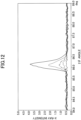
- X-ray fluorescence (XRF) analysis was performed to obtain the result as illustrated in Fig. 12 .
- XRF X-ray fluorescence
- Example 1 Ti as the functional layer 20, which had a film thickness of 3 nm, was vacuum-deposited on the upper surface 10a of the substrate 10 formed of a polyimide resin that had a thickness of 25 ⁇ m, by conventional sputtering.
- a Cr composite film as the resistor 30 and the terminal sections 41, was deposited on the entire upper surface of the functional layer 20, by magnetron sputtering, and then the functional layer 20, the resistor 30, and the terminal sections 41 were patterned by photolithography, as illustrated in Fig. 1 .
- a Cr composite film, as the resistor 30 and the terminal sections 41 was deposited on the upper surface 10a of the substrate 10 formed of a polyimide resin that had a thickness of 25 ⁇ m, by magnetron sputtering. Then, patterning was performed by photolithography, as illustrated in Fig. 1 . Note that for the sample used in Example 1 and the sample used in comparative example 1, all deposition conditions for the resistor 30 and the terminal sections 41 are the same.
- Fig. 13 illustrates an X-ray diffraction pattern at a diffraction angle of 2 ⁇ being in the range of from 36 to 48 degrees, and a diffraction peak in Example 1 is shifted to the right in comparison to a diffraction peak in comparative example 1. Further, the diffraction peak in Example 1 is greater than the diffraction peak in comparative example 1.
- Example 1 The diffraction peak in Example 1 is situated in proximity to a diffraction line of ⁇ -Cr (110). This is considered that when the functional layer 20 formed of Ti was provided, crystal growth of ⁇ -Cr was promoted to thereby form a Cr composite film with ⁇ -Cr as the main component.
- Example 1 multiple samples used in Example 1 and comparative example 1 were fabricated, and gauge characteristics were measured. As a result, a gauge factor for each sample in Example 1 was between 14 and 16. In contrast, a gauge factor for each sample in comparative example 1 was less than 10.
- the gauge factor temperature coefficient TCS and temperature coefficient of resistance TCR were each in the range of from -1000 ppm/° C to +1000 ppm/° C.
- the gauge factor temperature coefficient TCS and temperature coefficient of resistance TCR were not each in the range of from -1000 ppm/° C to +1000 ppm/° C.
- Example 2 multiple substrates 10 each formed of a polyimide resin that had a thickness of 25 um and that had a different expansion coefficient were prepared. Then, when a Cr-composite film, as a given resistor 30, was deposited, a relationship between an expansion coefficient of a given substrate 10 and internal stress of the resistor 30 was checked, to thereby obtain the result illustrated in Fig. 14 .
- the internal stress of the resistor 30 was estimated by measuring warp in an evaluation sample and using the Stoney formula given by Formula (1). Note that as can be seen from Formula (1), the internal stress of the resistor 30 illustrated in Fig. 14 indicates a value per unit thickness and does not depend on the thickness of the resistor 30.
- INTERNAL STRESS ED 2 / 6 1 ⁇ ⁇ tR
- E denotes Young's modulus
- v denotes Poisson's ratio
- D denotes the thickness of the substrate 10
- t denotes the thickness of the resistor 30, and R denotes change in radius of curvature in the substrate 10.
- ⁇ 0.4 GPa indicates values expressing a permittable warp in the strain gauge 1 for functioning, and was experimentally determined by the inventors.
- the expansion coefficient of the substrate 10 is required to be in the range of from 7 ppm/K to 20 ppm/K.
- the material of the substrate 10 does not necessarily include a polyimide resin.
- the expansion coefficient of the substrate 10 can be in the range of from 7 ppm/K to 20 ppm/K, by selecting the material of the substrate 10, selecting the material of the filler contained in the substrate 10, adjusting the content, and the like.
- the expansion coefficient of the substrate 10 being in the range of from 7 ppm/K to 20 ppm/K
- a difference in the expansion coefficient between the substrate 10 and the resistor 30, as well as other factors, are absorbed, so that the internal stress of the resistor 30 can be in the range of ⁇ 0.4 GPa.
- warp in the strain gauge 1 is reduced to thereby cause the strain gauge 1 to be able to function stably in a manner such that good gauge characteristics are maintained.
- Example 3 multiple substrates 10 each formed of a polyimide resin that had a thickness of 25 um and that contained fillers were prepared. Three sets of samples, each of which included a sample not being subject to heat treatment; a sample being subject to heat treatment at a temperature of 100 ° C; a sample being subject to heat treatment at a temperature of 200 ° C; and a sample being subject to heat treatment at a temperature of 300 ° C, were fabricated. Then, the samples were returned to be at normal temperature, and surface unevenness on the upper surface 10a of each substrate 10 was measured by three-dimensional optical interference.
- the resistor 30 having a film thickness of 0.05 um was deposited on the upper surface 10a of each substrate 10, by magnetron sputtering, and patterning was performed by photolithography, as illustrated in Fig. 1 . Then, the number of pinholes that were generated in the resistor 30 was measured by a light transmission method in which light was transmitted from a back surface of a given sample.
- Fig. 15 a relationship between surface unevenness on the upper surface 10a of a given substrate 10 and the number of pinholes that were generated in a given resistor 30 was summarized in Fig. 15 .
- each bar graph illustrated in Fig. 15 shows surface unevenness
- a line graph shows the number of pinholes.
- 100 °C, 200 °C, and 300 °C each indicate a temperature when a given substrate 10 was subject to heat treatment, and Incomplete indicates that heat treatment is not carried out.
- Fig. 15 indicates that when a given substrate 10 is heated at temperatures between 100 °C and 300 °C, the surface unevenness on the upper surface 10a of the substrate 10 is 15 nm or less, which is about half of surface unevenness in a case of being incomplete, and that as a result, the number of pinholes in the resistor 30 is drastically reduced to about 1/7.
- the heat treatment be carried out at temperatures between 100 °C and 250 °C. Note that it is considered that the surface unevenness is reduced by heat treatment because fillers are contained in a polyimide resin that constitutes the substrate 10, during thermal shrinkage caused by the heat treatment.
- the number of pinholes (about 140) in the case of Incomplete, as illustrated in Fig. 15 indicates a level of the gauge characteristics deteriorating.
- the number of pinholes (about 20) after heat treatment indicates a level of the gauge characteristics not being adversely affected.
- the resistor 30 having a film thickness of 0.05 um is used, in a case where the surface unevenness on the upper surface 10a of the substrate 10 is 15 nm or less, it was confirmed that the number of pinholes that were generated in the resistor 30 could be reduced to indicate a level of the gauge characteristics not being adversely affected.
- the resistor 30 having a film thickness of greater than 0.05 um when the resistor 30 having a film thickness of greater than 0.05 um is used, it is obvious that when the surface unevenness on the upper surface 10a of the substrate 10 is 15 nm or less, the number of pinholes that are generated in the resistor 30 can be reduced to indicate a level of the gauge characteristics not being adversely affected. In other words, with the surface unevenness on the upper surface 10a of the substrate 10 being 15 nm or less, when the resistor 30 having a film thickness of 0.05 um or more is used, the number of pinholes that are generated in the resistor 30 can be reduced to indicate a level of the gauge characteristics not being adversely affected.
- the surface unevenness on the upper surface 10a of the substrate 10 can be 15 nm or less, and as a result, the number of pinholes that are generated in the resistor 30 having a film thickness of 0.05 um or more can be significantly reduced. As a result, the strain gauge 1 can function stably in a manner such that good gauge characteristics are maintained.
- the surface unevenness on the upper surface 10a of the substrate 10 can be reduced by, for example, a method of scraping a protrusion by approximately vertically irradiating the upper surface 10a of the substrate 10, with laser light; a method of cutting a protrusion by moving a water cutter or the like to be parallel to the upper surface 10a of the substrate 10; a method of polishing the upper surface 10a of the substrate 10 with a grinding wheel; a method of pressing the substrate 10 while heating (heat press); or the like.
- the surface unevenness on the upper surface 10a of the substrate 10 is not necessarily limited to being directed to surface unevenness caused by the fillers that are present. It is effective to reduce surface unevenness not being caused by the fillers that are present, by various methods described above. For example, when surface unevenness on the substrate 10 without containing fillers is greater than 15 nm, in a case where the surface unevenness on the upper surface 10a of the substrate 10 is 15 nm or less, by various methods described above, the number of pinholes that are generated in the resistor 30 having a film thickness of 0.05 um or more can be reduced to a level of the gauge characteristics not being adversely affected.
- Example 4 the process illustrated in Figs. 7A to 8D was modified as described in the modification 1 of the second embodiment, the strain gauge 2A with the electrodes 40B was fabricated, and the presence or absence of dissolution of metallization was checked. Specifically, 10 types of samples in each of which Cu was used for the metallic layers 42 and 43, in each of which NiP was used for the metallic layer 45, in each of which Au was used for the metallic layer 44, and in each of which the thickness of a given metallic layer was changed were fabricated (samples No. 1 to No. 10), and then the presence or absence of dissolution of metallization was checked.
- Table 1 shows results. Note that in Table 1, the film thickness "0" indicates that no metallic layer was formed. The “poor” indicates that dissolution of metallization occurred in soldering being first performed. The “good” indicates that although no dissolution of metallization occurred in soldering being first performed, little dissolution of metallization occurred in soldering being performed second (where soldering refinement, etc. was assumed). Additionally, the “excellent” indicates that dissolution of metallization occurred neither in soldering being performed first nor second. [Table 1] SAMPLE No.
Landscapes
- Physics & Mathematics (AREA)
- General Physics & Mathematics (AREA)
- Engineering & Computer Science (AREA)
- Microelectronics & Electronic Packaging (AREA)
- Chemical & Material Sciences (AREA)
- Materials Engineering (AREA)
- Mechanical Engineering (AREA)
- Metallurgy (AREA)
- Organic Chemistry (AREA)
- Manufacturing & Machinery (AREA)
- Measurement Of Length, Angles, Or The Like Using Electric Or Magnetic Means (AREA)
Claims (14)
- Dehnungsmesser (1, 1A, 2, 2A, 2B), umfassend:ein flexibles Harzsubstrat (10); undeinen Widerstand (30),wobei der Dehnungsmesser (1, 1A, 2, 2A, 2B) dadurch gekennzeichnet ist, dass er ferner umfasst:eine Funktionsschicht (20), die aus einem Metall, einer Legierung oder einer Metallverbindung direkt auf einer Oberfläche (10a) des Substrats (10) gebildet ist; undeine isolierende Harzschicht (60), mit der der Widerstand (30) beschichtet ist,wobei der Widerstand (30) aus einem Film, der Cr, CrN und Cr2N einschließt, auf einer Oberfläche der Funktionsschicht (20) gebildet ist.
- Dehnungsmesser (1, 1A, 2, 2A, 2B) nach Anspruch 1, wobei der Widerstand (30) aus einem Cr-Verbundfilm gebildet ist, dessen Hauptbestandteil Alpha-Chrom ist, und
die Funktionsschicht (20) eine Funktion einschließt, um das Kristallwachstum des Alpha-Chroms des Widerstands (30) zu fördern. - Dehnungsmesser (1, 1A, 2, 2A, 2B) nach Anspruch 1 oder 2, wobei das Substrat (10) einen Ausdehnungskoeffizienten im Bereich von 7 ppm/K bis 20 ppm/K aufweist.
- Dehnungsmesser (1, 1A, 2, 2A, 2B) nach einem der Ansprüche 1 bis 3, wobei die Oberflächenunebenheit auf der einen Oberfläche (10a) des Substrats (10) 15 nm oder weniger beträgt, und
wobei der Widerstand (30) eine Filmdicke von 0,05 µm oder mehr aufweist. - Dehnungsmesser (2, 2A, 2B) nach einem der Ansprüche 1 bis 4, ferner umfassend Elektroden (40A, 40B, 40C), die elektrisch mit dem Widerstand verbunden sind,
wobei jede Elektrode (40A, 40B, 40C) einschließt:einen Anschlussabschnitt (41), der sich von einem entsprechenden Endabschnitt unter Endabschnitten des Widerstands (30) erstreckt;eine erste Metallschicht (43), die aus Kupfer, einer Kupferlegierung, Nickel oder einer Nickellegierung gebildet ist, auf oder über dem Anschlussabschnitt (41); undeine zweite Metallschicht (44), die aus einem mit Lot benetzbaren Material gebildet ist, das besser benetzbar ist als die erste Metallschicht (43), auf oder über der ersten Metallschicht (43). - Dehnungsmesser (1A) nach einem der Ansprüche 1 bis 5, ferner umfassend eine isolierende Schicht (50), die aus einem Material gebildet ist, das einen höheren Widerstand als der Widerstand (30) und die isolierende Harzschicht (60) aufweist, wobei die isolierende Schicht (50) in einer unteren Schicht der isolierenden Harzschicht (60) bereitgestellt ist und der Widerstand (30) mit der isolierenden Schicht (50) beschichtet ist.
- Dehnungsmesser (1, 1A, 2, 2A, 2B) nach einem der Ansprüche 1 und 3 bis 6, wobei ein Hauptbestandteil des Widerstands (30) Alpha-Chrom ist.
- Dehnungsmesser (1, 1A, 2, 2A, 2B) nach Anspruch 7, wobei der Widerstand (30) 80 Gew.-% Alpha-Chrom oder mehr enthält.
- Dehnungsmesser (1, 1A, 2, 2A, 2B) nach Anspruch 7 oder 8, wobei die Funktionsschicht (20) Titan einschließt.
- Dehnungsmesser (1, 1A, 2, 2A, 2B) nach Anspruch 9, wobei der Widerstand (30) Titan einschließt.
- Dehnungsmesser (1, 1A, 2, 2A, 2B) nach Anspruch 9 oder 10, wobei der Widerstand (30) Titannitrid einschließt.
- Sensormodul (5), umfassend:den Dehnungsmesser (1, 1A, 2, 2A, 2B) nach einem der Ansprüche 1 bis 11; undein Objekt (110), das entsprechend einer ausgeübten Kraft verformt wird, wobei das Objekt (110) auf einer weiteren Oberfläche (10b) des Substrats (10) angeordnet ist.
- Dehnungsmesser (1, 1A, 2, 2A, 2B) nach einem der Ansprüche 1 bis 11, wobei ein in der Funktionsschicht (20) eingeschlossenes Element in einen Cr-Verbundfilm diffundiert ist, dessen Hauptbestandteil Alpha-Chrom des Widerstands (30) ist, das ausgelegt ist, um einen Dehnungsfaktor des Dehnungsmessers (1, 1A, 2, 2A, 2B) von 10 oder mehr zu ermöglichen.
- Dehnungsmesser (1, 1A, 2, 2A, 2B) nach einem der Ansprüche 1 bis 11, wobei ein in der Funktionsschicht (20) eingeschlossenes Element in einen Cr-Verbundfilm diffundiert ist, dessen Hauptbestandteil Alpha-Chrom des Widerstands (30) ist, das ausgelegt ist, um einen Temperaturkoeffizienten des Widerstands des Dehnungsmessers (1, 1A, 2, 2A, 2B) in einem Bereich von -1000 ppm/°C bis +1000 ppm/°C zu ermöglichen.
Applications Claiming Priority (3)
| Application Number | Priority Date | Filing Date | Title |
|---|---|---|---|
| JP2017191824 | 2017-09-29 | ||
| JP2018052422A JP2019066454A (ja) | 2017-09-29 | 2018-03-20 | ひずみゲージ、センサモジュール |
| PCT/JP2018/035727 WO2019065752A1 (ja) | 2017-09-29 | 2018-09-26 | ひずみゲージ、センサモジュール |
Publications (3)
| Publication Number | Publication Date |
|---|---|
| EP3690385A1 EP3690385A1 (de) | 2020-08-05 |
| EP3690385A4 EP3690385A4 (de) | 2021-07-07 |
| EP3690385B1 true EP3690385B1 (de) | 2024-01-17 |
Family
ID=66340597
Family Applications (1)
| Application Number | Title | Priority Date | Filing Date |
|---|---|---|---|
| EP18860610.7A Active EP3690385B1 (de) | 2017-09-29 | 2018-09-26 | Dehnungsmesser und sensormodul |
Country Status (4)
| Country | Link |
|---|---|
| US (1) | US11692806B2 (de) |
| EP (1) | EP3690385B1 (de) |
| JP (1) | JP2019066454A (de) |
| CN (1) | CN111417830B (de) |
Families Citing this family (12)
| Publication number | Priority date | Publication date | Assignee | Title |
|---|---|---|---|---|
| JP2019066453A (ja) | 2017-09-29 | 2019-04-25 | ミネベアミツミ株式会社 | ひずみゲージ |
| JP6793103B2 (ja) | 2017-09-29 | 2020-12-02 | ミネベアミツミ株式会社 | ひずみゲージ |
| JP2019066454A (ja) | 2017-09-29 | 2019-04-25 | ミネベアミツミ株式会社 | ひずみゲージ、センサモジュール |
| JP2019066312A (ja) * | 2017-09-29 | 2019-04-25 | ミネベアミツミ株式会社 | ひずみゲージ |
| JP2019113411A (ja) | 2017-12-22 | 2019-07-11 | ミネベアミツミ株式会社 | ひずみゲージ、センサモジュール |
| JP2019184344A (ja) | 2018-04-05 | 2019-10-24 | ミネベアミツミ株式会社 | ひずみゲージ及びその製造方法 |
| EP3855148A4 (de) | 2018-10-23 | 2022-10-26 | Minebea Mitsumi Inc. | Beschleunigerpedal, lenkvorrichtung , 6-achsen-sensor, motor, stossfänger und dergleichen |
| JP7426794B2 (ja) * | 2019-10-01 | 2024-02-02 | ミネベアミツミ株式会社 | センサモジュール |
| IL275618A (en) * | 2020-06-23 | 2022-01-01 | Vishay Advanced Tech Ltd | Method of manufacture of a strain gage or flexible olyimide-based resistor |
| CN112432720B (zh) * | 2020-11-09 | 2022-08-05 | 浙江工业大学 | 用于潮湿水环境中的载荷传感器元件 |
| JP7189240B2 (ja) * | 2021-01-18 | 2022-12-13 | ミネベアミツミ株式会社 | ひずみゲージ |
| CN115323337B (zh) * | 2022-10-11 | 2023-01-10 | 松诺盟科技有限公司 | 一种纳米薄膜复合应变传感器及其制备方法与应用 |
Citations (1)
| Publication number | Priority date | Publication date | Assignee | Title |
|---|---|---|---|---|
| EP1530708B1 (de) * | 2003-02-19 | 2006-05-17 | Vishay Measurements Group, Inc. | Dehnungsmesser |
Family Cites Families (119)
| Publication number | Priority date | Publication date | Assignee | Title |
|---|---|---|---|---|
| US3867231A (en) | 1972-06-28 | 1975-02-18 | Goodyear Tire & Rubber | Tire building machine |
| JPS5897607A (ja) | 1981-12-07 | 1983-06-10 | Kyowa Dengiyou:Kk | ひずみゲ−ジ |
| JPS58169150A (ja) | 1982-03-30 | 1983-10-05 | Fujitsu Ltd | フオトマスクの製造方法 |
| JPS59164214A (ja) | 1983-03-09 | 1984-09-17 | Nissan Motor Co Ltd | 車両用サスペンシヨン装置 |
| JPS6058578U (ja) | 1983-09-30 | 1985-04-23 | 日産自動車株式会社 | 制動状態検出装置 |
| JPS60104554U (ja) | 1983-12-22 | 1985-07-17 | アルパイン株式会社 | ドアのロツク解除装置 |
| DE3403042A1 (de) | 1984-01-30 | 1985-08-01 | Philips Patentverwaltung Gmbh, 2000 Hamburg | Duennfilm-dehnungsmessstreifen-system und verfahren zu seiner herstellung |
| US4658233A (en) | 1984-03-16 | 1987-04-14 | Fuji Electric Corporate Research & Development Ltd. | Strain gauge |
| DE3429649A1 (de) | 1984-08-11 | 1986-02-20 | Vdo Adolf Schindling Ag, 6000 Frankfurt | Elektrischer widerstand |
| JPS61176803A (ja) * | 1985-01-31 | 1986-08-08 | Hitachi Ltd | ストレインゲージ |
| JPS61288401A (ja) | 1985-06-14 | 1986-12-18 | 株式会社村田製作所 | 薄膜抵抗体 |
| JPS63165725A (ja) * | 1986-12-26 | 1988-07-09 | Aisin Seiki Co Ltd | 圧力センサ−用歪ゲ−ジ |
| US4937550A (en) * | 1987-03-31 | 1990-06-26 | Kanegafuchi Kagaku Kogyo Kabushiki Kaisha | Strain sensor |
| JP2516964B2 (ja) * | 1987-03-31 | 1996-07-24 | 鐘淵化学工業株式会社 | 歪センサ− |
| JPH0731091B2 (ja) | 1987-05-27 | 1995-04-10 | 日本碍子株式会社 | 歪検出器 |
| JP2585681B2 (ja) | 1988-02-08 | 1997-02-26 | 株式会社タイセー | 金属薄膜抵抗ひずみゲ―ジ |
| JPH02117476A (ja) | 1988-10-25 | 1990-05-01 | Daikyo Webasto Co Ltd | 車輌の可動式リヤスポイラー |
| JPH02189981A (ja) | 1989-01-19 | 1990-07-25 | Ricoh Co Ltd | 半導体装置及びその製造法 |
| US5154247A (en) * | 1989-10-31 | 1992-10-13 | Teraoka Seiko Co., Limited | Load cell |
| JPH0495738A (ja) * | 1990-08-06 | 1992-03-27 | Teraoka Seiko Co Ltd | ロードセル |
| JPH03191802A (ja) | 1989-12-21 | 1991-08-21 | Sumitomo Electric Ind Ltd | 感歪素子 |
| JP2890601B2 (ja) | 1990-02-08 | 1999-05-17 | 株式会社デンソー | 半導体センサ |
| DE59102443D1 (de) | 1990-05-07 | 1994-09-08 | Bosch Gmbh Robert | Verfahren zum herstellen eines sensors zum bestimmen von druckkräften. |
| JPH0438402A (ja) * | 1990-06-02 | 1992-02-07 | Kyowa Electron Instr Co Ltd | ひずみゲージとその製造方法 |
| EP0460249B1 (de) | 1990-06-05 | 1994-07-27 | Hottinger Baldwin Messtechnik Gmbh | Dehnungsmessstreifen |
| JPH05308107A (ja) | 1991-07-01 | 1993-11-19 | Sumitomo Electric Ind Ltd | 半導体装置及びその製作方法 |
| JPH0580070A (ja) * | 1991-09-24 | 1993-03-30 | Aisin Seiki Co Ltd | 歪ゲージ素子及びその製造方法 |
| JPH05145142A (ja) | 1991-11-19 | 1993-06-11 | Matsushita Electric Ind Co Ltd | 磁気抵抗素子 |
| JPH0640305A (ja) | 1992-07-23 | 1994-02-15 | Toyota Motor Corp | エアバッグの圧力調整装置 |
| US5328551A (en) | 1992-10-28 | 1994-07-12 | Eaton Corporation | Method of making high output strain gage |
| JPH06176903A (ja) | 1992-12-03 | 1994-06-24 | Nippon Soken Inc | Cr系サーメット薄膜の電極構造 |
| JPH06300649A (ja) * | 1993-04-12 | 1994-10-28 | Sumitomo Electric Ind Ltd | 薄膜歪抵抗材料とその製造方法及び薄膜歪みセンサ |
| JPH07113697A (ja) | 1993-10-19 | 1995-05-02 | Tec Corp | ロードセル |
| JP3233248B2 (ja) * | 1994-05-13 | 2001-11-26 | エヌオーケー株式会社 | 歪ゲ−ジ用薄膜およびその製造法 |
| JPH08102163A (ja) * | 1994-09-30 | 1996-04-16 | Fujitsu Ltd | 磁気記録媒体及び磁気ディスク装置 |
| EP0725392A1 (de) | 1995-01-31 | 1996-08-07 | Hoya Corporation | Magnetisches Aufzeichnungsmedium sowie Verfahren zu seiner Herstellung |
| JPH08304200A (ja) | 1995-05-09 | 1996-11-22 | Matsushita Electric Ind Co Ltd | 感歪み抵抗体ペーストおよびこれを用いた力学量センサ |
| JPH09197435A (ja) | 1996-01-17 | 1997-07-31 | Toshiba Corp | 液晶表示装置、及びその製造方法 |
| JP3642449B2 (ja) | 1997-03-21 | 2005-04-27 | 財団法人電気磁気材料研究所 | Cr−N基歪抵抗膜およびその製造法ならびに歪センサ |
| JP2000146511A (ja) | 1998-11-06 | 2000-05-26 | Mitsubishi Heavy Ind Ltd | 歪ゲージ |
| JP2000207102A (ja) | 1999-01-18 | 2000-07-28 | Alps Electric Co Ltd | キ―ボ―ド装置 |
| WO2001004594A1 (fr) | 1999-07-09 | 2001-01-18 | Nok Corporation | Jauge de contrainte |
| JP2002221453A (ja) * | 2001-01-29 | 2002-08-09 | Nippon Denshi Kogyo Kk | 構造体の荷重情報収集装置 |
| JP4482250B2 (ja) | 2001-07-19 | 2010-06-16 | 本田技研工業株式会社 | 圧力感度及び温度感度を低減したひずみゲージ及びその設計方法 |
| US20030016116A1 (en) | 2001-07-23 | 2003-01-23 | Blaha Charles A. | Method of depositing a thin metallic film and related apparatus |
| JP2003097906A (ja) | 2001-09-27 | 2003-04-03 | Tokyo Sokki Kenkyusho Co Ltd | ひずみゲージ及びひずみ測定方法 |
| JP2003324258A (ja) | 2002-05-01 | 2003-11-14 | Nippon Mektron Ltd | プリント配線板用銅張板 |
| JP2004072715A (ja) | 2002-06-11 | 2004-03-04 | Murata Mfg Co Ltd | 圧電薄膜共振子、圧電フィルタ、およびそれを有する電子部品 |
| CN1300806C (zh) | 2002-06-06 | 2007-02-14 | 阿尔卑斯电气株式会社 | 电阻元件及其制造方法 |
| US7106167B2 (en) | 2002-06-28 | 2006-09-12 | Heetronix | Stable high temperature sensor system with tungsten on AlN |
| EP2848712B1 (de) * | 2002-08-08 | 2018-05-30 | Kabushiki Kaisha Kobe Seiko Sho (Kobe Steel, Ltd.) | Verfahren zur Herstellung einer Aluminiumoxidbeschichtung aus hauptsächlich Alpha-Typ-Kristallstruktur, Aluminiumoxidbeschichtung aus hauptsächlich Alpha-Typ-Kristallstruktur, Laminatbeschichtung mit der Aluminiumoxidbeschichtung, mit der Aluminiumoxidbeschichtung oder der Laminatbeschichtung verkleidetes Element, Verfahren zur Herstellung des Elements und physikalische Gasphasenabscheidungsvorrichtung |
| JP2005132216A (ja) | 2003-10-30 | 2005-05-26 | Matsushita Electric Ind Co Ltd | 踏力センサとそれを用いたペダル踏力検出装置 |
| DE502004010000D1 (de) | 2004-01-27 | 2009-10-15 | Mettler Toledo Ag | Kraftmesszelle mit Dehnmessstreifen mit Klebeschicht aus anorganisch-organischem Hybrid-Polymer (ORMOCER) |
| JP2005233953A (ja) * | 2004-02-17 | 2005-09-02 | Robert Bosch Gmbh | マイクロメカニカル式の高圧センサを製造するための方法及びマクロメカニカル式の圧力センサ |
| JP2006118982A (ja) | 2004-10-21 | 2006-05-11 | Denso Corp | 車両用前方衝突荷重検出装置 |
| JP4742577B2 (ja) | 2004-12-14 | 2011-08-10 | 日産自動車株式会社 | 圧力センサおよびその製造方法 |
| WO2007029253A2 (en) | 2005-09-06 | 2007-03-15 | Beyond Blades Ltd. | 3-dimensional multi-layered modular computer architecture |
| JP4814594B2 (ja) | 2005-09-14 | 2011-11-16 | 日立オートモティブシステムズ株式会社 | 車載設備の操作装置 |
| JP4909583B2 (ja) | 2005-12-16 | 2012-04-04 | 株式会社昭和測器 | 多軸力ロードセル |
| JP2007173544A (ja) * | 2005-12-22 | 2007-07-05 | Toshiba Corp | X線検出器およびその製造方法 |
| EP2080685B1 (de) | 2008-01-16 | 2011-04-27 | Ford Global Technologies, LLC | Drehmomentsensierung mittels integrierter Dehnungsmessstreifen |
| JP2010070850A (ja) | 2008-08-21 | 2010-04-02 | Mitsubishi Materials Corp | 銅張積層板およびその製造方法並びにプリント配線板およびその製造方法 |
| JP5279426B2 (ja) | 2008-09-19 | 2013-09-04 | ミサワホーム株式会社 | ドアロックシステム |
| JP2011103327A (ja) | 2009-11-10 | 2011-05-26 | Seiko Epson Corp | 圧電素子、圧電アクチュエーター、液体噴射ヘッドおよび液体噴射装置 |
| JP2011240794A (ja) | 2010-05-18 | 2011-12-01 | Takashi Aono | 車両認識音発生装置 |
| JP5813103B2 (ja) | 2010-06-11 | 2015-11-17 | スリーエム イノベイティブ プロパティズ カンパニー | 力測定を用いるタッチ位置センサ |
| US8232026B2 (en) | 2010-10-14 | 2012-07-31 | Ford Global Technologies, Llc | Bipolar plates for electrochemical cells |
| JP2012151338A (ja) | 2011-01-20 | 2012-08-09 | Elpida Memory Inc | 半導体装置の製造方法及びハードマスクの形成方法 |
| JP5884110B2 (ja) | 2011-12-02 | 2016-03-15 | 株式会社アサヒ電子研究所 | 歪抵抗素子およびそれを用いた歪検出装置 |
| TWI476969B (zh) | 2012-01-13 | 2015-03-11 | Univ Nat Kaohsiung Applied Sci | Metal silicide thermal sensor and its preparation method |
| JP5539430B2 (ja) | 2012-03-22 | 2014-07-02 | 富士フイルム株式会社 | 電子機器の製造方法 |
| JP2013217763A (ja) | 2012-04-09 | 2013-10-24 | Honda Motor Co Ltd | 薄膜ひずみセンサ用材料およびこれを用いた薄膜ひずみセンサ |
| JP5670502B2 (ja) | 2012-04-30 | 2015-02-18 | 株式会社エスアンドエス テック | 位相反転ブランクマスク及びその製造方法 |
| EP2857816A4 (de) | 2012-05-25 | 2015-12-09 | Hitachi Ltd | Mechanische mengenmessvorrichtung |
| CN103580980B (zh) | 2012-07-24 | 2019-05-24 | 中兴通讯股份有限公司 | 虚拟网络自动发现和自动配置的方法及其装置 |
| JP6022881B2 (ja) * | 2012-10-04 | 2016-11-09 | 公益財団法人電磁材料研究所 | 歪ゲージ |
| US9306207B2 (en) | 2012-12-28 | 2016-04-05 | Hyundai Motor Company | Method of fabricating sulfur-infiltrated mesoporous conductive nanocomposites for cathode of lithium-sulfur secondary battery |
| JP6075114B2 (ja) | 2013-02-27 | 2017-02-08 | ローム株式会社 | 半導体装置および半導体装置の製造方法 |
| WO2015005934A1 (en) | 2013-07-12 | 2015-01-15 | Hewlett-Packard Development Company, L.P. | Thermal inkjet printhead stack with amorphous metal resistor |
| JP6159613B2 (ja) * | 2013-08-05 | 2017-07-05 | 公益財団法人電磁材料研究所 | 歪センサ |
| US20150296607A1 (en) | 2014-04-11 | 2015-10-15 | Apple Inc. | Electronic Device With Flexible Printed Circuit Strain Gauge Sensor |
| CN106461484B (zh) | 2014-06-09 | 2019-04-12 | 日立汽车系统株式会社 | 力学量测量装置及使用其的压力传感器 |
| JP6276658B2 (ja) | 2014-07-09 | 2018-02-07 | 新光電気工業株式会社 | 膜厚測定機能付き基板及び絶縁層の膜厚測定方法 |
| JP6162670B2 (ja) | 2014-10-03 | 2017-07-12 | 株式会社東京測器研究所 | ひずみゲージ用合金及びひずみゲージ |
| US10663357B2 (en) | 2014-12-10 | 2020-05-26 | Paul D OKULOV | Micro electro-mechanical strain displacement sensor and usage monitoring system |
| JP6256360B2 (ja) * | 2015-01-23 | 2018-01-10 | 株式会社豊田中央研究所 | 永久磁石およびその製造方法 |
| JP6411916B2 (ja) | 2015-02-26 | 2018-10-24 | ラピスセミコンダクタ株式会社 | 半導体装置、ワイパシステム、及び移動体制御方法 |
| US9714876B2 (en) | 2015-03-26 | 2017-07-25 | Sensata Technologies, Inc. | Semiconductor strain gauge |
| US9933321B2 (en) | 2015-05-14 | 2018-04-03 | Vishay Measurements Group, Inc. | High gage factor strain gage |
| JP6332303B2 (ja) | 2015-06-01 | 2018-05-30 | 日亜化学工業株式会社 | 金属被覆方法及び発光装置とその製造方法 |
| DE112016002769T5 (de) | 2015-06-19 | 2018-03-29 | Semiconductor Energy Laboratory Co., Ltd. | Halbleitervorrichtung, Herstellungsverfahren dafür und elektronisches Gerät |
| JP2017067764A (ja) | 2015-09-29 | 2017-04-06 | ミネベアミツミ株式会社 | ひずみゲージ、荷重センサ、及びひずみゲージの製造方法 |
| US10353503B2 (en) | 2015-10-29 | 2019-07-16 | Texas Instruments Incorporated | Integrated force sensing element |
| JP2017101983A (ja) | 2015-12-01 | 2017-06-08 | 日本写真印刷株式会社 | 多点計測用のひずみセンサとその製造方法 |
| JP6701748B2 (ja) | 2016-01-19 | 2020-05-27 | ヤマハ株式会社 | 歪みセンサ素子 |
| US10054503B2 (en) | 2016-03-11 | 2018-08-21 | Microsoft Technology Licensing, Llc | Force sensor |
| CN105755438B (zh) | 2016-03-30 | 2018-12-18 | 上海交通大学 | 一种高温自补偿多层复合薄膜应变计及其制备方法 |
| JP5988004B1 (ja) * | 2016-04-12 | 2016-09-07 | Tdk株式会社 | 電子回路パッケージ |
| JP6607820B2 (ja) * | 2016-04-12 | 2019-11-20 | 東京エレクトロン株式会社 | フィルタ立ち上げ装置、処理液供給装置、治具ユニット、フィルタの立ち上げ方法 |
| DE102016108985A1 (de) | 2016-05-13 | 2017-11-16 | Trafag Ag | Verfahren zur Herstellung eines Sensorelements mittels Laserstrukturierung |
| TWI581170B (zh) | 2016-05-19 | 2017-05-01 | 速博思股份有限公司 | 具金屬走線的壓力觸控裝置 |
| JP2017210572A (ja) | 2016-05-27 | 2017-11-30 | 株式会社ファンケル | 抗酸化組成物 |
| JP7223489B2 (ja) | 2016-05-27 | 2023-02-16 | デンカ株式会社 | 組成物 |
| JP2018048894A (ja) | 2016-09-21 | 2018-03-29 | 株式会社東芝 | センサ及び電子機器 |
| JP2018058549A (ja) | 2016-10-07 | 2018-04-12 | スズキ株式会社 | 車両用盗難防止装置 |
| CN106768524A (zh) * | 2017-02-20 | 2017-05-31 | 广东海洋大学 | 一种薄膜压力传感器及其制造方法 |
| JP6762896B2 (ja) | 2017-03-22 | 2020-09-30 | アズビル株式会社 | 圧力センサチップ、圧力発信器、および圧力センサチップの製造方法 |
| JP2019066453A (ja) * | 2017-09-29 | 2019-04-25 | ミネベアミツミ株式会社 | ひずみゲージ |
| JP2019066454A (ja) | 2017-09-29 | 2019-04-25 | ミネベアミツミ株式会社 | ひずみゲージ、センサモジュール |
| JP2019066313A (ja) | 2017-09-29 | 2019-04-25 | ミネベアミツミ株式会社 | ひずみゲージ |
| JP2019066312A (ja) | 2017-09-29 | 2019-04-25 | ミネベアミツミ株式会社 | ひずみゲージ |
| JP2019082424A (ja) | 2017-10-31 | 2019-05-30 | ミネベアミツミ株式会社 | ひずみゲージ |
| JP2019090723A (ja) | 2017-11-15 | 2019-06-13 | ミネベアミツミ株式会社 | ひずみゲージ |
| JP2019113411A (ja) | 2017-12-22 | 2019-07-11 | ミネベアミツミ株式会社 | ひずみゲージ、センサモジュール |
| JP2019132790A (ja) | 2018-02-02 | 2019-08-08 | ミネベアミツミ株式会社 | ひずみゲージ |
| JP2018132531A (ja) | 2018-05-17 | 2018-08-23 | ミネベアミツミ株式会社 | ひずみゲージ |
| JP6660425B2 (ja) | 2018-07-20 | 2020-03-11 | ミネベアミツミ株式会社 | 姿勢制御装置 |
| JP7193262B2 (ja) | 2018-07-23 | 2022-12-20 | ミネベアミツミ株式会社 | 触覚センサ |
| US20200076016A1 (en) | 2018-09-04 | 2020-03-05 | Hutchinson Technology Incorporated | Sensored Battery Pouch |
-
2018
- 2018-03-20 JP JP2018052422A patent/JP2019066454A/ja active Pending
- 2018-09-26 CN CN201880076801.2A patent/CN111417830B/zh active Active
- 2018-09-26 US US16/650,553 patent/US11692806B2/en active Active
- 2018-09-26 EP EP18860610.7A patent/EP3690385B1/de active Active
Patent Citations (1)
| Publication number | Priority date | Publication date | Assignee | Title |
|---|---|---|---|---|
| EP1530708B1 (de) * | 2003-02-19 | 2006-05-17 | Vishay Measurements Group, Inc. | Dehnungsmesser |
Also Published As
| Publication number | Publication date |
|---|---|
| US11692806B2 (en) | 2023-07-04 |
| EP3690385A4 (de) | 2021-07-07 |
| CN111417830B (zh) | 2023-04-18 |
| JP2019066454A (ja) | 2019-04-25 |
| CN111417830A (zh) | 2020-07-14 |
| EP3690385A1 (de) | 2020-08-05 |
| US20200292294A1 (en) | 2020-09-17 |
Similar Documents
| Publication | Publication Date | Title |
|---|---|---|
| EP3690385B1 (de) | Dehnungsmesser und sensormodul | |
| US11543309B2 (en) | Strain gauge and sensor module | |
| US11543308B2 (en) | Strain gauge | |
| EP3690387B1 (de) | Dehnungsmesser | |
| EP3690388B1 (de) | Dehnungsmesser | |
| EP3690386B1 (de) | Dehnungsmesser | |
| US11499877B2 (en) | Strain gauge | |
| US11448560B2 (en) | Strain gauge and sensor module | |
| US11300398B2 (en) | Strain gauge with improved distortion of measured object | |
| US10921110B2 (en) | Strain gauge | |
| JP2023107860A (ja) | ひずみゲージ、センサモジュール | |
| US11796404B2 (en) | Strain gauge | |
| JP2022093237A (ja) | ひずみゲージ | |
| CN115398178A (zh) | 应变仪 | |
| JP2022075113A (ja) | ひずみゲージ | |
| WO2019098072A1 (ja) | ひずみゲージ | |
| JP2022071494A (ja) | ひずみゲージ | |
| JP2022008026A (ja) | ひずみゲージ |
Legal Events
| Date | Code | Title | Description |
|---|---|---|---|
| STAA | Information on the status of an ep patent application or granted ep patent |
Free format text: STATUS: THE INTERNATIONAL PUBLICATION HAS BEEN MADE |
|
| PUAI | Public reference made under article 153(3) epc to a published international application that has entered the european phase |
Free format text: ORIGINAL CODE: 0009012 |
|
| STAA | Information on the status of an ep patent application or granted ep patent |
Free format text: STATUS: REQUEST FOR EXAMINATION WAS MADE |
|
| 17P | Request for examination filed |
Effective date: 20200427 |
|
| AK | Designated contracting states |
Kind code of ref document: A1 Designated state(s): AL AT BE BG CH CY CZ DE DK EE ES FI FR GB GR HR HU IE IS IT LI LT LU LV MC MK MT NL NO PL PT RO RS SE SI SK SM TR |
|
| AX | Request for extension of the european patent |
Extension state: BA ME |
|
| DAV | Request for validation of the european patent (deleted) | ||
| DAX | Request for extension of the european patent (deleted) | ||
| A4 | Supplementary search report drawn up and despatched |
Effective date: 20210604 |
|
| RIC1 | Information provided on ipc code assigned before grant |
Ipc: G01B 7/16 20060101AFI20210528BHEP Ipc: G01L 1/22 20060101ALI20210528BHEP Ipc: H01C 1/14 20060101ALI20210528BHEP Ipc: H01L 41/12 20060101ALI20210528BHEP Ipc: H01C 3/12 20060101ALI20210528BHEP Ipc: H01C 17/065 20060101ALI20210528BHEP |
|
| RIC1 | Information provided on ipc code assigned before grant |
Ipc: H01C 17/065 20060101ALI20230824BHEP Ipc: H01C 3/12 20060101ALI20230824BHEP Ipc: H01C 1/14 20060101ALI20230824BHEP Ipc: G01L 1/22 20060101ALI20230824BHEP Ipc: G01B 7/16 20060101AFI20230824BHEP |
|
| GRAP | Despatch of communication of intention to grant a patent |
Free format text: ORIGINAL CODE: EPIDOSNIGR1 |
|
| STAA | Information on the status of an ep patent application or granted ep patent |
Free format text: STATUS: GRANT OF PATENT IS INTENDED |
|
| INTG | Intention to grant announced |
Effective date: 20231030 |
|
| GRAS | Grant fee paid |
Free format text: ORIGINAL CODE: EPIDOSNIGR3 |
|
| GRAA | (expected) grant |
Free format text: ORIGINAL CODE: 0009210 |
|
| STAA | Information on the status of an ep patent application or granted ep patent |
Free format text: STATUS: THE PATENT HAS BEEN GRANTED |
|
| AK | Designated contracting states |
Kind code of ref document: B1 Designated state(s): AL AT BE BG CH CY CZ DE DK EE ES FI FR GB GR HR HU IE IS IT LI LT LU LV MC MK MT NL NO PL PT RO RS SE SI SK SM TR |
|
| REG | Reference to a national code |
Ref country code: GB Ref legal event code: FG4D |
|
| REG | Reference to a national code |
Ref country code: DE Ref legal event code: R096 Ref document number: 602018064344 Country of ref document: DE |
|
| REG | Reference to a national code |
Ref country code: CH Ref legal event code: EP |
|
| REG | Reference to a national code |
Ref country code: IE Ref legal event code: FG4D |
|
| REG | Reference to a national code |
Ref country code: LT Ref legal event code: MG9D |