EP3570374B1 - Integrated rf front end - Google Patents
Integrated rf front end Download PDFInfo
- Publication number
- EP3570374B1 EP3570374B1 EP19159039.7A EP19159039A EP3570374B1 EP 3570374 B1 EP3570374 B1 EP 3570374B1 EP 19159039 A EP19159039 A EP 19159039A EP 3570374 B1 EP3570374 B1 EP 3570374B1
- Authority
- EP
- European Patent Office
- Prior art keywords
- circuit
- mosfet
- voltage
- output
- transistor
- Prior art date
- Legal status (The legal status is an assumption and is not a legal conclusion. Google has not performed a legal analysis and makes no representation as to the accuracy of the status listed.)
- Active
Links
- 239000003990 capacitor Substances 0.000 claims description 47
- 238000000034 method Methods 0.000 claims description 41
- 238000010168 coupling process Methods 0.000 claims description 40
- 238000005859 coupling reaction Methods 0.000 claims description 40
- 230000008878 coupling Effects 0.000 claims description 39
- 238000001914 filtration Methods 0.000 claims description 20
- 230000001939 inductive effect Effects 0.000 claims description 5
- 238000010586 diagram Methods 0.000 description 22
- 238000004519 manufacturing process Methods 0.000 description 21
- 230000005540 biological transmission Effects 0.000 description 18
- 239000008186 active pharmaceutical agent Substances 0.000 description 13
- 239000010754 BS 2869 Class F Substances 0.000 description 8
- 230000008901 benefit Effects 0.000 description 8
- 238000013461 design Methods 0.000 description 8
- 230000010354 integration Effects 0.000 description 8
- 230000015556 catabolic process Effects 0.000 description 7
- 230000008569 process Effects 0.000 description 7
- 238000004891 communication Methods 0.000 description 6
- 238000012545 processing Methods 0.000 description 5
- 230000009467 reduction Effects 0.000 description 5
- 230000001413 cellular effect Effects 0.000 description 4
- 230000007423 decrease Effects 0.000 description 4
- 230000000694 effects Effects 0.000 description 4
- 230000001965 increasing effect Effects 0.000 description 4
- 230000003071 parasitic effect Effects 0.000 description 4
- 239000000047 product Substances 0.000 description 4
- 230000003750 conditioning effect Effects 0.000 description 3
- 230000004044 response Effects 0.000 description 3
- 230000003321 amplification Effects 0.000 description 2
- 238000013459 approach Methods 0.000 description 2
- 238000004364 calculation method Methods 0.000 description 2
- 230000001419 dependent effect Effects 0.000 description 2
- 238000005516 engineering process Methods 0.000 description 2
- 230000006872 improvement Effects 0.000 description 2
- 239000002184 metal Substances 0.000 description 2
- 238000003199 nucleic acid amplification method Methods 0.000 description 2
- 230000010355 oscillation Effects 0.000 description 2
- 229910052594 sapphire Inorganic materials 0.000 description 2
- 239000010980 sapphire Substances 0.000 description 2
- 239000004065 semiconductor Substances 0.000 description 2
- 229910052710 silicon Inorganic materials 0.000 description 2
- 239000010703 silicon Substances 0.000 description 2
- 230000000903 blocking effect Effects 0.000 description 1
- 230000008859 change Effects 0.000 description 1
- 230000000295 complement effect Effects 0.000 description 1
- 230000006835 compression Effects 0.000 description 1
- 238000007906 compression Methods 0.000 description 1
- 230000001143 conditioned effect Effects 0.000 description 1
- 238000007596 consolidation process Methods 0.000 description 1
- 239000000470 constituent Substances 0.000 description 1
- 230000003247 decreasing effect Effects 0.000 description 1
- 230000001934 delay Effects 0.000 description 1
- 238000011161 development Methods 0.000 description 1
- FOCAHLGSDWHSAH-UHFFFAOYSA-N difluoromethanethione Chemical compound FC(F)=S FOCAHLGSDWHSAH-UHFFFAOYSA-N 0.000 description 1
- 230000009977 dual effect Effects 0.000 description 1
- 230000002708 enhancing effect Effects 0.000 description 1
- 230000005669 field effect Effects 0.000 description 1
- 239000012467 final product Substances 0.000 description 1
- 239000012212 insulator Substances 0.000 description 1
- 238000002955 isolation Methods 0.000 description 1
- 210000003127 knee Anatomy 0.000 description 1
- 230000000737 periodic effect Effects 0.000 description 1
- 238000006467 substitution reaction Methods 0.000 description 1
- 230000002459 sustained effect Effects 0.000 description 1
Images


Classifications
-
- H—ELECTRICITY
- H04—ELECTRIC COMMUNICATION TECHNIQUE
- H04B—TRANSMISSION
- H04B1/00—Details of transmission systems, not covered by a single one of groups H04B3/00 - H04B13/00; Details of transmission systems not characterised by the medium used for transmission
- H04B1/38—Transceivers, i.e. devices in which transmitter and receiver form a structural unit and in which at least one part is used for functions of transmitting and receiving
- H04B1/40—Circuits
- H04B1/44—Transmit/receive switching
- H04B1/48—Transmit/receive switching in circuits for connecting transmitter and receiver to a common transmission path, e.g. by energy of transmitter
-
- H—ELECTRICITY
- H01—ELECTRIC ELEMENTS
- H01L—SEMICONDUCTOR DEVICES NOT COVERED BY CLASS H10
- H01L27/00—Devices consisting of a plurality of semiconductor or other solid-state components formed in or on a common substrate
- H01L27/02—Devices consisting of a plurality of semiconductor or other solid-state components formed in or on a common substrate including semiconductor components specially adapted for rectifying, oscillating, amplifying or switching and having at least one potential-jump barrier or surface barrier; including integrated passive circuit elements with at least one potential-jump barrier or surface barrier
- H01L27/0203—Particular design considerations for integrated circuits
- H01L27/0248—Particular design considerations for integrated circuits for electrical or thermal protection, e.g. electrostatic discharge [ESD] protection
-
- H—ELECTRICITY
- H01—ELECTRIC ELEMENTS
- H01Q—ANTENNAS, i.e. RADIO AERIALS
- H01Q23/00—Antennas with active circuits or circuit elements integrated within them or attached to them
-
- H—ELECTRICITY
- H03—ELECTRONIC CIRCUITRY
- H03F—AMPLIFIERS
- H03F1/00—Details of amplifiers with only discharge tubes, only semiconductor devices or only unspecified devices as amplifying elements
- H03F1/02—Modifications of amplifiers to raise the efficiency, e.g. gliding Class A stages, use of an auxiliary oscillation
- H03F1/0205—Modifications of amplifiers to raise the efficiency, e.g. gliding Class A stages, use of an auxiliary oscillation in transistor amplifiers
-
- H—ELECTRICITY
- H03—ELECTRONIC CIRCUITRY
- H03F—AMPLIFIERS
- H03F1/00—Details of amplifiers with only discharge tubes, only semiconductor devices or only unspecified devices as amplifying elements
- H03F1/08—Modifications of amplifiers to reduce detrimental influences of internal impedances of amplifying elements
- H03F1/22—Modifications of amplifiers to reduce detrimental influences of internal impedances of amplifying elements by use of cascode coupling, i.e. earthed cathode or emitter stage followed by earthed grid or base stage respectively
- H03F1/223—Modifications of amplifiers to reduce detrimental influences of internal impedances of amplifying elements by use of cascode coupling, i.e. earthed cathode or emitter stage followed by earthed grid or base stage respectively with MOSFET's
-
- H—ELECTRICITY
- H03—ELECTRONIC CIRCUITRY
- H03F—AMPLIFIERS
- H03F1/00—Details of amplifiers with only discharge tubes, only semiconductor devices or only unspecified devices as amplifying elements
- H03F1/56—Modifications of input or output impedances, not otherwise provided for
-
- H—ELECTRICITY
- H03—ELECTRONIC CIRCUITRY
- H03F—AMPLIFIERS
- H03F1/00—Details of amplifiers with only discharge tubes, only semiconductor devices or only unspecified devices as amplifying elements
- H03F1/56—Modifications of input or output impedances, not otherwise provided for
- H03F1/565—Modifications of input or output impedances, not otherwise provided for using inductive elements
-
- H—ELECTRICITY
- H03—ELECTRONIC CIRCUITRY
- H03F—AMPLIFIERS
- H03F3/00—Amplifiers with only discharge tubes or only semiconductor devices as amplifying elements
- H03F3/189—High frequency amplifiers, e.g. radio frequency amplifiers
-
- H—ELECTRICITY
- H03—ELECTRONIC CIRCUITRY
- H03F—AMPLIFIERS
- H03F3/00—Amplifiers with only discharge tubes or only semiconductor devices as amplifying elements
- H03F3/189—High frequency amplifiers, e.g. radio frequency amplifiers
- H03F3/19—High frequency amplifiers, e.g. radio frequency amplifiers with semiconductor devices only
-
- H—ELECTRICITY
- H03—ELECTRONIC CIRCUITRY
- H03F—AMPLIFIERS
- H03F3/00—Amplifiers with only discharge tubes or only semiconductor devices as amplifying elements
- H03F3/20—Power amplifiers, e.g. Class B amplifiers, Class C amplifiers
- H03F3/21—Power amplifiers, e.g. Class B amplifiers, Class C amplifiers with semiconductor devices only
- H03F3/217—Class D power amplifiers; Switching amplifiers
- H03F3/2171—Class D power amplifiers; Switching amplifiers with field-effect devices
-
- H—ELECTRICITY
- H03—ELECTRONIC CIRCUITRY
- H03F—AMPLIFIERS
- H03F3/00—Amplifiers with only discharge tubes or only semiconductor devices as amplifying elements
- H03F3/68—Combinations of amplifiers, e.g. multi-channel amplifiers for stereophonics
-
- H—ELECTRICITY
- H03—ELECTRONIC CIRCUITRY
- H03G—CONTROL OF AMPLIFICATION
- H03G11/00—Limiting amplitude; Limiting rate of change of amplitude ; Clipping in general
-
- H—ELECTRICITY
- H03—ELECTRONIC CIRCUITRY
- H03G—CONTROL OF AMPLIFICATION
- H03G3/00—Gain control in amplifiers or frequency changers without distortion of the input signal
- H03G3/20—Automatic control
- H03G3/30—Automatic control in amplifiers having semiconductor devices
- H03G3/3036—Automatic control in amplifiers having semiconductor devices in high-frequency amplifiers or in frequency-changers
- H03G3/3042—Automatic control in amplifiers having semiconductor devices in high-frequency amplifiers or in frequency-changers in modulators, frequency-changers, transmitters or power amplifiers
-
- H—ELECTRICITY
- H04—ELECTRIC COMMUNICATION TECHNIQUE
- H04B—TRANSMISSION
- H04B1/00—Details of transmission systems, not covered by a single one of groups H04B3/00 - H04B13/00; Details of transmission systems not characterised by the medium used for transmission
- H04B1/005—Details of transmission systems, not covered by a single one of groups H04B3/00 - H04B13/00; Details of transmission systems not characterised by the medium used for transmission adapting radio receivers, transmitters andtransceivers for operation on two or more bands, i.e. frequency ranges
- H04B1/0053—Details of transmission systems, not covered by a single one of groups H04B3/00 - H04B13/00; Details of transmission systems not characterised by the medium used for transmission adapting radio receivers, transmitters andtransceivers for operation on two or more bands, i.e. frequency ranges with common antenna for more than one band
-
- H—ELECTRICITY
- H04—ELECTRIC COMMUNICATION TECHNIQUE
- H04B—TRANSMISSION
- H04B1/00—Details of transmission systems, not covered by a single one of groups H04B3/00 - H04B13/00; Details of transmission systems not characterised by the medium used for transmission
- H04B1/02—Transmitters
- H04B1/04—Circuits
- H04B1/0475—Circuits with means for limiting noise, interference or distortion
-
- H—ELECTRICITY
- H04—ELECTRIC COMMUNICATION TECHNIQUE
- H04L—TRANSMISSION OF DIGITAL INFORMATION, e.g. TELEGRAPHIC COMMUNICATION
- H04L27/00—Modulated-carrier systems
- H04L27/02—Amplitude-modulated carrier systems, e.g. using on-off keying; Single sideband or vestigial sideband modulation
- H04L27/04—Modulator circuits; Transmitter circuits
-
- H—ELECTRICITY
- H03—ELECTRONIC CIRCUITRY
- H03F—AMPLIFIERS
- H03F2200/00—Indexing scheme relating to amplifiers
- H03F2200/294—Indexing scheme relating to amplifiers the amplifier being a low noise amplifier [LNA]
-
- H—ELECTRICITY
- H03—ELECTRONIC CIRCUITRY
- H03F—AMPLIFIERS
- H03F2200/00—Indexing scheme relating to amplifiers
- H03F2200/372—Noise reduction and elimination in amplifier
-
- H—ELECTRICITY
- H03—ELECTRONIC CIRCUITRY
- H03F—AMPLIFIERS
- H03F2200/00—Indexing scheme relating to amplifiers
- H03F2200/387—A circuit being added at the output of an amplifier to adapt the output impedance of the amplifier
-
- H—ELECTRICITY
- H03—ELECTRONIC CIRCUITRY
- H03F—AMPLIFIERS
- H03F2200/00—Indexing scheme relating to amplifiers
- H03F2200/451—Indexing scheme relating to amplifiers the amplifier being a radio frequency amplifier
-
- H—ELECTRICITY
- H03—ELECTRONIC CIRCUITRY
- H03F—AMPLIFIERS
- H03F2200/00—Indexing scheme relating to amplifiers
- H03F2200/61—Indexing scheme relating to amplifiers the cascode amplifier has more than one common gate stage
Definitions
- This invention relates broadly to integrated electronic circuits, and more specifically to RF transceiver circuitry.
- Wireless communications devices are undergoing sustained development.
- the extreme popularity of cellular mobile telephones has motivated improvements in efficiency, speed, size and cost-effectiveness for RF transmission circuits in handheld devices. Enhancing the efficiency of such circuits is highly desirable so that the size of the required batteries may be reduced, while their life is extended. Cost-effectiveness is clearly always desirable for consumer products, particularly when such products require periodic replacement to stay abreast of changes in the technology.
- Most wireless communication units such as cellular telephones, comprise at least one RF transceiver.
- a communication device such as a cellular telephone, may comprise a multiplicity of RF (radio frequency) front end circuits, which are of primary interest herein.
- RF front end circuits typically include an RF transmit signal amplifier, a Power Amplifier (PA), a matching and filtering section, an antenna switch, and may include a received signal amplifier.
- PA Power Amplifier
- a complete transceiver generally also includes a low-noise amplifier for the received signal.
- the PA subcircuit is typically the most power-consuming portion of such transmitters, and, also typically, is the source of the most significant unintended or "spurious" emissions.
- PAs of class A, B, C, D, E and F are well known in the art.
- the primary amplifying devices in PAs of classes A-C are designed to operate in an "active" region of their operating range, thus intentionally conducting current while voltage is present across the device.
- PAs of classes D, E and F attempt to reduce the power loss caused by such linear operation by employing amplifier devices as switches that minimize operation in active regions, rather than as linear amplifiers.
- the pulse-type outputs from such amplifiers generally require extensive filtering in order to establish a narrow-band sinusoidal output, as is typically required.
- While normal operation of PAs in classes D-F does not intentionally cause drive element devices to conduct while voltage is present across the devices, even switched devices consume real power due to current flowing while voltage is present during finite switching periods.
- drive devices in class D-F switching circuits must often operate at much higher frequencies. The higher frequency signals include significant energy at undesired frequencies, and such undesired signal energies not only consume circuit power, but also require filtering to meet emission limits.
- FETs Field Effect Transistors
- IC integrated circuit
- IC FETs have a limited capability to withstand voltage between any two nodes, including gate-source, gate-drain, and drain-source node pairs.
- Such voltage withstand limitations may particularly impair the usefulness of IC FETs in high power switching circuits, in which inductive voltages may greatly exceed the supply voltage.
- the transmission output power capability of an RF PA is highly dependent upon the amplitude of the output voltage.
- US 6,137,367 discloses simplified, efficient multiple-transistor power amplifiers that provide high power and high impedance while avoiding the use of RF power divider and combiner circuits.
- the input signal is directly applied to a first transistor, amplified, and supplied to the succeeding transistor, and so on, for amplification in series. Feedback is provided between the drain of the last transistor and the gates of all the transistors. Series connection of the transistors allows their power outputs and their output impedances to be summed, such that no RF output combiner is required.
- bias voltage is provided in series.
- bias voltage Vds is provided separately across the drain and source terminals of each transistor, through paired chokes.
- US 2002/079971 discloses an integrated circuit chip that includes a cascode amplifier having a first NMOS transistor with the gate receiving an input signal a source connected to ground through an inductance and a drain connected to the source of a second NMOS transistor.
- the drain of the second transistor is connected to a supply voltage through another inductance.
- the gate of the second transistor is connected to a DC bias voltage through a resistor and is connected to a first plate of an on-chip parallel plate capacitor.
- the other plate of the capacitor is connected to a wirebond pad for connection to a circuit board through a bond wire.
- the capacitor together with the inductance of the bond wire form a short circuit at the operating voltage of the amplifier.
- US 5,945,879 discloses a microwave power amplifier comprised of a plurality of series connected amplifier stages. Each stage is provided with a local negative feedback. The addition of the local voltage feedback distribution networks provide correct voltage distribution and equal current distribution for all transistors, such that the peak-to-peak voltage and current swings of each transistor can be set simultaneously to the values required for efficient amplifier operation. The method applies to both FETs and bipolar transistors.
- the series connected microwave power amplifier is thus characterized as a stack with local voltage feedback networks which provide an equal distribution of voltage across the transistors in the stack.
- the amplifier stages can be biased and tuned to collectively operate either as a class A or B amplifier
- a combination of methods and/or circuits is described that enables the fabrication of a self-protected monolithic integrated circuit including all of the RF front-end sections of a communications transceiver.
- Such self-protected RF front-end circuits particularly include those sections, from a Power Amplifier (PA) through an antenna connection, that permit efficient internal protection from overload due to an improper, missing or damaged antenna.
- PA Power Amplifier
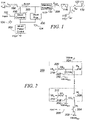
- FIGURE I is a block diagram of an RF power amplifier (PA).
- PA RF power amplifier
- the illustrated RF PA is quite general, in that varying the biasing of devices in a driver elements block 200, and/or varying details of the other blocks, will permit the RF PA illustrated in FIGURE 1 to operate in any of amplifier classes A, B, C, E, F, or, as described further herein, as an iClass amplifier.
- FIGURES 2-5 each show an exemplary circuit to implement one of the blocks shown in FIGURE 1 .
- An input 102 is provided to the PA with respect to a circuit reference, or common, 104.
- the input 102 generally comprises a properly biased signal at a center drive frequency, f 0 .
- the driver elements block 200 controls conduction between a drive output node 106 and the circuit common 104.
- the driver elements block 200 in conjunction with current from V DD via an RF choke (RFC) L s 108, provides a signal having a particular impedance Zdrive.
- Zdrive may vary with frequency; but will refer to the drive impedance at the center operating frequency f 0 , unless otherwise indicated.
- a shunt filter 400 is coupled between the drive output node 106 and the circuit common 104. Numerous different filtering arrangements may be used, some examples of which are described subsequently herein.
- An antenna 110 has a characteristic impedance Z out , generally 50 ⁇ (at the center frequency f 0 unless otherwise indicated).
- a block 300 is typically required to provide matching and coupling between the drive node 106 (at Zdrive) and the output at Z out .
- an output filter section such as the combination of L o 116 and C o 118 may typically be disposed in the signal path before an RF switch, S RF 120, which appropriately couples the output to the antenna 110.
- S RF 120 RF switch
- Power control may optionally be provided.
- a shunt power control block 500 which may provide a voltage offset between chassis ground 112 and circuit common 104 to reduce the amplitude of signals received by the antenna 110.
- a series regulator circuit such as items 1400-1401 in FIGURE 12 , is probably used more commonly.
- the monolithically integrated RF PAs, RF front ends, and RF transceivers described herein may be fabricated to operate at relatively high frequencies of at least 900 MHz and/or 2.4 GHz, and at moderate power levels. These designs are useful for transceivers having transmit power maximums of at least 0.5 W, 1 W, or 1.5 W RMS of RF output power delivered to the antenna connection when it is properly coupled to a matched antenna.
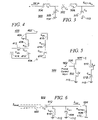
- FIGURE 2 is a simplified schematic diagram of a stacked-FET circuit according to an embodiment of the claimed invention, that may be used for the driver elements block 200 in the RF PA of FIGURE 1 , for controlling conduction between the drive output node 106 and the circuit common 104.
- the stack includes two or more FETs of the same polarity, i.e., all FETs in a stack are N-channel FETs, or all are P-channel FETs, or at least all FETs in a stack operate substantially similarly as each other.
- the FET stack 200 of FIGURE 2 is configured to control conduction between two nodes of an integrated circuit.
- a terminal Vdrive REF 202 is connected to one of the two nodes (e.g., circuit common 104 in FIGURE 1 ), while a terminal Vdrive 224 is connected to the other node (e.g., Vdrive 106 in FIGURE 1 ).
- Vdrive REF 202 will be connected to the more negative of the two nodes, for example to circuit common 104 in FIGURE 1 .
- the terminal Vdrive REF 202 is coupled to the source of a first FET of the stack 200 , M 1 204.
- the FET stack 200 is controlled by means of an input signal, relative to terminal Vdrive REF 202, that is coupled to the gate of the signal-input FET M 1 204 via an input terminal 206.
- the drain of M 1 204 is coupled to the source of a second FET M 2 208.
- the gate of M 2 208 is provided with a bias voltage VB 2 210 via a bias resistor RB 2 212, and is decoupled to Vdrive REF 202 via CG 2 214.
- these two FETs are sufficient, when properly configured to divide applied voltages so as to avoid exceeding breakdown limits of either device, to serve as a conduction controlling circuit to handle increased voltages in a circuit such as a PA or a quad mixer.
- one or more additional FETs of the same polarity are connected in series with M 1 204 and M 2 208.
- Such additional FETs are represented in FIGURE 2 by an Nth FET, M N 216.
- the drain of the last FET of the stack, M N 216 is coupled to the output terminal Vdrive 224.
- each additional FET Associated with each additional FET is a biasing voltage VB N 218, which is coupled to the gate of the FET via a bias impedance such as RB N 220, and a capacitor CG N 222 for coupling the gate to a voltage such that the FET is enslaved to conduction by the signal-input FET (here, M 1 204). As shown, enslaving is effected by coupling the gate of each additional FET to Vdrive REF 202.
- FET stacks with at least nine FETs in series have been fabricated or simulated, and stacks of even more series FETs are certainly possible.
- physical circuit couplings generally include finite capacitance, inductance, and resistance.
- impedance may be intentionally added to such couplings. For example, it may be desirable to more closely control a drive impedance, and to dissipate heat in specific resistive series coupling elements rather than within the FETs themselves. It may also be desirable to add impedance between the FETs of the FET stack 200 so as to tune the conductance of the drive circuit.
- the FETs of a FET stack may all have substantially similar voltage withstand capabilities, such as breakdown voltages V GS(br) , V DS(br) , and V DC(br) .
- these values will be similar from FET to FET.
- the breakdown voltages V GS(br) , V DS(br) , and V DG(br) may be approximately equal to each other. Proper biasing will usefully ensure that none of these breakdown voltages is exceeded during normal operation of the circuit. In some embodiments, with proper biasing, voltage excursions between Vdrive REF 202 and Vdrive 224 may be permitted to approach a sum of V DS breakdown voltages for each constituent FET of the stack.
- Biasing and coupling the FETs of a FET stack as described below may prevent voltages from exceeding any maximum allowable node to node voltage for any FET of the stack, even when the total voltage impressed from Vdrive 224 to Vdrive REF 202 is nearly equal to the sum of the maximum allowable V DS for the individual FETs of the stack.
- the maximum allowable voltage between any two nodes of the FETs i.e., V GS , V DS , and V DG
- V GS , V DS , and V DG are generally assumed to be substantially equal, both for the various nodes of each FET, and from FET to FET, which accords with an exemplary semiconductor fabrication processes.
- N-channel FET stacks may be applied to P-channel FET stacks with appropriate inversions of polarities and references.
- the impedance of the gate drive of M 1 may be selected according to ordinary transistor driving principles.
- V DS (max) is the same for all FETs of the stack.
- V DS for M 1 will therefore approximate (Vdrive-Vdrive REF )/N.
- the effective value of each biasing resistor RB x is selected to control a time constant, ⁇ GX , of the gate coupling.
- ⁇ GX is, approximately, the sum of effective capacitances of the gate coupling capacitor CG x plus the parasitic gate capacitances C GPX , multiplied by the series impedance to a biasing voltage.
- Vdrive REF Vpeak REF
- Vpeak Vpeak that is the maximum expected value of Vdrive
- VB x X Vpeak / 2 N
- each gate node (V GX ) is coupled via the capacitor C GX to the reference voltage Vdrive REF .
- Each gate node is also coupled to a DC bias voltage via a bias resistor.
- the effective drive voltage V GSX for each FET M x of the FET stack depends upon the voltage excursion of its source, V sx , in conjunction with the impedance from the source to the gate node, and from the gate node to AC ground. These impedances are dominated by the gate-source capacitance and the coupling capacitor CG x . Appropriate values for CG x may be determined as follows.
- the maximum voltage between each node pair of each FET is the same.
- the voltage excursions of the source of FET M 2 must therefore not exceed the maximum V DS for M 1 .
- the value of CG 2 . is unlimited, and desirably large, for effecting AC grounding of the gate of M 2 and thereby providing the largest common-gate drive signal to M 2 .
- V GS (max) will not be exceeded for M2 if the (DC) voltage on the gate is maintained within the range of the source voltage excursions.
- CG 2 values may need to be limited in a manner analogous to that described below for CG x for X from 2 to N.
- C OX for a particular FET M X is designated C OXX .
- the gate-source excursion ⁇ V GSX ( ⁇ V SX )/(1+C OXX /C GSX ). Presuming equal maximums for V GS and V DS , it is desired to limit ⁇ V GSX ⁇ Vpeak/N.
- FIGURE 3 shows an exemplary matching, coupling and filtering block 300, which, as shown in FIGURE 1 , may be disposed between the drive output node 106 and the antenna 110.
- the matching function transforms the typically 50 ⁇ characteristic impedance of the antenna, Z out , to the characteristic impedance of the drive output node 106 (both at the operating frequency f 0 ) in a manner well known to those of skill in the art.
- the coupling capacitor C C 302 blocks DC from the drive output node 106, and may be selected to have an impedance at f 0 that is less, and desirably much less, than the impedance to chassis ground 112, or to circuit common 104, from either side of the capacitor 302.
- the matching circuit 300 includes an "A" filter element comprising an inductor L A 304 and a capacitor C A 306, which may be fabricated as part of the integrated circuit.
- the matching circuit 300 also includes a "B" filter element comprising an inductor L B 308 and a capacitor C B 310 to chassis ground 112 (to which the antenna 110 of FIGURE 1 is referenced).
- the coupling capacitor Cc 302, as well as the inductor L B 308 and the capacitor C B 310 may be fabricated on an integrated circuit with the PA, but some of these devices are typically external to the integrated circuit.
- FIGURE 4 illustrates a shunt filter 400 that may be employed in an iClass PA such as illustrated in FIGURE 1 .
- a node 402 of shunt filter 400 may be connected to the drive output node 106 of FIGURE 1 , and an opposite node 404 may be connected to circuit common 104 of FIGURE 1 .
- the shunt filter 400 may provide local minimum impedances at each of one or more particular frequencies. The minimum impedances may be matched to the drive circuit impedance (as established, for example, by the drive elements 200 and the RF choke L S 108).
- the shunt filter elements may be fabricated as part of the integrated circuit that includes the drive elements 200, thus reducing loop areas of currents passing through the elements of the shunt filter 400.
- a shunt filter 400 for FIGURE 1 may be a "transmission line filter" fabricated of reactive elements that are substantially distributed over an appropriate length, for example 1 ⁇ 4 wavelength at f 0 .
- Such a transmission line may be coupled to circuit common via a resonant circuit having a maximum impedance at f 0 , such as a filter 600 as illustrated in FIGURE 6 and described in more detail hereinbelow.
- a resonant circuit having a maximum impedance at f 0 such as a filter 600 as illustrated in FIGURE 6 and described in more detail hereinbelow.
- Such a configuration for the shunt filter 400 provides local impedance minimums (approximately zero) at each even harmonic of f 0 , and local maximum impedances at each odd harmonic of f 0 . Stated more concisely, such a configuration may typically be said to reflect all odd harmonics, and to short all even harmonics, thus permitting operation as a Class F PA.
- the shunt filter 400 illustrated in FIGURE 4 for use in an iClass PA generally differs from such a transmission line filter.
- the shunt filter 400 may employ lumped, rather than distributed, elements. Consequently, local minimum impedances may occur at selected frequencies rather than at all odd, or at all even, harmonics of a resonant frequency (e.g., f 0 ).
- the filter may employ series resistive elements to intentionally establish a non-zero value of local minimum impedance. It may be useful, for example, to control the local impedance minimum values so as to match an impedance of the drive circuit at the corresponding frequency (or, alternatively, at f 0 ).
- a first shunt filter element includes L SF1 406, R SF1 408, and C SF1 410. These components establish a local minimum impedance at a particular frequency, with the impedance increasing for both higher and lower frequencies.
- a switch S1 412 in conjunction with an additional capacitor C SF3 414, represents an optional circuit for adjusting the frequency of the minimum impedance of the first filter element. As shown, the effective value of the series capacitor of the first filter element is increased when S1 is closed and C SF3 is disposed in parallel with C SF1 410.
- S1 412 may be a FET for electronically switching the frequency.
- C SF1 410, as well as optional C SF3 414, may be varactors (with the corresponding addition of an appropriate control circuit for the DC voltages on such varactors).
- the capacitor C SF3 414 may be disposed in series connection, rather than parallel connection, with C SF1 410, in which event the switch S1 may be configured to bypass the capacitor C SF3 414.
- analogous techniques may be employed to vary inductance, rather than capacitance.
- the switch S1 412 may selectably bypass a second inductive element, so as to vary the effective inductance of the first shunt filter element.
- the second shunt filter element comprises an inductor L SF2 416, a resistive element R SF2 418, and a capacitor C SF2 420.
- the resonant frequency of the second filter element (or, indeed, of any further filter element) of the shunt filter 400 may be varied by similar techniques as outlined above with respect to the first filter element. It may be useful to have a minimum impedance that is substantially resistive, and/or that is non-zero.
- the first and second filter elements are designed to provide local minimum impedances, at a second harmonic and a third harmonic of the operating frequency f 0 respectively, which are approximately equal to the drive circuit impedance. Though only two filter elements are illustrated, additional harmonics may desirably be treated with additional filter elements (not shown).
- FIGURE 11 is a schematic diagram of a circuit alternative for shunt filter 400 together with matching and coupling circuit 300.
- Zdrive and Z OUT of FIGURE 11 are connected as shown in FIGURE 1 .
- C C 302 is substantially the same as in FIGURE 3 , providing DC isolation of the PA from the antenna output.
- the shunt filter includes a parallel resonant circuit primarily consisting of C SF 980 and L SF 982, which together function as a tank circuit that is resonant at f 0 . All integer harmonic frequencies of f 0 are coupled through Rdrive 984, which is preferably selected to be approximately equal to the characteristic drive impedance of the PA switching circuit. Thereby, all harmonic frequencies of f 0 are terminated at the drive impedance.
- alternative filtering such as two parallel tank circuits each resonant near f 0 , may be disposed in series above Rdrive 984.
- Dual tank circuits may be configured either to resonate at substantially identical frequencies, thereby increasing the impedance at f 0 and reducing power loss at f 0 , or to resonate at slightly different frequencies, thereby broadening the range of frequencies at which the circuit has high impedance to ease manufacturing tolerances.
- a matching and filtering network 990 may be as illustrated in FIGURE 3 , except for two differences: first, coupling capacitor C C 302 is omitted, and second, C A 306, being on the antenna side of coupling capacitor C C 302, is coupled to earth ground 112 rather than circuit common 104.
- the two common references may be made effectively identical in some integrated circuit layouts.
- FIGURE 5 illustrates elements of one possible shunt power control circuit 500 for the PA of FIGURE 1 .
- a power control input 502 may establish a bias with respect to chassis ground 112.
- An inductive impedance Lgl 504 (which may reflect, for example, the inductance of a bond wire) is illustrated between chassis ground and the source of a power control FET M PC 506.
- a connection 508 may be coupled to circuit common 104 in FIGURE 1 .
- An inductance Lg2 510 typically exists in series with a bypass capacitor for the power control circuit, C PC 512. Assuming that the DC voltage V DD is with respect to chassis ground 112, the substantially DC voltage established across C PC 512 will reduce the effective supply voltage with respect to circuit common 104.
- the bias voltages on the FETs M 2 208 ... M N 216 may be adjusted. Efficiency will decrease, but power output will decrease more rapidly.
- Vdrive in iClass operation with harmonic termination
- a circuit may be configured as shown in FIGURE 7 , except that the effective average voltage at the gate of M 2 208 may be controllably reduced. This may be accomplished by making the value of RB 1 708 variable (e.g., by means of a parallel FET).
- the value of RB 1 708 may be reduced, and RB 1 708 may be coupled to a variable voltage source rather than to reference 202. Reducing the bias voltage will cause corresponding reductions in drive output voltages. As described below in more detail, the self adjusting bias supply circuit of FIGURE 7 will permit the bias on RB N to gradually follow the reductions in Vdrive(peak) that are caused by varying the bias voltage on the gate of M 2 .
- PA output power may also be controlled by varying the amplitude of the drive signal.
- the conduction impedance of the drive elements will be higher when driven with a lower amplitude rectangular wave, resulting in a smaller effective drive voltage.
- the efficiency of this technique is typically comparable to the efficiency of varying bias voltages.
- a series regulator circuit may be used to control PA output power either alone, or in conjunction with one or more other power control techniques.
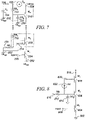
- FIGURE 6 is a simplified schematic diagram of a filter circuit 600 that may be employed in a manner similar to the shunt filter 400 in FIGURE 1 to form a versatile PA architecture.
- the drive output node 106 of FIGURE 1 may be coupled to a Zdrive node as an input to 600.
- the Zdrive node may be coupled via a 1 ⁇ 4 wavelength transmission line 602 and a coupling capacitor C C1 612 to an output filter section.
- the output filter section may comprise a parallel combination of L OF1 610 and C OF1 608, resonant at the operating frequency f 0 .
- the output filter section of FIGURE 6 is typically not part of the PA integrated circuit, and thus is referenced to chassis ground 112 rather than to circuit common.
- a Z OUT node 604 may be coupled to a further output filter section 116-118, an RF switch 120, and antenna 110 as shown in FIGURE 1 .
- a matching network (not shown) may also be required, similar to that illustrated in FIGURE 3 with the coupling capacitor C C 302 omitted.
- Such further filtering and matching circuits, or a transmission line coupled thereto, will ideally appear to the filter circuit 600 as a resistive impedance R OUTequiv 606 at the operating frequency f 0 .
- the circuit of FIGURE 1 may be operated as an RF PA of Class A, Class B, Class C, Class E or Class F.
- Class A operation the input signal 102 is sinusoidal and does not cause the current through M 1 202 of FIGURE 2 to go to zero.
- Class B operation the input signal 102 is sinusoidal but M 1 202 conducts only 50% of the time (conduction angle 180 degrees). Operation may be Class C, with a conduction angle less than 180 degrees, which yields some efficiency improvement as compared to the Class B operation.
- the FETs M 2 to M N are enslaved to M 1 , and the FET stack of FIGURE 2 functions substantially as a single device.
- the circuit of FIGURE 1 may also be operated as an iClass PA in a configuration related to Class F but having dissipative termination for harmonics of the operating frequency.
- the circuit of FIGURE 1 may also be operated as a Class F RF PA.
- the input signal is preferably a square wave having a duty cycle that causes the circuit 200 to conduct at precisely a 50% duty cycle.
- the output voltages resulting from Class F operation generally increase substantially when the conduction duty cycle deviates from 50%.
- ordinary manufacturing component variations tend to cause the duty cycle to deviate from 50%, and consequently the circuit may not readily be able to safely and reliably utilize the full voltage withstand capability of the drive element(s).
- Embodiments of a FET stack may include a signal-input FET that receives a drive signal coupled to its gate with respect to a reference voltage that is coupled to its source.
- the remaining FETs of the stack may be enslaved to the signal-input FET, such that they conduct under the control of conduction in the signal-input FET.
- the method by which the other FETs of a FET stack are enslaved to the signal-input FET must cooperate with the method employed to properly bias the FETs. Accordingly, enslavement and biasing are addressed together.
- RF PAs generally according to FIGURE 1
- the peak voltage of drive output node 106 will often exceed twice the available supply voltage V DD 114.
- bias voltages as required for the driver elements of FIGURE 2 may not be readily available. This lack may be remedied by recourse, for example, to a charge pump.
- a charge pump that is preferred from the standpoint of minimal noise generation is described in commonly owned and copending U.S. Patent Application 10/658,154 , "Low-Noise Charge Pump Method and Apparatus".
- a low-current voltage source may be readily established at any desired voltage. Such voltage source may be provided, as needed, to any of the bias voltage inputs VB 2 210 to VB N 218 in FIGURE 2 .
- FIGURE 7 illustrates a self-adjusting bias supply that may be employed to bias the FETs of a FET stack.
- a signal input 206 is coupled to the gate of a signal-input FET M 1 204.
- the source of the FET M 1 204 is coupled to Vd REF 202, while its drain is coupled in series with each subsequent FET of the stack, including M 2 208 ... M N 216.
- the drain of the last FET of the stack, M N 216 is coupled to Vdrive 224.
- a diode (or equivalent) D B 702 charges a bias supply capacitor C B 704 to Vbias 706.
- Vbias will charge to approximately Vpeak, the peak value of Vdrive 224 with respect to Vd REF 202. If a time constant associated with C B 704 is sufficiently long, then Vbias will remain substantially at this value.
- the time constant is the product of the capacitance of C B 704 multiplied by the resistance, to Vd REF 202, of the resistive voltage divider having N resistors including RB 1 708, RB 2 710, ... , and RB N 712. The total resistance of this voltage divider may be designated R B sum.
- X represents the position of the particular FET in a stack
- a significant ripple voltage is not necessarily a problem, and C B may desirably assume even smaller values if rapid self-adjustment response is required. Indeed, in view of the filtering effected by each gate bypass capacitor CG X in conjunction with RB X(equiv) , an average value is the main consideration for Vbias. However, if the average value of Vbias is permitted to decline significantly below Vpeak for any reason, including the presence of substantial ripple on C B , the skilled person will understand that the resistive divider values should be adjusted accordingly.
- FIGURE 8 illustrates an alternative for providing both bias and gate coupling for FETs M 3 and above (X ⁇ 3).
- a reference 802 is coupled to the source of a signal-input FET M 1 804, the gate of which is coupled to an input signal 806.
- the drain of M 1 804 is coupled to the source of a second FET M 2 808.
- a bias voltage is applied to a bias input 810, which is coupled via a bias resistance RB 812 to the gate of M 2 808, and to a relatively large capacitance CG 2 814.
- the drain of M 2 808 is coupled to the source of a third FET of the stack, M 3 816.
- the drain of M 3 816 may be coupled to a further FET stage, if present However, the drain of the FET of the last stage, M 3 816 as shown in FIGURE 8 , is coupled to an output node Vdrive 818.
- the gate 820 of FET M 3 816 may be coupled to the base of the preceding stage FET M 2 808 via a zener diode DZ 822.
- DZ 822 may have a conduction threshold knee at approximately the maximum desired value for V DS of M 3 816. (A circuit operating similarly to a zener diode may be used instead of DZ 822.)
- Additional FET stages designated by subscripts "Y" may be added. For such additional stages, corresponding additional zener diodes may be employed in like manner as DZ 822, i.e., anode to the gate of additional FET M Y , and cathode to the gate of M (Y-1) .
- N-FETs N-channel FETs
- P-FET stacks may be fabricated analogously, by reversing the polarity of each voltage and polarized component associated with the stack.
- the P-FET stack reference voltage will generally be coupled to the source of a first, signal-input FET M P1 .
- Such inverted circuits will operate according to substantially the same principles as the N-FET stack circuits described above.
- Vdrive 818 may be negative with respect to reference 802 in FIGURE 8 if all FETs are P-channel, and the zener DZ 822 connection is reversed (anode and cathode exchanged).
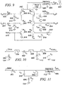
- FIGURE 9 is an exemplary circuit that employs both an N-channel FET stack comprising N-channel FETs M N , 902, M N2 904 and M N3 906, plus a P-channel FET stack comprising P-channel FETs M P1 908, M P2 910 and M P3 912.
- an input square wave may be provided with respect to common 914 at the input 916 to the N-FET stack, and coupled to an input for the P-FET stack on the gate of M P3 912 via a capacitor C GP1 918.
- a bias voltage set for example to one half of V GS (on) below the P-FET stack reference V DD 930, may be provided for M P1 908 via a bias resistor R BP1 920.
- the capacitor C GP1 918 and the bias resistor R BP1 920 may be deleted, and the input 916 and the gate of M P1 908 may each be driven, instead, by means of an appropriate non-overlap clock generator (not shown).
- the gate of M N2 904 is coupled to common ( i . e ., decoupled) via a capacitor C GN2 922 having a relatively large value, and may be biased to about (V DD /3) volts via a bias resistor R BN2 924.
- the gate of M N3 906 is decoupled to common via a capacitor C GN3 926 having a value calculated as described with respect to FIGURE 2 , and may be biased to (V DD /2) volts via a bias resistor R BN3 928.
- the P-FET stack is controlled analogously as the N-FET stack.
- the polarities of the bias voltages are inverted, and referenced to the "reference voltage" of the P-FET stack, which in this case is V DD 930.
- V DD 930 the reference voltage of the P-FET stack
- decoupling capacitors 932 and 936 may alternatively be connected to circuit common 914.
- the gate of M P2 910 is decoupled to V DD via a relatively large capacitor C GP2 932, and biased to about 2/3 V DD via a bias resistor R BP2 934.
- the gate of M P3 912 is decoupled to V DD via a capacitor C GP3 936.
- the gate of M P3 912 is biased to about V DD /2 via a bias resistor R BP3 938.
- An output voltage Vdrive 940 will be driven between common and V DD , according to whether the N-FET stack is conducting or the P-FET stack is conducting.
- the output Vdrive 940 may be shunt filtered by a shunt filter 950, and may be processed by a matching and coupling circuit 960, as described below in more detail with respect to FIGURE 10 . From the matching and coupling circuit 960 the signal may proceed to an antenna 942, typically via a transmission line, one or more further filter sections, and an RF switch (not shown).
- the shunt filter 950 of FIGURE 9 may be similar to that shown in FIGURE 4 , or that shown in FIGURE 6 .
- the matching and coupling circuit 960 of FIGURE 9 may, for example, be similar to that shown in FIGURE 3 .
- FIGURE 10 illustrates filtering that may be employed for both blocks 950 and 960 in the circuit of FIGURE 9 .
- the capacitor C S 952 may serve as the shunt filter 950.
- the remainder of FIGURE 10 may function as the matching and coupling circuit 960 of FIGURE 9 .
- An inductor L C 954 may comprise a physical coupling connection.
- a coupling capacitor C C 962 serves to block DC.
- L A 964, C A 966, L B 968 and C B 970 may be configured for matching to the output impedance Z OUT . which is typically 50 ohms.
- An RF transceiver such as the dual-band RF transceiver represented in FIGURE 12 , typically includes a received-signal amplifier such as items 1226 or 1256 of FIGURE 12 .
- a received-signal amplifier is typically a low noise amplifier (LNA), and is employed to condition signals received from the antenna.
- An RF front end may be considered to be an RF transceiver circuit that does not necessarily include an LNA.
- discrete integrated circuits In most RF transceivers, discrete integrated circuits must be combined in a module to fabricate a complete RF front-end section. Typically, at least the antenna switch will be fabricated on a different, separate integrated circuit (IC) from the PA, and often many more discrete integrated circuits must be connected via off-chip wiring to fabricate an RF front end module.
- IC integrated circuit
- Each such discrete integrated circuit must be defined by particular performance requirements which ensure that the module functions properly even when the discrete integrated circuits which it comprises are from different lots, or have been designed and manufactured differently from other integrated circuits that perform the same tasks. Such performance requirements, which are thus developed to achieve mix-and-match flexibility and reliability, may well exact a cost for the discrete ICs that are combined in these devices.
- PAs in multiple-IC transceiver modules typically produce a signal of substantial power on demand.
- An antenna switch unit couples an antenna (more precisely, an antenna connection) to either a transmit signal matched to the expected antenna impedance (e.g. , 50 ohms), or to a receive signal input.
- a transmit signal matched to the expected antenna impedance (e.g. , 50 ohms)
- the impedance reflected to the antenna connection point from the antenna connecting line to vary drastically from its expected value.
- a large voltage standing wave (VSW) may be caused by the resulting mismatch between that reflected impedance, and the expected value to which the transmit signal has been matched. Voltage excursions much larger than those expected during normal operation may be generated as a consequence of such mismatch-induced VSWs.
- Voltage withstand requirements for antenna switches are typically set much higher than normal peak operating voltages to avoid damage under such mismatch conditions.
- the IC area occupied by switching devices (such as FETs) in a power-switching circuit, such as an antenna switch, may increase as the square of the voltage they are capable of withstanding. Thus, halving the required withstand voltage may reduce the switch device area to one fourth. Moreover, because these devices dominate the IC area used by an antenna switching circuit, a very substantial saving in IC area (and thus in manufacturing cost) may be realized by reducing their required withstand voltage. Such reduction may not be practical when discrete ICs must be coupled to fabricate an entire transceiver. However, a single IC that includes all devices from a PA, through an antenna switch, and to an antenna connection, may take advantage of reliable internal coupling and close device matching to protect against high mismatch-induced VSWs. Due to these advantages of integration, substantial savings in device area can be realized as compared to combining discrete ICs to fabricate a comparably-performing transceiver.
- FIGURE 12 is a simplified block schematic diagram of the primary RF sections of a dual-band transceiver that is configured to benefit from such internal protection.
- a low-level signal at a first operating frequency f O1 is coupled to an input node 1202 from a source which may (but need not) be on the same IC chip.
- the signal is amplified through any suitable amplifier, as indicated by amplifier 1204.
- the signal produced by the amplifier 1204 may deviate considerably from a preferred rectangular shape if a pulse adjustment circuit 1500 is provided to improve rectangularity, and preferably to also adjust the duty cycle, of the waveform that is ultimately coupled into a power amplifier (PA) 1206.
- PA power amplifier
- the output of the pulse adjustment circuit 1500 is the input to the PA 1206, which draws power from a supply V DD 114 via supply conditioning elements, including a series regulator 1400 and an RF choke (RFC) L S 108, to generate a PA output signal.
- the PA output signal has a characteristic impedance resulting from the input signal, the PA circuit elements, and the supply conditioning elements, and generally differs from the impedance expected at the antenna node 1214.
- a coupling, matching and filtering network may be needed, for example as represented by a block 1210.
- Such a network may couple the PA output signal to the antenna switch while blocking DC current, and may transform the PA output impedance to the desired antenna node impedance (e.g., 50 ohms).
- the antenna switch 1700 selectably couples the signal to the antenna node 1214, from whence it may be coupled, for example by transmission line, to an antenna that may be separated from the IC chip.
- An output sensor 1600 may be coupled to the antenna node 1214, sensing the electrical stress and providing a signal that will cause the PA to reduce its output if the electrical stresses are excessive.
- the output 1220 of output sensor 1600 is coupled to an input "B" of a PA control block 1300.
- An "A" input 1224 to the PA control block 1300 may receive an amplitude control signal to adjust the envelope amplitude of the PA output signal. This input may also be used to restrict, or even to terminate, output from the PA.
- Both the "A” and “B” inputs may affect an output “D” that is coupled from the PA control block 1300 to the series regulator block 1400.
- a “C” input 1222 to the PA control block 1300 may be provided with information, or a signal, that controls an “E” output from the block 1300.
- the "E” output may be coupled to the pulse adjustment circuit 1500 to control the duty cycle of the rectangular wave that is input to the PA 1206.
- Duty cycle control may, for example, provide another means to reduce the power level of the PA output signal.
- the signal path from 1202 may be tuned for a first band of operating frequencies, which include f O1 .
- the antenna switch 1700 may selectably decouple the antenna node 1214 from the first-band transmit signal on input "A,” and couple the antenna node instead to output "B" so as to deliver a signal received from the antenna to a receive preamplifier 1226 for a first receive band.
- the receive preamplifier 1226 (as well as 1256) is preferably a low noise amplifier (LNA). LNAs are not necessarily included in integrated front ends as described herein, though they typically are included in complete transceiver circuits. The output from receive preamplifier 1226, if present, may be delivered to further first receive band circuitry either on or off the same IC chip.
- the antenna switch 1700 may similarly selectably couple the antenna node 1214 to a second receive band preamplifier 1256 to amplify a signal from the antenna to a second receive band output node 1258. That output may be delivered to further second receive band circuitry either on or off the IC chip.
- a transmit signal at a second operating frequency f O2 in a second operating frequency band may be provided to an input 1232, and amplified by an amplifier 1234.
- the duty cycle and waveform of the signal output from the amplifier 1234 may be conditioned by a pulse adjustment 1501 under control of a PA control block 1301, and then delivered as an input to a second band PA 1207.
- the second band PA 1207 will generate a second-band PA output signal using power that is provided from V DD 114, as limited by a series regulator 1401 under control of the PA control block 1301, via an RF choke 109.
- the second-band PA output will have a characteristic impedance, and will be coupled to the "D" input of the antenna switch 1700 via a block 1211 that couples the signal, matches the PA output and antenna node impedances, and filters the output signal.
- the antenna switch 1700 may be controlled to couple the "D" input to the antenna node 1214, from whence the signal will be delivered to the antenna 1216.
- the output 1220 of the output sensor 1600 may be coupled also to a "B" input to the second-band PA control block 1301, whereby excess output voltage will cause the second-band PA output signal to be reduced to safe levels.
- the second-band PA control block 1301 may also accept an envelope-control signal at an "A" input 1254, as well as a duty-cycle control signal at a "C" input 1252.
- control circuitry is preferably enabled only when the associated PA is active.
- Exemplary circuitry for a PA control block such as 1300 or 1301, is shown in FIGURE 13 .
- the PAs 1206 or 1207 may be fabricated as described for Driver Elements 200 of FIGURE 1 , together with a shunt filter, such as block 400 of FIGURE 1 or the appropriate elements of FIGURE 11 .
- Coupling, matching and filtering circuits 1210 and 1211 may be fabricated as described above for FIGURE 3 , or FIGURE 10 , or in any other manner to obtain similar coupling, matching and filtering effects. Note that if a circuit as shown in FIGURE 11 is to be employed, the coupling capacitor 302 will be disposed before the shunt filter, and the matching and filtering will be provided subsequently, as in block 990.
- FIGURE 13 illustrates exemplary circuitry for a PA control block 1300.
- An enable input "A” 1302 may be coupled directly to a FET 1304, such that if input 1302 is approximately ground potential, an output “D” 1306 can draw no current. Conduction into the output “D” 1306 may control the PA output power via a series regulator, such as shown in FIGURE 14 , such that when output 1306 conducts no current, no current will be provided to the PA, reducing output power to zero as discussed below with respect to FIGURE 14 .
- FET 1308 is biased by resistors 1310 and 1312, which may have equal values, a nominal value such as 30-50 k ⁇ being selected for engineering convenience. This configuration protects low-voltage FETs, ensuring that V GD , V GS , and V DS for all of FETs 1304, 1308 and 1314 do not significantly exceed V DD /2,
- a power sense input “B” 1316 may be coupled to resistor 1318.
- Resistor 1318 may be about 30-50 k ⁇ , and reasonably equal to a resistor 1320 to establish unity gain for op amp 1322.
- a power set input “C” 1324 may be set, in one embodiment, from 0V to 2 ⁇ Vth (FET threshold voltage), where Vth may be 0.4 to 0.7V, nominally about 0.5V, and is consistent within the circuit.
- the noninverting input of op amp 1322 is prevented from exceeding this voltage range by means of a resistor 1326 (e.g., 30-50 k ⁇ ) together with diode-connected FETs 1328 and 1330, thus limiting the maximum power that may be selected.
- circuit values, and circuit design may be adjusted so as to achieve a selectable output power up to a fixed circuit design maximum.
- one or both diode-connected FETs 1328 and 1330 may be replaced by a network that includes a bandgap reference, for example to increase accuracy of power settings and output voltage limits.
- Many other techniques may be employed to achieve similar effects.
- the PA control block 1300 also provides an output "E" 1512 to control the duty cycle adjustment effected by the pulse adjustment circuit 1500 of FIGURE 12 .
- a reference voltage which may be adjustable according to factors such as fabrication process parameters, is provided at an input 1332. This voltage is doubled by an op amp 1334 under control of equal-valued resistors 1316 and 1318. Of course, in other embodiments the gain of circuitry such as shown in FIGURE 13 will likely be different, and resistors setting such gains, for example 1316 and 1318, will accordingly differ in value. By reducing the duty cycle somewhat, the PA output power may be correspondingly reduced, and by reducing it to zero the PA output may be suppressed entirely.
- a reference voltage provided to an input 1322 of an amplifier 1320 the gain of which may be controlled in the usual manner by resistors 1324 and 1326, may serve to establish the voltage at output "E" 1512 to control duty cycle of the output of block 1500.
- FIGURE 14 illustrates an exemplary series regulator circuit 1400 for limiting the effective voltage provided to the PA, and thus limiting the PA output amplitude.
- the voltage provided to input 1306, as compared to V DD is divided via resistors 1406 and 1404 to control a P-channel FET 1402 and also protect FET 1402 from excessive voltage between any two nodes.
- a P-channel FET 1408 is biased by resistors 1410 and 1412 so as to divide maximum voltages that are generated between V DD and an output 1414, somewhat equally between FETs 1402 and 1408,.
- the output 1414 provides power to the PA via an RF choke.
- the FETs 1402 and 1408 may, for example, have V GS threshold voltages of between -0.4V and -0.7V.
- Resistors 1404, 1406, 1410 and 1412 may all be substantially equal, with a magnitude selected for engineering convenience to be, for example, 30-50 k ⁇ . These exemplary values and relative values may be varied for engineering convenience.
- FIGURE 15 is a schematic representation of an exemplary signal conditioning circuit 1500.
- An input signal may be provided on an input node 1502, and coupled via a diode-connected FET 1504 to the input of an inverter 1506.
- the input signal voltage, plus the V DS threshold of FET 1504 is less than the threshold of the inverter 1506, the output of inverter 1508 will be low.
- the FET 1504 will cease conducting. Thereafter, even if the voltage of input 1502 is quite high (e.g., V DD ), current from the input will be limited by P-channel FET 1510 under control of an input voltage 1512.
- Such current through the FET 1510 must charge a capacitor 1514 (which may be a metal-insulator-metal or "MIM" capacitor of about .025 to .05 pF) until the input to inverter 1506 rises above its switching threshold. At that point the inverters 1506 and 1508 will change state rapidly due to positive feedback via the capacitor 1514, providing square edges at an output node 1516, rise and fall times being limited primarily by delays through the inverters 1506 and 1508.
- the signal at the input 1502 is a roughly rectangular wave of about 50% duty cycle, as in a preferred embodiment, the voltage at the control input 1512 may be adjusted such that the output duty cycle is reduced from 50% to an arbitrarily lower value that may reach zero.
- the input signal may be configured to have a duty cycle exceeding 50% if a wider range of output duty cycle is desired.
- FIGURE 16 is a schematic of exemplary circuitry 1600 for sensing peak voltage at a sense node 1602, which may for example be connected directly to antenna node 1214 of FIGURE 12 .
- An input divider may be used as shown to sense relatively high voltages.
- Four roughly equal resistors 1604, 1606, 1608 and 1610 having a relatively low resistance, such as 1 k ⁇ , may be used.
- Diode-connected FET 1612 conducts when this voltage is high, providing current through a resistor 1614 of about 24 k ⁇ to a capacitor 1616 of about 1 pF.
- Many other values may be used, so long as the time constant established by resistor 1614 and capacitor 1616 is much smaller than the duration of any event that could cause the output voltage to rise (for a given level of PA output signal).
- an antenna mechanical event that caused the antenna impedance to vary drastically from the design value, thereby causing a high voltage standing wave to appear will take at least milliseconds to occur.
- the time constant of approximately 24 nS of the exemplary circuit 1600 is well below such an event duration.
- the corner frequency due to these components should generally be well below both the first and second band operating frequencies f O1 and f O2 , in order to avoid circuit oscillations. If event durations may approach 1/f O , then other common circuit design considerations may require a more complicated circuit to avoid oscillation while ensuring that the response is sufficiently fast to prevent excessive voltages.
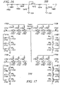
- FIGURE 17 is a simplified schematic of exemplary circuitry 1700 for an antenna switch. Further details regarding design and fabrication of such an RF switch may be found in U.S. Patent No. 6,804,502, issued October 12, 2004 and entitled “Switch Circuit and Method of Switching Radio Frequency Signals.” Circuitry to provide control signals is not shown. Moreover, the control voltages should preferably be either "high,” nearly V DD , or "low” at nearly -V DD . To generate -V DD control voltages, a negative voltage generator will be helpful, preferably a low-noise circuit such as described in copending, published U.S. Patent Application No. 10/658,154, filed September 8, 2003 and entitled “Low Noise Charge Pump Method and Apparatus.” Such a low-noise charge pump is important for avoiding unintended emissions from the antenna.
- a port node 1780 is the common connection of the switch 1700.
- the common connection of the switch 1700 is coupled to the antenna node 1214.
- the common connection is generally coupled to only one RF port (port A 1710, port B 1730, port C 1750, or port D 1770) at a time.
- Each RF port has a corresponding "+” control node and a corresponding "-" control node.
- the "+" control nodes are nodes 1708, 1728, 1748 and 1768, respectively, while the "-" control nodes are nodes 1718, 1738, 1758 and 1778, respectively.
- a "high” voltage ( ⁇ V DD ) is applied to the port's corresponding "+” control node, while a “low” voltage ( ⁇ -V DD ) is applied to the port's corresponding "-” control node.
- a "low” voltage is applied to each "+” control node corresponding to another RF port, and a “high” voltage is applied to each "-" control node corresponding to another RF port.
- a "high” voltage is applied to control nodes 1708, 1738, 1758, and 1778, while a “low” voltage is applied to all other control nodes (1718, 1728, 1748 and 1768).
- Every resistor will typically have the same value. In some embodiments, the value will be roughly 30-50 k ⁇ .
- the resistor is selected such that the time constant of the parasitic gate capacitance of a FET (e.g. M1 A 1701), in conjunction with the value of its corresponding gate resistor (e.g. 1704) is much greater than 1/f O , where f O is the lowest significant frequency of the RF signal being controlled.
- the illustrated configuration serves to divide the voltage appearing across FET stacks (such as the stack consisting of FETs M1 A , 1701, M1 B 1702 and M1 C 1703, the stack consisting of FETs M2 A , 1704, M2 B 1705 and M2 C 1706, and so on) uniformly, reducing compression effects.
- the FET stacks (such as FETs 1701, 1702 and 1703) that provide the switching functions may include more or less than the three devices that are shown for illustration; stacks of at least nine devices have been successfully fabricated. Due to the voltage stress distribution uniformity, a wide range of signal voltages and fabrication process parameters may be accommodated.
- the integrated circuits may be fabricated in accordance with ultrathin silicon on sapphire processing as described in U.S. Patent No. 5,663,570, issued September 2, 1997 and entitled "HighFrequency Wireless Communication System on a Single Ultrathin Silicon On Sapphire Chip.”
- SOI semiconductor-on-insulator
- mixers may be incorporated on such a device, enabling integration of more portions of transmission signal processing.
- Phase locked loops may further enhance the ability to generate the transmission signal on the same monolithic IC as the RF front end or transceiver.
- Additional types of filters may be useful, for either or both of receive and transmission processing.
Description
- This invention relates broadly to integrated electronic circuits, and more specifically to RF transceiver circuitry.
- Wireless communications devices, especially handheld devices, are undergoing sustained development. Perhaps more than any other factor, the extreme popularity of cellular mobile telephones has motivated improvements in efficiency, speed, size and cost-effectiveness for RF transmission circuits in handheld devices. Enhancing the efficiency of such circuits is highly desirable so that the size of the required batteries may be reduced, while their life is extended. Cost-effectiveness is clearly always desirable for consumer products, particularly when such products require periodic replacement to stay abreast of changes in the technology. The steady advance of functionality in cellular telephones, combined with consumer preferences for light and small devices, puts a premium on reducing the volume required for RF transmission circuits. Additionally, transmitters must meet stringent emission limits, which have been established in order to facilitate high communication density at minimal power levels.
- Most wireless communication units, such as cellular telephones, comprise at least one RF transceiver. A communication device, such as a cellular telephone, may comprise a multiplicity of RF (radio frequency) front end circuits, which are of primary interest herein. RF front end circuits (or subcircuits) typically include an RF transmit signal amplifier, a Power Amplifier (PA), a matching and filtering section, an antenna switch, and may include a received signal amplifier. A complete transceiver generally also includes a low-noise amplifier for the received signal. Of these circuits, the PA subcircuit is typically the most power-consuming portion of such transmitters, and, also typically, is the source of the most significant unintended or "spurious" emissions. In order to extend battery life, to meet stringent spurious emissions standards, and to minimize the cost of these high-volume consumer items, there is a need to improve the speed and efficiency, while reducing spurious emissions and manufacturing costs, for such PA subcircuits. Due to their need to handle high power, the PA and antenna switch subcircuits consume the most integrated circuit area. Manufacturing costs for integrated circuits are strongly dependent on the amount of device area required for each circuit Consequently, substantial reductions in the area required for the various RF transceiver subsections will generally lead to commensurate reductions in manufacturing costs for transceiver circuits.
- A range of PA topologies have been developed, each having different advantages. For example, PAs of class A, B, C, D, E and F are well known in the art. The primary amplifying devices in PAs of classes A-C are designed to operate in an "active" region of their operating range, thus intentionally conducting current while voltage is present across the device.
- PAs of classes D, E and F attempt to reduce the power loss caused by such linear operation by employing amplifier devices as switches that minimize operation in active regions, rather than as linear amplifiers. However, the pulse-type outputs from such amplifiers generally require extensive filtering in order to establish a narrow-band sinusoidal output, as is typically required. While normal operation of PAs in classes D-F does not intentionally cause drive element devices to conduct while voltage is present across the devices, even switched devices consume real power due to current flowing while voltage is present during finite switching periods. Moreover, compared to drive devices in analog PAs operating at the same transmission center frequency, drive devices in class D-F switching circuits must often operate at much higher frequencies. The higher frequency signals include significant energy at undesired frequencies, and such undesired signal energies not only consume circuit power, but also require filtering to meet emission limits.
- Integration of devices is generally desirable in order to improve various features of the resulting product, such as operating frequency and reliability, and may also reduce overall manufacturing costs, as well as likely reducing the volume occupied by the circuits. Field Effect Transistors (FETs) are extremely popular for both linear amplification and switching purposes in integrated circuits. However, integrated circuit (IC) FETs have a limited capability to withstand voltage between any two nodes, including gate-source, gate-drain, and drain-source node pairs. Such voltage withstand limitations may particularly impair the usefulness of IC FETs in high power switching circuits, in which inductive voltages may greatly exceed the supply voltage. As a particular example, the transmission output power capability of an RF PA is highly dependent upon the amplitude of the output voltage. One of the difficulties with existing PA technologies is that many otherwise desirably high-speed devices are fabricated using processes that tend to yield FETs having relatively low breakdown voltages. It is very desirable to solve this problem ant thereby provide a wider voltage range while retaining other desirable integrated device features. Such a solution enables integration on monolithic integrated circuits of power and control features that previously required separate processing, such as PA features and RF switch features. Integration of interacting circuits that were previously discrete will enhance yield and predictability, due to the process matching that is inherent in monolithic integration.
-
US 6,137,367 discloses simplified, efficient multiple-transistor power amplifiers that provide high power and high impedance while avoiding the use of RF power divider and combiner circuits. The input signal is directly applied to a first transistor, amplified, and supplied to the succeeding transistor, and so on, for amplification in series. Feedback is provided between the drain of the last transistor and the gates of all the transistors. Series connection of the transistors allows their power outputs and their output impedances to be summed, such that no RF output combiner is required. In a first high voltage embodiment of the amplifier of the invention, e.g., as used for satellite transmission, bias voltage is provided in series. In a second low voltage embodiment, suitable for use in cordless telephones and other battery-powered equipment, bias voltage Vds is provided separately across the drain and source terminals of each transistor, through paired chokes. -
US 2002/079971 discloses an integrated circuit chip that includes a cascode amplifier having a first NMOS transistor with the gate receiving an input signal a source connected to ground through an inductance and a drain connected to the source of a second NMOS transistor. The drain of the second transistor is connected to a supply voltage through another inductance. The gate of the second transistor is connected to a DC bias voltage through a resistor and is connected to a first plate of an on-chip parallel plate capacitor. The other plate of the capacitor is connected to a wirebond pad for connection to a circuit board through a bond wire. The capacitor together with the inductance of the bond wire form a short circuit at the operating voltage of the amplifier. -
US 5,945,879 discloses a microwave power amplifier comprised of a plurality of series connected amplifier stages. Each stage is provided with a local negative feedback. The addition of the local voltage feedback distribution networks provide correct voltage distribution and equal current distribution for all transistors, such that the peak-to-peak voltage and current swings of each transistor can be set simultaneously to the values required for efficient amplifier operation. The method applies to both FETs and bipolar transistors. The series connected microwave power amplifier is thus characterized as a stack with local voltage feedback networks which provide an equal distribution of voltage across the transistors in the stack. The amplifier stages can be biased and tuned to collectively operate either as a class A or B amplifier - Methods and circuits are described herein that facilitate the fabrication of all of the transceiver RF circuits of a dual-band transceiver onto a single integrated circuit, thereby solving the problems and gaining the benefits noted above. Many of the benefits are achieved by integrating even the front-end portions of transceivers that do not necessarily include dual-band operation. One or more alternatives are described for each of numerous subcircuits (or corresponding methods), and a fully integrated RF front end, or an integrated RF transceiver, may be fabricated by using any compatible one of such alternatives for each section of the transceiver. Moreover, several of the subcircuits (or corresponding methods) that permit an integrated RF transceiver to be realized are also useful in other contexts, often independently of other RF transceiver subcircuits. Thus, various subcombinations of features described herein constitute useful inventions in their own right. Combined, various aspects of these subcombinations together achieve an integrated dual-band RF transceiver having all of the benefits noted above. Particularly notable among the independently useful subcircuits are stacked-FET RF switches and particular PA circuit topologies. Finally, the integration of certain RF transceiver subsections permits efficiencies in manufacturing without compromising safety and reliability of the final product.
- The invention is defined by the features of the enclosed claims. A combination of methods and/or circuits is described that enables the fabrication of a self-protected monolithic integrated circuit including all of the RF front-end sections of a communications transceiver. Such self-protected RF front-end circuits particularly include those sections, from a Power Amplifier (PA) through an antenna connection, that permit efficient internal protection from overload due to an improper, missing or damaged antenna.
- Embodiments of the present invention will be more readily understood by reference to the following figures, in which like reference numbers and designations indicate like elements.
-
FIGURE 1 is a block schematic diagram representative of some types of RF power amplifier (PA) circuitry. -
FIGURE 2 is a generalized schematic diagram of a stacked-FET control circuit useable with a PA such as shown inFIGURE 1 . -
FIGURE 3 is a simplified schematic diagram of an impedance matching and coupling bandpass filter useable in a PA such as shown inFIGURE 1 . -
FIGURE 4 is a simplified schematic diagram of a shunt filter useable in a PA such as shown inFIGURE 1 . -
FIGURE 5 is a simplified schematic diagram of a shunt power control circuit useable in a PA such as shown inFIGURE 1 . -
FIGURE 6 is a simplified schematic diagram of an output filter for Class F operation of a PA such as shown inFIGURE 1 . -
FIGURE 7 is a schematic diagram illustrating alternative biasing features for a stacked-FET amplifying circuit. -
FIGURE 8 is a simplified schematic diagram illustrating an alternative method of biasing FETs of a FET stack. -
FIGURE 9 is a simplified schematic diagram of a Class D PA employing complementary stacked-FET drive elements. -
FIGURE 10 is a schematic diagram of exemplary output filtering for a Class D PA such as represented inFIGURE 9 . -
FIGURE 11 is a simplified schematic diagram of a harmonic termination shunt filter useable in a PA such as shown inFIGURE 1 . -
FIGURE 12 is a simplified schematic diagram of an integrated dual-band RF transceiver. -
FIGURE 13 is a schematic diagram of an exemplary PA output power supervisor for directing output power levels in the transceiver ofFIGURE 12 . -
FIGURE 14 is a schematic diagram of an exemplary series output regulator for the transceiver ofFIGURE 12 . -
FIGURE 15 is a schematic diagram of an exemplary pulse width controller for the transceiver ofFIGURE 12 . -
FIGURE 16 is a schematic diagram of an exemplary output voltage detector for the transceiver ofFIGURE 12 . -
FIGURE 17 is a schematic diagram of an exemplary dual-band antenna switch for the transceiver ofFIGURE 12 . -
FIGURE I is a block diagram of an RF power amplifier (PA). The illustrated RF PA is quite general, in that varying the biasing of devices in a driver elements block 200, and/or varying details of the other blocks, will permit the RF PA illustrated inFIGURE 1 to operate in any of amplifier classes A, B, C, E, F, or, as described further herein, as an iClass amplifier.FIGURES 2-5 each show an exemplary circuit to implement one of the blocks shown inFIGURE 1 . - An
input 102 is provided to the PA with respect to a circuit reference, or common, 104. Theinput 102 generally comprises a properly biased signal at a center drive frequency, f0. In response to theinput 102, the driver elements block 200 controls conduction between adrive output node 106 and the circuit common 104. The driver elements block 200, in conjunction with current from VDD via an RF choke (RFC)L s 108, provides a signal having a particular impedance Zdrive. Zdrive may vary with frequency; but will refer to the drive impedance at the center operating frequency f0, unless otherwise indicated. Ashunt filter 400 is coupled between thedrive output node 106 and the circuit common 104. Numerous different filtering arrangements may be used, some examples of which are described subsequently herein. - An
antenna 110 has a characteristic impedance Zout, generally 50 Ω (at the center frequency f0 unless otherwise indicated). Ablock 300 is typically required to provide matching and coupling between the drive node 106 (at Zdrive) and the output at Zout. Following the matching and coupling, an output filter section such as the combination ofL o 116 andC o 118 may typically be disposed in the signal path before an RF switch,S RF 120, which appropriately couples the output to theantenna 110. Because the PA circuit is integrated on a semiconductor device, and theantenna 110 is typically external to the IC comprising the PA, theantenna 110 often operates with a different reference voltage, for example achassis ground 112, which has a non-zero impedance to the circuit common 104. Accordingly, the matching-coupling block 300, as well as the filter section 116-118, has an output that is referenced tochassis ground 112. - Power control may optionally be provided. One example employs a shunt
power control block 500, which may provide a voltage offset betweenchassis ground 112 and circuit common 104 to reduce the amplitude of signals received by theantenna 110. A series regulator circuit, such as items 1400-1401 inFIGURE 12 , is probably used more commonly. - The monolithically integrated RF PAs, RF front ends, and RF transceivers described herein may be fabricated to operate at relatively high frequencies of at least 900 MHz and/or 2.4 GHz, and at moderate power levels. These designs are useful for transceivers having transmit power maximums of at least 0.5 W, 1 W, or 1.5 W RMS of RF output power delivered to the antenna connection when it is properly coupled to a matched antenna.
-
FIGURE 2 is a simplified schematic diagram of a stacked-FET circuit according to an embodiment of the claimed invention, that may be used for the driver elements block 200 in the RF PA ofFIGURE 1 , for controlling conduction between thedrive output node 106 and the circuit common 104. The stack includes two or more FETs of the same polarity, i.e., all FETs in a stack are N-channel FETs, or all are P-channel FETs, or at least all FETs in a stack operate substantially similarly as each other. - The
FET stack 200 ofFIGURE 2 is configured to control conduction between two nodes of an integrated circuit. Aterminal Vdrive REF 202 is connected to one of the two nodes (e.g., circuit common 104 inFIGURE 1 ), while aterminal Vdrive 224 is connected to the other node (e.g.,Vdrive 106 inFIGURE 1 ). For N-channel FETs (N-FETs) as illustrated inFIGURE 2 ,Vdrive REF 202 will be connected to the more negative of the two nodes, for example to circuit common 104 inFIGURE 1 . Theterminal Vdrive REF 202 is coupled to the source of a first FET of thestack 200,M 1 204. - The
FET stack 200 is controlled by means of an input signal, relative toterminal Vdrive REF 202, that is coupled to the gate of the signal-input FET M 1 204 via aninput terminal 206. The drain ofM 1 204 is coupled to the source of asecond FET M 2 208. The gate ofM 2 208 is provided with abias voltage VB 2 210 via abias resistor RB 2 212, and is decoupled toVdrive REF 202 viaCG 2 214. In some embodiments, these two FETs are sufficient, when properly configured to divide applied voltages so as to avoid exceeding breakdown limits of either device, to serve as a conduction controlling circuit to handle increased voltages in a circuit such as a PA or a quad mixer. - In other embodiments, however, one or more additional FETs of the same polarity are connected in series with
M 1 204 andM 2 208. Such additional FETs are represented inFIGURE 2 by an Nth FET,M N 216. As for each additional FET of the stack, the source ofM N 216 is coupled to the drain of the preceding FET of the stack, i.e., to the drain of FET MN-1 (not shown, though if N=3 then MN-1 is M2 208). The drain of the last FET of the stack,M N 216, is coupled to theoutput terminal Vdrive 224. Associated with each additional FET is a biasingvoltage VB N 218, which is coupled to the gate of the FET via a bias impedance such asRB N 220, and acapacitor CG N 222 for coupling the gate to a voltage such that the FET is enslaved to conduction by the signal-input FET (here, M1 204). As shown, enslaving is effected by coupling the gate of each additional FET toVdrive REF 202. - FET stacks with at least nine FETs in series have been fabricated or simulated, and stacks of even more series FETs are certainly possible. Note that physical circuit couplings generally include finite capacitance, inductance, and resistance. For many purposes it is preferred that the FETs of the
FET stack 200 be coupled with minimal impedance in series, drain to source. However, impedance may be intentionally added to such couplings. For example, it may be desirable to more closely control a drive impedance, and to dissipate heat in specific resistive series coupling elements rather than within the FETs themselves. It may also be desirable to add impedance between the FETs of theFET stack 200 so as to tune the conductance of the drive circuit. - In some embodiments, the FETs of a FET stack may all have substantially similar voltage withstand capabilities, such as breakdown voltages VGS(br), VDS(br), and VDC(br). For some integrated circuit fabrication processes, these values will be similar from FET to FET. Moreover, for some integrated circuit fabrication processes, the breakdown voltages VGS(br), VDS(br), and VDG(br) may be approximately equal to each other. Proper biasing will usefully ensure that none of these breakdown voltages is exceeded during normal operation of the circuit. In some embodiments, with proper biasing, voltage excursions between
Vdrive REF 202 andVdrive 224 may be permitted to approach a sum of VDS breakdown voltages for each constituent FET of the stack. - Biasing and coupling the FETs of a FET stack as described below may prevent voltages from exceeding any maximum allowable node to node voltage for any FET of the stack, even when the total voltage impressed from
Vdrive 224 toVdrive REF 202 is nearly equal to the sum of the maximum allowable VDS for the individual FETs of the stack. Unless otherwise noted, the maximum allowable voltage between any two nodes of the FETs (i.e., VGS, VDS, and VDG) are generally assumed to be substantially equal, both for the various nodes of each FET, and from FET to FET, which accords with an exemplary semiconductor fabrication processes. However, the skilled person may readily extend the principles set forth below to encompass situations in which these maximum allowable voltages are not equal. Also, the calculations set forth below for N-channel FET stacks may be applied to P-channel FET stacks with appropriate inversions of polarities and references. - The impedance of the gate drive of M1 may be selected according to ordinary transistor driving principles. In this exemplary embodiment, VDS(max) is the same for all FETs of the stack. VDS for M1 will therefore approximate (Vdrive-VdriveREF)/N. For each FET M"x" , for X values from 2 to N, the effective value of each biasing resistor RBx is selected to control a time constant, τGX, of the gate coupling. τGX is, approximately, the sum of effective capacitances of the gate coupling capacitor CGx plus the parasitic gate capacitances CGPX, multiplied by the series impedance to a biasing voltage. Such series impedance is typically resistive, and will be designated RBx(equiv). It may be desirable for τGX to be much longer than the period 1/f0 of the center drive frequency, preferably 5-20 times as long. Thus, a good design center goal is:

- With respect to VdriveREF, and for Vpeak that is the maximum expected value of Vdrive, one proper bias voltage value is simply a proportional portion of ½ of Vpeak:

- In
FIGURES 2 and7 , each gate node (VGX) is coupled via the capacitor CGX to the reference voltage VdriveREF. Each gate node is also coupled to a DC bias voltage via a bias resistor. In this configuration, the effective drive voltage VGSX for each FET Mx of the FET stack depends upon the voltage excursion of its source, Vsx, in conjunction with the impedance from the source to the gate node, and from the gate node to AC ground. These impedances are dominated by the gate-source capacitance and the coupling capacitor CGx. Appropriate values for CGx may be determined as follows. - In the exemplary embodiment, the maximum voltage between each node pair of each FET is the same. The voltage excursions of the source of FET M2 must therefore not exceed the maximum VDS for M1. As such, the value of CG2. is unlimited, and desirably large, for effecting AC grounding of the gate of M2 and thereby providing the largest common-gate drive signal to M2. VGS (max) will not be exceeded for M2 if the (DC) voltage on the gate is maintained within the range of the source voltage excursions. However, if (contrary to the assumptions above) the maximum VDS1 exceeds the maximum VGS2, then CG2 values may need to be limited in a manner analogous to that described below for CGx for X from 2 to N.
- The voltage excursion of the source of each FET MX with respect to VdriveREF, ΔVSX, will be equal to the drain voltage excursion for M(X-1), ΔVD(X-1). This voltage, presuming equal division between the various FETs, is X(Vpeak-Vmin)/N. For Vmin = 0, this is simply X(Vpeak)/N, and ΔVSX = (X-1)(Vpeak)/N.
- The parasitic gate-source capacitance CGS of a FET increases, when VGS = VGS(on), to COX, the oxide capacitance. COX for a particular FET MX is designated COXX. Because CGX is coupled to the reference voltage VdriveREF, the net VGSX will be capacitively divided between CGX and COXX. Thus, the gate-source excursion ΔVGSX = (ΔVSX)/(1+COXX/CGSX). Presuming equal maximums for VGS and VDS, it is desired to limit ΔVGSX ≤ Vpeak/N. Thus, substituting for ΔVGSX and ΔVSX, Vpeak/N ≥ [(X-1)(Vpeak)/N]/[1+COXX/CGSX]. Appropriate consolidation yields:

equation 3 may be treated as an approximate equality. - The result set forth above may not apply when it is desired to divide voltage differently between different FETs of the stack, or when maximum gate-source voltages differ from maximum drain-source voltages. However, the skilled person will have no difficulty determining desirable values for CGX for such various circumstances by calculations corresponding to those set forth above, with appropriately modified assumptions. Because the capacitors CGX must sustain voltages exceeding the bias voltage of the corresponding FET MX, a metal-insulator-metal (MIM) capacitor is a good choice. Moreover, the capacitance of both (parasitic) oxide capacitors and MIM capacitors is a direct function of geometry. Certain fabrication variables, such as lithographic variables, therefore tend to have similar effects on both types of capacitances, leaving the ratio of such capacitances relatively immune to such variables.
-
FIGURE 3 shows an exemplary matching, coupling andfiltering block 300, which, as shown inFIGURE 1 , may be disposed between thedrive output node 106 and theantenna 110. The matching function transforms the typically 50 Ω characteristic impedance of the antenna, Zout, to the characteristic impedance of the drive output node 106 (both at the operating frequency f0) in a manner well known to those of skill in the art. Thecoupling capacitor C C 302 blocks DC from thedrive output node 106, and may be selected to have an impedance at f0 that is less, and desirably much less, than the impedance tochassis ground 112, or to circuit common 104, from either side of thecapacitor 302. Thematching circuit 300 includes an "A" filter element comprising aninductor L A 304 and acapacitor C A 306, which may be fabricated as part of the integrated circuit. Thematching circuit 300 also includes a "B" filter element comprising an inductor LB 308 and acapacitor C B 310 to chassis ground 112 (to which theantenna 110 ofFIGURE 1 is referenced). Thecoupling capacitor Cc 302, as well as the inductor LB 308 and thecapacitor C B 310 may be fabricated on an integrated circuit with the PA, but some of these devices are typically external to the integrated circuit. -
FIGURE 4 illustrates ashunt filter 400 that may be employed in an iClass PA such as illustrated inFIGURE 1 . Anode 402 ofshunt filter 400 may be connected to thedrive output node 106 ofFIGURE 1 , and anopposite node 404 may be connected to circuit common 104 ofFIGURE 1 . Theshunt filter 400 may provide local minimum impedances at each of one or more particular frequencies. The minimum impedances may be matched to the drive circuit impedance (as established, for example, by thedrive elements 200 and the RF choke LS 108). The shunt filter elements may be fabricated as part of the integrated circuit that includes thedrive elements 200, thus reducing loop areas of currents passing through the elements of theshunt filter 400. - A
shunt filter 400 forFIGURE 1 may be a "transmission line filter" fabricated of reactive elements that are substantially distributed over an appropriate length, for example ¼ wavelength at f0. Such a transmission line may be coupled to circuit common via a resonant circuit having a maximum impedance at f0, such as afilter 600 as illustrated inFIGURE 6 and described in more detail hereinbelow. Such a configuration for theshunt filter 400 provides local impedance minimums (approximately zero) at each even harmonic of f0, and local maximum impedances at each odd harmonic of f0. Stated more concisely, such a configuration may typically be said to reflect all odd harmonics, and to short all even harmonics, thus permitting operation as a Class F PA. - However, the
shunt filter 400 illustrated inFIGURE 4 for use in an iClass PA generally differs from such a transmission line filter. First, theshunt filter 400 may employ lumped, rather than distributed, elements. Consequently, local minimum impedances may occur at selected frequencies rather than at all odd, or at all even, harmonics of a resonant frequency (e.g., f0). Second, the filter may employ series resistive elements to intentionally establish a non-zero value of local minimum impedance. It may be useful, for example, to control the local impedance minimum values so as to match an impedance of the drive circuit at the corresponding frequency (or, alternatively, at f0). As a result of such differences between the circuit illustrated inFIGURE 4 and a conventional transmission line filter, the magnitudes of currents in current loops may be reduced. Moreover, drive element power dissipation may be reduced at the frequencies corresponding to the selected minimum impedances. - In
FIGURE 4 , a first shunt filter element includesL SF1 406,R SF1 408, andC SF1 410. These components establish a local minimum impedance at a particular frequency, with the impedance increasing for both higher and lower frequencies. Aswitch S1 412, in conjunction with anadditional capacitor C SF3 414, represents an optional circuit for adjusting the frequency of the minimum impedance of the first filter element. As shown, the effective value of the series capacitor of the first filter element is increased when S1 is closed and CSF3 is disposed in parallel withC SF1 410. - Of course, such frequency adjustability may be effected in numerous different manners. For example,
S1 412 may be a FET for electronically switching the frequency. Additionally or alternatively,C SF1 410, as well asoptional C SF3 414, may be varactors (with the corresponding addition of an appropriate control circuit for the DC voltages on such varactors). Moreover, thecapacitor C SF3 414 may be disposed in series connection, rather than parallel connection, withC SF1 410, in which event the switch S1 may be configured to bypass thecapacitor C SF3 414. Yet further, analogous techniques may be employed to vary inductance, rather than capacitance. For example, theswitch S1 412 may selectably bypass a second inductive element, so as to vary the effective inductance of the first shunt filter element. - The second shunt filter element comprises an
inductor L SF2 416, aresistive element R SF2 418, and acapacitor C SF2 420. The resonant frequency of the second filter element (or, indeed, of any further filter element) of theshunt filter 400 may be varied by similar techniques as outlined above with respect to the first filter element. It may be useful to have a minimum impedance that is substantially resistive, and/or that is non-zero. In one embodiment, the first and second filter elements are designed to provide local minimum impedances, at a second harmonic and a third harmonic of the operating frequency f0 respectively, which are approximately equal to the drive circuit impedance. Though only two filter elements are illustrated, additional harmonics may desirably be treated with additional filter elements (not shown). -
FIGURE 11 is a schematic diagram of a circuit alternative forshunt filter 400 together with matching andcoupling circuit 300. Zdrive and ZOUT ofFIGURE 11 are connected as shown inFIGURE 1 .C C 302 is substantially the same as inFIGURE 3 , providing DC isolation of the PA from the antenna output. The shunt filter includes a parallel resonant circuit primarily consisting ofC SF 980 andL SF 982, which together function as a tank circuit that is resonant at f0. All integer harmonic frequencies of f0 are coupled throughRdrive 984, which is preferably selected to be approximately equal to the characteristic drive impedance of the PA switching circuit. Thereby, all harmonic frequencies of f0 are terminated at the drive impedance. In some embodiments, alternative filtering, such as two parallel tank circuits each resonant near f0, may be disposed in series aboveRdrive 984. Dual tank circuits may be configured either to resonate at substantially identical frequencies, thereby increasing the impedance at f0 and reducing power loss at f0, or to resonate at slightly different frequencies, thereby broadening the range of frequencies at which the circuit has high impedance to ease manufacturing tolerances. Following the shunt filter, a matching andfiltering network 990 may be as illustrated inFIGURE 3 , except for two differences: first,coupling capacitor C C 302 is omitted, and second,C A 306, being on the antenna side ofcoupling capacitor C C 302, is coupled toearth ground 112 rather than circuit common 104. The two common references may be made effectively identical in some integrated circuit layouts. -
FIGURE 5 illustrates elements of one possible shuntpower control circuit 500 for the PA ofFIGURE 1 . Apower control input 502 may establish a bias with respect tochassis ground 112. An inductive impedance Lgl 504 (which may reflect, for example, the inductance of a bond wire) is illustrated between chassis ground and the source of a powercontrol FET M PC 506. A connection 508 may be coupled to circuit common 104 inFIGURE 1 . Aninductance Lg2 510 typically exists in series with a bypass capacitor for the power control circuit,C PC 512. Assuming that the DC voltage VDD is with respect tochassis ground 112, the substantially DC voltage established acrossC PC 512 will reduce the effective supply voltage with respect to circuit common 104. - Other techniques may also be used to control the output power for a circuit as shown in
FIGURE 1 , particularly when operated in a Class F configuration (rectangular wave input control). Such other techniques may be used either in addition to, or instead of, shunt power control as described above with respect toFIGURE 5 . - As a first example, referring also to
FIGURE 2 , the bias voltages on theFETs M 2 208 ...M N 216 may be adjusted. Efficiency will decrease, but power output will decrease more rapidly. As noted above, bias may generally be set such that VBX = X(Vpeak)/2N. However, if VB2 is decreased well below the calculated value, the output voltage Vdrive (in iClass operation with harmonic termination) will also decline. Thus, for example, a circuit may be configured as shown inFIGURE 7 , except that the effective average voltage at the gate ofM 2 208 may be controllably reduced. This may be accomplished by making the value ofRB 1 708 variable (e.g., by means of a parallel FET). Alternatively, the value ofRB 1 708 may be reduced, andRB 1 708 may be coupled to a variable voltage source rather than toreference 202. Reducing the bias voltage will cause corresponding reductions in drive output voltages. As described below in more detail, the self adjusting bias supply circuit ofFIGURE 7 will permit the bias on RBN to gradually follow the reductions in Vdrive(peak) that are caused by varying the bias voltage on the gate of M2. - PA output power may also be controlled by varying the amplitude of the drive signal. The conduction impedance of the drive elements will be higher when driven with a lower amplitude rectangular wave, resulting in a smaller effective drive voltage. The efficiency of this technique is typically comparable to the efficiency of varying bias voltages.
- As discussed below with respect to
FIGURES 12 and14 , a series regulator circuit may be used to control PA output power either alone, or in conjunction with one or more other power control techniques. -
FIGURE 6 is a simplified schematic diagram of afilter circuit 600 that may be employed in a manner similar to theshunt filter 400 inFIGURE 1 to form a versatile PA architecture. Thedrive output node 106 ofFIGURE 1 may be coupled to a Zdrive node as an input to 600. The Zdrive node may be coupled via a ¼wavelength transmission line 602 and acoupling capacitor C C1 612 to an output filter section. The output filter section may comprise a parallel combination ofL OF1 610 andC OF1 608, resonant at the operating frequency f0. Unlike some embodiments of shunt filters 400, the output filter section ofFIGURE 6 is typically not part of the PA integrated circuit, and thus is referenced tochassis ground 112 rather than to circuit common. The impedance of this bandpass filter to ground 112 falls rapidly as the frequency deviates from f0, and, therefore, the harmonics of the operating frequency are effectively shorted to ground at the output filter end of thetransmission line 602. The standing waves of the properly tuned ¼ wavelength transmission line therefore provide a high impedance at each odd harmonic, and a low impedance at each even harmonic, as seen at the Zdrive node. A ZOUT node 604 may be coupled to a further output filter section 116-118, anRF switch 120, andantenna 110 as shown inFIGURE 1 . A matching network (not shown) may also be required, similar to that illustrated inFIGURE 3 with thecoupling capacitor C C 302 omitted. Such further filtering and matching circuits, or a transmission line coupled thereto, will ideally appear to thefilter circuit 600 as aresistive impedance R OUTequiv 606 at the operating frequency f0. - Modified as described above, the circuit of
FIGURE 1 may be operated as an RF PA of Class A, Class B, Class C, Class E or Class F. For Class A operation, theinput signal 102 is sinusoidal and does not cause the current throughM 1 202 ofFIGURE 2 to go to zero. For Class B operation, theinput signal 102 is sinusoidal butM 1 202 conducts only 50% of the time (conduction angle 180 degrees). Operation may be Class C, with a conduction angle less than 180 degrees, which yields some efficiency improvement as compared to the Class B operation. In each case the FETs M2 to MN are enslaved to M1, and the FET stack ofFIGURE 2 functions substantially as a single device. The circuit ofFIGURE 1 may also be operated as an iClass PA in a configuration related to Class F but having dissipative termination for harmonics of the operating frequency. - The circuit of
FIGURE 1 , configured as described immediately above, may also be operated as a Class F RF PA. For Class F operation the input signal is preferably a square wave having a duty cycle that causes thecircuit 200 to conduct at precisely a 50% duty cycle. The output voltages resulting from Class F operation generally increase substantially when the conduction duty cycle deviates from 50%. Unfortunately, ordinary manufacturing component variations tend to cause the duty cycle to deviate from 50%, and consequently the circuit may not readily be able to safely and reliably utilize the full voltage withstand capability of the drive element(s). - Embodiments of a FET stack, as described herein, may include a signal-input FET that receives a drive signal coupled to its gate with respect to a reference voltage that is coupled to its source. The remaining FETs of the stack may be enslaved to the signal-input FET, such that they conduct under the control of conduction in the signal-input FET. The method by which the other FETs of a FET stack are enslaved to the signal-input FET must cooperate with the method employed to properly bias the FETs. Accordingly, enslavement and biasing are addressed together.
- In RF PAs generally according to
FIGURE 1 , the peak voltage of drive output node 106 (with respect to circuit common 104) will often exceed twice the availablesupply voltage V DD 114. As such, bias voltages as required for the driver elements ofFIGURE 2 may not be readily available. This lack may be remedied by recourse, for example, to a charge pump. A charge pump that is preferred from the standpoint of minimal noise generation is described in commonly owned and copendingU.S. Patent Application 10/658,154 , "Low-Noise Charge Pump Method and Apparatus". As described therein in detail, a low-current voltage source may be readily established at any desired voltage. Such voltage source may be provided, as needed, to any of the biasvoltage inputs VB 2 210 toVB N 218 inFIGURE 2 . -
FIGURE 7 illustrates a self-adjusting bias supply that may be employed to bias the FETs of a FET stack. As inFIGURE 2 , asignal input 206 is coupled to the gate of a signal-input FET M 1 204. The source of theFET M 1 204 is coupled toVd REF 202, while its drain is coupled in series with each subsequent FET of the stack, includingM 2 208 ...M N 216. The drain of the last FET of the stack,M N 216, is coupled toVdrive 224. To provide a bias voltage that reflectsVdrive 224, a diode (or equivalent)D B 702 charges a biassupply capacitor C B 704 toVbias 706. Vbias will charge to approximately Vpeak, the peak value ofVdrive 224 with respect toVd REF 202. If a time constant associated withC B 704 is sufficiently long, then Vbias will remain substantially at this value. The time constant is the product of the capacitance ofC B 704 multiplied by the resistance, toVd REF 202, of the resistive voltage divider having Nresistors including RB 1 708,RB 2 710, ... , andRB N 712. The total resistance of this voltage divider may be designated RBsum. - With respect to
Equations 

- In view of equations 1-5, it may be seen that, for the last FET of the stack (X=N),


- The total resistance RBsum of the resistive divider described above, in which the lower (N-1) resistors are RB1 and the top (or Nth) resistor is the sum of the lower resistors, is simply 2(N-1)RB1. The ripple on
Vbias 706 may be acceptably low if the time constant CB(RBsum) ≥ 10/f0. Coupling that criteria with Eqn. 8 yields
- A significant ripple voltage is not necessarily a problem, and CB may desirably assume even smaller values if rapid self-adjustment response is required. Indeed, in view of the filtering effected by each gate bypass capacitor CGX in conjunction with RBX(equiv), an average value is the main consideration for Vbias. However, if the average value of Vbias is permitted to decline significantly below Vpeak for any reason, including the presence of substantial ripple on CB, the skilled person will understand that the resistive divider values should be adjusted accordingly.
-
FIGURE 8 illustrates an alternative for providing both bias and gate coupling for FETs M3 and above (X ≥ 3). Areference 802 is coupled to the source of a signal-input FET M 1 804, the gate of which is coupled to aninput signal 806. The drain ofM 1 804 is coupled to the source of asecond FET M 2 808. A bias voltage is applied to abias input 810, which is coupled via abias resistance RB 812 to the gate ofM 2 808, and to a relativelylarge capacitance CG 2 814. The drain ofM 2 808 is coupled to the source of a third FET of the stack,M 3 816. The drain ofM 3 816 may be coupled to a further FET stage, if present However, the drain of the FET of the last stage,M 3 816 as shown inFIGURE 8 , is coupled to anoutput node Vdrive 818. - The
gate 820 ofFET M 3 816 may be coupled to the base of the precedingstage FET M 2 808 via azener diode DZ 822.DZ 822 may have a conduction threshold knee at approximately the maximum desired value for VDS ofM 3 816. (A circuit operating similarly to a zener diode may be used instead ofDZ 822.) Additional FET stages designated by subscripts "Y" may be added. For such additional stages, corresponding additional zener diodes may be employed in like manner asDZ 822, i.e., anode to the gate of additional FET MY, and cathode to the gate of M(Y-1). - The FET stacks described above with respect to
FIGUREs 1-8 employ N-channel FETs (N-FETs). P-channel FET (P-FET) stacks may be fabricated analogously, by reversing the polarity of each voltage and polarized component associated with the stack. The P-FET stack reference voltage will generally be coupled to the source of a first, signal-input FET MP1. Such inverted circuits will operate according to substantially the same principles as the N-FET stack circuits described above. For example,Vdrive 818 may be negative with respect toreference 802 inFIGURE 8 if all FETs are P-channel, and thezener DZ 822 connection is reversed (anode and cathode exchanged). -
FIGURE 9 is an exemplary circuit that employs both an N-channel FET stack comprising N-channel FETs MN, 902,M N2 904 andM N3 906, plus a P-channel FET stack comprising P-channel FETs M P1 908,M P2 910 andM P3 912. For Class D operation, an input square wave may be provided with respect to common 914 at theinput 916 to the N-FET stack, and coupled to an input for the P-FET stack on the gate ofM P3 912 via acapacitor C GP1 918. A bias voltage, set for example to one half of VGS(on) below the P-FETstack reference V DD 930, may be provided forM P1 908 via abias resistor R BP1 920. Alternatively, thecapacitor C GP1 918 and thebias resistor R BP1 920 may be deleted, and theinput 916 and the gate ofM P1 908 may each be driven, instead, by means of an appropriate non-overlap clock generator (not shown). - Control of the N-
FETs M N2 904 andM N3 906 is substantially as described with respect toFIGURE 2 (for N=3). The gate ofM N2 904 is coupled to common (i.e., decoupled) via acapacitor C GN2 922 having a relatively large value, and may be biased to about (VDD/3) volts via abias resistor R BN2 924. The gate ofM N3 906 is decoupled to common via acapacitor C GN3 926 having a value calculated as described with respect toFIGURE 2 , and may be biased to (VDD/2) volts via abias resistor R BN3 928. - The P-FET stack is controlled analogously as the N-FET stack. The polarities of the bias voltages are inverted, and referenced to the "reference voltage" of the P-FET stack, which in this case is
V DD 930. For purposes of capacitively decoupling the P-FET gates, the fact that the P-FET reference voltage isV DD 930 is likely to make little difference, because VDD is typically closely coupled to the circuit common 914 that is the reference for the N-FETs. Therefore,decoupling capacitors M P2 910 is decoupled to VDD via a relativelylarge capacitor C GP2 932, and biased to about 2/3 VDD via abias resistor R BP2 934. The gate ofM P3 912 is decoupled to VDD via acapacitor C GP3 936. The value ofC GP3 936 may be calculated as described with respect toFIGURE 2 for X=3 and N=3. The gate ofM P3 912 is biased to about VDD/2 via abias resistor R BP3 938. - An
output voltage Vdrive 940 will be driven between common and VDD, according to whether the N-FET stack is conducting or the P-FET stack is conducting. Theoutput Vdrive 940 may be shunt filtered by ashunt filter 950, and may be processed by a matching andcoupling circuit 960, as described below in more detail with respect toFIGURE 10 . From the matching andcoupling circuit 960 the signal may proceed to anantenna 942, typically via a transmission line, one or more further filter sections, and an RF switch (not shown). - The
shunt filter 950 ofFIGURE 9 may be similar to that shown inFIGURE 4 , or that shown inFIGURE 6 . The matching andcoupling circuit 960 ofFIGURE 9 may, for example, be similar to that shown inFIGURE 3 . However,FIGURE 10 illustrates filtering that may be employed for bothblocks FIGURE 9 . Thecapacitor C S 952 may serve as theshunt filter 950. The remainder ofFIGURE 10 may function as the matching andcoupling circuit 960 ofFIGURE 9 . Aninductor L C 954 may comprise a physical coupling connection. Acoupling capacitor C C 962 serves to block DC.L A 964,C A 966,L B 968 andC B 970 may be configured for matching to the output impedance ZOUT. which is typically 50 ohms. - An RF transceiver, such as the dual-band RF transceiver represented in
FIGURE 12 , typically includes a received-signal amplifier such asitems FIGURE 12 . Such a received-signal amplifier is typically a low noise amplifier (LNA), and is employed to condition signals received from the antenna. An RF front end may be considered to be an RF transceiver circuit that does not necessarily include an LNA. - In most RF transceivers, discrete integrated circuits must be combined in a module to fabricate a complete RF front-end section. Typically, at least the antenna switch will be fabricated on a different, separate integrated circuit (IC) from the PA, and often many more discrete integrated circuits must be connected via off-chip wiring to fabricate an RF front end module. Each such discrete integrated circuit must be defined by particular performance requirements which ensure that the module functions properly even when the discrete integrated circuits which it comprises are from different lots, or have been designed and manufactured differently from other integrated circuits that perform the same tasks. Such performance requirements, which are thus developed to achieve mix-and-match flexibility and reliability, may well exact a cost for the discrete ICs that are combined in these devices.
- PAs in multiple-IC transceiver modules typically produce a signal of substantial power on demand. An antenna switch unit couples an antenna (more precisely, an antenna connection) to either a transmit signal matched to the expected antenna impedance (e.g., 50 ohms), or to a receive signal input. However, damage to the antenna connection or the antenna may cause the impedance reflected to the antenna connection point from the antenna connecting line to vary drastically from its expected value. In such event, a large voltage standing wave (VSW) may be caused by the resulting mismatch between that reflected impedance, and the expected value to which the transmit signal has been matched. Voltage excursions much larger than those expected during normal operation may be generated as a consequence of such mismatch-induced VSWs. Voltage withstand requirements for antenna switches are typically set much higher than normal peak operating voltages to avoid damage under such mismatch conditions.
- The IC area occupied by switching devices (such as FETs) in a power-switching circuit, such as an antenna switch, may increase as the square of the voltage they are capable of withstanding. Thus, halving the required withstand voltage may reduce the switch device area to one fourth. Moreover, because these devices dominate the IC area used by an antenna switching circuit, a very substantial saving in IC area (and thus in manufacturing cost) may be realized by reducing their required withstand voltage. Such reduction may not be practical when discrete ICs must be coupled to fabricate an entire transceiver. However, a single IC that includes all devices from a PA, through an antenna switch, and to an antenna connection, may take advantage of reliable internal coupling and close device matching to protect against high mismatch-induced VSWs. Due to these advantages of integration, substantial savings in device area can be realized as compared to combining discrete ICs to fabricate a comparably-performing transceiver.
-
FIGURE 12 is a simplified block schematic diagram of the primary RF sections of a dual-band transceiver that is configured to benefit from such internal protection. A low-level signal at a first operating frequency fO1 is coupled to aninput node 1202 from a source which may (but need not) be on the same IC chip. The signal is amplified through any suitable amplifier, as indicated byamplifier 1204. The signal produced by theamplifier 1204 may deviate considerably from a preferred rectangular shape if apulse adjustment circuit 1500 is provided to improve rectangularity, and preferably to also adjust the duty cycle, of the waveform that is ultimately coupled into a power amplifier (PA) 1206. - The output of the
pulse adjustment circuit 1500 is the input to thePA 1206, which draws power from asupply V DD 114 via supply conditioning elements, including aseries regulator 1400 and an RF choke (RFC)L S 108, to generate a PA output signal. The PA output signal has a characteristic impedance resulting from the input signal, the PA circuit elements, and the supply conditioning elements, and generally differs from the impedance expected at theantenna node 1214. A coupling, matching and filtering network may be needed, for example as represented by ablock 1210. Such a network may couple the PA output signal to the antenna switch while blocking DC current, and may transform the PA output impedance to the desired antenna node impedance (e.g., 50 ohms). It may also filter undesirable signal components, such as harmonics of fO1, from the PA output signal before coupling it to an "A" input of anantenna switch 1700. If separate grounds are maintained as a matter of design preference, then the output of the coupling, matching andfiltering block 1210 may be referenced to aground reference 112, which may be distinguishable from a circuitcommon reference 104 used elsewhere in the circuit. Theantenna switch 1700 selectably couples the signal to theantenna node 1214, from whence it may be coupled, for example by transmission line, to an antenna that may be separated from the IC chip. - Availability of the antenna connection of the antenna switch on the same IC chip as the PA (and all intervening circuitry) provides an opportunity to reliably limit the maximum electrical stress that must be endured by the antenna switch circuitry, by the PA, or by coupling, matching or filtering elements. An
output sensor 1600 may be coupled to theantenna node 1214, sensing the electrical stress and providing a signal that will cause the PA to reduce its output if the electrical stresses are excessive. To this end, theoutput 1220 ofoutput sensor 1600 is coupled to an input "B" of aPA control block 1300. An "A"input 1224 to thePA control block 1300 may receive an amplitude control signal to adjust the envelope amplitude of the PA output signal. This input may also be used to restrict, or even to terminate, output from the PA. Both the "A" and "B" inputs may affect an output "D" that is coupled from thePA control block 1300 to theseries regulator block 1400. A "C"input 1222 to thePA control block 1300 may be provided with information, or a signal, that controls an "E" output from theblock 1300. The "E" output may be coupled to thepulse adjustment circuit 1500 to control the duty cycle of the rectangular wave that is input to thePA 1206. Duty cycle control may, for example, provide another means to reduce the power level of the PA output signal. The signal path from 1202 may be tuned for a first band of operating frequencies, which include fO1. - The
antenna switch 1700 may selectably decouple theantenna node 1214 from the first-band transmit signal on input "A," and couple the antenna node instead to output "B" so as to deliver a signal received from the antenna to a receivepreamplifier 1226 for a first receive band. The receive preamplifier 1226 (as well as 1256) is preferably a low noise amplifier (LNA). LNAs are not necessarily included in integrated front ends as described herein, though they typically are included in complete transceiver circuits. The output from receivepreamplifier 1226, if present, may be delivered to further first receive band circuitry either on or off the same IC chip. Theantenna switch 1700 may similarly selectably couple theantenna node 1214 to a second receiveband preamplifier 1256 to amplify a signal from the antenna to a second receiveband output node 1258. That output may be delivered to further second receive band circuitry either on or off the IC chip. - Similarly as described above with respect to the first transmit band circuitry, a transmit signal at a second operating frequency fO2 in a second operating frequency band may be provided to an
input 1232, and amplified by anamplifier 1234. The duty cycle and waveform of the signal output from theamplifier 1234 may be conditioned by apulse adjustment 1501 under control of aPA control block 1301, and then delivered as an input to asecond band PA 1207. Thesecond band PA 1207 will generate a second-band PA output signal using power that is provided fromV DD 114, as limited by aseries regulator 1401 under control of thePA control block 1301, via anRF choke 109. The second-band PA output will have a characteristic impedance, and will be coupled to the "D" input of theantenna switch 1700 via ablock 1211 that couples the signal, matches the PA output and antenna node impedances, and filters the output signal. Theantenna switch 1700 may be controlled to couple the "D" input to theantenna node 1214, from whence the signal will be delivered to theantenna 1216. Theoutput 1220 of theoutput sensor 1600 may be coupled also to a "B" input to the second-bandPA control block 1301, whereby excess output voltage will cause the second-band PA output signal to be reduced to safe levels. The second-bandPA control block 1301 may also accept an envelope-control signal at an "A"input 1254, as well as a duty-cycle control signal at a "C"input 1252. - Though not shown, control circuitry is preferably enabled only when the associated PA is active. Exemplary circuitry for a PA control block, such as 1300 or 1301, is shown in
FIGURE 13 . Exemplary circuitry for a series regulator, such as 1400 or 1401, is shown inFIGURE 14 . Exemplary circuitry for a pulse adjustment circuit, such as 1500 or 1501, is shown inFIGURE 15 . ThePAs Driver Elements 200 ofFIGURE 1 , together with a shunt filter, such asblock 400 ofFIGURE 1 or the appropriate elements ofFIGURE 11 . Coupling, matching andfiltering circuits FIGURE 3 , orFIGURE 10 , or in any other manner to obtain similar coupling, matching and filtering effects. Note that if a circuit as shown inFIGURE 11 is to be employed, thecoupling capacitor 302 will be disposed before the shunt filter, and the matching and filtering will be provided subsequently, as inblock 990. -
FIGURE 13 illustrates exemplary circuitry for aPA control block 1300. An enable input "A" 1302 may be coupled directly to aFET 1304, such that ifinput 1302 is approximately ground potential, an output "D" 1306 can draw no current. Conduction into the output "D" 1306 may control the PA output power via a series regulator, such as shown inFIGURE 14 , such that whenoutput 1306 conducts no current, no current will be provided to the PA, reducing output power to zero as discussed below with respect toFIGURE 14 .FET 1308 is biased byresistors - A power sense input "B" 1316 may be coupled to
resistor 1318.Resistor 1318 may be about 30-50 kΩ, and reasonably equal to aresistor 1320 to establish unity gain forop amp 1322. A power set input "C" 1324 may be set, in one embodiment, from 0V to 2 ∗ Vth (FET threshold voltage), where Vth may be 0.4 to 0.7V, nominally about 0.5V, and is consistent within the circuit. The noninverting input ofop amp 1322 is prevented from exceeding this voltage range by means of a resistor 1326 (e.g., 30-50 kΩ) together with diode-connectedFETs FETs FET 1314 will cease conducting, precluding conduction into output "D" 1306. - The
PA control block 1300 also provides an output "E" 1512 to control the duty cycle adjustment effected by thepulse adjustment circuit 1500 ofFIGURE 12 . A reference voltage, which may be adjustable according to factors such as fabrication process parameters, is provided at aninput 1332. This voltage is doubled by anop amp 1334 under control of equal-valuedresistors FIGURE 13 will likely be different, and resistors setting such gains, for example 1316 and 1318, will accordingly differ in value. By reducing the duty cycle somewhat, the PA output power may be correspondingly reduced, and by reducing it to zero the PA output may be suppressed entirely. A reference voltage provided to aninput 1322 of anamplifier 1320, the gain of which may be controlled in the usual manner byresistors block 1500. -
FIGURE 14 illustrates an exemplaryseries regulator circuit 1400 for limiting the effective voltage provided to the PA, and thus limiting the PA output amplitude. The voltage provided toinput 1306, as compared to VDD, is divided viaresistors channel FET 1402 and also protectFET 1402 from excessive voltage between any two nodes. A P-channel FET 1408 is biased byresistors output 1414, somewhat equally between FETs 1402 and 1408,. Theoutput 1414 provides power to the PA via an RF choke. TheFETs V. Resistors -
FIGURE 15 is a schematic representation of an exemplarysignal conditioning circuit 1500. An input signal may be provided on aninput node 1502, and coupled via a diode-connectedFET 1504 to the input of aninverter 1506. When the input signal voltage, plus the VDS threshold ofFET 1504, is less than the threshold of theinverter 1506, the output ofinverter 1508 will be low. However, when the voltage of the input signal rises above this value, theFET 1504 will cease conducting. Thereafter, even if the voltage ofinput 1502 is quite high (e.g., VDD), current from the input will be limited by P-channel FET 1510 under control of aninput voltage 1512. Such current through theFET 1510 must charge a capacitor 1514 (which may be a metal-insulator-metal or "MIM" capacitor of about .025 to .05 pF) until the input toinverter 1506 rises above its switching threshold. At that point theinverters capacitor 1514, providing square edges at anoutput node 1516, rise and fall times being limited primarily by delays through theinverters input 1502 is a roughly rectangular wave of about 50% duty cycle, as in a preferred embodiment, the voltage at thecontrol input 1512 may be adjusted such that the output duty cycle is reduced from 50% to an arbitrarily lower value that may reach zero. The input signal may be configured to have a duty cycle exceeding 50% if a wider range of output duty cycle is desired. -
FIGURE 16 is a schematic ofexemplary circuitry 1600 for sensing peak voltage at asense node 1602, which may for example be connected directly toantenna node 1214 ofFIGURE 12 . An input divider may be used as shown to sense relatively high voltages. Four roughlyequal resistors FET 1612 conducts when this voltage is high, providing current through aresistor 1614 of about 24 kΩ to acapacitor 1616 of about 1 pF. Many other values may be used, so long as the time constant established byresistor 1614 andcapacitor 1616 is much smaller than the duration of any event that could cause the output voltage to rise (for a given level of PA output signal). For example, an antenna mechanical event that caused the antenna impedance to vary drastically from the design value, thereby causing a high voltage standing wave to appear, will take at least milliseconds to occur. The time constant of approximately 24 nS of theexemplary circuit 1600 is well below such an event duration. However, the corner frequency due to these components should generally be well below both the first and second band operating frequencies fO1 and fO2, in order to avoid circuit oscillations. If event durations may approach 1/fO, then other common circuit design considerations may require a more complicated circuit to avoid oscillation while ensuring that the response is sufficiently fast to prevent excessive voltages. -
FIGURE 17 is a simplified schematic ofexemplary circuitry 1700 for an antenna switch. Further details regarding design and fabrication of such an RF switch may be found inU.S. Patent No. 6,804,502, issued October 12, 2004 and entitled "Switch Circuit and Method of Switching Radio Frequency Signals." Circuitry to provide control signals is not shown. Moreover, the control voltages should preferably be either "high," nearly VDD, or "low" at nearly -VDD. To generate -VDD control voltages, a negative voltage generator will be helpful, preferably a low-noise circuit such as described in copending, publishedU.S. Patent Application No. 10/658,154, filed September 8, 2003 - A
port node 1780 is the common connection of theswitch 1700. InFIGURE 12 , the common connection of theswitch 1700 is coupled to theantenna node 1214. The common connection is generally coupled to only one RF port (port A 1710,port B 1730,port C 1750, or port D 1770) at a time. Each RF port has a corresponding "+" control node and a corresponding "-" control node. For ports A, B, C and D, the "+" control nodes arenodes nodes - To couple an RF port to the common connection, a "high" voltage (~VDD) is applied to the port's corresponding "+" control node, while a "low" voltage (~-VDD) is applied to the port's corresponding "-" control node. Meanwhile, a "low" voltage is applied to each "+" control node corresponding to another RF port, and a "high" voltage is applied to each "-" control node corresponding to another RF port. Thereby, a selected RF port will be coupled to the common connection, while every other RF port will be coupled to ground. Thus, to couple
RF port A 1710 tocommon connection 1780, a "high" voltage is applied to controlnodes - Every resistor will typically have the same value. In some embodiments, the value will be roughly 30-50 kΩ. The resistor is selected such that the time constant of the parasitic gate capacitance of a FET (e.g. M1A 1701), in conjunction with the value of its corresponding gate resistor (e.g. 1704) is much greater than 1/fO, where fO is the lowest significant frequency of the RF signal being controlled. The illustrated configuration serves to divide the voltage appearing across FET stacks (such as the stack consisting of FETs M1A, 1701, M1B 1702 and M1C 1703, the stack consisting of FETs M2A, 1704,
M2 B 1705 andM2 C 1706, and so on) uniformly, reducing compression effects. The FET stacks (such as FETs 1701, 1702 and 1703) that provide the switching functions may include more or less than the three devices that are shown for illustration; stacks of at least nine devices have been successfully fabricated. Due to the voltage stress distribution uniformity, a wide range of signal voltages and fabrication process parameters may be accommodated. - Integrated circuit fabrication details are not provided in the above description. In some preferred embodiments, including some which have output powers in excess of 1 W at around 2.4 GHz, the integrated circuits may be fabricated in accordance with ultrathin silicon on sapphire processing as described in
U.S. Patent No. 5,663,570, issued September 2, 1997 and entitled "HighFrequency Wireless Communication System on a Single Ultrathin Silicon On Sapphire Chip." Other semiconductor-on-insulator (SOI) techniques may be used to fabricate a dual-band transceiver integrated circuit as described above, for at least some frequency bands and power levels. - The preferred integrated circuit fabrication techniques described above readily produce FETs having a rather low maximum VDS. Accordingly, various techniques are described for stacking FETs to achieve control of higher voltages while maintaining consistent processing. Using other manufacturing techniques, or lower voltages and impedances, a need for cascode or multiply-stacked FETs may be avoidable.
- The foregoing description illustrates exemplary implementations, and novel features, of a method and apparatus that employs stacked transistors to control conduction between a pair of nodes in an integrated circuit. The skilled person will understand that various omissions, substitutions, and changes in the form and details of the methods and apparatus illustrated may be made without departing from the scope of the invention. Numerous alternative implementations have been described, but it is impractical to list all embodiments explicitly. As such, each practical combination of the apparatus or method alternatives that are set forth above, and/or are shown in the attached figures, constitutes a distinct alternative embodiment of the subject apparatus or methods. Each practical combination of equivalents of such apparatus or method alternatives also constitutes a distinct alternative embodiment of the subject apparatus or methods. Therefore, the scope of the presented invention should be determined only by reference to the appended claims, and is not to be limited by features illustrated in the foregoing description except insofar as such limitation is recited, or intentionally implicated, in an appended claim.
- It will be understood that similar advantages of integration will accrue to circuits having other functional blocks. For example, mixers may be incorporated on such a device, enabling integration of more portions of transmission signal processing. Phase locked loops may further enhance the ability to generate the transmission signal on the same monolithic IC as the RF front end or transceiver. Additional types of filters may be useful, for either or both of receive and transmission processing.
Claims (16)
- An integrated RF Power Amplifier (PA) circuit, comprising:i) a drive circuit comprising:a) an input node (206) to accept an input signal with respect to a reference voltage Vref (202), connected to a first gate G1 of a first MOSFET M1 (204), wherein a source of MOSFET M1 (204) is connected to Vref (202); andb) a plurality of additional MOSFETs M2 (208) to Mn (216) having associated and corresponding gates G2 to Gn, connected in series with the MOSFET M1 (204) to form a transistor stack, wherein the MOSFET M1 (204) is the bottom transistor of the transistor stack, and the MOSFET Mn (216) is the top transistor of the transistor stack, wherein the transistor stack is configured to control conduction between the reference voltage Vref (202) and an output drive node (224), and wherein the output drive node (224) is connected to the drain of the top transistor Mn (216) of the transistor stack;ii) a corresponding predominantly capacitive element (214, 222) connected between each gate, G2 to Gn, and the reference voltage Vref (202); andiii) a shunt circuit (400) connected between the output drive node (224) and the reference voltage (202; 104) and configured to have a local minimum non-zero impedance value matching the impedance of said drive circuit at a frequency that is a harmonic of a center operation frequency Fo of the PA.
- The integrated RF PA of Claim 1, wherein the MOSFETs M1 (204) to Mn (216) have associated and corresponding sources and drains, wherein the source of the bottom transistor M1 (204) is connected to Vref (202), and wherein the MOSFETs M1 (204) to Mn (216) are connected in series by connecting a drain of a preceding transistor in the stack to a source of a next transistor in the transistor stack.
- The integrated RF PA of Claim 2, further comprising:an output power control input node (502) connected to a power controlling MOSFET (506) that is connected in series connection with M1 (204) and with an inductive impedance (504) to a ground (112); andan inductance (510) in series with a bypass capacitor (512) being connected in parallel with said power controlling MOSFET (506) and said inductive impedance (504).
- The integrated RF PA of Claim 2, coupled with a matching circuit (300) connected to the output drive node (106; 224), wherein the matching circuit (300) is disposed between the output drive node (106; 224) and an external antenna (110).
- The integrated RF PA of Claim 4, wherein the matching circuit (300) further comprises a filter circuit.
- The integrated RF PA of Claim 4, further comprising an RF switch (120) coupling the
matching circuit (300) to the external antenna (110) when the RF switch (120) is in an ON, conducting, state. - The integrated RF PA of Claim 4, further comprising an output filter section (116, 118) connected in series with the matching circuit (300) and disposed between the matching, circuit (300) and an RF switch (120), wherein the RF switch (120) couples the output filter section (116, 118) to the external antenna (110) when the RF switch (120) is in an ON, conducting, state.
- The integrated RF PA of claim 2, wherein DC voltages are divided across the transistor stack, and wherein each MOSFET M2 (208) to Mn (216) has associated and corresponding bias resistors RB2 (212) to RBn (220) connected to their associated and corresponding gates of G2 to Gn, wherein the bias resistors RB2 (212) to RBn (220) are connected to associated and corresponding bias voltages VB2 (210) to VBn (218), wherein the bias voltages VB2 (210) to VBn (218) may be individually selected to adjust the DC voltage divided across each MOSFET M2 (208) to Mn (216), and wherein the divided DC voltage across each MOSFET M2 (208) to Mn (216) may be controlled by the bias voltages VB2 (210) to VBn (218) to be identical, or they may be controlled by the bias voltages (210; 218) to be a desired divided DC voltage.
- The integrated RF PA of claim 8, wherein each MOSFET M2 (208) to Mn (216) has a corresponding and associated gate capacitor CG2 (214) to CGn (222) coupled to the gate of each MOSFET M2 (208) to Mn (216), and also coupled to a reference voltage (202).
- The integrated RF PA of claim 9, wherein the RF voltage divided across any one of the transistors M2 (208) to Mn (216) of the transistor stack is controlled by the associated and corresponding bias voltages (210; 218) and gate capacitors (214; 222).
- The integrated RF PA of claim 9, wherein the DC voltage across any one of the plurality of MOSFETs M2 (208) to Mn (216) are controlled by setting the associated and corresponding bias voltage (210; 218) and gate capacitance (214; 222) values to desired values.
- A method of providing an integrated RF Power Amplifier (PA) circuit, the method comprising:i) providing a drive circuit comprising:a) providing an input node (206) to accept an input signal with respect to a reference voltage Vref (202), connected to a first gate G1 of a first MOSFET M1 (204), wherein a source of MOSFET M1 (204) is connected to Vref; andb) providing a plurality of additional MOSFETs M2 (208) to Mn (216) having associated and corresponding gates G2 to Gn, connected in series with the MOSFET M1 (204) to form a transistor stack, wherein the MOSFET M1 (204) is the bottom transistor of the transistor stack, and the MOSFET Mn (216) is the top transistor of the transistor stack, wherein the transistor stack is configured to control conduction between the reference voltage Vref (202) and an output drive node (224), and wherein the output drive node (224) is connected to the drain of the top transistor Mn (216) of the transistor stack;ii) providing a corresponding predominantly capacitive element (214; 222) connected between each gate, G2 to Gn, and the reference voltage Vref (202);iii) providing a shunt circuit connected between the output drive node (224) and the reference voltage (224); andiv) configuring the shunt circuit to have a minimum non-zero impedance value matching the impedance of said drive circuit at a frequency that is a harmonic of a center operation frequency Fo of the PA.
- The method of claim 12, further comprising providing a matching circuit (300) connected to the output drive node (224; 106), wherein the matching circuit (300) is disposed between the output drive node (224; 106) and an external antenna (110).
- The method of Claim 13, further comprising providing an output filter section (116, 118) connected in series with the matching circuit (300) and disposed between the matching, coupling and filtering circuit (300) and an RF switch (120), wherein the RF switch (120) connects the output filter section (116, 118) to the external antenna (110) when the RF switch (120) is in an ON , conducting, state.
- The method of claim 12, wherein the DC voltages are divided across the transistor stack, and wherein each MOSFET M2 (208) to Mn (216) has associated and corresponding bias resistors RB2 (212) to RBn (220) connected to their associated and corresponding gates of G2 to Gn, wherein the bias resistors RB2 (212) to RBn (220) are connected to associated and corresponding bias voltages VB2 (210) to VBn (218), wherein the bias voltages VB2 (210) to VBn (218) may be selected to adjust the DC voltage divided across each MOSFET M2 (208) to Mn (216), and wherein the divided DC voltage across each MOSFET M2 (208) to Mn (216) may be controlled by the bias voltages VB2 (210) to VBn (218) to be identical, or they may be controlled by the bias voltages to be a desired divided DC voltage.
- The method of Claim 13, wherein the matching circuit (300) comprises a filtering circuit.
Applications Claiming Priority (5)
| Application Number | Priority Date | Filing Date | Title |
|---|---|---|---|
| US10/875,405 US7248120B2 (en) | 2004-06-23 | 2004-06-23 | Stacked transistor method and apparatus |
| US11/158,597 US7088971B2 (en) | 2004-06-23 | 2005-06-22 | Integrated RF front end |
| EP14182150.4A EP2884586B1 (en) | 2004-06-23 | 2005-06-23 | Intergrated rf front end |
| PCT/US2005/022407 WO2006002347A1 (en) | 2004-06-23 | 2005-06-23 | Integrated rf front end |
| EP05763216.8A EP1774620B1 (en) | 2004-06-23 | 2005-06-23 | Integrated rf front end |
Related Parent Applications (2)
| Application Number | Title | Priority Date | Filing Date |
|---|---|---|---|
| EP05763216.8A Division EP1774620B1 (en) | 2004-06-23 | 2005-06-23 | Integrated rf front end |
| EP14182150.4A Division EP2884586B1 (en) | 2004-06-23 | 2005-06-23 | Intergrated rf front end |
Publications (2)
| Publication Number | Publication Date |
|---|---|
| EP3570374A1 EP3570374A1 (en) | 2019-11-20 |
| EP3570374B1 true EP3570374B1 (en) | 2022-04-20 |
Family
ID=35782140
Family Applications (2)
| Application Number | Title | Priority Date | Filing Date |
|---|---|---|---|
| EP19159039.7A Active EP3570374B1 (en) | 2004-06-23 | 2005-06-23 | Integrated rf front end |
| EP05763216.8A Active EP1774620B1 (en) | 2004-06-23 | 2005-06-23 | Integrated rf front end |
Family Applications After (1)
| Application Number | Title | Priority Date | Filing Date |
|---|---|---|---|
| EP05763216.8A Active EP1774620B1 (en) | 2004-06-23 | 2005-06-23 | Integrated rf front end |
Country Status (4)
| Country | Link |
|---|---|
| US (10) | US8131251B2 (en) |
| EP (2) | EP3570374B1 (en) |
| JP (1) | JP4659826B2 (en) |
| WO (1) | WO2006002347A1 (en) |
Families Citing this family (151)
| Publication number | Priority date | Publication date | Assignee | Title |
|---|---|---|---|---|
| US6804502B2 (en) | 2001-10-10 | 2004-10-12 | Peregrine Semiconductor Corporation | Switch circuit and method of switching radio frequency signals |
| US7719343B2 (en) | 2003-09-08 | 2010-05-18 | Peregrine Semiconductor Corporation | Low noise charge pump method and apparatus |
| EP3570374B1 (en) | 2004-06-23 | 2022-04-20 | pSemi Corporation | Integrated rf front end |
| US7890891B2 (en) | 2005-07-11 | 2011-02-15 | Peregrine Semiconductor Corporation | Method and apparatus improving gate oxide reliability by controlling accumulated charge |
| US20080076371A1 (en) | 2005-07-11 | 2008-03-27 | Alexander Dribinsky | Circuit and method for controlling charge injection in radio frequency switches |
| USRE48965E1 (en) | 2005-07-11 | 2022-03-08 | Psemi Corporation | Method and apparatus improving gate oxide reliability by controlling accumulated charge |
| US9653601B2 (en) | 2005-07-11 | 2017-05-16 | Peregrine Semiconductor Corporation | Method and apparatus for use in improving linearity of MOSFETs using an accumulated charge sink-harmonic wrinkle reduction |
| US7910993B2 (en) | 2005-07-11 | 2011-03-22 | Peregrine Semiconductor Corporation | Method and apparatus for use in improving linearity of MOSFET's using an accumulated charge sink |
| WO2007106443A2 (en) | 2006-03-10 | 2007-09-20 | Tlc Precision Wafer Technology, Inc. | Monolithic integrated transceiver |
| KR100822844B1 (en) * | 2006-11-14 | 2008-04-17 | 주식회사 네오펄스 | Active rf module |
| US7616934B2 (en) * | 2006-12-11 | 2009-11-10 | Sige Semiconductor (Europe) Limited | Switched impedance transformer for semiconductor circuits |
| US7960772B2 (en) | 2007-04-26 | 2011-06-14 | Peregrine Semiconductor Corporation | Tuning capacitance to enhance FET stack voltage withstand |
| CN101689892B (en) * | 2007-06-28 | 2016-06-01 | 诺基亚技术有限公司 | For having the radiant power optimization of the mobile radio emittor/receiver of antenna |
| EP2568608B1 (en) * | 2008-02-28 | 2014-05-14 | Peregrine Semiconductor Corporation | Method and Apparatus for use in Digitally Tuning a Capacitor in an Integrated Circuit Device |
| TWI364919B (en) * | 2008-05-16 | 2012-05-21 | Hon Hai Prec Ind Co Ltd | Radio signal transceiver and communication system employing the same |
| US8994452B2 (en) | 2008-07-18 | 2015-03-31 | Peregrine Semiconductor Corporation | Low-noise high efficiency bias generation circuits and method |
| US9660590B2 (en) | 2008-07-18 | 2017-05-23 | Peregrine Semiconductor Corporation | Low-noise high efficiency bias generation circuits and method |
| US7868683B2 (en) * | 2008-08-12 | 2011-01-11 | Infineon Technologies Ag | Switch using an accelerating element |
| CN104953965B (en) * | 2008-09-01 | 2018-07-24 | 艾利森电话股份有限公司 | Mix class A amplifier A |
| US8350627B2 (en) | 2008-09-01 | 2013-01-08 | Telefonaktiebolaget Lm Ericsson (Publ) | Hybrid class amplifier |
| US8175541B2 (en) * | 2009-02-06 | 2012-05-08 | Rfaxis, Inc. | Radio frequency transceiver front end circuit |
| US8073400B2 (en) * | 2009-02-17 | 2011-12-06 | Rfaxis, Inc. | Multi mode radio frequency transceiver front end circuit |
| US9231680B2 (en) * | 2009-03-03 | 2016-01-05 | Rfaxis, Inc. | Multi-channel radio frequency front end circuit |
| US20100244981A1 (en) * | 2009-03-30 | 2010-09-30 | Oleksandr Gorbachov | Radio frequency power divider and combiner circuit |
| US8467738B2 (en) * | 2009-05-04 | 2013-06-18 | Rfaxis, Inc. | Multi-mode radio frequency front end module |
| US7872533B2 (en) * | 2009-06-03 | 2011-01-18 | Peregrine Semiconductor Corporation | Leakage current reduction in a power regulator |
| US8471344B2 (en) * | 2009-09-21 | 2013-06-25 | International Business Machines Corporation | Integrated circuit device with series-connected fin-type field effect transistors and integrated voltage equalization and method of forming the device |
| US8232627B2 (en) | 2009-09-21 | 2012-07-31 | International Business Machines Corporation | Integrated circuit device with series-connected field effect transistors and integrated voltage equalization and method of forming the device |
| US8565699B1 (en) * | 2009-09-23 | 2013-10-22 | Marvell International Ltd. | Setting of power amplifier control voltage |
| US8417198B1 (en) | 2009-10-28 | 2013-04-09 | Marvell International Ltd. | Selection of closed-loop/open-loop power control in user equipment |
| US8260226B1 (en) | 2009-10-28 | 2012-09-04 | Marvell International Ltd. | High-accuracy transmit power control with high-efficiency power amplifier operation |
| US8487706B2 (en) * | 2010-01-25 | 2013-07-16 | Peregrine Semiconductor Corporation | Stacked linear power amplifier with capacitor feedback and resistor isolation |
| KR20110100001A (en) * | 2010-03-03 | 2011-09-09 | 삼성전기주식회사 | Transmission module with improved radio frequency feature |
| GB2479182B (en) * | 2010-03-31 | 2015-04-01 | Sony Europe Ltd | Power amplifier |
| US8350624B2 (en) | 2010-09-01 | 2013-01-08 | Peregrine Semiconductor Corporation | Amplifiers and related biasing methods and devices |
| KR101314145B1 (en) * | 2010-09-02 | 2013-10-04 | 삼성전자주식회사 | Power Converter in Resonance Power Transmission System, and Resonance Power Transmission Apparatus |
| US9136838B2 (en) * | 2010-09-21 | 2015-09-15 | Dsp Group Ltd. | RF switch implementation in CMOS process |
| US20130252562A1 (en) * | 2010-09-21 | 2013-09-26 | Dsp Group, Ltd. | High power high isolation low current cmos rf switch |
| US8368462B2 (en) | 2010-10-06 | 2013-02-05 | Peregrine Semiconductor Corporation | Method, system, and apparatus for RF switching amplifier |
| US9444517B2 (en) * | 2010-12-01 | 2016-09-13 | Triune Systems, LLC | Coupled inductor power transfer system |
| US9413362B2 (en) | 2011-01-18 | 2016-08-09 | Peregrine Semiconductor Corporation | Differential charge pump |
| JP5367744B2 (en) * | 2011-02-28 | 2013-12-11 | 株式会社東芝 | Class AB amplifier |
| US9431975B2 (en) | 2011-04-04 | 2016-08-30 | The Trustees Of Columbia University In The City Of New York | Circuits for providing class-E power amplifiers |
| US8861407B2 (en) * | 2011-07-07 | 2014-10-14 | Provigent Ltd. | Multiple connection options for a transceiver |
| FR2978595A1 (en) * | 2011-07-28 | 2013-02-01 | St Microelectronics Crolles 2 | TRANSFORMER OF THE SYMMETRIC-DISSYMETRIC TYPE |
| US9019010B2 (en) * | 2012-05-22 | 2015-04-28 | Rf Micro Devices, Inc. | Integrated stacked power amplifier and RF switch architecture |
| US9264077B2 (en) * | 2012-05-31 | 2016-02-16 | Blackberry Limited | Mobile communications device including an RF transmitter providing impedance fluctuation dampening and related methods |
| US9059702B2 (en) * | 2012-07-07 | 2015-06-16 | Skyworks Solutions, Inc. | Switch linearization by non-linear compensation of a field-effect transistor |
| US10147724B2 (en) | 2012-07-07 | 2018-12-04 | Skyworks Solutions, Inc. | Feed-forward circuit to improve intermodulation distortion performance of radio-frequency switch |
| US8779859B2 (en) * | 2012-08-08 | 2014-07-15 | Qualcomm Incorporated | Multi-cascode amplifier bias techniques |
| US8933858B2 (en) * | 2012-08-09 | 2015-01-13 | Qualcomm Incorporated | Front end parallel resonant switch |
| US9368975B2 (en) * | 2012-11-30 | 2016-06-14 | Qualcomm Incorporated | High power RF field effect transistor switching using DC biases |
| KR101452063B1 (en) * | 2012-12-10 | 2014-10-16 | 삼성전기주식회사 | Front end module |
| US20150236748A1 (en) | 2013-03-14 | 2015-08-20 | Peregrine Semiconductor Corporation | Devices and Methods for Duplexer Loss Reduction |
| US9537472B2 (en) * | 2013-03-15 | 2017-01-03 | Peregrine Semiconductor Corporation | Integrated switch and self-activating adjustable power limiter |
| US10680590B2 (en) | 2013-03-15 | 2020-06-09 | Psemi Corporation | Integrated switch and self-activating adjustable power limiter |
| TWI569590B (en) * | 2013-03-25 | 2017-02-01 | Airoha Tech Corp | Radio front end module |
| CA2814303A1 (en) | 2013-04-26 | 2014-10-26 | Cellphone-Mate, Inc. | Apparatus and methods for radio frequency signal boosters |
| US10491209B2 (en) * | 2013-07-17 | 2019-11-26 | Qualcomm Incorporated | Switch linearizer |
| US9882509B2 (en) * | 2013-10-31 | 2018-01-30 | Mitsubishi Electric Engineering Company, Limited | Resonant type high frequency power supply device and switching circuit for resonant type high frequency power supply device |
| KR102100465B1 (en) | 2013-11-14 | 2020-04-13 | 삼성전자주식회사 | Wireless communication device and operating method thereof |
| US9391566B2 (en) | 2013-11-15 | 2016-07-12 | Peregrine Semiconductor Corporation | Methods and devices for testing segmented electronic assemblies |
| US9407212B2 (en) | 2013-11-15 | 2016-08-02 | Peregrine Semiconductor Corporation | Devices and methods for improving yield of scalable periphery amplifiers |
| US9438185B2 (en) | 2013-11-15 | 2016-09-06 | Peregrine Semiconductor Corporation | Devices and methods for increasing reliability of scalable periphery amplifiers |
| US9787270B2 (en) * | 2013-11-26 | 2017-10-10 | Qorvo Us, Inc. | Overstress management for power amplifiers |
| US9793788B2 (en) * | 2013-12-20 | 2017-10-17 | General Electric Company | Energy storage system for renewable energy source |
| US9653477B2 (en) | 2014-01-03 | 2017-05-16 | International Business Machines Corporation | Single-chip field effect transistor (FET) switch with silicon germanium (SiGe) power amplifier and methods of forming |
| US9844127B2 (en) | 2014-01-10 | 2017-12-12 | Reno Technologies, Inc. | High voltage switching circuit |
| US9865432B1 (en) | 2014-01-10 | 2018-01-09 | Reno Technologies, Inc. | RF impedance matching network |
| US9496122B1 (en) | 2014-01-10 | 2016-11-15 | Reno Technologies, Inc. | Electronically variable capacitor and RF matching network incorporating same |
| US9697991B2 (en) | 2014-01-10 | 2017-07-04 | Reno Technologies, Inc. | RF impedance matching network |
| US9755641B1 (en) | 2014-01-10 | 2017-09-05 | Reno Technologies, Inc. | High speed high voltage switching circuit |
| US10455729B2 (en) | 2014-01-10 | 2019-10-22 | Reno Technologies, Inc. | Enclosure cooling system |
| US10431428B2 (en) | 2014-01-10 | 2019-10-01 | Reno Technologies, Inc. | System for providing variable capacitance |
| US9196459B2 (en) | 2014-01-10 | 2015-11-24 | Reno Technologies, Inc. | RF impedance matching network |
| US9143124B2 (en) | 2014-02-18 | 2015-09-22 | Acco | Switch controls |
| EP2916356B1 (en) * | 2014-03-04 | 2020-12-30 | Ampleon Netherlands B.V. | Amplifier structure |
| US10063197B2 (en) | 2014-03-05 | 2018-08-28 | The Trustees Of Columbia University In The City Of New York | Circuits for power-combined power amplifier arrays |
| CN103973291B (en) | 2014-04-22 | 2017-02-01 | 华为技术有限公司 | Radio frequency antenna switch |
| US9438223B2 (en) | 2014-05-20 | 2016-09-06 | Qualcomm Incorporated | Transistor based switch stack having filters for preserving AC equipotential nodes |
| CN105429605B (en) | 2014-09-16 | 2019-03-08 | 天工方案公司 | The multiband equipment loaded with reduced frequency band |
| JPWO2016047323A1 (en) * | 2014-09-25 | 2017-06-15 | 株式会社村田製作所 | Front-end circuit and communication device |
| US9614541B2 (en) | 2014-10-01 | 2017-04-04 | The Trustees Of Columbia University In The City Of New York | Wireless-transmitter circuits including power digital-to-amplitude converters |
| US9768744B1 (en) * | 2014-12-03 | 2017-09-19 | Skyworks Solutions, Inc. | Cascode power amplifier stage using HBT and FET |
| CN105789836B (en) * | 2014-12-24 | 2019-06-25 | 联想(北京)有限公司 | Antenna system and mobile terminal |
| CN104883216B (en) * | 2015-02-17 | 2019-03-26 | 络达科技股份有限公司 | The antenna-switching device of the loss of signal can be reduced |
| US9729122B2 (en) | 2015-02-18 | 2017-08-08 | Reno Technologies, Inc. | Switching circuit |
| US11017983B2 (en) | 2015-02-18 | 2021-05-25 | Reno Technologies, Inc. | RF power amplifier |
| US10340879B2 (en) | 2015-02-18 | 2019-07-02 | Reno Technologies, Inc. | Switching circuit |
| US9525412B2 (en) | 2015-02-18 | 2016-12-20 | Reno Technologies, Inc. | Switching circuit |
| US9306533B1 (en) | 2015-02-20 | 2016-04-05 | Reno Technologies, Inc. | RF impedance matching network |
| US9831857B2 (en) | 2015-03-11 | 2017-11-28 | Peregrine Semiconductor Corporation | Power splitter with programmable output phase shift |
| US11342160B2 (en) | 2015-06-29 | 2022-05-24 | Reno Technologies, Inc. | Filter for impedance matching |
| US10692699B2 (en) | 2015-06-29 | 2020-06-23 | Reno Technologies, Inc. | Impedance matching with restricted capacitor switching |
| US11150283B2 (en) | 2015-06-29 | 2021-10-19 | Reno Technologies, Inc. | Amplitude and phase detection circuit |
| US11081316B2 (en) | 2015-06-29 | 2021-08-03 | Reno Technologies, Inc. | Impedance matching network and method |
| US11335540B2 (en) | 2015-06-29 | 2022-05-17 | Reno Technologies, Inc. | Impedance matching network and method |
| US11342161B2 (en) | 2015-06-29 | 2022-05-24 | Reno Technologies, Inc. | Switching circuit with voltage bias |
| US10984986B2 (en) | 2015-06-29 | 2021-04-20 | Reno Technologies, Inc. | Impedance matching network and method |
| US9712197B2 (en) * | 2015-08-28 | 2017-07-18 | Skyworks Solutions, Inc. | Tunable notch filter and contour tuning circuit |
| GB2546188B (en) | 2015-09-02 | 2019-07-03 | Skyworks Solutions Inc | Contour tuning circuit |
| CN107949988B (en) | 2015-09-09 | 2020-11-06 | 株式会社村田制作所 | High-frequency front-end circuit and communication device |
| US10141958B2 (en) | 2016-02-19 | 2018-11-27 | Psemi Corporation | Adaptive tuning network for combinable filters |
| CN105700853B (en) * | 2016-03-07 | 2019-02-05 | 联想(北京)有限公司 | A kind of control method and electronic equipment |
| WO2017173119A1 (en) | 2016-04-01 | 2017-10-05 | Skyworks Solutions, Inc. | Multi-mode stacked amplifier |
| US10062670B2 (en) | 2016-04-18 | 2018-08-28 | Skyworks Solutions, Inc. | Radio frequency system-in-package with stacked clocking crystal |
| US9787256B1 (en) | 2016-06-16 | 2017-10-10 | Peregrine Semiconductor Corporation | Coupled coils inter-stage matching network |
| JP6621715B2 (en) * | 2016-07-08 | 2019-12-18 | ルネサスエレクトロニクス株式会社 | RADIO COMMUNICATION DEVICE AND POWER AMOUNT MEASURING DEVICE EQUIPPED WITH THE SAME |
| US9948281B2 (en) | 2016-09-02 | 2018-04-17 | Peregrine Semiconductor Corporation | Positive logic digitally tunable capacitor |
| US10236863B2 (en) | 2016-10-12 | 2019-03-19 | Psemi Corporation | Programmable voltage variable attenuator |
| TWI692935B (en) | 2016-12-29 | 2020-05-01 | 美商天工方案公司 | Front end systems and related devices, integrated circuits, modules, and methods |
| US10454432B2 (en) | 2016-12-29 | 2019-10-22 | Skyworks Solutions, Inc. | Radio frequency amplifiers with an injection-locked oscillator driver stage and a stacked output stage |
| KR102624466B1 (en) | 2017-01-12 | 2024-01-15 | 삼성전자주식회사 | Electronic device having multiband antena and method for switching in electronic device having multiband antena |
| US11374567B2 (en) * | 2017-02-11 | 2022-06-28 | Klas Olof Lilja | Circuit for low power, radiation hard logic cell |
| US10564291B1 (en) * | 2017-03-02 | 2020-02-18 | Rockwell Collins, Inc. | Global positioning system (GPS) receivers for munitions |
| US9960737B1 (en) | 2017-03-06 | 2018-05-01 | Psemi Corporation | Stacked PA power control |
| US10515924B2 (en) | 2017-03-10 | 2019-12-24 | Skyworks Solutions, Inc. | Radio frequency modules |
| WO2018168653A1 (en) * | 2017-03-14 | 2018-09-20 | 株式会社村田製作所 | High frequency module |
| US10103696B1 (en) | 2017-04-13 | 2018-10-16 | Tagore Technology, Inc. | Integrated gallium nitride power amplifier and switch |
| US10483921B2 (en) * | 2017-05-26 | 2019-11-19 | Psemi Corporation | Clockless frequency detector |
| US11101110B2 (en) | 2017-07-10 | 2021-08-24 | Reno Technologies, Inc. | Impedance matching network and method |
| US10727029B2 (en) | 2017-07-10 | 2020-07-28 | Reno Technologies, Inc | Impedance matching using independent capacitance and frequency control |
| US11393659B2 (en) | 2017-07-10 | 2022-07-19 | Reno Technologies, Inc. | Impedance matching network and method |
| US11521833B2 (en) | 2017-07-10 | 2022-12-06 | Reno Technologies, Inc. | Combined RF generator and RF solid-state matching network |
| US11398370B2 (en) | 2017-07-10 | 2022-07-26 | Reno Technologies, Inc. | Semiconductor manufacturing using artificial intelligence |
| US11315758B2 (en) | 2017-07-10 | 2022-04-26 | Reno Technologies, Inc. | Impedance matching using electronically variable capacitance and frequency considerations |
| US10483090B2 (en) | 2017-07-10 | 2019-11-19 | Reno Technologies, Inc. | Restricted capacitor switching |
| US11289307B2 (en) | 2017-07-10 | 2022-03-29 | Reno Technologies, Inc. | Impedance matching network and method |
| US11476091B2 (en) | 2017-07-10 | 2022-10-18 | Reno Technologies, Inc. | Impedance matching network for diagnosing plasma chamber |
| US10714314B1 (en) | 2017-07-10 | 2020-07-14 | Reno Technologies, Inc. | Impedance matching network and method |
| US11114280B2 (en) | 2017-07-10 | 2021-09-07 | Reno Technologies, Inc. | Impedance matching with multi-level power setpoint |
| CN108023168A (en) * | 2017-11-28 | 2018-05-11 | 广东欧珀移动通信有限公司 | Mobile terminal |
| US11088720B2 (en) | 2017-12-20 | 2021-08-10 | Murata Manufacturing Co., Ltd. | High-frequency module |
| US10326440B1 (en) | 2018-02-28 | 2019-06-18 | Nxp Usa, Inc. | RF switches, integrated circuits, and devices with multi-gate field effect transistors and voltage leveling circuits, and methods of their fabrication |
| CN108551333B (en) * | 2018-03-29 | 2021-09-14 | 广州慧智微电子有限公司 | Radio frequency power amplifying circuit |
| US10924164B2 (en) | 2018-05-29 | 2021-02-16 | Skyworks Solutions, Inc. | Beamforming communication systems with power control based on antenna pattern configuration |
| JP2021525984A (en) * | 2018-05-30 | 2021-09-27 | メイコム テクノロジー ソリューションズ ホールディングス インコーポレイテッド | AC coupling topology based on integrated circuits |
| CN108683411B (en) * | 2018-06-15 | 2023-10-27 | 成都嘉纳海威科技有限责任公司 | High-efficiency continuous F-type power amplifier based on transistor stacking technology |
| CN109245735B (en) * | 2018-10-18 | 2023-10-27 | 成都嘉纳海威科技有限责任公司 | High-efficiency J-type stacked power amplifier based on second harmonic injection technology |
| US11538662B2 (en) | 2019-05-21 | 2022-12-27 | Reno Technologies, Inc. | Impedance matching network and method with reduced memory requirements |
| US10756772B1 (en) * | 2019-05-21 | 2020-08-25 | Qualcomm Incorporated | Multi-mode mixer |
| US10784862B1 (en) | 2019-09-10 | 2020-09-22 | Nxp Usa, Inc. | High speed switching radio frequency switches |
| US11496167B2 (en) * | 2019-09-24 | 2022-11-08 | Skyworks Solutions, Inc. | RF signal switch |
| US10972091B1 (en) * | 2019-12-03 | 2021-04-06 | Nxp Usa, Inc. | Radio frequency switches with voltage equalization |
| US11316550B2 (en) * | 2020-01-15 | 2022-04-26 | Skyworks Solutions, Inc. | Biasing of cascode power amplifiers for multiple power supply domains |
| US11368180B2 (en) | 2020-07-31 | 2022-06-21 | Nxp Usa, Inc. | Switch circuits with parallel transistor stacks and methods of their operation |
| JP2022046289A (en) * | 2020-09-10 | 2022-03-23 | キオクシア株式会社 | Semiconductor storage device |
| RU2746303C1 (en) * | 2020-09-10 | 2021-04-12 | Общество с ограниченной ответственностью "Научно-производственное предприятие "Невтех" | Automatic cascaded antenna switch and automatic antenna switching method |
| CN112910417B (en) * | 2021-01-15 | 2022-08-05 | 青海民族大学 | Broadband high-efficiency microwave power amplifier |
| US11683028B2 (en) * | 2021-03-03 | 2023-06-20 | Nxp Usa, Inc. | Radio frequency switches with voltage equalization |
| JP7416345B1 (en) | 2023-05-17 | 2024-01-17 | 三菱電機株式会社 | Power amplifier and bias circuit |
Family Cites Families (649)
| Publication number | Priority date | Publication date | Assignee | Title |
|---|---|---|---|---|
| US1071858A (en) | 1912-01-11 | 1913-09-02 | Frank H Ball | Carbureter. |
| US3190902A (en) | 1963-07-02 | 1965-06-22 | Ethyl Corp | Preparation of aromatic iron subgroup metal coordination compounds |
| GB1104885A (en) | 1964-12-18 | 1968-03-06 | May & Baker Ltd | Method for the treatment of helminth infestations |
| SE330560B (en) | 1965-11-23 | 1970-11-23 | Ericsson Telefon Ab L M | |
| US3470443A (en) | 1967-12-07 | 1969-09-30 | Nasa | Positive dc to negative dc converter |
| US3878450A (en) | 1970-04-29 | 1975-04-15 | Greatbatch W Ltd | Controlled voltage multiplier providing pulse output |
| US3646361A (en) | 1970-10-16 | 1972-02-29 | Hughes Aircraft Co | High-speed sample and hold signal level comparator |
| US3699359A (en) | 1971-04-20 | 1972-10-17 | Philco Ford Corp | Electronic latching device |
| US3731112A (en) | 1971-12-15 | 1973-05-01 | A Smith | Regulated power supply with diode capacitor matrix |
| US3943428A (en) | 1973-11-23 | 1976-03-09 | General Electric Company | DC to DC Voltage converter |
| US3942047A (en) | 1974-06-03 | 1976-03-02 | Motorola, Inc. | MOS DC Voltage booster circuit |
| US3988727A (en) | 1974-06-24 | 1976-10-26 | P. R. Mallory & Co., Inc. | Timed switching circuit |
| US3955353A (en) | 1974-07-10 | 1976-05-11 | Optel Corporation | Direct current power converters employing digital techniques used in electronic timekeeping apparatus |
| US4016643A (en) | 1974-10-29 | 1977-04-12 | Raytheon Company | Overlay metallization field effect transistor |
| US3975671A (en) | 1975-02-24 | 1976-08-17 | Intel Corporation | Capacitive voltage converter employing CMOS switches |
| CH593510B5 (en) | 1975-08-14 | 1977-12-15 | Ebauches Sa | |
| JPS5855685B2 (en) | 1975-09-03 | 1983-12-10 | 株式会社日立製作所 | Zoufuku Cairo |
| US4053916A (en) | 1975-09-04 | 1977-10-11 | Westinghouse Electric Corporation | Silicon on sapphire MOS transistor |
| IT1073440B (en) | 1975-09-22 | 1985-04-17 | Seiko Instr & Electronics | VOLTAGE LIFT CIRCUIT MADE IN MOS-FET |
| US4047091A (en) | 1976-07-21 | 1977-09-06 | National Semiconductor Corporation | Capacitive voltage multiplier |
| US4079336A (en) * | 1976-12-22 | 1978-03-14 | National Semiconductor Corporation | Stacked transistor output amplifier |
| US4106086A (en) | 1976-12-29 | 1978-08-08 | Rca Corporation | Voltage multiplier circuit |
| JPS5393350A (en) | 1977-01-27 | 1978-08-16 | Canon Inc | Booster circuit |
| US4145719A (en) | 1977-09-28 | 1979-03-20 | Gte Sylvania Incorporated | Multi-channel video switch using dual-gate MOS-FETS |
| JPS54152845A (en) | 1978-05-24 | 1979-12-01 | Hitachi Ltd | High dielectric strength mosfet circuit |
| JPS5575348U (en) | 1978-11-20 | 1980-05-24 | ||
| US4244016A (en) | 1978-11-20 | 1981-01-06 | Rockwell International Corporation | Sine-wave static converter |
| JPS5574168A (en) | 1978-11-28 | 1980-06-04 | Oki Electric Ind Co Ltd | Pnpn switch |
| DE2851789C2 (en) | 1978-11-30 | 1981-10-01 | Licentia Patent-Verwaltungs-Gmbh, 6000 Frankfurt | Circuit for switching and transmitting alternating voltages |
| US4256977A (en) | 1978-12-26 | 1981-03-17 | Honeywell Inc. | Alternating polarity power supply control apparatus |
| US4241316A (en) * | 1979-01-18 | 1980-12-23 | Lawrence Kavanau | Field effect transconductance amplifiers |
| JPS6033314B2 (en) | 1979-11-22 | 1985-08-02 | 富士通株式会社 | Substrate bias voltage generation circuit |
| US4367421A (en) | 1980-04-21 | 1983-01-04 | Reliance Electric Company | Biasing methods and circuits for series connected transistor switches |
| US4321661A (en) | 1980-12-23 | 1982-03-23 | Gte Laboratories Incorporated | Apparatus for charging a capacitor |
| US4739191A (en) | 1981-04-27 | 1988-04-19 | Signetics Corporation | Depletion-mode FET for the regulation of the on-chip generated substrate bias voltage |
| US4460952A (en) | 1982-05-13 | 1984-07-17 | Texas Instruments Incorporated | Electronic rectifier/multiplier/level shifter |
| US4485433A (en) | 1982-12-22 | 1984-11-27 | Ncr Corporation | Integrated circuit dual polarity high voltage multiplier for extended operating temperature range |
| US4528517A (en) | 1983-02-07 | 1985-07-09 | Tektronix, Inc. | Overdrive thermal distortion compensation for a Quinn cascomp amplifier |
| DE3371961D1 (en) | 1983-05-27 | 1987-07-09 | Itt Ind Gmbh Deutsche | Mos push-pull bootstrap driver |
| JPS6066504A (en) | 1983-09-22 | 1985-04-16 | Oki Electric Ind Co Ltd | Bias generating circuit |
| JPS6148197A (en) | 1984-08-13 | 1986-03-08 | Fujitsu Ltd | Charge-up circuit |
| US4748485A (en) | 1985-03-21 | 1988-05-31 | Hughes Aircraft Company | Opposed dual-gate hybrid structure for three-dimensional integrated circuits |
| US4621315A (en) | 1985-09-03 | 1986-11-04 | Motorola, Inc. | Recirculating MOS charge pump |
| US4897774A (en) | 1985-10-01 | 1990-01-30 | Maxim Integrated Products | Integrated dual charge pump power supply and RS-232 transmitter/receiver |
| US4679134A (en) | 1985-10-01 | 1987-07-07 | Maxim Integrated Products, Inc. | Integrated dual charge pump power supply and RS-232 transmitter/receiver |
| US4777577A (en) | 1985-10-01 | 1988-10-11 | Maxim Integrated Products, Inc. | Integrated dual charge pump power supply and RS-232 transmitter/receiver |
| JPS62104173A (en) | 1985-10-31 | 1987-05-14 | Fujitsu Ltd | Semiconductor device |
| JPS62158419A (en) | 1985-12-28 | 1987-07-14 | 阿部 寿人 | Transplanter |
| JPH0434980Y2 (en) | 1986-06-30 | 1992-08-19 | ||
| US4769784A (en) | 1986-08-19 | 1988-09-06 | Advanced Micro Devices, Inc. | Capacitor-plate bias generator for CMOS DRAM memories |
| US4736169A (en) | 1986-09-29 | 1988-04-05 | Hughes Aircraft Company | Voltage controlled oscillator with frequency sensitivity control |
| JPS63238716A (en) | 1986-11-14 | 1988-10-04 | Nec Corp | Switching circuit |
| US4797899A (en) | 1986-12-15 | 1989-01-10 | Maxim Integrated Products, Inc. | Integrated dual charge pump power supply including power down feature and rs-232 transmitter/receiver |
| US4752699A (en) | 1986-12-19 | 1988-06-21 | International Business Machines Corp. | On chip multiple voltage generation using a charge pump and plural feedback sense circuits |
| US4825145A (en) | 1987-01-14 | 1989-04-25 | Hitachi, Ltd. | Constant current circuit |
| JPS63290159A (en) | 1987-05-20 | 1988-11-28 | Matsushita Electric Ind Co Ltd | Booster circuit |
| US4746960A (en) | 1987-07-27 | 1988-05-24 | General Motors Corporation | Vertical depletion-mode j-MOSFET |
| US5081706A (en) | 1987-07-30 | 1992-01-14 | Texas Instruments Incorporated | Broadband merged switch |
| DE3726067A1 (en) * | 1987-08-06 | 1989-02-16 | Hoechst Ag | METHOD FOR PRODUCING 1-OLEFIN POLYMERS |
| US4847519A (en) | 1987-10-14 | 1989-07-11 | Vtc Incorporated | Integrated, high speed, zero hold current and delay compensated charge pump |
| US4883976A (en) | 1987-12-02 | 1989-11-28 | Xicor, Inc. | Low power dual-mode CMOS bias voltage generator |
| GB2214017A (en) | 1987-12-22 | 1989-08-23 | Philips Electronic Associated | Ring oscillator |
| US4849651A (en) | 1988-02-24 | 1989-07-18 | Hughes Aircraft Company | Two-state, bilateral, single-pole, double-throw, half-bridge power-switching apparatus and power supply means for such electronic power switching apparatus |
| JPH01254014A (en) * | 1988-04-04 | 1989-10-11 | Toshiba Corp | Power amplifier |
| JPH024011A (en) | 1988-06-21 | 1990-01-09 | Nec Corp | Analog switch circuit |
| JP2584831B2 (en) | 1988-06-27 | 1997-02-26 | 松下電工株式会社 | Hot water floor heating system |
| JPH0666443B2 (en) | 1988-07-07 | 1994-08-24 | 株式会社東芝 | Semiconductor memory cell and semiconductor memory |
| US4906587A (en) | 1988-07-29 | 1990-03-06 | Texas Instruments Incorporated | Making a silicon-on-insulator transistor with selectable body node to source node connection |
| JPH0241275A (en) | 1988-08-02 | 1990-02-09 | Alps Electric Co Ltd | Platen supporting mechanism for printer |
| JPH0255682A (en) | 1988-08-23 | 1990-02-26 | Nkk Corp | Different material joint |
| JPH077912B2 (en) | 1988-09-13 | 1995-01-30 | 株式会社東芝 | Boost circuit |
| JPH0292785A (en) | 1988-09-29 | 1990-04-03 | Mazda Motor Corp | Pillar mounting structure for vehicle |
| JPH0381641A (en) | 1988-11-02 | 1991-04-08 | Sadao Omata | Method and device for measuring hardness characteristic of material |
| US4929855A (en) | 1988-12-09 | 1990-05-29 | Grumman Corporation | High frequency switching device |
| JPH07105447B2 (en) | 1988-12-15 | 1995-11-13 | 株式会社東芝 | Transmission gate |
| US5313083A (en) | 1988-12-16 | 1994-05-17 | Raytheon Company | R.F. switching circuits |
| US5001528A (en) | 1989-01-31 | 1991-03-19 | The United States Of America As Represented By The Secretary Of The Air Force | Radiation hardened CMOS on SOI or SOS devices |
| JPH02215154A (en) | 1989-02-16 | 1990-08-28 | Toshiba Corp | Voltage control circuit |
| US5105164A (en) * | 1989-02-28 | 1992-04-14 | At&T Bell Laboratories | High efficiency uhf linear power amplifier |
| US4890077A (en) | 1989-03-28 | 1989-12-26 | Teledyne Mec | FET monolithic microwave integrated circuit variable attenuator |
| US5012123A (en) | 1989-03-29 | 1991-04-30 | Hittite Microwave, Inc. | High-power rf switching system |
| US4984040A (en) | 1989-06-15 | 1991-01-08 | Xerox Corporation | High voltage thin film transistor with second gate |
| JP2879763B2 (en) | 1989-06-27 | 1999-04-05 | ソニー株式会社 | PLL charge pump circuit |
| JP2779212B2 (en) | 1989-07-17 | 1998-07-23 | 株式会社日立製作所 | Wide screen / standard screen television signal receiver |
| JPH0363721A (en) | 1989-07-31 | 1991-03-19 | Fuji Xerox Co Ltd | Data editing device |
| JP2727470B2 (en) | 1989-08-30 | 1998-03-11 | 松下電器産業株式会社 | Manufacturing method of ceramic sheet |
| US5283457A (en) | 1989-10-02 | 1994-02-01 | Texas Instruments Incorporated | Semiconductor on insulator transistor |
| US5095348A (en) | 1989-10-02 | 1992-03-10 | Texas Instruments Incorporated | Semiconductor on insulator transistor |
| US5032799A (en) * | 1989-10-04 | 1991-07-16 | Westinghouse Electric Corp. | Multistage cascode radio frequency amplifier |
| US5350957A (en) | 1989-10-20 | 1994-09-27 | Texas Instrument Incorporated | Electronic switch controlled by plural inputs |
| US5023494A (en) | 1989-10-20 | 1991-06-11 | Raytheon Company | High isolation passive switch |
| US4999585A (en) | 1989-11-06 | 1991-03-12 | Burr-Brown Corporation | Circuit technique for cancelling non-linear capacitor-induced harmonic distortion |
| US5038325A (en) | 1990-03-26 | 1991-08-06 | Micron Technology Inc. | High efficiency charge pump circuit |
| US5061911A (en) | 1990-04-03 | 1991-10-29 | Motorola, Inc. | Single fault/tolerant MMIC switches |
| JPH0474A (en) | 1990-04-17 | 1992-01-06 | Nippon Ferrofluidics Kk | Manufacture of seal body for sealing magnetic fluid |
| JP3147395B2 (en) | 1990-05-07 | 2001-03-19 | セイコーエプソン株式会社 | Integrated circuits and electronic equipment |
| JPH087436B2 (en) | 1990-07-06 | 1996-01-29 | 住友ベークライト株式会社 | Photosensitive diazoquinone compound and positive photosensitive resin composition using the same |
| JPH0434980A (en) | 1990-05-30 | 1992-02-05 | Mitsubishi Electric Corp | Semiconductor device |
| JPH0438059A (en) | 1990-06-04 | 1992-02-07 | Mitsubishi Electric Corp | Transparent original reader |
| JP2758697B2 (en) | 1990-06-08 | 1998-05-28 | 日本電気株式会社 | Multi-stage connection switch device |
| JPH0484170A (en) | 1990-07-26 | 1992-03-17 | Konica Corp | Image forming device |
| JPH0484114A (en) | 1990-07-27 | 1992-03-17 | Matsushita Electric Ind Co Ltd | Image forming device |
| US5345422A (en) | 1990-07-31 | 1994-09-06 | Texas Instruments Incorporated | Power up detection circuit |
| JPH0498493A (en) | 1990-08-13 | 1992-03-31 | Matsushita Electric Ind Co Ltd | Electronic cash register |
| US5081371A (en) | 1990-11-07 | 1992-01-14 | U.S. Philips Corp. | Integrated charge pump circuit with back bias voltage reduction |
| JPH0732335B2 (en) * | 1990-11-16 | 1995-04-10 | 日本電信電話株式会社 | High frequency amplifier |
| US5041797A (en) * | 1990-11-19 | 1991-08-20 | Harris Corporation | Micro-power gain lattice |
| US5111375A (en) | 1990-12-20 | 1992-05-05 | Texas Instruments Incorporated | Charge pump |
| US5124762A (en) | 1990-12-31 | 1992-06-23 | Honeywell Inc. | Gaas heterostructure metal-insulator-semiconductor integrated circuit technology |
| US5061907A (en) | 1991-01-17 | 1991-10-29 | National Semiconductor Corporation | High frequency CMOS VCO with gain constant and duty cycle compensation |
| EP0571512A1 (en) | 1991-02-12 | 1993-12-01 | Analog Devices, Inc. | Gain linearity correction circuit for mos circuits |
| US6064872A (en) | 1991-03-12 | 2000-05-16 | Watkins-Johnson Company | Totem pole mixer having grounded serially connected stacked FET pair |
| KR940006998B1 (en) | 1991-05-28 | 1994-08-03 | 삼성전자 주식회사 | Data output driver producing high output gain |
| US5126590A (en) | 1991-06-17 | 1992-06-30 | Micron Technology, Inc. | High efficiency charge pump |
| JP2993772B2 (en) | 1991-07-24 | 1999-12-27 | 大日本印刷株式会社 | Common defect inspection method for color filters |
| US5274343A (en) | 1991-08-06 | 1993-12-28 | Raytheon Company | Plural switch circuits having RF propagation networks and RF terminations |
| US5212456A (en) | 1991-09-03 | 1993-05-18 | Allegro Microsystems, Inc. | Wide-dynamic-range amplifier with a charge-pump load and energizing circuit |
| CA2077500C (en) * | 1991-09-04 | 1996-09-17 | Yukio Yokoyama | Radio transceiver |
| US5392186A (en) | 1992-10-19 | 1995-02-21 | Intel Corporation | Providing various electrical protections to a CMOS integrated circuit |
| US5392205A (en) | 1991-11-07 | 1995-02-21 | Motorola, Inc. | Regulated charge pump and method therefor |
| US5285367A (en) | 1992-02-07 | 1994-02-08 | Power Integrations, Inc. | Linear load circuit to control switching power supplies under minimum load conditions |
| US5208557A (en) | 1992-02-18 | 1993-05-04 | Texas Instruments Incorporated | Multiple frequency ring oscillator |
| US5182529A (en) | 1992-03-06 | 1993-01-26 | Micron Technology, Inc. | Zero crossing-current ring oscillator for substrate charge pump |
| US5272457A (en) | 1992-03-10 | 1993-12-21 | Harris Corporation | High isolation integrated switch circuit |
| JPH07106937B2 (en) | 1992-03-16 | 1995-11-15 | 日本碍子株式会社 | β-alumina solid electrolyte |
| US5477184A (en) | 1992-04-15 | 1995-12-19 | Sanyo Electric Co., Ltd. | Fet switching circuit for switching between a high power transmitting signal and a lower power receiving signal |
| JP2848502B2 (en) | 1992-04-24 | 1999-01-20 | 日本電信電話株式会社 | Microwave semiconductor switch |
| US5306954A (en) | 1992-06-04 | 1994-04-26 | Sipex Corporation | Charge pump with symmetrical +V and -V outputs |
| US5807772A (en) | 1992-06-09 | 1998-09-15 | Semiconductor Energy Laboratory Co., Ltd. | Method for forming semiconductor device with bottom gate connected to source or drain |
| JPH06112795A (en) | 1992-07-31 | 1994-04-22 | Hewlett Packard Co <Hp> | Signal changeover circuit and signal generation circuit |
| US5317181A (en) | 1992-09-10 | 1994-05-31 | United Technologies Corporation | Alternative body contact for fully-depleted silicon-on-insulator transistors |
| FR2696598B1 (en) | 1992-10-01 | 1994-11-04 | Sgs Thomson Microelectronics | Charge pump type voltage booster circuit with bootstrap oscillator. |
| US5530722A (en) | 1992-10-27 | 1996-06-25 | Ericsson Ge Mobile Communications Inc. | Quadrature modulator with integrated distributed RC filters |
| JPH06152334A (en) | 1992-11-06 | 1994-05-31 | Mitsubishi Electric Corp | Ring oscillator and constant voltage generating circuit |
| JP3321899B2 (en) | 1992-12-04 | 2002-09-09 | 株式会社デンソー | Semiconductor device |
| JPH0799251A (en) | 1992-12-10 | 1995-04-11 | Sony Corp | Semiconductor memory cell |
| JP3662263B2 (en) | 1993-02-15 | 2005-06-22 | 株式会社半導体エネルギー研究所 | Method for manufacturing semiconductor device |
| FR2702317A1 (en) | 1993-03-03 | 1994-09-09 | Philips Composants | Low consumption, low noise charge pump circuit and frequency synthesizer equipped with such a circuit. |
| JPH07118666B2 (en) | 1993-04-28 | 1995-12-18 | 日本電気株式会社 | Portable wireless device |
| GB9308944D0 (en) | 1993-04-30 | 1993-06-16 | Inmos Ltd | Ring oscillator |
| JP3243892B2 (en) | 1993-05-21 | 2002-01-07 | ソニー株式会社 | Signal switch |
| US5446367A (en) | 1993-05-25 | 1995-08-29 | Micron Semiconductor, Inc. | Reducing current supplied to an integrated circuit |
| KR0132641B1 (en) | 1993-05-25 | 1998-04-16 | 세끼모또 타다히로 | Substrate circuit |
| JPH0721790A (en) | 1993-07-05 | 1995-01-24 | Mitsubishi Electric Corp | Semiconductor integrated circuit |
| US5973382A (en) | 1993-07-12 | 1999-10-26 | Peregrine Semiconductor Corporation | Capacitor on ultrathin semiconductor on insulator |
| US5572040A (en) | 1993-07-12 | 1996-11-05 | Peregrine Semiconductor Corporation | High-frequency wireless communication system on a single ultrathin silicon on sapphire chip |
| US5863823A (en) | 1993-07-12 | 1999-01-26 | Peregrine Semiconductor Corporation | Self-aligned edge control in silicon on insulator |
| US5973363A (en) | 1993-07-12 | 1999-10-26 | Peregrine Semiconductor Corp. | CMOS circuitry with shortened P-channel length on ultrathin silicon on insulator |
| US5864162A (en) | 1993-07-12 | 1999-01-26 | Peregrine Seimconductor Corporation | Apparatus and method of making a self-aligned integrated resistor load on ultrathin silicon on sapphire |
| US5930638A (en) | 1993-07-12 | 1999-07-27 | Peregrine Semiconductor Corp. | Method of making a low parasitic resistor on ultrathin silicon on insulator |
| US5416043A (en) | 1993-07-12 | 1995-05-16 | Peregrine Semiconductor Corporation | Minimum charge FET fabricated on an ultrathin silicon on sapphire wafer |
| JP3068985B2 (en) | 1993-07-29 | 2000-07-24 | 株式会社東芝 | Semiconductor relay |
| US5422586A (en) | 1993-09-10 | 1995-06-06 | Intel Corporation | Apparatus for a two phase bootstrap charge pump |
| US5442586A (en) | 1993-09-10 | 1995-08-15 | Intel Corporation | Method and apparatus for controlling the output current provided by a charge pump circuit |
| JP3362931B2 (en) | 1993-09-30 | 2003-01-07 | ソニー株式会社 | Attenuator circuit |
| JP3263798B2 (en) | 1993-09-30 | 2002-03-11 | ソニー株式会社 | Semiconductor switch |
| US5349306A (en) | 1993-10-25 | 1994-09-20 | Teledyne Monolithic Microwave | Apparatus and method for high performance wide-band power amplifier monolithic microwave integrated circuits |
| KR0169157B1 (en) | 1993-11-29 | 1999-02-01 | 기다오까 다까시 | Semiconductor circuit and mos-dram |
| US5375257A (en) | 1993-12-06 | 1994-12-20 | Raytheon Company | Microwave switch |
| US5493249A (en) | 1993-12-06 | 1996-02-20 | Micron Technology, Inc. | System powered with inter-coupled charge pumps |
| JP3417630B2 (en) | 1993-12-17 | 2003-06-16 | 株式会社日立製作所 | Semiconductor integrated circuit device, flash memory and nonvolatile storage device |
| JPH07211916A (en) | 1994-01-19 | 1995-08-11 | Sony Corp | Transistor element and its manufacture |
| JP3085073B2 (en) | 1994-01-24 | 2000-09-04 | 富士通株式会社 | Static RAM |
| US5452473A (en) * | 1994-02-28 | 1995-09-19 | Qualcomm Incorporated | Reverse link, transmit power correction and limitation in a radiotelephone system |
| US5553295A (en) | 1994-03-23 | 1996-09-03 | Intel Corporation | Method and apparatus for regulating the output voltage of negative charge pumps |
| US5475335A (en) | 1994-04-01 | 1995-12-12 | National Semiconductor Corporation | High voltage cascaded charge pump |
| CN1136529C (en) * | 1994-05-31 | 2004-01-28 | 夏普株式会社 | Sampling circuit, signal amplifier, and image display |
| US5442327A (en) | 1994-06-21 | 1995-08-15 | Motorola, Inc. | MMIC tunable biphase modulator |
| DE69502350T2 (en) | 1994-06-28 | 1998-10-29 | Nippon Telegraph & Telephone | Low voltage SOI (silicon on insulator) logic circuit |
| US5405795A (en) | 1994-06-29 | 1995-04-11 | International Business Machines Corporation | Method of forming a SOI transistor having a self-aligned body contact |
| JPH0823270A (en) | 1994-07-08 | 1996-01-23 | Nippon Telegr & Teleph Corp <Ntt> | High frequency switch |
| US5677649A (en) | 1994-08-17 | 1997-10-14 | Micron Technology, Inc. | Frequency-variable oscillator controlled high efficiency charge pump |
| JP3169775B2 (en) | 1994-08-29 | 2001-05-28 | 株式会社日立製作所 | Semiconductor circuit, switch and communication device using the same |
| US5559368A (en) | 1994-08-30 | 1996-09-24 | The Regents Of The University Of California | Dynamic threshold voltage mosfet having gate to body connection for ultra-low voltage operation |
| JP2801563B2 (en) | 1994-08-30 | 1998-09-21 | 松下電器産業株式会社 | Transmission / reception circuit of communication radio, semiconductor integrated circuit device, and communication radio |
| US5784687A (en) | 1994-08-30 | 1998-07-21 | Matsushita Electric Industrial Co., Ltd. | Transmitting-receiving circuit for radiocommunication apparatus, semiconductor integrated circuit device including the circuit, and radiocommunication apparatus including the same |
| JP3304636B2 (en) * | 1994-09-01 | 2002-07-22 | オリジン電気株式会社 | High voltage switch circuit |
| JPH08148949A (en) * | 1994-11-18 | 1996-06-07 | Fujitsu Ltd | High frequency amplifier |
| US5903178A (en) | 1994-12-16 | 1999-05-11 | Matsushita Electronics Corporation | Semiconductor integrated circuit |
| WO1996021880A1 (en) | 1995-01-11 | 1996-07-18 | Seiko Epson Corporation | Power source circuit, liquid crystal display, and electronic device |
| JPH08204530A (en) | 1995-01-23 | 1996-08-09 | Sony Corp | Switch circuit |
| JPH08204528A (en) | 1995-01-23 | 1996-08-09 | Sony Corp | Switch circuit and composite switch circuit |
| JP3175521B2 (en) | 1995-01-27 | 2001-06-11 | 日本電気株式会社 | Silicon-on-insulator semiconductor device and bias voltage generation circuit |
| US5670907A (en) | 1995-03-14 | 1997-09-23 | Lattice Semiconductor Corporation | VBB reference for pumped substrates |
| JP3085130B2 (en) | 1995-03-22 | 2000-09-04 | 日本電気株式会社 | Driver circuit |
| US5672992A (en) | 1995-04-11 | 1997-09-30 | International Rectifier Corporation | Charge pump circuit for high side switch |
| EP0739097B1 (en) | 1995-04-21 | 2004-04-07 | Nippon Telegraph And Telephone Corporation | MOSFET circuit and CMOS logic circuit using the same |
| JP3441236B2 (en) | 1995-04-24 | 2003-08-25 | ソニー株式会社 | Semiconductor integrated circuit device |
| EP1146638B1 (en) | 1995-05-16 | 2003-10-29 | Matsushita Electric Industrial Co., Ltd. | Wireless unit for a time division multiple access system |
| JP3215292B2 (en) | 1995-06-05 | 2001-10-02 | 松下電器産業株式会社 | Semiconductor device |
| US5889428A (en) | 1995-06-06 | 1999-03-30 | Ramtron International Corporation | Low loss, regulated charge pump with integrated ferroelectric capacitors |
| US5591650A (en) | 1995-06-08 | 1997-01-07 | Taiwan Semiconductor Manufacturing Company Ltd. | Method of making a body contacted SOI MOSFET |
| US5694308A (en) | 1995-07-03 | 1997-12-02 | Motorola, Inc. | Method and apparatus for regulated low voltage charge pump |
| JPH0927736A (en) | 1995-07-13 | 1997-01-28 | Japan Radio Co Ltd | Fet switch |
| US5519360A (en) | 1995-07-24 | 1996-05-21 | Micron Technology, Inc. | Ring oscillator enable circuit with immediate shutdown |
| JP3332194B2 (en) | 1995-08-10 | 2002-10-07 | ソニー株式会社 | Switch semiconductor integrated circuit and communication terminal device |
| JPH0969731A (en) * | 1995-08-31 | 1997-03-11 | Mitsubishi Electric Corp | Frequency conversion circuit |
| JP3568644B2 (en) * | 1995-09-01 | 2004-09-22 | シャープ株式会社 | Liquid crystal display device and driving method thereof |
| JP3249393B2 (en) | 1995-09-28 | 2002-01-21 | 株式会社東芝 | Switch circuit |
| US5698877A (en) | 1995-10-31 | 1997-12-16 | Gonzalez; Fernando | Charge-pumping to increase electron collection efficiency |
| US5793246A (en) | 1995-11-08 | 1998-08-11 | Altera Corporation | High voltage pump scheme incorporating an overlapping clock |
| JP3561060B2 (en) | 1995-12-08 | 2004-09-02 | 三菱電機株式会社 | Negative voltage generation circuit |
| US5892400A (en) | 1995-12-15 | 1999-04-06 | Anadigics, Inc. | Amplifier using a single polarity power supply and including depletion mode FET and negative voltage generator |
| FR2742942B1 (en) | 1995-12-26 | 1998-01-16 | Sgs Thomson Microelectronics | HIGH VOLTAGE SLOT GENERATOR |
| JP3031227B2 (en) | 1995-12-27 | 2000-04-10 | 日本電気株式会社 | Semiconductor switch |
| US5681761A (en) | 1995-12-28 | 1997-10-28 | Philips Electronics North America Corporation | Microwave power SOI-MOSFET with high conductivity metal gate |
| JPH09200021A (en) | 1996-01-22 | 1997-07-31 | Mitsubishi Electric Corp | Integrated circuit |
| US5917362A (en) | 1996-01-29 | 1999-06-29 | Sony Corporation | Switching circuit |
| US5777530A (en) | 1996-01-31 | 1998-07-07 | Matsushita Electric Industrial Co., Ltd. | Switch attenuator |
| JP3759648B2 (en) | 1996-03-04 | 2006-03-29 | 株式会社ルネサステクノロジ | Semiconductor memory device |
| US5734291A (en) | 1996-03-11 | 1998-03-31 | Telcom Semiconductor, Inc. | Power saving technique for battery powered devices |
| JP3347571B2 (en) | 1996-03-12 | 2002-11-20 | 富士通株式会社 | Radar equipment |
| JP3484462B2 (en) | 1996-04-11 | 2004-01-06 | 株式会社ルネサステクノロジ | Method for estimating lifetime of floating SOI-MOSFET |
| JPH09284114A (en) | 1996-04-19 | 1997-10-31 | Toshiba Microelectron Corp | Analog input circuit |
| JP3732884B2 (en) | 1996-04-22 | 2006-01-11 | 株式会社ルネサステクノロジ | Internal power supply voltage generation circuit, internal voltage generation circuit, and semiconductor device |
| US5689144A (en) | 1996-05-15 | 1997-11-18 | Siliconix Incorporated | Four-terminal power MOSFET switch having reduced threshold voltage and on-resistance |
| US5821575A (en) | 1996-05-20 | 1998-10-13 | Digital Equipment Corporation | Compact self-aligned body contact silicon-on-insulator transistor |
| JPH09326642A (en) | 1996-06-06 | 1997-12-16 | Mitsubishi Electric Corp | Integrated circuit device |
| JP3082671B2 (en) | 1996-06-26 | 2000-08-28 | 日本電気株式会社 | Transistor element and method of manufacturing the same |
| US5767549A (en) | 1996-07-03 | 1998-06-16 | International Business Machines Corporation | SOI CMOS structure |
| JPH1022756A (en) | 1996-07-04 | 1998-01-23 | Mitsubishi Electric Corp | Radio transmitter and its transmission control method |
| US5818289A (en) | 1996-07-18 | 1998-10-06 | Micron Technology, Inc. | Clocking scheme and charge transfer switch for increasing the efficiency of a charge pump or other circuit |
| US5874849A (en) | 1996-07-19 | 1999-02-23 | Texas Instruments Incorporated | Low voltage, high current pump for flash memory |
| JP3391637B2 (en) | 1996-07-22 | 2003-03-31 | 千代田工業株式会社 | Ball mandrel for pipe bending equipment |
| KR100418001B1 (en) * | 1996-08-05 | 2004-02-11 | 미쓰비시덴키 가부시키가이샤 | High-frequency integrated circuit for high-frequency radio transmitter-receiver suppressed in influence of high-frequency power leakage |
| JPH1079467A (en) | 1996-09-04 | 1998-03-24 | Mitsubishi Electric Corp | Semiconductor device |
| US5874836A (en) | 1996-09-06 | 1999-02-23 | International Business Machines Corporation | High reliability I/O stacked fets |
| JP3689197B2 (en) | 1996-09-06 | 2005-08-31 | 三菱電機株式会社 | Level shift circuit |
| JPH1093471A (en) | 1996-09-11 | 1998-04-10 | Murata Mfg Co Ltd | Signal changeover switch |
| US5774411A (en) | 1996-09-12 | 1998-06-30 | International Business Machines Corporation | Methods to enhance SOI SRAM cell stability |
| JPH10150204A (en) | 1996-09-19 | 1998-06-02 | Toshiba Corp | Semiconductor device and its manufacture |
| US5818099A (en) | 1996-10-03 | 1998-10-06 | International Business Machines Corporation | MOS high frequency switch circuit using a variable well bias |
| JP3195256B2 (en) | 1996-10-24 | 2001-08-06 | 株式会社東芝 | Semiconductor integrated circuit |
| US5920233A (en) | 1996-11-18 | 1999-07-06 | Peregrine Semiconductor Corp. | Phase locked loop including a sampling circuit for reducing spurious side bands |
| US6188590B1 (en) | 1996-12-18 | 2001-02-13 | Macronix International Co., Ltd. | Regulator system for charge pump circuits |
| US5753955A (en) | 1996-12-19 | 1998-05-19 | Honeywell Inc. | MOS device having a gate to body connection with a body injection current limiting feature for use on silicon on insulator substrates |
| JP3545583B2 (en) | 1996-12-26 | 2004-07-21 | 株式会社ルネサステクノロジ | Semiconductor device and manufacturing method thereof |
| JPH10201222A (en) | 1996-12-27 | 1998-07-31 | Fujitsu Ltd | Voltage boosting circuit and semiconductor device using the same |
| JP3357807B2 (en) | 1997-01-13 | 2002-12-16 | 株式会社東芝 | Receiver and phase shifter |
| EP0855788B1 (en) | 1997-01-23 | 2005-06-22 | STMicroelectronics S.r.l. | NMOS negative charge pump |
| US5821800A (en) | 1997-02-11 | 1998-10-13 | Advanced Micro Devices, Inc. | High-voltage CMOS level shifter |
| JPH10242829A (en) | 1997-02-24 | 1998-09-11 | Sanyo Electric Co Ltd | Switch circuit device |
| US5912560A (en) | 1997-02-25 | 1999-06-15 | Waferscale Integration Inc. | Charge pump circuit for voltage boosting in integrated semiconductor circuits |
| JP3378457B2 (en) | 1997-02-26 | 2003-02-17 | 株式会社東芝 | Semiconductor device |
| JP2964975B2 (en) | 1997-02-26 | 1999-10-18 | 日本電気株式会社 | High frequency switch circuit |
| JP3441330B2 (en) | 1997-02-28 | 2003-09-02 | 株式会社東芝 | Semiconductor device and manufacturing method thereof |
| US5818766A (en) | 1997-03-05 | 1998-10-06 | Integrated Silicon Solution Inc. | Drain voltage pump circuit for nonvolatile memory device |
| US5883541A (en) | 1997-03-05 | 1999-03-16 | Nec Corporation | High frequency switching circuit |
| JP3655040B2 (en) | 1997-03-06 | 2005-06-02 | 株式会社東芝 | Organic waste fermentation equipment |
| JP2000513173A (en) | 1997-03-14 | 2000-10-03 | シーメンス アクチエンゲゼルシヤフト | Method for transmitting information to a mobile station in a satellite communication system |
| JP3715066B2 (en) | 1997-03-25 | 2005-11-09 | 三菱電機株式会社 | Current mode logic circuit |
| US6160292A (en) | 1997-04-23 | 2000-12-12 | International Business Machines Corporation | Circuit and methods to improve the operation of SOI devices |
| JP3258930B2 (en) | 1997-04-24 | 2002-02-18 | 東芝マイクロエレクトロニクス株式会社 | Transmission gate |
| US6033974A (en) | 1997-05-12 | 2000-03-07 | Silicon Genesis Corporation | Method for controlled cleaving process |
| US6159824A (en) | 1997-05-12 | 2000-12-12 | Silicon Genesis Corporation | Silicon-on-silicon wafer bonding process using a thin film blister-separation method |
| JPH10334247A (en) | 1997-06-04 | 1998-12-18 | Sanyo Electric Co Ltd | Intention discrimination device |
| JPH10335901A (en) | 1997-06-04 | 1998-12-18 | Nippon Telegr & Teleph Corp <Ntt> | Semiconductor switch |
| US5784311A (en) | 1997-06-13 | 1998-07-21 | International Business Machines Corporation | Two-device memory cell on SOI for merged logic and memory applications |
| US6218892B1 (en) | 1997-06-20 | 2001-04-17 | Intel Corporation | Differential circuits employing forward body bias |
| JPH1126776A (en) | 1997-07-02 | 1999-01-29 | Mitsubishi Electric Corp | Dual gate fet and high frequency circuit using the same |
| US5909618A (en) | 1997-07-08 | 1999-06-01 | Micron Technology, Inc. | Method of making memory cell with vertical transistor and buried word and body lines |
| US6122185A (en) | 1997-07-22 | 2000-09-19 | Seiko Instruments R&D Center Inc. | Electronic apparatus |
| US6081165A (en) | 1997-07-25 | 2000-06-27 | Texas Instruments Incorporated | Ring oscillator |
| EP1018153A1 (en) | 1997-08-29 | 2000-07-12 | Sharon N. Farrens | In situ plasma wafer bonding method |
| JP3144477B2 (en) | 1997-09-01 | 2001-03-12 | 日本電気株式会社 | Switch circuit and semiconductor device |
| US6130570A (en) | 1997-09-18 | 2000-10-10 | Samsung Electronics Co., Ltd. | MESFET circuit utilizing only positive power supplies |
| JPH1196761A (en) | 1997-09-25 | 1999-04-09 | Oki Micro Design Miyazaki Co Ltd | Semiconductor integrated circuit |
| JP3811557B2 (en) | 1997-10-21 | 2006-08-23 | 松下電器産業株式会社 | Multiple frequency band high efficiency linear power amplifier |
| JPH11136111A (en) | 1997-10-30 | 1999-05-21 | Sony Corp | High frequency circuit |
| JPH11163704A (en) | 1997-11-25 | 1999-06-18 | Sharp Corp | High frequency switch circuit |
| JP3542476B2 (en) | 1997-12-01 | 2004-07-14 | 三菱電機株式会社 | CMOS circuit with SOI structure |
| JP3657412B2 (en) | 1997-12-01 | 2005-06-08 | 日本電信電話株式会社 | High frequency circuit |
| DE19800647C1 (en) | 1998-01-09 | 1999-05-27 | Siemens Ag | SOI HV switch with FET structure |
| JP3711193B2 (en) | 1998-01-16 | 2005-10-26 | 三菱電機株式会社 | Transmission / reception switching circuit |
| US6020848A (en) | 1998-01-27 | 2000-02-01 | The Boeing Company | Monolithic microwave integrated circuits for use in low-cost dual polarization phased-array antennas |
| JPH11214662A (en) | 1998-01-29 | 1999-08-06 | Mitsubishi Electric Corp | Semiconductor device |
| US5945879A (en) * | 1998-02-05 | 1999-08-31 | The Regents Of The University Of California | Series-connected microwave power amplifiers with voltage feedback and method of operation for the same |
| US5969571A (en) | 1998-02-17 | 1999-10-19 | Harris Corporation | Pulse duration amplifier system |
| US6215360B1 (en) | 1998-02-23 | 2001-04-10 | Motorola, Inc. | Semiconductor chip for RF transceiver and power output circuit therefor |
| US5990580A (en) | 1998-03-05 | 1999-11-23 | The Whitaker Corporation | Single pole double throw switch |
| US6365488B1 (en) | 1998-03-05 | 2002-04-02 | Industrial Technology Research Institute | Method of manufacturing SOI wafer with buried layer |
| JPH11274804A (en) | 1998-03-19 | 1999-10-08 | Sharp Corp | High frequency switch |
| US6137367A (en) * | 1998-03-24 | 2000-10-24 | Amcom Communications, Inc. | High power high impedance microwave devices for power applications |
| US6239657B1 (en) * | 1998-03-27 | 2001-05-29 | Rohde & Schwarz Gmbh & Co. Kg | Method and device for measuring the distortion of a high-frequency power amplifier and method and means for automatically equalizing a high-frequency power amplifier |
| KR100259097B1 (en) | 1998-04-02 | 2000-06-15 | 김영환 | Semiconductor device and method for fabricating the same |
| US6064253A (en) | 1998-04-20 | 2000-05-16 | Endgate Corporation | Multiple stage self-biasing RF transistor circuit |
| JP3534624B2 (en) | 1998-05-01 | 2004-06-07 | 沖電気工業株式会社 | Method for manufacturing semiconductor device |
| EP1086531B1 (en) | 1998-06-04 | 2003-02-26 | Infineon Technologies AG | Logic gate |
| US6249027B1 (en) | 1998-06-08 | 2001-06-19 | Sun Microsystems, Inc. | Partially depleted SOI device having a dedicated single body bias means |
| JPH11355123A (en) | 1998-06-11 | 1999-12-24 | Mitsubishi Electric Corp | Buffer using dynamic threshold value mos transistor |
| KR100268887B1 (en) | 1998-06-17 | 2000-10-16 | 김영환 | Charge pump circuit |
| JP2000022160A (en) | 1998-07-06 | 2000-01-21 | Hitachi Ltd | Semiconductor integrated circuit and fabrication thereof |
| AU4397699A (en) | 1998-07-07 | 2000-01-24 | Matsushita Electric Industrial Co., Ltd. | Semiconductor amplifier circuit and system |
| US6218890B1 (en) | 1998-07-14 | 2001-04-17 | Sanyo Electric Co., Ltd. | Switching circuit device and semiconductor device |
| JP4360702B2 (en) | 1998-08-07 | 2009-11-11 | 株式会社ルネサステクノロジ | Semiconductor device |
| US6387739B1 (en) | 1998-08-07 | 2002-05-14 | International Business Machines Corporation | Method and improved SOI body contact structure for transistors |
| JP3280623B2 (en) | 1998-08-11 | 2002-05-13 | 沖電気工業株式会社 | Drive control circuit for charge pump circuit |
| DE69925078T2 (en) | 1998-08-29 | 2006-03-09 | International Business Machines Corp. | SOI transistor with a substrate contact and method for its production |
| JP3487581B2 (en) | 1998-09-22 | 2004-01-19 | シャープ株式会社 | Power supply circuit and display device and electronic equipment using the same |
| US5959335A (en) | 1998-09-23 | 1999-09-28 | International Business Machines Corporation | Device design for enhanced avalanche SOI CMOS |
| US6061267A (en) | 1998-09-28 | 2000-05-09 | Texas Instruments Incorporated | Memory circuits, systems, and methods with cells using back bias to control the threshold voltage of one or more corresponding cell transistors |
| US6100564A (en) | 1998-09-30 | 2000-08-08 | International Business Machines Corporation | SOI pass-gate disturb solution |
| US6356536B1 (en) | 1998-09-30 | 2002-03-12 | Ericsson Inc. | Protective and decoupling shunt switch at LNA input for TDMA/TDD transceivers |
| US6111462A (en) | 1998-11-18 | 2000-08-29 | Mucenieks; Lance T. | RF power amplifier linearization using parallel RF power amplifiers having intermod-complementing predistortion paths |
| US6191653B1 (en) * | 1998-11-18 | 2001-02-20 | Ericsson Inc. | Circuit and method for linearizing amplitude modulation in a power amplifier |
| US6281737B1 (en) | 1998-11-20 | 2001-08-28 | International Business Machines Corporation | Method and apparatus for reducing parasitic bipolar current in a silicon-on-insulator transistor |
| JP3408762B2 (en) | 1998-12-03 | 2003-05-19 | シャープ株式会社 | Semiconductor device having SOI structure and method of manufacturing the same |
| JP3642460B2 (en) | 1998-12-07 | 2005-04-27 | 松下電器産業株式会社 | Digital handset |
| JP2000183353A (en) | 1998-12-14 | 2000-06-30 | Mitsubishi Electric Corp | Semiconductor integrated circuit |
| JP2000188501A (en) | 1998-12-22 | 2000-07-04 | Mitsubishi Electric Corp | Semiconductor switch |
| JP4540146B2 (en) | 1998-12-24 | 2010-09-08 | ルネサスエレクトロニクス株式会社 | Manufacturing method of semiconductor device |
| JP2000208614A (en) | 1999-01-14 | 2000-07-28 | Mitsubishi Electric Corp | Semiconductor device and production thereof |
| US6107885A (en) * | 1999-01-25 | 2000-08-22 | General Instrument Corporation | Wideband linear GaAsFET ternate cascode amplifier |
| US6188247B1 (en) | 1999-01-29 | 2001-02-13 | International Business Machines Corporation | Method and apparatus for elimination of parasitic bipolar action in logic circuits for history removal under stack contention including complementary oxide semiconductor (CMOS) silicon on insulator (SOI) elements |
| JP2000223713A (en) | 1999-02-02 | 2000-08-11 | Oki Electric Ind Co Ltd | Semiconductor element and its manufacture |
| US6300796B1 (en) | 1999-02-19 | 2001-10-09 | Zilog, Inc. | High voltage PMOS level shifter |
| JP3359002B2 (en) * | 1999-03-17 | 2002-12-24 | シャープ株式会社 | Transmission power control radio terminal |
| JP2000277703A (en) | 1999-03-25 | 2000-10-06 | Sanyo Electric Co Ltd | Switch circuit device |
| JP2000294786A (en) | 1999-04-05 | 2000-10-20 | Nippon Telegr & Teleph Corp <Ntt> | High-frequency switch |
| AUPP964499A0 (en) | 1999-04-08 | 1999-04-29 | Bhp Steel (Jla) Pty Limited | Casting strip |
| US6239649B1 (en) | 1999-04-20 | 2001-05-29 | International Business Machines Corporation | Switched body SOI (silicon on insulator) circuits and fabrication method therefor |
| US6171965B1 (en) | 1999-04-21 | 2001-01-09 | Silicon Genesis Corporation | Treatment method of cleaved film for the manufacture of substrates |
| JP2000311986A (en) | 1999-04-27 | 2000-11-07 | Mitsubishi Electric Corp | Digital high frequency analog hybrid ic chip, ic package and digital high frequency analog hybrid ic |
| US6172378B1 (en) | 1999-05-03 | 2001-01-09 | Silicon Wave, Inc. | Integrated circuit varactor having a wide capacitance range |
| US6111778A (en) | 1999-05-10 | 2000-08-29 | International Business Machines Corporation | Body contacted dynamic memory |
| US6118343A (en) | 1999-05-10 | 2000-09-12 | Tyco Electronics Logistics Ag | Power Amplifier incorporating single drain switch and single negative voltage generator |
| US6871059B1 (en) | 1999-06-16 | 2005-03-22 | Skyworks Solutions, Inc. | Passive balun FET mixer |
| JP4138158B2 (en) | 1999-06-21 | 2008-08-20 | セイコーエプソン株式会社 | SOI structure MOS field effect transistor and method of manufacturing the same |
| US7202734B1 (en) | 1999-07-06 | 2007-04-10 | Frederick Herbert Raab | Electronically tuned power amplifier |
| JP4163818B2 (en) | 1999-07-07 | 2008-10-08 | 三菱電機株式会社 | Internally matched transistor |
| US6320225B1 (en) | 1999-07-13 | 2001-11-20 | International Business Machines Corporation | SOI CMOS body contact through gate, self-aligned to source- drain diffusions |
| US6169444B1 (en) | 1999-07-15 | 2001-01-02 | Maxim Integrated Products, Inc. | Pulse frequency operation of regulated charge pumps |
| JP3589102B2 (en) | 1999-07-27 | 2004-11-17 | セイコーエプソン株式会社 | SOI structure MOS field effect transistor and method of manufacturing the same |
| EP1212787B1 (en) | 1999-08-10 | 2014-10-08 | Silicon Genesis Corporation | A cleaving process to fabricate multilayered substrates using low implantation doses |
| US6396352B1 (en) * | 1999-08-27 | 2002-05-28 | Texas Instruments Incorporated | CMOS power amplifier for driving low impedance loads |
| JP4207328B2 (en) | 1999-09-14 | 2009-01-14 | ソニー株式会社 | Antenna switching circuit and communication device using the same |
| JP3926975B2 (en) | 1999-09-22 | 2007-06-06 | 株式会社東芝 | Stacked MOS transistor protection circuit |
| JP2001089448A (en) | 1999-09-24 | 2001-04-03 | Yamanouchi Pharmaceut Co Ltd | Amide derivative |
| US6288458B1 (en) | 1999-09-30 | 2001-09-11 | Honeywell International Inc. | Power stealing solid state switch |
| JP3587443B2 (en) | 1999-10-19 | 2004-11-10 | 日本電信電話株式会社 | Selection circuit and logic circuit using the same |
| US7548726B1 (en) | 1999-10-21 | 2009-06-16 | Broadcom Corporation | Adaptive radio transceiver with a bandpass filter |
| US6521959B2 (en) | 1999-10-25 | 2003-02-18 | Samsung Electronics Co., Ltd. | SOI semiconductor integrated circuit for eliminating floating body effects in SOI MOSFETs and method of fabricating the same |
| KR100343288B1 (en) | 1999-10-25 | 2002-07-15 | 윤종용 | An SOI semiconductor integrated circuit for eliminating floating body effect in SOI MOSFETs and method of fabricating the same |
| FR2800532B1 (en) | 1999-10-28 | 2002-01-04 | Pixtech Sa | VERY HIGH VOLTAGE SWITCH |
| KR100350575B1 (en) | 1999-11-05 | 2002-08-28 | 주식회사 하이닉스반도체 | Silicon on insulator having source-body-substrate contact and method for fabricating the same |
| JP3770008B2 (en) | 1999-11-05 | 2006-04-26 | 株式会社日立製作所 | Semiconductor power converter |
| US6429723B1 (en) | 1999-11-18 | 2002-08-06 | Texas Instruments Incorporated | Integrated circuit with charge pump and method |
| JP2001157487A (en) | 1999-11-26 | 2001-06-08 | Nissan Motor Co Ltd | Controller for electric rotating machine |
| JP3520973B2 (en) | 1999-11-30 | 2004-04-19 | Necエレクトロニクス株式会社 | Semiconductor device |
| US6396325B2 (en) | 1999-12-03 | 2002-05-28 | Fairchild Semiconductor Corporation | High frequency MOSFET switch |
| JP3608456B2 (en) | 1999-12-08 | 2005-01-12 | セイコーエプソン株式会社 | Manufacturing method of SOI structure MIS field effect transistor |
| US6449465B1 (en) * | 1999-12-20 | 2002-09-10 | Motorola, Inc. | Method and apparatus for linear amplification of a radio frequency signal |
| JP2001186007A (en) | 1999-12-24 | 2001-07-06 | Sharp Corp | Metal oxide film semiconductor transistor circuit and semiconductor integrated circuit using it |
| US6201761B1 (en) | 2000-01-26 | 2001-03-13 | Advanced Micro Devices, Inc. | Field effect transistor with controlled body bias |
| US6504212B1 (en) | 2000-02-03 | 2003-01-07 | International Business Machines Corporation | Method and apparatus for enhanced SOI passgate operations |
| US6222394B1 (en) | 2000-02-03 | 2001-04-24 | International Business Machines Corporation | SOI CMOS sense amplifier with enhanced matching characteristics and sense point tolerance |
| US6429632B1 (en) | 2000-02-11 | 2002-08-06 | Micron Technology, Inc. | Efficient CMOS DC-DC converters based on switched capacitor power supplies with inductive current limiters |
| JP3637830B2 (en) | 2000-02-22 | 2005-04-13 | 株式会社村田製作所 | SPDT switch and communication device using the same |
| US6242979B1 (en) | 2000-02-23 | 2001-06-05 | Motorola, Inc. | Linearization using parallel cancellation in linear power amplifier |
| US6630867B2 (en) * | 2000-02-24 | 2003-10-07 | Skyworks Solutions, Inc. | Power amplifier with provisions for varying operating voltage based upon power amplifier output power |
| WO2001067602A2 (en) | 2000-03-03 | 2001-09-13 | Alpha Industries, Inc. | Electronic switch |
| US6433587B1 (en) | 2000-03-17 | 2002-08-13 | International Business Machines Corporation | SOI CMOS dynamic circuits having threshold voltage control |
| JP2001274264A (en) | 2000-03-24 | 2001-10-05 | Mitsubishi Electric Corp | Semiconductor device and manufacturing method therefor |
| JP2001274265A (en) | 2000-03-28 | 2001-10-05 | Mitsubishi Electric Corp | Semiconductor device |
| US6625238B2 (en) * | 2000-03-29 | 2003-09-23 | Sony Corporation | Low power and high linearity receivers with reactively biased front ends |
| JP2001284576A (en) | 2000-03-30 | 2001-10-12 | Toshiba Corp | High electron mobility transistor and method of manufacturing the same |
| JP3504212B2 (en) | 2000-04-04 | 2004-03-08 | シャープ株式会社 | Semiconductor device with SOI structure |
| US6658265B1 (en) | 2000-04-25 | 2003-12-02 | Rf Micro Devices, Inc. | Matching network for a dual mode RF amplifier |
| US6801076B1 (en) | 2000-04-28 | 2004-10-05 | Micron Technology, Inc. | High output high efficiency low voltage charge pump |
| US6466082B1 (en) | 2000-05-17 | 2002-10-15 | Advanced Micro Devices, Inc. | Circuit technique to deal with floating body effects |
| JP3696125B2 (en) | 2000-05-24 | 2005-09-14 | 株式会社東芝 | Potential detection circuit and semiconductor integrated circuit |
| US6297696B1 (en) * | 2000-06-15 | 2001-10-02 | International Business Machines Corporation | Optimized power amplifier |
| JP2002033399A (en) | 2000-07-13 | 2002-01-31 | Toshiba Corp | Semiconductor integrated circuit and its manufacturing method |
| US6461902B1 (en) | 2000-07-18 | 2002-10-08 | Institute Of Microelectronics | RF LDMOS on partial SOI substrate |
| JP2002033484A (en) | 2000-07-18 | 2002-01-31 | Mitsubishi Electric Corp | Semiconductor device |
| JP2002043862A (en) | 2000-07-26 | 2002-02-08 | Yrp Kokino Idotai Tsushin Kenkyusho:Kk | Pre-distortion circuit |
| JP4212791B2 (en) | 2000-08-09 | 2009-01-21 | シャープ株式会社 | Liquid crystal display device and portable electronic device |
| KR100381262B1 (en) | 2000-08-10 | 2003-04-26 | 엘지전자 주식회사 | Total Internal Reflection Prism System using the Digital Micromirror Device |
| US7075347B2 (en) * | 2000-08-10 | 2006-07-11 | University Of Southern California | Multiphase resonant pulse generators |
| US6816016B2 (en) * | 2000-08-10 | 2004-11-09 | Tropian, Inc. | High-efficiency modulating RF amplifier |
| TW501227B (en) | 2000-08-11 | 2002-09-01 | Samsung Electronics Co Ltd | SOI MOSFET having body contact for preventing floating body effect and method of fabricating the same |
| US6816000B2 (en) | 2000-08-18 | 2004-11-09 | Texas Instruments Incorporated | Booster circuit |
| US6249446B1 (en) * | 2000-08-23 | 2001-06-19 | Intersil Americas Inc. | Cascadable, high efficiency charge pump circuit and related methods |
| US6310508B1 (en) | 2000-08-24 | 2001-10-30 | Agilent Technologies, Inc. | High frequency switch |
| US6512269B1 (en) | 2000-09-07 | 2003-01-28 | International Business Machines Corporation | High-voltage high-speed SOI MOSFET |
| JP3895532B2 (en) | 2000-09-11 | 2007-03-22 | 株式会社ルネサステクノロジ | High frequency power amplifier and wireless communication device |
| JP3666805B2 (en) | 2000-09-19 | 2005-06-29 | ローム株式会社 | DC / DC converter |
| US6496074B1 (en) * | 2000-09-28 | 2002-12-17 | Koninklijke Philips Electronics N.V. | Cascode bootstrapped analog power amplifier circuit |
| JP2002111449A (en) | 2000-09-29 | 2002-04-12 | Mitsubishi Electric Corp | Voltage control oscillating circuit and phase synchronization loop circuit provided with the same |
| US6559689B1 (en) | 2000-10-02 | 2003-05-06 | Allegro Microsystems, Inc. | Circuit providing a control voltage to a switch and including a capacitor |
| US6978437B1 (en) | 2000-10-10 | 2005-12-20 | Toppan Photomasks, Inc. | Photomask for eliminating antenna effects in an integrated circuit and integrated circuit manufacture with same |
| US6947720B2 (en) | 2000-10-17 | 2005-09-20 | Rf Micro Devices, Inc. | Low noise mixer circuit with improved gain |
| US6509799B1 (en) * | 2000-11-09 | 2003-01-21 | Intel Corporation | Electrically tuned integrated amplifier for wireless communications |
| US6711397B1 (en) | 2000-11-20 | 2004-03-23 | Ami Semiconductor, Inc. | Structures and methods for direct conversion from radio frequency modulated signals to baseband signals |
| US6831847B2 (en) | 2000-11-20 | 2004-12-14 | Artesyn Technologies, Inc. | Synchronous rectifier drive circuit and power supply including same |
| US6411531B1 (en) | 2000-11-21 | 2002-06-25 | Linear Technology Corporation | Charge pump DC/DC converters with reduced input noise |
| JP2002164441A (en) | 2000-11-27 | 2002-06-07 | Matsushita Electric Ind Co Ltd | High frequency switch circuit device |
| JP4434474B2 (en) | 2000-11-29 | 2010-03-17 | Necエレクトロニクス株式会社 | MOS transistor simulation test method |
| US6518829B2 (en) | 2000-12-04 | 2003-02-11 | United Memories, Inc. | Driver timing and circuit technique for a low noise charge pump circuit |
| JP4138229B2 (en) | 2000-12-07 | 2008-08-27 | 新日本無線株式会社 | Switch semiconductor integrated circuit |
| US6636119B2 (en) * | 2000-12-21 | 2003-10-21 | Koninklijke Philips Electronics N.V. | Compact cascode radio frequency CMOS power amplifier |
| US6380802B1 (en) * | 2000-12-29 | 2002-04-30 | Ericsson Inc. | Transmitter using input modulation for envelope restoration scheme for linear high-efficiency power amplification |
| AU2002240055A1 (en) | 2001-01-25 | 2002-08-06 | Regents Of The University Of Minnesota | High linearity circuits and methods regarding same |
| US6677641B2 (en) | 2001-10-17 | 2004-01-13 | Fairchild Semiconductor Corporation | Semiconductor structure with improved smaller forward voltage loss and higher blocking capability |
| JP2002246942A (en) | 2001-02-19 | 2002-08-30 | Sony Corp | Switching device and portable communication terminal device |
| JP3616343B2 (en) | 2001-03-27 | 2005-02-02 | 松下電器産業株式会社 | High frequency switch circuit and communication terminal device using the same |
| US6525608B2 (en) | 2001-03-27 | 2003-02-25 | Intel Corporation | High gain, high bandwidth, fully differential amplifier |
| US6501139B1 (en) | 2001-03-30 | 2002-12-31 | Matrix Semiconductor, Inc. | High-voltage transistor and fabrication process |
| KR100363554B1 (en) | 2001-03-30 | 2002-12-05 | 삼성전자 주식회사 | Soi type semiconductor device and method of forming the same |
| US6531739B2 (en) | 2001-04-05 | 2003-03-11 | Peregrine Semiconductor Corporation | Radiation-hardened silicon-on-insulator CMOS device, and method of making the same |
| US6433589B1 (en) | 2001-04-12 | 2002-08-13 | International Business Machines Corporation | Sense amplifier and method for sensing signals in a silicon-on-insulator integrated circuit |
| TW530455B (en) | 2001-04-19 | 2003-05-01 | Sanyo Electric Co | Switch circuit device of compound semiconductor |
| DE60228914D1 (en) | 2001-05-25 | 2008-10-30 | Toshiba Kk | High frequency switching device with inserted inverter circuit |
| TWI230392B (en) | 2001-06-18 | 2005-04-01 | Innovative Silicon Sa | Semiconductor device |
| US6515547B2 (en) | 2001-06-26 | 2003-02-04 | Koninklijke Philips Electronics N.V. | Self-biased cascode RF power amplifier in sub-micron technical field |
| US6819938B2 (en) * | 2001-06-26 | 2004-11-16 | Qualcomm Incorporated | System and method for power control calibration and a wireless communication device |
| JP4751002B2 (en) | 2001-07-11 | 2011-08-17 | 富士通株式会社 | Cascode type distributed amplifier |
| US6646305B2 (en) | 2001-07-25 | 2003-11-11 | International Business Machines Corporation | Grounded body SOI SRAM cell |
| JP2003051751A (en) * | 2001-08-07 | 2003-02-21 | Hitachi Ltd | Electronic component and wireless communication device |
| KR100906356B1 (en) | 2001-08-10 | 2009-07-06 | 히타치 긴조쿠 가부시키가이샤 | Bypass filter |
| JP3986780B2 (en) * | 2001-08-17 | 2007-10-03 | 三菱電機株式会社 | Complementary push-pull amplifier |
| US6661683B2 (en) | 2002-03-18 | 2003-12-09 | Texas Instruments Incorporated | Charge pump having very low voltage ripple |
| US6698082B2 (en) | 2001-08-28 | 2004-03-02 | Texas Instruments Incorporated | Micro-electromechanical switch fabricated by simultaneous formation of a resistor and bottom electrode |
| US7071792B2 (en) * | 2001-08-29 | 2006-07-04 | Tropian, Inc. | Method and apparatus for impedance matching in an amplifier using lumped and distributed inductance |
| JP4204210B2 (en) | 2001-08-29 | 2009-01-07 | 株式会社リコー | PLL circuit |
| US6486511B1 (en) | 2001-08-30 | 2002-11-26 | Northrop Grumman Corporation | Solid state RF switch with high cutoff frequency |
| US6414863B1 (en) | 2001-08-30 | 2002-07-02 | Texas Instruments Incorporated | Frequency control circuit for unregulated inductorless DC/DC converters |
| JP3877558B2 (en) | 2001-09-11 | 2007-02-07 | 株式会社ルネサステクノロジ | High frequency power amplifier, high frequency power amplifier module, and mobile phone |
| JP2003087069A (en) * | 2001-09-14 | 2003-03-20 | Kenwood Corp | Automatic power control circuit |
| JP2003101407A (en) | 2001-09-21 | 2003-04-04 | Sharp Corp | Semiconductor integrated circuit |
| US6804502B2 (en) | 2001-10-10 | 2004-10-12 | Peregrine Semiconductor Corporation | Switch circuit and method of switching radio frequency signals |
| US7796969B2 (en) | 2001-10-10 | 2010-09-14 | Peregrine Semiconductor Corporation | Symmetrically and asymmetrically stacked transistor group RF switch |
| US6714065B2 (en) | 2001-10-26 | 2004-03-30 | Renesas Technology Corp. | Semiconductor device including power supply circuit conducting charge pumping operation |
| JP2003143004A (en) | 2001-11-06 | 2003-05-16 | Matsushita Electric Ind Co Ltd | Level shifter circuit |
| DE60134477D1 (en) | 2001-11-09 | 2008-07-31 | St Microelectronics Srl | Charge pump circuit with low power |
| JP2003168735A (en) * | 2001-11-30 | 2003-06-13 | Hitachi Ltd | Semiconductor integrated circuit device |
| JP2003167615A (en) | 2001-11-30 | 2003-06-13 | Toyota Motor Corp | Production plan making device and method |
| US6717458B1 (en) | 2001-12-03 | 2004-04-06 | National Semiconductor Corporation | Method and apparatus for a DC-DC charge pump voltage converter-regulator circuit |
| JP3813869B2 (en) | 2001-12-20 | 2006-08-23 | 松下電器産業株式会社 | Field effect transistor switch circuit |
| US6608789B2 (en) | 2001-12-21 | 2003-08-19 | Motorola, Inc. | Hysteresis reduced sense amplifier and method of operation |
| JP2003198248A (en) * | 2001-12-26 | 2003-07-11 | Sharp Corp | Antenna-integrated package |
| US6608785B2 (en) | 2002-01-07 | 2003-08-19 | International Business Machines Corporation | Method and apparatus to ensure functionality and timing robustness in SOI circuits |
| US20030160515A1 (en) | 2002-01-15 | 2003-08-28 | Luke Yu | Controllable broad-spectrum harmonic filter (cbf) for electrical power systems |
| JP3865689B2 (en) | 2002-01-15 | 2007-01-10 | 松下電器産業株式会社 | Level shift circuit |
| US6677645B2 (en) | 2002-01-31 | 2004-01-13 | International Business Machines Corporation | Body contact MOSFET |
| JP2003243954A (en) | 2002-02-19 | 2003-08-29 | Hitachi Ltd | Variable gain amplifier |
| US6934520B2 (en) * | 2002-02-21 | 2005-08-23 | Semiconductor Components Industries, L.L.C. | CMOS current mode RF detector and method |
| US6794938B2 (en) | 2002-03-19 | 2004-09-21 | The University Of North Carolina At Charlotte | Method and apparatus for cancellation of third order intermodulation distortion and other nonlinearities |
| JP2003318405A (en) | 2002-04-25 | 2003-11-07 | Mitsubishi Electric Corp | Semiconductor device and manufacturing method therefor |
| KR100470997B1 (en) | 2002-04-26 | 2005-03-10 | 삼성전자주식회사 | method for controlling voltage generator for use in wafer burn-in test and voltage generator controlling circuit |
| DE10219371B4 (en) | 2002-04-30 | 2006-01-12 | Infineon Technologies Ag | A signal generating device for a charge pump and integrated circuit provided therewith |
| JP2003332583A (en) | 2002-05-15 | 2003-11-21 | Sony Corp | Semiconductor device and its manufacturing method |
| JP4009553B2 (en) | 2002-05-17 | 2007-11-14 | 日本電気株式会社 | High frequency switch circuit |
| JP4262933B2 (en) | 2002-05-30 | 2009-05-13 | Necエレクトロニクス株式会社 | High frequency circuit element |
| US6960810B2 (en) | 2002-05-30 | 2005-11-01 | Honeywell International Inc. | Self-aligned body tie for a partially depleted SOI device structure |
| GB2389255B (en) * | 2002-05-31 | 2005-08-31 | Hitachi Ltd | Apparatus for radio telecommunication system and method of building up output power |
| JP4050096B2 (en) | 2002-05-31 | 2008-02-20 | 松下電器産業株式会社 | High frequency switch circuit and mobile communication terminal device |
| US6933744B2 (en) | 2002-06-11 | 2005-08-23 | The Regents Of The University Of Michigan | Low-leakage integrated circuits and dynamic logic circuits |
| JP4137528B2 (en) | 2002-06-13 | 2008-08-20 | セイコーインスツル株式会社 | Power conversion circuit |
| TW535353B (en) | 2002-06-20 | 2003-06-01 | Faraday Tech Corp | High frequency amplifier |
| US6642578B1 (en) | 2002-07-22 | 2003-11-04 | Anadigics, Inc. | Linearity radio frequency switch with low control voltage |
| US6891234B1 (en) | 2004-01-07 | 2005-05-10 | Acorn Technologies, Inc. | Transistor with workfunction-induced charge layer |
| US7212788B2 (en) | 2002-08-13 | 2007-05-01 | Atheros Communications, Inc. | Method and apparatus for signal power loss reduction in RF communication systems |
| US6677803B1 (en) | 2002-08-21 | 2004-01-13 | Oki Electric Industry Co., Ltd. | Semiconductor integrated circuit device |
| US7608927B2 (en) | 2002-08-29 | 2009-10-27 | Micron Technology, Inc. | Localized biasing for silicon on insulator structures |
| US6754131B2 (en) | 2002-08-29 | 2004-06-22 | Micron Technology, Inc. | Word line driver for negative voltage |
| US7092677B1 (en) | 2002-09-05 | 2006-08-15 | Analog Devices, Inc. | 2V SPDT switch for high power RF wireless applications |
| US6803680B2 (en) | 2002-09-13 | 2004-10-12 | Mia-Com, Inc. | Apparatus, methods, and articles of manufacture for a switch having sharpened control voltage |
| US6788130B2 (en) | 2002-09-25 | 2004-09-07 | Texas Instruments Incorporated | Efficient charge pump capable of high voltage operation |
| US7187237B1 (en) | 2002-10-08 | 2007-03-06 | Impinj, Inc. | Use of analog-valued floating-gate transistors for parallel and serial signal processing |
| JP2004147045A (en) | 2002-10-24 | 2004-05-20 | Matsushita Electric Ind Co Ltd | High-frequency switch |
| JP3445608B2 (en) | 2002-10-25 | 2003-09-08 | 株式会社東芝 | Digital information management system including video information |
| JP4052923B2 (en) | 2002-10-25 | 2008-02-27 | 株式会社ルネサステクノロジ | Semiconductor device |
| JP2004166470A (en) | 2002-11-13 | 2004-06-10 | Hitachi Lighting Ltd | Inverter system |
| US6894565B1 (en) | 2002-12-03 | 2005-05-17 | Silicon Laboratories, Inc. | Fast settling power amplifier regulator |
| JP4154578B2 (en) | 2002-12-06 | 2008-09-24 | 日本電気株式会社 | Semiconductor device and manufacturing method thereof |
| US7515882B2 (en) | 2002-12-17 | 2009-04-07 | Kelcourse Mark F | Apparatus, methods and articles of manufacture for a multi-band switch |
| JP2004199950A (en) | 2002-12-17 | 2004-07-15 | Shin Kobe Electric Mach Co Ltd | Manufacturing method of positive electrode plate for lead-acid storage battery |
| US20040204013A1 (en) | 2002-12-23 | 2004-10-14 | Qing Ma | Communication unit and switch unit |
| JP2004205301A (en) | 2002-12-25 | 2004-07-22 | Nec Corp | Evaluation device and circuit designing method used therefor |
| US7023270B2 (en) | 2003-01-03 | 2006-04-04 | Junghyun Kim | High efficiency power amplifier |
| US7161422B2 (en) | 2003-01-03 | 2007-01-09 | Junghyun Kim | Multiple power mode amplifier with bias modulation option and without bypass switches |
| US7132873B2 (en) | 2003-01-08 | 2006-11-07 | Emosyn America, Inc. | Method and apparatus for avoiding gated diode breakdown in transistor circuits |
| US6774701B1 (en) | 2003-02-19 | 2004-08-10 | Raytheon Company | Method and apparatus for electronic switching with low insertion loss and high isolation |
| US6975271B2 (en) | 2003-02-26 | 2005-12-13 | Matsushita Electric Industrial Co., Ltd. | Antenna switch module, all-in-one communication module, communication apparatus and method for manufacturing antenna switch module |
| US6897730B2 (en) * | 2003-03-04 | 2005-05-24 | Silicon Laboratories Inc. | Method and apparatus for controlling the output power of a power amplifier |
| US6903596B2 (en) | 2003-03-17 | 2005-06-07 | Mitsubishi Electric & Electronics U.S.A., Inc. | Method and system for impedance matched switching |
| US6954623B2 (en) * | 2003-03-18 | 2005-10-11 | Skyworks Solutions, Inc. | Load variation tolerant radio frequency (RF) amplifier |
| US6784747B1 (en) | 2003-03-20 | 2004-08-31 | Analog Devices, Inc. | Amplifier circuit |
| JP2004288978A (en) | 2003-03-24 | 2004-10-14 | Seiko Epson Corp | Semiconductor integrated device |
| CN1256521C (en) | 2003-03-26 | 2006-05-17 | 浙江大学 | Frequency converter volume variable speed closed hydraulic control systems |
| US6816015B2 (en) | 2003-03-27 | 2004-11-09 | Analog Devices, Inc. | Amplifier circuit having a plurality of first and second base resistors |
| US6825730B1 (en) | 2003-03-31 | 2004-11-30 | Applied Micro Circuits Corporation | High-performance low-noise charge-pump for voltage controlled oscillator applications |
| US7135929B1 (en) | 2003-04-22 | 2006-11-14 | Sequoia Communications | Bias voltage circuit with ultra low output impedance |
| US8624678B2 (en) * | 2010-12-05 | 2014-01-07 | Rf Micro Devices (Cayman Islands), Ltd. | Output stage of a power amplifier having a switched-bulk biasing and adaptive biasing |
| US6897701B2 (en) | 2003-05-13 | 2005-05-24 | Texas Instruments Incorporated | Method and structure for improving the linearity of MOS switches |
| US7638841B2 (en) | 2003-05-20 | 2009-12-29 | Fairchild Semiconductor Corporation | Power semiconductor devices and methods of manufacture |
| JP2005006072A (en) | 2003-06-12 | 2005-01-06 | Matsushita Electric Ind Co Ltd | High frequency switch apparatus and semiconductor device |
| JP2005006143A (en) | 2003-06-13 | 2005-01-06 | Matsushita Electric Ind Co Ltd | High frequency switch circuit and semiconductor device |
| US6853244B2 (en) | 2003-06-24 | 2005-02-08 | Northrop Grumman Corproation | Multi-mode multi-amplifier architecture |
| US7023260B2 (en) | 2003-06-30 | 2006-04-04 | Matrix Semiconductor, Inc. | Charge pump circuit incorporating corresponding parallel charge pump stages and method therefor |
| JP4262545B2 (en) | 2003-07-09 | 2009-05-13 | 三菱電機株式会社 | Cascode connection circuit and integrated circuit thereof |
| JP4202852B2 (en) | 2003-08-27 | 2008-12-24 | 株式会社ルネサステクノロジ | Communication electronic parts and transmission / reception switching semiconductor device |
| DE10340846A1 (en) | 2003-09-04 | 2005-05-04 | Infineon Technologies Ag | Transistor arrangement for reducing noise, integrated circuit and method for reducing the noise of field effect transistors |
| US7719343B2 (en) | 2003-09-08 | 2010-05-18 | Peregrine Semiconductor Corporation | Low noise charge pump method and apparatus |
| JP2005136948A (en) | 2003-10-08 | 2005-05-26 | Renesas Technology Corp | Antenna switch circuit |
| US6830963B1 (en) | 2003-10-09 | 2004-12-14 | Micron Technology, Inc. | Fully depleted silicon-on-insulator CMOS logic |
| US7045873B2 (en) | 2003-12-08 | 2006-05-16 | International Business Machines Corporation | Dynamic threshold voltage MOSFET on SOI |
| US7068096B2 (en) | 2003-12-08 | 2006-06-27 | Northrop Grumman Corporation | EER modulator with power amplifier having feedback loop providing soft output impedance |
| US6953738B2 (en) | 2003-12-12 | 2005-10-11 | Freescale Semiconductor, Inc. | Method and apparatus for forming an SOI body-contacted transistor |
| DE10358713A1 (en) | 2003-12-15 | 2005-08-11 | Infineon Technologies Ag | Transistor arrangement for reducing noise, integrated circuit and method for reducing the noise of field effect transistors |
| US7161429B2 (en) | 2003-12-18 | 2007-01-09 | International Business Machines Corporation | Multi-port cross-connected multi-level cascode differential amplifier |
| US7109532B1 (en) | 2003-12-23 | 2006-09-19 | Lee Zachary K | High Ion/Ioff SOI MOSFET using body voltage control |
| JP4024762B2 (en) | 2004-01-16 | 2007-12-19 | ユーディナデバイス株式会社 | High frequency switch |
| JP4342970B2 (en) | 2004-02-02 | 2009-10-14 | 株式会社東芝 | Semiconductor memory device and manufacturing method thereof |
| SE528052C2 (en) * | 2004-02-05 | 2006-08-22 | Infineon Technologies Ag | Radio frequency power amplifier with cascaded MOS transistors |
| US7042044B2 (en) | 2004-02-18 | 2006-05-09 | Koucheng Wu | Nor-type channel-program channel-erase contactless flash memory on SOI |
| US7072217B2 (en) | 2004-02-24 | 2006-07-04 | Micron Technology, Inc. | Multi-state memory cell with asymmetric charge trapping |
| JP4321359B2 (en) | 2004-05-31 | 2009-08-26 | パナソニック株式会社 | Semiconductor switch |
| JP4559772B2 (en) | 2004-05-31 | 2010-10-13 | パナソニック株式会社 | Switch circuit |
| US7248120B2 (en) | 2004-06-23 | 2007-07-24 | Peregrine Semiconductor Corporation | Stacked transistor method and apparatus |
| EP3570374B1 (en) | 2004-06-23 | 2022-04-20 | pSemi Corporation | Integrated rf front end |
| JP2006025062A (en) | 2004-07-07 | 2006-01-26 | Matsushita Electric Ind Co Ltd | High frequency switch circuit |
| US7109791B1 (en) | 2004-07-09 | 2006-09-19 | Rf Micro Devices, Inc. | Tailored collector voltage to minimize variation in AM to PM distortion in a power amplifier |
| US7248845B2 (en) | 2004-07-09 | 2007-07-24 | Kyocera Wireless Corp. | Variable-loss transmitter and method of operation |
| US7738877B2 (en) * | 2004-07-19 | 2010-06-15 | Cisco Technology, Inc. | Wireless network management with antenna control |
| JP2006101054A (en) | 2004-09-29 | 2006-04-13 | Oki Electric Ind Co Ltd | Amplifier circuit |
| US7071858B2 (en) | 2004-10-29 | 2006-07-04 | Broadcom Corporation | Method and system for a glitch-free differential current steering switch circuit for high speed, high resolution digital-to-analog conversion |
| DE102005049247B4 (en) | 2004-11-05 | 2018-06-07 | Infineon Technologies Ag | High frequency switching transistor and high frequency circuit |
| US7391282B2 (en) | 2004-11-17 | 2008-06-24 | Matsushita Electric Industrial Co., Ltd. | Radio-frequency switch circuit and semiconductor device |
| DE102004056435A1 (en) * | 2004-11-23 | 2006-06-01 | Universität Stuttgart | Power amplifier for amplifying radio frequency (RF) signals |
| US7276976B2 (en) | 2004-12-02 | 2007-10-02 | Electronics And Telecommunications Research Institute | Triple cascode power amplifier of inner parallel configuration with dynamic gate bias technique |
| US7546089B2 (en) | 2004-12-23 | 2009-06-09 | Triquint Semiconductor, Inc. | Switchable directional coupler for use with RF devices |
| US20060161520A1 (en) | 2005-01-14 | 2006-07-20 | Microsoft Corporation | System and method for generating alternative search terms |
| US8081928B2 (en) | 2005-02-03 | 2011-12-20 | Peregrine Semiconductor Corporation | Canceling harmonics in semiconductor RF switches |
| US7619462B2 (en) | 2005-02-09 | 2009-11-17 | Peregrine Semiconductor Corporation | Unpowered switch and bleeder circuit |
| JP2006332416A (en) | 2005-05-27 | 2006-12-07 | Nec Electronics Corp | Semiconductor device |
| US7359677B2 (en) * | 2005-06-10 | 2008-04-15 | Sige Semiconductor Inc. | Device and methods for high isolation and interference suppression switch-filter |
| US20070018718A1 (en) | 2005-06-20 | 2007-01-25 | National Sun Yat-Sen University | Microwave transmitter and the method for increasing envelope bandwidth |
| US7402850B2 (en) | 2005-06-21 | 2008-07-22 | Micron Technology, Inc. | Back-side trapped non-volatile memory device |
| US20080076371A1 (en) * | 2005-07-11 | 2008-03-27 | Alexander Dribinsky | Circuit and method for controlling charge injection in radio frequency switches |
| US8742502B2 (en) * | 2005-07-11 | 2014-06-03 | Peregrine Semiconductor Corporation | Method and apparatus for use in improving linearity of MOSFETs using an accumulated charge sink-harmonic wrinkle reduction |
| US7910993B2 (en) | 2005-07-11 | 2011-03-22 | Peregrine Semiconductor Corporation | Method and apparatus for use in improving linearity of MOSFET's using an accumulated charge sink |
| US7890891B2 (en) | 2005-07-11 | 2011-02-15 | Peregrine Semiconductor Corporation | Method and apparatus improving gate oxide reliability by controlling accumulated charge |
| US20070023833A1 (en) | 2005-07-28 | 2007-02-01 | Serguei Okhonin | Method for reading a memory cell having an electrically floating body transistor, and memory cell and array implementing same |
| US7704907B2 (en) | 2005-08-25 | 2010-04-27 | Ceramext, Llc | Synthesized hybrid rock composition, method, and article formed by the method |
| US20070045697A1 (en) | 2005-08-31 | 2007-03-01 | International Business Machines Corporation | Body-contacted semiconductor structures and methods of fabricating such body-contacted semiconductor structures |
| WO2007033045A2 (en) | 2005-09-12 | 2007-03-22 | Idaho Research Foundation, Inc. | Stacked mosfets |
| US7586376B2 (en) | 2005-12-01 | 2009-09-08 | Texas Instruments Incorporated | Pre-power amplifier of load, switch array, and impedance compensation |
| US8195103B2 (en) * | 2006-02-15 | 2012-06-05 | Texas Instruments Incorporated | Linearization of a transmit amplifier |
| US7593702B1 (en) | 2006-03-16 | 2009-09-22 | The United States Of America As Represented By The Secretary Of The Navy | Open-loop RF transmitter output power control for increased power efficiency |
| GB2438457B (en) | 2006-03-17 | 2011-09-14 | Nujira Ltd | Joint optimisation of supply and bias modulation |
| US7411451B2 (en) | 2006-04-03 | 2008-08-12 | Texas Instruments Incorporated | Class AB folded cascode stage and method for low noise, low power, low-offset operational amplifier |
| US7492209B2 (en) | 2006-04-17 | 2009-02-17 | Skyworks Solutions, Inc. | High-frequency switching device with reduced harmonics |
| DE602006020022D1 (en) * | 2006-05-12 | 2011-03-24 | St Microelectronics Srl | Output power control of a high-frequency amplifier |
| JP2008011503A (en) | 2006-05-31 | 2008-01-17 | Matsushita Electric Ind Co Ltd | High-frequency switching circuit, high-frequency switching device and transmission module device |
| JP4956059B2 (en) | 2006-06-12 | 2012-06-20 | ルネサスエレクトロニクス株式会社 | Variable gain amplifier |
| JP2008035487A (en) * | 2006-06-19 | 2008-02-14 | Renesas Technology Corp | Rf power amplifier |
| US7808342B2 (en) | 2006-10-02 | 2010-10-05 | Skyworks Solutions, Inc. | Harmonic phase tuning filter for RF switches |
| US7545216B2 (en) | 2006-12-12 | 2009-06-09 | James Pearce Hamley | Amplifier with current mirror bias adjust |
| US7616054B2 (en) | 2007-01-09 | 2009-11-10 | Avago Technologies Wireless Ip (Singapore) Pte. Ltd. | Multiple output power mode amplifier |
| US7679433B1 (en) * | 2007-02-02 | 2010-03-16 | National Semiconductor Corporation | Circuit and method for RF power amplifier power regulation and modulation envelope tracking |
| US20080191788A1 (en) | 2007-02-08 | 2008-08-14 | International Business Machines Corporation | Soi mosfet device with adjustable threshold voltage |
| JP4183008B2 (en) | 2007-02-28 | 2008-11-19 | 松下電工株式会社 | Micro relay |
| JP2008236683A (en) | 2007-03-23 | 2008-10-02 | Mitsubishi Electric Corp | Power amplifying circuit |
| US7592867B2 (en) | 2007-04-03 | 2009-09-22 | Texas Instruments Incorporated | Common mode feedback for large output swing and low differential error |
| US7554392B2 (en) | 2007-04-24 | 2009-06-30 | Avago Technologies Wireless Ip (Singapore) Pte. Ltd. | Multiple output power mode amplifier |
| US7960772B2 (en) | 2007-04-26 | 2011-06-14 | Peregrine Semiconductor Corporation | Tuning capacitance to enhance FET stack voltage withstand |
| US7817966B2 (en) * | 2007-07-13 | 2010-10-19 | Skyworks Solutions, Inc. | Switching device with reduced intermodulation distortion |
| KR100882103B1 (en) | 2007-09-28 | 2009-02-06 | 삼성전기주식회사 | Multi-band output impedance matching circuit formed by passive devices, amplifier having multi-band input impedance matching circuit formed by passive devices and amplifier having multi-band input-output impedance matching circuit formed by passive devices |
| US7795968B1 (en) | 2008-01-12 | 2010-09-14 | Peregrine Semiconductor Corporation | Power ranging transmit RF power amplifier |
| US20090181630A1 (en) * | 2008-01-15 | 2009-07-16 | Kabushiki Kaisha Toshiba | Radio frequency switch circuit |
| EP2568608B1 (en) | 2008-02-28 | 2014-05-14 | Peregrine Semiconductor Corporation | Method and Apparatus for use in Digitally Tuning a Capacitor in an Integrated Circuit Device |
| US20100330938A1 (en) | 2008-03-13 | 2010-12-30 | Freescale Semiconductor, Inc. | Power detector |
| JP5239451B2 (en) | 2008-03-28 | 2013-07-17 | 富士通株式会社 | Differential single phase converter circuit |
| US7868683B2 (en) * | 2008-08-12 | 2011-01-11 | Infineon Technologies Ag | Switch using an accelerating element |
| JP5299995B2 (en) | 2008-08-26 | 2013-09-25 | アルパイン株式会社 | Map display device |
| KR100905948B1 (en) * | 2008-08-28 | 2009-07-06 | (주)카이로넷 | Doherty amplifier and signal amplification system having the same, method for amplifying signal |
| US8103226B2 (en) * | 2008-10-28 | 2012-01-24 | Skyworks Solutions, Inc. | Power amplifier saturation detection |
| US8131225B2 (en) | 2008-12-23 | 2012-03-06 | International Business Machines Corporation | BIAS voltage generation circuit for an SOI radio frequency switch |
| US7944307B2 (en) | 2009-03-19 | 2011-05-17 | Analog Devices, Inc. | Wideband RF amplifiers |
| US7786807B1 (en) * | 2009-04-23 | 2010-08-31 | Broadcom Corporation | Cascode CMOS RF power amplifier with programmable feedback cascode bias under multiple supply voltages |
| US7872533B2 (en) | 2009-06-03 | 2011-01-18 | Peregrine Semiconductor Corporation | Leakage current reduction in a power regulator |
| US8130042B2 (en) | 2009-06-03 | 2012-03-06 | Peregrine Semiconductor Corporation | Methods and devices for leakage current reduction |
| US8451044B2 (en) * | 2009-06-29 | 2013-05-28 | Sige Semiconductor, Inc. | Switching circuit |
| US8232627B2 (en) | 2009-09-21 | 2012-07-31 | International Business Machines Corporation | Integrated circuit device with series-connected field effect transistors and integrated voltage equalization and method of forming the device |
| US7961052B2 (en) * | 2009-10-28 | 2011-06-14 | Peregrine Semiconductor Corporation | RF power amplifier integrated circuit and unit cell |
| US8106711B2 (en) | 2009-11-12 | 2012-01-31 | Peregrine Semiconductor Coporation | Stacked pre-driver amplifier |
| EP2339746B1 (en) * | 2009-12-15 | 2013-02-20 | Nxp B.V. | Doherty amplifier with composed transfer characteristic having multiple peak amplifiers |
| US8487706B2 (en) | 2010-01-25 | 2013-07-16 | Peregrine Semiconductor Corporation | Stacked linear power amplifier with capacitor feedback and resistor isolation |
| US8111104B2 (en) | 2010-01-25 | 2012-02-07 | Peregrine Semiconductor Corporation | Biasing methods and devices for power amplifiers |
| US8792836B2 (en) * | 2010-06-03 | 2014-07-29 | Broadcom Corporation | Front end module with compensating duplexer |
| US8350624B2 (en) | 2010-09-01 | 2013-01-08 | Peregrine Semiconductor Corporation | Amplifiers and related biasing methods and devices |
| JP5467979B2 (en) | 2010-09-14 | 2014-04-09 | ルネサスエレクトロニクス株式会社 | High frequency module |
| US9136838B2 (en) * | 2010-09-21 | 2015-09-15 | Dsp Group Ltd. | RF switch implementation in CMOS process |
| US8368462B2 (en) | 2010-10-06 | 2013-02-05 | Peregrine Semiconductor Corporation | Method, system, and apparatus for RF switching amplifier |
| WO2012054642A1 (en) | 2010-10-20 | 2012-04-26 | Peregrine Semiconductor Corporation | Method and apparatus for use in improving linearity of mosfets using an accumulated charge sink - harmonic wrinkle reduction |
| US8373490B2 (en) | 2010-10-27 | 2013-02-12 | Peregrine Semiconductor Corporation | Method, system, and apparatus for RF and DC switching |
| US8749309B2 (en) * | 2010-12-05 | 2014-06-10 | Rf Micro Devices (Cayman Islands), Ltd. | Gate-based output power level control power amplifier |
| US8803605B2 (en) | 2011-02-01 | 2014-08-12 | Mediatek Singapore Pte. Ltd. | Integrated circuit, wireless communication unit and method for providing a power supply |
| US8330504B2 (en) * | 2011-02-04 | 2012-12-11 | Peregrine Semiconductor Corporation | Dynamic biasing systems and methods |
| EP2521258A1 (en) * | 2011-05-02 | 2012-11-07 | ST-Ericsson SA | Power amplifier circuit based on a cascode structure |
| US8427241B2 (en) | 2011-05-24 | 2013-04-23 | Amcom Communications, Inc. | High efficiency, high frequency amplifiers |
| CN103765777B (en) * | 2011-06-29 | 2017-06-06 | 辛纳普蒂克斯公司 | The high-voltage drive of pressure device in use |
| US9124265B2 (en) | 2011-07-13 | 2015-09-01 | Peregrine Semiconductor Corporation | Method and apparatus for transistor switch isolation |
| DE102011083912B4 (en) * | 2011-09-30 | 2017-10-19 | Intel Deutschland Gmbh | CIRCUIT AND POWER AMPLIFIERS |
| US8680928B2 (en) * | 2012-03-29 | 2014-03-25 | Avago Technologies General Ip (Singapore) Pte. Ltd. | Power amplifier including variable capacitor circuit |
| US9088248B2 (en) * | 2012-05-16 | 2015-07-21 | Intel Mobile Communications GmbH | Amplifier and mobile communication device |
| US9019010B2 (en) * | 2012-05-22 | 2015-04-28 | Rf Micro Devices, Inc. | Integrated stacked power amplifier and RF switch architecture |
| US10147724B2 (en) * | 2012-07-07 | 2018-12-04 | Skyworks Solutions, Inc. | Feed-forward circuit to improve intermodulation distortion performance of radio-frequency switch |
| US9059702B2 (en) * | 2012-07-07 | 2015-06-16 | Skyworks Solutions, Inc. | Switch linearization by non-linear compensation of a field-effect transistor |
| JP6112795B2 (en) | 2012-07-13 | 2017-04-12 | スリーエム イノベイティブ プロパティズ カンパニー | Wire connector |
| US20140028521A1 (en) | 2012-07-27 | 2014-01-30 | Rf Micro Devices, Inc. | Tuner topology for wide bandwidth |
| US8779859B2 (en) * | 2012-08-08 | 2014-07-15 | Qualcomm Incorporated | Multi-cascode amplifier bias techniques |
| CN104160550B (en) * | 2012-09-23 | 2019-01-11 | Dsp集团有限公司 | Linear row array integrated power hybrider for RF power amplifier |
| KR101452063B1 (en) * | 2012-12-10 | 2014-10-16 | 삼성전기주식회사 | Front end module |
| US9106072B2 (en) * | 2012-12-19 | 2015-08-11 | Qualcomm Incorporated | Electrostatic discharge protection of amplifier cascode devices |
| US9219445B2 (en) * | 2012-12-28 | 2015-12-22 | Peregrine Semiconductor Corporation | Optimization methods for amplifier with variable supply power |
| US11128261B2 (en) * | 2012-12-28 | 2021-09-21 | Psemi Corporation | Constant Vds1 bias control for stacked transistor configuration |
| US10243519B2 (en) * | 2012-12-28 | 2019-03-26 | Psemi Corporation | Bias control for stacked transistor configuration |
| US20150236748A1 (en) * | 2013-03-14 | 2015-08-20 | Peregrine Semiconductor Corporation | Devices and Methods for Duplexer Loss Reduction |
| US9276527B2 (en) * | 2013-09-30 | 2016-03-01 | Peregrine Semiconductor Corporation | Methods and devices for impedance matching in power amplifier circuits |
| US9276526B2 (en) * | 2013-09-27 | 2016-03-01 | Peregrine Semiconductor Corporation | Amplifier with variable feedback impedance |
| US9160292B2 (en) * | 2013-10-08 | 2015-10-13 | Peregrine Semiconductor Corporation | Load compensation in RF amplifiers |
| US9184709B2 (en) * | 2013-10-08 | 2015-11-10 | Peregrine Semiconductor Corporation | Resonant pre-driver for switching amplifier |
| KR20150076828A (en) * | 2013-12-27 | 2015-07-07 | 삼성전기주식회사 | High frequency switch |
| US9673155B2 (en) * | 2014-02-14 | 2017-06-06 | Peregrine Semiconductor Corporation | Integrated tunable filter architecture |
| US9143124B2 (en) * | 2014-02-18 | 2015-09-22 | Acco | Switch controls |
| US9654094B2 (en) * | 2014-03-12 | 2017-05-16 | Kabushiki Kaisha Toshiba | Semiconductor switch circuit and semiconductor substrate |
| US9584097B2 (en) * | 2014-04-29 | 2017-02-28 | Infineon Technologies Ag | System and method for a switchable capacitance |
| US9438223B2 (en) * | 2014-05-20 | 2016-09-06 | Qualcomm Incorporated | Transistor based switch stack having filters for preserving AC equipotential nodes |
| US9419560B2 (en) * | 2014-05-23 | 2016-08-16 | Qualcomm Incorporated | Low power multi-stacked power amplifier |
| US9385669B2 (en) * | 2014-06-23 | 2016-07-05 | Texas Instruments Incorporated | Class-E outphasing power amplifier with efficiency and output power enhancement circuits and method |
| US10097171B2 (en) * | 2014-07-25 | 2018-10-09 | Rfaxis, Inc. | Radio frequency switch with low oxide stress |
| US9577626B2 (en) * | 2014-08-07 | 2017-02-21 | Skyworks Solutions, Inc. | Apparatus and methods for controlling radio frequency switches |
| US9871512B2 (en) * | 2014-08-29 | 2018-01-16 | Skyworks Solutions, Inc. | Switch stand-by mode isolation improvement |
| CN105429605B (en) * | 2014-09-16 | 2019-03-08 | 天工方案公司 | The multiband equipment loaded with reduced frequency band |
| US10298186B2 (en) * | 2014-11-03 | 2019-05-21 | Qorvo Us, Inc. | Diversity receive modules using one or more shared tunable notch filters for transmit blocker rejection |
| WO2016179789A1 (en) * | 2015-05-12 | 2016-11-17 | Lattice Semiconductor Corporation | Replica cascode bias voltage-controlled oscillators |
| WO2017173119A1 (en) * | 2016-04-01 | 2017-10-05 | Skyworks Solutions, Inc. | Multi-mode stacked amplifier |
| US9882531B1 (en) * | 2016-09-16 | 2018-01-30 | Peregrine Semiconductor Corporation | Body tie optimization for stacked transistor amplifier |
| US10236863B2 (en) * | 2016-10-12 | 2019-03-19 | Psemi Corporation | Programmable voltage variable attenuator |
| US10454432B2 (en) * | 2016-12-29 | 2019-10-22 | Skyworks Solutions, Inc. | Radio frequency amplifiers with an injection-locked oscillator driver stage and a stacked output stage |
| KR102624466B1 (en) * | 2017-01-12 | 2024-01-15 | 삼성전자주식회사 | Electronic device having multiband antena and method for switching in electronic device having multiband antena |
| US11374567B2 (en) * | 2017-02-11 | 2022-06-28 | Klas Olof Lilja | Circuit for low power, radiation hard logic cell |
| US9960737B1 (en) * | 2017-03-06 | 2018-05-01 | Psemi Corporation | Stacked PA power control |
| US9948252B1 (en) * | 2017-04-06 | 2018-04-17 | Psemi Corporation | Device stack with novel gate capacitor topology |
| US10236872B1 (en) * | 2018-03-28 | 2019-03-19 | Psemi Corporation | AC coupling modules for bias ladders |
| US10587229B1 (en) * | 2018-12-11 | 2020-03-10 | Psemi Corporation | Multi-stage stacked power amplifier feedback circuit for improved performance |
-
2005
- 2005-06-23 EP EP19159039.7A patent/EP3570374B1/en active Active
- 2005-06-23 JP JP2007518298A patent/JP4659826B2/en active Active
- 2005-06-23 WO PCT/US2005/022407 patent/WO2006002347A1/en not_active Application Discontinuation
- 2005-06-23 EP EP05763216.8A patent/EP1774620B1/en active Active
-
2006
- 2006-08-07 US US11/501,125 patent/US8131251B2/en not_active Expired - Fee Related
-
2010
- 2010-10-13 US US12/903,848 patent/US8649754B2/en active Active
-
2012
- 2012-03-05 US US13/412,463 patent/US8559907B2/en not_active Expired - Fee Related
-
2013
- 2013-10-11 US US14/052,680 patent/US9680416B2/en active Active
-
2014
- 2014-02-10 US US14/177,062 patent/US9369087B2/en active Active
-
2017
- 2017-05-03 US US15/586,007 patent/US9966988B2/en active Active
-
2018
- 2018-03-09 US US15/917,218 patent/US10374654B2/en active Active
-
2019
- 2019-07-18 US US16/515,967 patent/US10715200B2/en active Active
-
2020
- 2020-06-03 US US16/891,519 patent/US11070244B2/en active Active
-
2021
- 2021-07-14 US US17/375,861 patent/US11588513B2/en active Active
Also Published As
| Publication number | Publication date |
|---|---|
| JP4659826B2 (en) | 2011-03-30 |
| US20120252384A1 (en) | 2012-10-04 |
| US11070244B2 (en) | 2021-07-20 |
| US20200373962A1 (en) | 2020-11-26 |
| EP1774620B1 (en) | 2014-10-01 |
| US20140179249A1 (en) | 2014-06-26 |
| US8649754B2 (en) | 2014-02-11 |
| US10715200B2 (en) | 2020-07-14 |
| US20220006484A1 (en) | 2022-01-06 |
| US11588513B2 (en) | 2023-02-21 |
| US9680416B2 (en) | 2017-06-13 |
| EP1774620A4 (en) | 2009-12-30 |
| EP1774620A1 (en) | 2007-04-18 |
| US20200014417A1 (en) | 2020-01-09 |
| US20060270367A1 (en) | 2006-11-30 |
| JP2008504745A (en) | 2008-02-14 |
| EP3570374A1 (en) | 2019-11-20 |
| US20190081655A1 (en) | 2019-03-14 |
| US20170237462A1 (en) | 2017-08-17 |
| US20140306767A1 (en) | 2014-10-16 |
| US8559907B2 (en) | 2013-10-15 |
| US20120007679A1 (en) | 2012-01-12 |
| US8131251B2 (en) | 2012-03-06 |
| US10374654B2 (en) | 2019-08-06 |
| US9966988B2 (en) | 2018-05-08 |
| WO2006002347A1 (en) | 2006-01-05 |
| US9369087B2 (en) | 2016-06-14 |
Similar Documents
| Publication | Publication Date | Title |
|---|---|---|
| US11588513B2 (en) | Integrated RF front end with stacked transistor switch | |
| EP2884586B1 (en) | Intergrated rf front end | |
| US7719356B2 (en) | Pulse amplifier | |
| US8160520B2 (en) | Supply control for multiple power modes of a power amplifier | |
| US8890616B2 (en) | Power amplifier system with a current bias signal path | |
| JP2008516510A (en) | Dual bias control circuit | |
| US7489202B1 (en) | RF amplifier with stacked transistors, transmitting device, and method therefor | |
| AU2002235843A1 (en) | Power amplifier (pa) with increased dynamics and efficiency | |
| JP3853604B2 (en) | Frequency conversion circuit | |
| CN115088191A (en) | Power amplifying circuit, high frequency circuit and communication device | |
| JP2024007344A (en) | Radiofrequency transceiver |
Legal Events
| Date | Code | Title | Description |
|---|---|---|---|
| STAA | Information on the status of an ep patent application or granted ep patent |
Free format text: STATUS: UNKNOWN |
|
| PUAI | Public reference made under article 153(3) epc to a published international application that has entered the european phase |
Free format text: ORIGINAL CODE: 0009012 |
|
| STAA | Information on the status of an ep patent application or granted ep patent |
Free format text: STATUS: THE APPLICATION HAS BEEN PUBLISHED |
|
| AC | Divisional application: reference to earlier application |
Ref document number: 2884586 Country of ref document: EP Kind code of ref document: P Ref document number: 1774620 Country of ref document: EP Kind code of ref document: P |
|
| AK | Designated contracting states |
Kind code of ref document: A1 Designated state(s): AT BE BG CH CY CZ DE DK EE ES FI FR GB GR HU IE IS IT LI LT LU MC NL PL PT RO SE SI SK TR |
|
| STAA | Information on the status of an ep patent application or granted ep patent |
Free format text: STATUS: REQUEST FOR EXAMINATION WAS MADE |
|
| 17P | Request for examination filed |
Effective date: 20200130 |
|
| RIC1 | Information provided on ipc code assigned before grant |
Ipc: H03F 3/217 20060101ALI20211012BHEP Ipc: H03G 3/30 20060101ALI20211012BHEP Ipc: H04B 1/48 20060101ALI20211012BHEP Ipc: H04B 1/04 20060101ALI20211012BHEP Ipc: H01Q 11/12 20060101AFI20211012BHEP |
|
| GRAP | Despatch of communication of intention to grant a patent |
Free format text: ORIGINAL CODE: EPIDOSNIGR1 |
|
| STAA | Information on the status of an ep patent application or granted ep patent |
Free format text: STATUS: GRANT OF PATENT IS INTENDED |
|
| INTG | Intention to grant announced |
Effective date: 20211122 |
|
| GRAS | Grant fee paid |
Free format text: ORIGINAL CODE: EPIDOSNIGR3 |
|
| GRAA | (expected) grant |
Free format text: ORIGINAL CODE: 0009210 |
|
| STAA | Information on the status of an ep patent application or granted ep patent |
Free format text: STATUS: THE PATENT HAS BEEN GRANTED |
|
| AC | Divisional application: reference to earlier application |
Ref document number: 1774620 Country of ref document: EP Kind code of ref document: P Ref document number: 2884586 Country of ref document: EP Kind code of ref document: P |
|
| AK | Designated contracting states |
Kind code of ref document: B1 Designated state(s): AT BE BG CH CY CZ DE DK EE ES FI FR GB GR HU IE IS IT LI LT LU MC NL PL PT RO SE SI SK TR |
|
| REG | Reference to a national code |
Ref country code: GB Ref legal event code: FG4D |
|
| REG | Reference to a national code |
Ref country code: CH Ref legal event code: EP |
|
| REG | Reference to a national code |
Ref country code: DE Ref legal event code: R096 Ref document number: 602005057388 Country of ref document: DE |
|
| REG | Reference to a national code |
Ref country code: IE Ref legal event code: FG4D |
|
| REG | Reference to a national code |
Ref country code: AT Ref legal event code: REF Ref document number: 1485929 Country of ref document: AT Kind code of ref document: T Effective date: 20220515 |
|
| REG | Reference to a national code |
Ref country code: LT Ref legal event code: MG9D |
|
| REG | Reference to a national code |
Ref country code: NL Ref legal event code: MP Effective date: 20220420 |
|
| REG | Reference to a national code |
Ref country code: AT Ref legal event code: MK05 Ref document number: 1485929 Country of ref document: AT Kind code of ref document: T Effective date: 20220420 |
|
| PG25 | Lapsed in a contracting state [announced via postgrant information from national office to epo] |
Ref country code: NL Free format text: LAPSE BECAUSE OF FAILURE TO SUBMIT A TRANSLATION OF THE DESCRIPTION OR TO PAY THE FEE WITHIN THE PRESCRIBED TIME-LIMIT Effective date: 20220420 |
|
| PG25 | Lapsed in a contracting state [announced via postgrant information from national office to epo] |
Ref country code: SE Free format text: LAPSE BECAUSE OF FAILURE TO SUBMIT A TRANSLATION OF THE DESCRIPTION OR TO PAY THE FEE WITHIN THE PRESCRIBED TIME-LIMIT Effective date: 20220420 Ref country code: PT Free format text: LAPSE BECAUSE OF FAILURE TO SUBMIT A TRANSLATION OF THE DESCRIPTION OR TO PAY THE FEE WITHIN THE PRESCRIBED TIME-LIMIT Effective date: 20220822 Ref country code: LT Free format text: LAPSE BECAUSE OF FAILURE TO SUBMIT A TRANSLATION OF THE DESCRIPTION OR TO PAY THE FEE WITHIN THE PRESCRIBED TIME-LIMIT Effective date: 20220420 Ref country code: GR Free format text: LAPSE BECAUSE OF FAILURE TO SUBMIT A TRANSLATION OF THE DESCRIPTION OR TO PAY THE FEE WITHIN THE PRESCRIBED TIME-LIMIT Effective date: 20220721 Ref country code: FI Free format text: LAPSE BECAUSE OF FAILURE TO SUBMIT A TRANSLATION OF THE DESCRIPTION OR TO PAY THE FEE WITHIN THE PRESCRIBED TIME-LIMIT Effective date: 20220420 Ref country code: ES Free format text: LAPSE BECAUSE OF FAILURE TO SUBMIT A TRANSLATION OF THE DESCRIPTION OR TO PAY THE FEE WITHIN THE PRESCRIBED TIME-LIMIT Effective date: 20220420 Ref country code: BG Free format text: LAPSE BECAUSE OF FAILURE TO SUBMIT A TRANSLATION OF THE DESCRIPTION OR TO PAY THE FEE WITHIN THE PRESCRIBED TIME-LIMIT Effective date: 20220720 Ref country code: AT Free format text: LAPSE BECAUSE OF FAILURE TO SUBMIT A TRANSLATION OF THE DESCRIPTION OR TO PAY THE FEE WITHIN THE PRESCRIBED TIME-LIMIT Effective date: 20220420 |
|
| PG25 | Lapsed in a contracting state [announced via postgrant information from national office to epo] |
Ref country code: PL Free format text: LAPSE BECAUSE OF FAILURE TO SUBMIT A TRANSLATION OF THE DESCRIPTION OR TO PAY THE FEE WITHIN THE PRESCRIBED TIME-LIMIT Effective date: 20220420 Ref country code: IS Free format text: LAPSE BECAUSE OF FAILURE TO SUBMIT A TRANSLATION OF THE DESCRIPTION OR TO PAY THE FEE WITHIN THE PRESCRIBED TIME-LIMIT Effective date: 20220820 |
|
| REG | Reference to a national code |
Ref country code: DE Ref legal event code: R097 Ref document number: 602005057388 Country of ref document: DE |
|
| PG25 | Lapsed in a contracting state [announced via postgrant information from national office to epo] |
Ref country code: SK Free format text: LAPSE BECAUSE OF FAILURE TO SUBMIT A TRANSLATION OF THE DESCRIPTION OR TO PAY THE FEE WITHIN THE PRESCRIBED TIME-LIMIT Effective date: 20220420 Ref country code: RO Free format text: LAPSE BECAUSE OF FAILURE TO SUBMIT A TRANSLATION OF THE DESCRIPTION OR TO PAY THE FEE WITHIN THE PRESCRIBED TIME-LIMIT Effective date: 20220420 Ref country code: MC Free format text: LAPSE BECAUSE OF FAILURE TO SUBMIT A TRANSLATION OF THE DESCRIPTION OR TO PAY THE FEE WITHIN THE PRESCRIBED TIME-LIMIT Effective date: 20220420 Ref country code: EE Free format text: LAPSE BECAUSE OF FAILURE TO SUBMIT A TRANSLATION OF THE DESCRIPTION OR TO PAY THE FEE WITHIN THE PRESCRIBED TIME-LIMIT Effective date: 20220420 Ref country code: DK Free format text: LAPSE BECAUSE OF FAILURE TO SUBMIT A TRANSLATION OF THE DESCRIPTION OR TO PAY THE FEE WITHIN THE PRESCRIBED TIME-LIMIT Effective date: 20220420 Ref country code: CZ Free format text: LAPSE BECAUSE OF FAILURE TO SUBMIT A TRANSLATION OF THE DESCRIPTION OR TO PAY THE FEE WITHIN THE PRESCRIBED TIME-LIMIT Effective date: 20220420 |
|
| REG | Reference to a national code |
Ref country code: CH Ref legal event code: PL |
|
| REG | Reference to a national code |
Ref country code: BE Ref legal event code: MM Effective date: 20220630 |
|
| PLBE | No opposition filed within time limit |
Free format text: ORIGINAL CODE: 0009261 |
|
| STAA | Information on the status of an ep patent application or granted ep patent |
Free format text: STATUS: NO OPPOSITION FILED WITHIN TIME LIMIT |
|
| 26N | No opposition filed |
Effective date: 20230123 |
|
| PG25 | Lapsed in a contracting state [announced via postgrant information from national office to epo] |
Ref country code: LU Free format text: LAPSE BECAUSE OF NON-PAYMENT OF DUE FEES Effective date: 20220623 Ref country code: LI Free format text: LAPSE BECAUSE OF NON-PAYMENT OF DUE FEES Effective date: 20220630 Ref country code: IE Free format text: LAPSE BECAUSE OF NON-PAYMENT OF DUE FEES Effective date: 20220623 Ref country code: FR Free format text: LAPSE BECAUSE OF NON-PAYMENT OF DUE FEES Effective date: 20220630 Ref country code: CH Free format text: LAPSE BECAUSE OF NON-PAYMENT OF DUE FEES Effective date: 20220630 |
|
| PG25 | Lapsed in a contracting state [announced via postgrant information from national office to epo] |
Ref country code: SI Free format text: LAPSE BECAUSE OF FAILURE TO SUBMIT A TRANSLATION OF THE DESCRIPTION OR TO PAY THE FEE WITHIN THE PRESCRIBED TIME-LIMIT Effective date: 20220420 Ref country code: BE Free format text: LAPSE BECAUSE OF NON-PAYMENT OF DUE FEES Effective date: 20220630 |
|
| PGFP | Annual fee paid to national office [announced via postgrant information from national office to epo] |
Ref country code: DE Payment date: 20230523 Year of fee payment: 19 |
|
| PGFP | Annual fee paid to national office [announced via postgrant information from national office to epo] |
Ref country code: GB Payment date: 20230523 Year of fee payment: 19 |
|
| PG25 | Lapsed in a contracting state [announced via postgrant information from national office to epo] |
Ref country code: IT Free format text: LAPSE BECAUSE OF FAILURE TO SUBMIT A TRANSLATION OF THE DESCRIPTION OR TO PAY THE FEE WITHIN THE PRESCRIBED TIME-LIMIT Effective date: 20220420 |
|
| PG25 | Lapsed in a contracting state [announced via postgrant information from national office to epo] |
Ref country code: HU Free format text: LAPSE BECAUSE OF FAILURE TO SUBMIT A TRANSLATION OF THE DESCRIPTION OR TO PAY THE FEE WITHIN THE PRESCRIBED TIME-LIMIT; INVALID AB INITIO Effective date: 20050623 |