JP2005136948A - Antenna switch circuit - Google Patents
Antenna switch circuit Download PDFInfo
- Publication number
- JP2005136948A JP2005136948A JP2004189257A JP2004189257A JP2005136948A JP 2005136948 A JP2005136948 A JP 2005136948A JP 2004189257 A JP2004189257 A JP 2004189257A JP 2004189257 A JP2004189257 A JP 2004189257A JP 2005136948 A JP2005136948 A JP 2005136948A
- Authority
- JP
- Japan
- Prior art keywords
- switch
- antenna
- transmission
- circuit
- terminal
- Prior art date
- Legal status (The legal status is an assumption and is not a legal conclusion. Google has not performed a legal analysis and makes no representation as to the accuracy of the status listed.)
- Withdrawn
Links
- 230000005540 biological transmission Effects 0.000 claims abstract description 159
- 230000015556 catabolic process Effects 0.000 claims description 12
- 230000008878 coupling Effects 0.000 claims 4
- 238000010168 coupling process Methods 0.000 claims 4
- 238000005859 coupling reaction Methods 0.000 claims 4
- 238000002955 isolation Methods 0.000 abstract description 41
- 238000010586 diagram Methods 0.000 description 14
- 238000004891 communication Methods 0.000 description 6
- 230000005669 field effect Effects 0.000 description 6
- 230000002238 attenuated effect Effects 0.000 description 3
- 230000006378 damage Effects 0.000 description 3
- 230000009977 dual effect Effects 0.000 description 3
- 239000013589 supplement Substances 0.000 description 2
- 238000003780 insertion Methods 0.000 description 1
- 230000037431 insertion Effects 0.000 description 1
- CNQCVBJFEGMYDW-UHFFFAOYSA-N lawrencium atom Chemical compound [Lr] CNQCVBJFEGMYDW-UHFFFAOYSA-N 0.000 description 1
- 239000002184 metal Substances 0.000 description 1
- 238000010295 mobile communication Methods 0.000 description 1
- 239000004065 semiconductor Substances 0.000 description 1
- 238000000926 separation method Methods 0.000 description 1
Images


Classifications
-
- H—ELECTRICITY
- H04—ELECTRIC COMMUNICATION TECHNIQUE
- H04B—TRANSMISSION
- H04B1/00—Details of transmission systems, not covered by a single one of groups H04B3/00 - H04B13/00; Details of transmission systems not characterised by the medium used for transmission
- H04B1/38—Transceivers, i.e. devices in which transmitter and receiver form a structural unit and in which at least one part is used for functions of transmitting and receiving
- H04B1/40—Circuits
- H04B1/44—Transmit/receive switching
- H04B1/48—Transmit/receive switching in circuits for connecting transmitter and receiver to a common transmission path, e.g. by energy of transmitter
Abstract
Description
本発明は、複数の送受信回路とそれらに共通のアンテナとの接続を切替えるアンテナスイッチ回路に関する。 The present invention relates to an antenna switch circuit that switches connection between a plurality of transmission / reception circuits and an antenna common to them.
1ワットを超えるような高出力の送信信号を扱う送受信回路とアンテナとの接続を切替えるアンテナスイッチ回路に対しては、高耐圧であることに加えて、送信時に送信信号が受信回路に漏洩しないよう、送受信間の分離(アイソレーション)が強く求められる。 For an antenna switch circuit that switches the connection between an antenna and a transmission / reception circuit that handles a high-power transmission signal exceeding 1 watt, in addition to high withstand voltage, the transmission signal does not leak to the reception circuit during transmission. In addition, separation between transmission and reception (isolation) is strongly required.
そのような要求に対応するアンテナスイッチ回路の例が特許文献1に開示されている。同文献に開示されている回路について図10を使って説明する。入力端子101を持つ電力増幅回路102は、その出力信号を入力する送信端子112及び電界効果トランジスタを使った1入力1出力のスイッチ素子103を介してアンテナ端子104に接続される。また、伝送回路105は、一端がアンテナ端子104に、他端が電界効果トランジスタを使った1入力1出力のスイッチ素子107と受信端子106に接続される。スイッチ素子107の一端は接地され、伝送回路105の長さは実効波長の1/4である。
An example of an antenna switch circuit corresponding to such a requirement is disclosed in
電界効果トランジスタを使ったスイッチ素子の導通状態は、トランジスタのドレイン(D)・ソース(S)間のオン抵抗を主とした低インピーダンス成分で構成される。一方、非導通状態は、トランジスタのドレイン・ソース間の空乏層による高インピーダンス成分で構成される。これらの制御がゲート(G)を接続したゲート端子Tgから印加する電圧によって行なわれる。 The conduction state of the switch element using the field effect transistor is composed of a low impedance component mainly including an on-resistance between the drain (D) and the source (S) of the transistor. On the other hand, the non-conducting state is composed of a high impedance component due to a depletion layer between the drain and source of the transistor. These controls are performed by a voltage applied from the gate terminal Tg connected to the gate (G).
電力増幅回路102からの高電力信号をアンテナ端子104に出力する場合、スイッチ素子103、107は導通状態となり、受信端子106は接地される。そのとき、伝送回路105の長さが実行波長の1/4であるためインピーダンス変換され、アンテナ端子104から見た受信端子106のインピーダンスは大きくなっている。このため、送信信号は受信端子106へは伝送されない。また、スイッチ素子103、107の両端に印加される電圧は導通状態のため低い。
When a high power signal from the
受信時、スイッチ素子103、107が非導通状態となるため、アンテナから受信した信号は送信端子112へは伝送されず、受信端子106に伝送される。
At the time of reception, since the
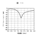
この構成における送信時の送受信間アイソレーションの周波数依存性を図11に示す。例えば、20dBのアイソレーションが得られる周波数範囲は2.0±0.2GHzにとどまり、狭帯域である他、アイソレーションの最大値も23dB程度で低い。 FIG. 11 shows the frequency dependence of isolation between transmission and reception during transmission in this configuration. For example, the frequency range in which isolation of 20 dB can be obtained is only 2.0 ± 0.2 GHz, and in addition to a narrow band, the maximum value of isolation is as low as about 23 dB.
次に、非特許文献1に開示された回路の一部を図12に示す。同図の回路は、アンテナ端子111と送信端子112及び受信端子113、114、115との接続切替を高耐圧スイッチ116で切替えるアンテナスイッチ回路である。高出力信号の送信時、送信端子112に接続されたスイッチは導通状態となる。そして、受信端子113〜115に接続されたスイッチは非導通となり、高い電圧が印加される。
Next, a part of the circuit disclosed in
このスイッチ回路の耐圧は、スイッチとして用いるトランジスタの空乏層容量の耐圧で決まるため、耐圧確保のためにトランジスタの多段接続が必要になる。非特許文献1の場合、高耐圧スイッチ116は、図13のようにシングルゲート構成によりi、j間で4段の接続が必要となっている。
Since the withstand voltage of this switch circuit is determined by the withstand voltage of the depletion layer capacitance of the transistor used as a switch, it is necessary to connect the transistors in multiple stages to ensure the withstand voltage. In the case of Non-Patent
図10に示したアンテナスイッチ回路を1個の送信回路と2個の受信回路と1個のアンテナとの接続を切替えるアンテナスイッチ回路に拡張して構成すると、図14に示すようになる。アイソレーション特性が狭帯域であるため、受信端子109とアンテナ端子104との間に、回路の動作周波数の種類毎に実効波長の1/4に相当する伝送回路108とスイッチ110が更に必要になる。動作周波数の種類が増えるに伴って追加する伝送回路が増え、アンテナスイッチ回路の構成が複雑になる。
If the antenna switch circuit shown in FIG. 10 is extended to an antenna switch circuit that switches connection between one transmission circuit, two reception circuits, and one antenna, the configuration is as shown in FIG. Since the isolation characteristic is a narrow band, a
また、図12に示した回路でも受信回路毎にスイッチが必要になり、受信回路が増えるに伴って追加する高耐圧スイッチが増え、アンテナスイッチ回路の構成が複雑になる。更に、高耐圧スイッチには、多段接続において挿入損失の増大を防ぐために、ゲート幅が大きいトランジスタが必要となる。そのため、素子面積が増大し、チップ面積が増大する。 In addition, the circuit shown in FIG. 12 also requires a switch for each receiving circuit. As the number of receiving circuits increases, the number of high voltage switches to be added increases, and the configuration of the antenna switch circuit becomes complicated. Further, a high breakdown voltage switch requires a transistor having a large gate width in order to prevent an increase in insertion loss in a multistage connection. Therefore, the element area increases and the chip area increases.
本発明の主たる目的は、構成が簡単で、かつ送受信間で高いアイソレーションが得られるアンテナスイッチ回路を提供することにある。 A main object of the present invention is to provide an antenna switch circuit that has a simple configuration and can provide high isolation between transmission and reception.
また、その付加的な目的は、スイッチの素子面積の増加を防ぐことができるアンテナスイッチ回路を提供することにある。 An additional object of the present invention is to provide an antenna switch circuit that can prevent an increase in the element area of the switch.
上記主たる目的を達成するための本発明のアンテナスイッチ回路は、送信信号を入力する送信端子及び受信信号を出力する複数の受信端子のいずれかにアンテナ端子を接続するためのアンテナスイッチ回路であって、上記送信端子と上記アンテナ端子との間に接続した第1のスイッチと、一端を上記アンテナ端子に接続した、使用する周波数において送信信号の位相を90°回転させる伝送回路と、一端が上記伝送回路の他端に接続され、他端が接地された第2のスイッチと、上記伝送回路の他端と上記複数の受信端子の各々との間に接続した第3のスイッチとを具備することを特徴とする。 An antenna switch circuit of the present invention for achieving the main object is an antenna switch circuit for connecting an antenna terminal to any one of a transmission terminal for inputting a transmission signal and a plurality of reception terminals for outputting a reception signal. A first switch connected between the transmission terminal and the antenna terminal, a transmission circuit having one end connected to the antenna terminal and rotating the phase of the transmission signal by 90 ° at a frequency to be used, and one end transmitting the signal A second switch connected to the other end of the circuit and grounded at the other end; and a third switch connected between the other end of the transmission circuit and each of the plurality of receiving terminals. Features.
上記伝送回路を複数の受信端子で共通に使用するので、構成が簡単になり、更に送受信間のアイソレーションが上記伝送回路と上記第2のスイッチの組合せ及び第3のスイッチによって2段階で行なわれるので高いアイソレーションを得ることができる。 Since the transmission circuit is shared by a plurality of receiving terminals, the configuration is simplified, and further, the isolation between transmission and reception is performed in two stages by the combination of the transmission circuit and the second switch and the third switch. Therefore, high isolation can be obtained.
上記付加的な目的を達成するための本発明のアンテナスイッチ回路は、送信信号を入力する送信端子及び受信信号を出力する複数の受信端子のいずれかにアンテナ端子を接続するためのアンテナスイッチ回路であって、上記送信端子と上記アンテナ端子との間に接続した第1のスイッチと、一端が上記アンテナ端子に接続された第2のスイッチと、上記第2のスイッチの他端と上記複数の受信端子の各々との間に接続した第3のスイッチとを具備することを特徴とする。 An antenna switch circuit of the present invention for achieving the additional object is an antenna switch circuit for connecting an antenna terminal to any one of a transmission terminal for inputting a transmission signal and a plurality of reception terminals for outputting a reception signal. A first switch connected between the transmission terminal and the antenna terminal; a second switch having one end connected to the antenna terminal; the other end of the second switch; and the plurality of receptions. And a third switch connected between each of the terminals.
上記第2のスイッチを複数の受信端子で共通に使用するので、構成が簡単になり、更に送受信間のアイソレーションが上記第2のスイッチ及び第3のスイッチの2段階で行なわれるので高いアイソレーションを得ることができる他、第3のスイッチは、第2のスイッチよりも耐圧を低くしてよいため、スイッチの素子面積が受信端子が増えるに伴って増加するのを抑えることができる。 Since the second switch is used in common by a plurality of receiving terminals, the configuration is simplified, and the isolation between transmission and reception is performed in two stages, the second switch and the third switch, so that high isolation is achieved. In addition, since the third switch may have a lower withstand voltage than the second switch, an increase in the element area of the switch as the number of reception terminals increases can be suppressed.
本発明によれば、複数の送受信端子とアンテナ端子との接続を切替えるアンテナスイッチ回路において、広い周波数帯域に亘って高アイソレーション及び低損失を実現することができる。 According to the present invention, high isolation and low loss can be realized over a wide frequency band in an antenna switch circuit that switches connections between a plurality of transmission / reception terminals and antenna terminals.
以下、本発明に係るアンテナスイッチ回路を図面に示した実施形態を参照して更に詳細に説明する。なお、図1、図3〜図5及び図9における同一の符号は、同一物又は類似物を表示するものとし、説明の重複を避ける。 Hereinafter, the antenna switch circuit according to the present invention will be described in more detail with reference to embodiments shown in the drawings. In addition, the same code | symbol in FIG.1, FIG.3-FIG.5 and FIG.9 shall display the same thing or a similar thing, and avoids duplication of description.
本発明の第1の実施形態を図1を用いて説明する。同図に、高出力の送信信号を扱う1個の送信回路1及び2個の受信回路2、3と1個のアンテナ端子4との接続を切替えるアンテナスイッチ回路を示す。
A first embodiment of the present invention will be described with reference to FIG. The figure shows an antenna switch circuit for switching the connection between one
送信回路1の出力信号を入力する送信端子31とアンテナ端子4の間に1入力1出力のスイッチ素子5が接続される。また、アンテナ端子4に伝送回路9の一端が接続され、伝送回路9の他端に1入力1出力のスイッチ6の一端が接続される。スイッチ6の他端は接地される。伝送回路9の長さは実効波長の1/4である。伝送回路9は、使用する周波数において送信信号の位相を90度回転させる。受信回路2、3に受信信号を与える受信端子32、33とスイッチ6の一端の間に1入力1出力のスイッチ7、8がそれぞれ接続される。
A
スイッチ5〜8は、HEMT(High Electron Mobility Transistor)素子で構成される。端子14〜17は、それぞれスイッチ5〜8の導通状態、非導通状態を制御するコントロール端子である。また、抵抗素子10〜13は、端子14〜17をそれぞれスイッチ5〜8から高周波的に分離するために用いられる。
The
送信時、スイッチ5、6は導通状態となり、スイッチ7、8は非導通状態となる。このとき、アンテナ端子4とスイッチ5と伝送回路9との接続点aから、スイッチ6と伝送回路9の接続点bをみたインピーダンスは、接続点bがスイッチ6を介して低インピーダンスで接地され、かつ伝送回路の位相が90度回転しているため、高くなっている。
At the time of transmission, the
接続点aと接続点bの間のアイソレーションの量は、スイッチ6の導通状態のインピーダンスで決まる。本実施形態ではHEMT素子を使っているため、他の電界効果型トランジスタであるJFET(junction Field Effect Transistor)素子やMESFET(Metal Semiconductor Field Effect Transistor)素子に比べて高いアイソレーションを実現することができる。
The amount of isolation between the connection point a and the connection point b is determined by the impedance of the
次に、接続点aと受信回路2、3との間には、接続点aと接続点bの間の上記のアイソレーションに、非導通のスイッチ7、8によるアイソレーションが加わる。非導通のスイッチ7、8が容量性のため、周波数が低くなるほど高いアイソレーションが得られる。
Next, isolation between the connection point a and the
このようにして得られた本実施形態のアイソレーション特性を図2に示す。2.7GHz以下の広い帯域で20dBのアイソレーションが得られている。即ち、本実施形態においては、接続点aと受信回路2及び受信回路3との間のアイソレーションは、伝送回路9とスイッチ6とのアイソレーション及びスイッチ7、8のアイソレーションの双方により、広い周波数帯域に亘って高いアイソレーションを実現することができる。従って、接続点aから受信回路2、3への信号漏洩は小さくなり、送信回路1から出力された高出力の送信信号は、低損失でアンテナ端子4へ伝送される。
FIG. 2 shows the isolation characteristics of the present embodiment thus obtained. Isolation of 20 dB is obtained in a wide band of 2.7 GHz or less. That is, in this embodiment, the isolation between the connection point a and the receiving
また、スイッチ5、6は、送信時に導通状態になるため耐圧を要求されない。スイッチ7、8についても、伝送回路9とスイッチ6とのアイソレーションにより送信信号が十分に減衰するため耐圧は要求されない。また、送信信号が十分に減衰することから、スイッチ7、8は、送信信号に対して損失、歪の影響を及ぼさない。即ち、送信信号に対して低損失、低歪みのスイッチが提供されることになる。
Further, since the
続いて、受信時の動作を、受信回路2で受信する場合を採り上げて説明する。スイッチ5、6は非導通状態となり、スイッチ7は導通状態、スイッチ8は非導通状態となる。アンテナ端子4から受信された信号は、伝送回路9、スイッチ7を経て受信回路2に伝送される。スイッチ5とスイッチ8が非導通状態のため、送信回路1と受信回路3へは伝送されない。また、受信信号は微弱であるため、歪みの問題はない。
Subsequently, the operation at the time of reception will be described by taking the case of reception by the
なお、送信周波数が同じ場合には伝送回路を共通に用いることができるので、受信回路は本実施形態のように2個に限らず、更に多くすることが可能である。 Note that when the transmission frequency is the same, the transmission circuit can be used in common, so the number of reception circuits is not limited to two as in the present embodiment, and can be increased.
図3に本発明の第2の実施形態を示す。本実施形態では、送信時の送受信間のアイソレーションと受信間のアイソレーションを更に向上させるために、スイッチ7と受信回路2の間に、一端が接地されたスイッチ18が接続され、更に、スイッチ8と受信回路3の間に、一端が接地されたスイッチ21が接続される。スイッチ18、21は、HEMT素子で構成される。
FIG. 3 shows a second embodiment of the present invention. In the present embodiment, in order to further improve the isolation between transmission and reception during transmission and the isolation between reception, a
端子20、23は、それぞれスイッチ18、21の導通状態と非導通状態を制御するコントロール端子である。抵抗素子19、22は、端子20、23とHEMTスイッチ18、21とをそれぞれ高周波的に分離するために用いられる。
送信時にスイッチ18、21を導通状態にすることにより、送信時のアイソレーションが向上する。また、受信時に受信する回路に接続されているスイッチを非導通状態にし、更に、受信しない回路に接続されているスイッチを導通状態にして受信しない回路を接地することにより、受信回路間のアイソレーションが向上する。
By making the
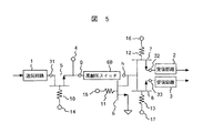
図4に本発明の第3の実施形態を示す。本実施形態は、携帯電話の複数の通信規格に対応するように構成したアンテナスイッチ回路であり、現行の通信規格であるGSM(Global System for Mobile communications)とPCS(Personal Communication Services)とDCS(Digital Communication System)の接続切替が可能である。GSMは送信1系統に対し受信が2系統となり、PCS及びDCSは送信回路を共通にすることによって両者で送信1系統、受信がPCSで1系統、DCSで1系統となる。 FIG. 4 shows a third embodiment of the present invention. The present embodiment is an antenna switch circuit configured to correspond to a plurality of communication standards for mobile phones, and is a current communication standard such as GSM (Global System for Mobile communications), PCS (Personal Communication Services), and DCS (Digital Communication System) connection switching is possible. GSM has two systems for reception with respect to one transmission system, and PCS and DCS have one transmission system by using a common transmission circuit, one system for reception by PCS, and one system by DCS.
GSMは900MHz帯、PCSとDCSは1800MHz帯であるため、位相が90度回転する伝送回路の長さの差が大きい。そのため、GSMとPCS及びDCSとは、アンテナ端子4とGSM端子27とPCS/DCS端子44を持つ分波器58を使って分離される。その上で、GSM端子27、PCS/DCS端子44にはそれぞれ図1のスイッチ回路が接続される。
Since GSM is in the 900 MHz band and PCS and DCS are in the 1800 MHz band, there is a large difference in the length of the transmission circuit whose phase rotates 90 degrees. Therefore, GSM, PCS and DCS are separated by using a
即ち、本実施形態は、アンテナ端子4と送信端子31a及び受信端子32a、33a、並びに送信端子31b及び受信端子32b、33bとの間に構成したアンテナスイッチ回路である。なお、GSM端子27、PCS/DCS端子44をそれぞれ副アンテナ端子と云い、GSM側の図1のスイッチ回路及びPCS/DCS側の図1のスイッチ回路をそれぞれ副アンテナスイッチ回路と云うこととする。それぞれの副アンテナスイッチ回路における符号には、図1の符号に添え字a、bを付記したものが用いられる。
That is, this embodiment is an antenna switch circuit configured between the
また、伝送回路9aの長さは、GSMの送信側周波数において送信信号の位相が90度回転する長さに設定され、伝送回路9bの長さはPCS/DCSの送信周波数において送信信号の位相が90度回転する長さに設定される。 The length of the transmission circuit 9a is set so that the phase of the transmission signal is rotated 90 degrees at the GSM transmission side frequency, and the length of the transmission circuit 9b is the transmission signal phase at the PCS / DCS transmission frequency. The length is set to rotate 90 degrees.
GSM送信時、スイッチ5a、6aは導通状態、スイッチ7a、8aは非導通状態となる。このとき、伝送回路9aとスイッチ6aにより、接続点cからみた接続点dは高インピーダンスとなり、更に接続点dからみた受信回路2a、3aも高インピーダンスになる。それにより、広い周波数帯域に亘って送受信間で高いアイソレーションが実現される。このため、送信回路1aから出力された高出力の送信信号は、受信回路へ殆ど漏洩することなく、スイッチ5a、端子27、分波器58を経てアンテナ端子4へ伝送される。
During GSM transmission, the
高出力の送信信号は最大4Wに達するが、スイッチ5a、6aが導通状態となっているため、スイッチ5a、6aに印加される電圧は1Vにも満たない程度である。非導通状態のスイッチ7a、8aも同程度の電圧しか印加されないので、送信信号に与える歪みの影響は少ない。
A high-power transmission signal reaches 4 W at the maximum, but since the
続いて、GSM受信時の動作について、受信回路2aが受信を行なう場合を例にとって説明する。スイッチ5a、6a、8aは非導通状態、スイッチ7aは導通状態となるため、アンテナ端子4から入力されたGSM受信信号は、分波器58を経て端子27に出力され、スイッチ7aを経て受信回路2aへ伝送される。受信信号の強度は微弱であるため、受信信号に与える歪みの問題はない。なお、受信回路3aが受信を行なう場合は、スイッチ5a、6a、7aが非導通状態、スイッチ8aが導通状態となる。
Next, the operation at the time of GSM reception will be described taking as an example the case where the
次に、PCS/DCS送信時、スイッチ5b、6bは導通状態、スイッチ7b、8bは非導通状態となる。このとき、伝送回路9bとスイッチ6bにより、接続点eからみた接続点fは高インピーダンスとなり、更に接続点fからみた受信回路2b、3bも高インピーダンスになっているため、広い周波数帯域に亘って送受信間で高いアイソレーションが実現される。このため、送信回路1bから出力された高出力の送信信号は、受信回路へ漏洩することなくスイッチ5b、端子44、分波器58を経てアンテナ端子4へ伝送される。高出力の送信信号は、最大2〜3Wに達するが、スイッチ5b、6bが導通状態となっているためスイッチ5b、6bに印加される電圧は1Vにも満たない程度である。非導通状態のスイッチ7b、8bも同程度の電圧しか印加されないので、送信信号に与える歪みの影響は少ない。
Next, at the time of PCS / DCS transmission, the
PCS受信時、スイッチ5b、6b、8bは非導通状態、スイッチ7bは導通状態となるため、アンテナ端子4から入力されたPCS受信信号は、分波器58を経て端子44に出力され、スイッチ7bを経て受信回路2bへ伝送される。受信信号の強度は微弱であるため、受信信号に与える歪みの問題はない。
When receiving the PCS, the
DCS受信時、スイッチ5b、6b、7bが非導通状態、スイッチ8bが導通状態となり受信回路3bへ伝送される。
At the time of DCS reception, the
端子14a〜17a、14b〜17bはスイッチの導通状態、非導通状態を制御するコントロール端子であり、抵抗素子10a〜13a、10b〜13bは各コントロール端子とそれぞれのスイッチを高周波的に分離するために用いられる。
本実施形態により、複数の通信規格に対応しつつ、広い周波数帯域に亘って送受信間及び受信間で高アイソレーションを保ち、アンテナと各回路の間が低損失であるアンテナスイッチ回路を実現することができた。 According to the present embodiment, it is possible to realize an antenna switch circuit that supports a plurality of communication standards, maintains high isolation between transmission / reception and reception over a wide frequency band, and has low loss between the antenna and each circuit. I was able to.
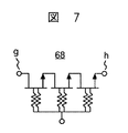
図5に本発明の第4の実施形態を示す。本実施形態においては、伝送回路に代わってスイッチ68が用いられる。本実施形態は、高出力の送信信号を扱う1個の送信回路1と2個の受信回路2、3と1個のアンテナ端子4の接続を、伝送回路を使わずに切替えるアンテナスイッチ回路である。スイッチ5、7、8はHEMTで構成される。
FIG. 5 shows a fourth embodiment of the present invention. In this embodiment, a
送信時、スイッチ5は導通状態、スイッチ7、8、68は非導通状態となる。スイッチ68は、送信回路1から出力される高出力の送信信号をアンテナ端子4へ低損失、低歪みで伝送させるために、非導通状態で十分な耐圧が要求される。アンテナ端子4における送信出力信号は最大4Wに達し、高耐圧スイッチ68には27V前後の電圧が印加される。
At the time of transmission, the
この電圧に対して耐圧を確保するスイッチ素子として、高耐圧スイッチ68に多段接続のHEMTが用いられる。ピンチオフ電圧を−0.5〜−1.0Vにし、制御電圧を−2.8Vにした場合の高耐圧スイッチ68は、図6のようにシングルゲート構成で4〜6段、図7のようにデュアルゲート構成では2段〜3段、図8のようにトリプルゲート構成では2段の接続が必要となる。
A multi-stage HEMT is used for the high
スイッチ68のアイソレーションにより、送信信号の電力が十分に減衰されるためスイッチ7、8は、シングルゲートによって構成することができる。なお、スイッチ68のアイソレーションを補うことが必要になる場合には、高耐圧スイッチ68とスイッチ7、8との接続部分に一端が接地されたスイッチ6が接続される。スイッチ6をスイッチ5と同じ動作状態にすることによってアイソレーションが一層向上し、スイッチ7、8の歪みを更に緩和することができる。スイッチ6もHEMTで構成される。
Since the power of the transmission signal is sufficiently attenuated by the isolation of the
本実施形態によって、従来は受信回路毎に必要であった高耐圧スイッチを共通の高耐圧スイッチ68のみとすることができ、スイッチの素子面積の増加を防ぐことができた。
According to the present embodiment, the common
図9に本発明の第5の実施形態を示す。本実施形態は、携帯電話のGSMとPCSとDCSの接続切替を可能とするアンテナスイッチ回路である。GSMは送信1系統に対し受信が2系統、PCS/DCSは送信回路を共通にすることができるため送信が1系統で受信がPCSで1系統、DCSで1系統となる。 FIG. 9 shows a fifth embodiment of the present invention. This embodiment is an antenna switch circuit that enables connection switching between GSM, PCS, and DCS of a mobile phone. GSM can receive two lines for one transmission line, and PCS / DCS can share a transmission circuit. Therefore, transmission is one line, reception is one line for PCS, and one line is for DCS.
アンテナ端子4と送信回路1aに接続する送信端子31aとの間、及びアンテナ端子4と送信回路1bに接続する送信端子31bとの間にそれぞれ高耐圧スイッチ83、84が接続され、アンテナ端子4に高耐圧スイッチ68が接続される。更に、高耐圧スイッチ68と受信回路78〜81の間にそれぞれスイッチ87〜90が接続される。端子96〜99はスイッチ87〜90の導通状態、非導通状態を制御するコントロール端子であり、抵抗素子92〜95は各コントロール端子とそれぞれのスイッチとを高周波的に分離するために用いられる。
High voltage switches 83 and 84 are connected between the
スイッチ83、84、68には、GSMの場合に最大出力電力が4Wに達するときでも歪みが発生しないように、それぞれ図6、図7又は図8に示した高耐圧スイッチが使用される。なお、高耐圧スイッチ68に対してアイソレーションを補うことが必要になる場合に、スイッチ6が設けられる。
As the
GSM送信時、スイッチ83、6は導通状態、スイッチ84、68、87〜90は非導通状態となる。送信回路1aから出力された高出力の送信信号は、アンテナ端子4へ伝送される。
During GSM transmission, the
PCS/DCS送信時、スイッチ84、6は導通状態、スイッチ83、68、87〜90は非道通状態となる。 送信回路1bから出力された高出力の送信信号はアンテナ端子4へ伝送される。
During PCS / DCS transmission, the
受信時、スイッチ83、84、6は非導通状態、スイッチ68は導通状態となる。スイッチ87〜90のうち、受信する受信回路に接続されたスイッチのみが導通状態となり、他は非導通状態となる。従って、アンテナ端子4から入力された受信信号は、導通状態となったスイッチを経て受信回路に伝送される。端子96〜99はスイッチ87〜90の導通状態、非導通状態を制御するコントロール端子であり、抵抗素子92〜95は各コントロール端子とそれぞれのスイッチを高周波的に分離するために用いられる。
At the time of reception, the
本実施形態により、複数の通信規格に対応しつつ、スイッチの素子面積の増加を防ぐことができた。 According to this embodiment, an increase in the element area of the switch can be prevented while supporting a plurality of communication standards.
図15に本発明の第6の実施形態を示す。本実施形態は、第5の実施形態のアンテナスイッチ回路を用いて構成した高周波モジュールであり、携帯電話のGSMとPCSとDCSに対応する。GSMは送信1系統に対して受信が2系統(GSM_1、GSM_2)、PCS/DCSは送信回路を共通にすることができるため送信が1系統で受信がPCSで1系統、DCSで1系統となる。 FIG. 15 shows a sixth embodiment of the present invention. The present embodiment is a high-frequency module configured using the antenna switch circuit of the fifth embodiment, and corresponds to GSM, PCS, and DCS of mobile phones. GSM can receive two systems (GSM_1, GSM_2) with respect to one transmission system, and PCS / DCS can have a common transmission circuit, so transmission is one system, reception is one system with PCS, and one system with DCS. .
本実施形態の高周波モジュール111には、GSM用の電力増幅回路112、GSM用の電力増幅回路112の高調波を除去するローパスフィルタ113、PCS/DCS用の電力増幅回路114、PCS/DCS用の電力増幅回路114の高調波を除去するローパスフィルタ115、本発明の第5の実施形態で示したアンテナスイッチ回路116、電力増幅回路112、114の出力電力の制御及びスイッチ回路116の接続切替えを制御する制御回路117、スイッチの各受信端子に接続された受信信号に対して妨害になる雑音を除去するSAWフィルタ118、134、135、136と受信回路119が搭載される。また、高周波モジュール111は、アンテナ端子121、GSM用変調信号端子122、PCS/DCS用変調信号端子123、制御回路にバイアス、制御信号を入力するための端子124、復調信号端子125を有している。
The high-
スイッチ回路116は図9と同等のスイッチ回路で、その高耐圧スイッチ部のスイッチ126、127、128の各々はデュアルゲート3段で構成されるが、図6のようなシングルゲート6段、図8のようなトリプルゲート2段で構成されてもよい。集積化した本回路のチップサイズは約1mm2である。
The
本実施形態の動作をPCS送受信時の場合を例にとって説明する。PCS受信時、電力増幅回路112、114は非動作状態、スイッチ126、127、129、130、132、133は非導通状態、スイッチ128、131は導通状態となるため、端子121から入力された受信信号はスイッチ128、131、SAWフィルタ135を経て受信回路119に入力されて復調され、端子125に出力される。
The operation of this embodiment will be described by taking the case of PCS transmission / reception as an example. When receiving the PCS, the
次にPCS送信時においては、PCS送信周波数とDCS受信周波数のうち1850MHzから1875MHzは動作周波数が重なっているため、この帯域のPCSの送信信号が出力された場合、SAWフィルタ136に入力される電力はPCS送信とDCS受信間のアイソレーションによって決まる。もし、アイソレーションが不足すると、SAWフィルタ136はPCSの送信信号の電力が過入力になるためSAWフィルタ136の破壊、更には受信回路119の破壊を招くこととなる。本実施形態では、スイッチ128、132、133によって高いアイソレーションが得られるため、そのような破壊が回避される。
Next, at the time of PCS transmission, since the operating frequency overlaps between 1850 MHz and 1875 MHz among the PCS transmission frequency and the DCS reception frequency, the power input to the
PCS送信時、制御回路117によりGSM用電力増幅回路112が非動作状態、スイッチ126、128、129、130、131、132が非導通状態、PCS/DCS用電力増幅回路114が動作状態、スイッチ127、133が導通状態となる。端子123に入力された信号は、PCS/DCS用電力増幅回路114で増幅され、スイッチ127を経て端子121に出力される。このとき、スイッチ128、129、130、131、132は非導通状態、スイッチ133は導通状態となっているため、高いアイソレーションを広い周波数帯域で得ることができる。従って、受信側のSAWフィルタ136、受信回路119が破壊されるのを防ぐことができる。
At the time of PCS transmission, the
なお、高耐圧スイッチは、スイッチに接続される高周波伝送路の長さがスイッチの動作周波数の伝送路内波長の1/10以下である場合、スイッチに1Wを超えるような高周波電力を入力したとき、その高周波伝送路の長さが変化してもオフ状態を保ち続けることができるスイッチである必要がある。そのため、本実施形態では、スイッチ126、127、128にシングルゲートの多段接続やデュアルゲート、トリプルゲートなどのマルチゲート単体又はその多段接続したものが用いられる。シングルゲート1段のスイッチは、それだけでオフ状態を保ち続けることができる電力は1W未満であるため高耐圧スイッチとして用いることができない。
When the length of the high-frequency transmission line connected to the switch is 1/10 or less of the wavelength within the transmission line of the operating frequency of the switch, the high-voltage switch is used when high-frequency power exceeding 1 W is input to the switch. The switch needs to be able to keep the off state even if the length of the high-frequency transmission line changes. Therefore, in the present embodiment, a single gate multistage connection or a multigate single body such as a dual gate or a triple gate or a multistage connection thereof is used for the
本発明のアンテナスイッチ回路を送受信を行なう高周波モジュールに適用することにより、スイッチの高耐圧特性により高い送信電力を扱うことが可能となり、更に高耐圧スイッチとモード切替スイッチの直列接続により送受信間で高アイソレーションが実現できるため、デュプレクサなどの大型な受動部品が不要になると共に、モジュールの薄層化、小型化が可能な高周波モジュールを実現することができる。 By applying the antenna switch circuit of the present invention to a high-frequency module that performs transmission / reception, it is possible to handle high transmission power due to the high breakdown voltage characteristics of the switch, and further, high transmission / reception can be achieved between the transmission and reception by serial connection of the high breakdown voltage switch and the mode switch. Since isolation can be realized, a large passive component such as a duplexer is not required, and a high-frequency module that can be thinned and downsized can be realized.
1…送信回路、2,3…受信回路、5〜8…スイッチ、9…位相を90度回転させる伝送回路、10〜13…抵抗素子、14〜17…制御端子、4…アンテナ端子、68…高耐圧スイッチ、31…送信端子、32,33…受信端子。
DESCRIPTION OF
Claims (18)
上記送信端子と上記アンテナ端子との間に接続された第1のスイッチと、
一端が上記アンテナ端子に接続され、使用する周波数において位相を所望の値回転させられた送信信号が他端から得られる伝送回路と、
一端が上記伝送回路の上記他端に接続され、他端が交流的に接地された第2のスイッチと、
上記伝送回路の上記他端と上記複数の受信端子の各々との間に接続された複数の第3のスイッチとを具備することを特徴とするアンテナスイッチ回路。 An antenna switch circuit for selecting any of a transmission terminal to which a transmission signal is input and a plurality of reception terminals to which a reception signal is output and coupling it to the antenna terminal,
A first switch connected between the transmission terminal and the antenna terminal;
A transmission circuit in which one end is connected to the antenna terminal and a transmission signal whose phase is rotated by a desired value at a frequency to be used is obtained from the other end;
A second switch having one end connected to the other end of the transmission circuit and the other end grounded in an alternating manner;
An antenna switch circuit comprising: a plurality of third switches connected between the other end of the transmission circuit and each of the plurality of reception terminals.
アンテナ端子と2個の上記副アンテナ端子との間に接続された分波器とを具備し、
上記副アンテナスイッチ回路は、
上記送信端子と上記副アンテナ端子との間に接続された第1のスイッチと、
一端が上記副アンテナ端子に接続され、使用する周波数において位相を所望の値回転させられた送信信号が他端から得られる伝送回路と、
一端が上記伝送回路の上記他端に接続され、他端が交流的に接地された第2のスイッチと、
上記伝送回路の上記他端と上記複数の受信端子の各々との間に接続された複数の第3のスイッチとを具備することを特徴とするアンテナスイッチ回路。 Two sub-antenna switch circuits for selecting one of a plurality of receiving terminals from which a transmission signal is input and a plurality of receiving terminals from which a reception signal is output and coupling to the sub-antenna terminal;
A duplexer connected between the antenna terminal and the two auxiliary antenna terminals,
The sub antenna switch circuit is
A first switch connected between the transmission terminal and the sub-antenna terminal;
A transmission circuit in which one end is connected to the sub-antenna terminal and a transmission signal whose phase is rotated by a desired value at a frequency to be used is obtained from the other end;
A second switch having one end connected to the other end of the transmission circuit and the other end grounded in an alternating manner;
An antenna switch circuit comprising: a plurality of third switches connected between the other end of the transmission circuit and each of the plurality of reception terminals.
上記送信端子と上記アンテナ端子との間に接続された第1のスイッチと、
一端が上記アンテナ端子に接続され、上記複数の受信端子のいずれかが選択されて他端に結合される第2のスイッチと、
上記第2のスイッチの上記他端と上記複数の受信端子の各々との間の結合経路に接続された複数の第3のスイッチとを具備することを特徴とするアンテナスイッチ回路。 An antenna switch circuit for selecting one of a plurality of receiving terminals from which a transmission signal is input and a plurality of receiving terminals from which a reception signal is output, and connecting the antenna terminal to the antenna terminal,
A first switch connected between the transmission terminal and the antenna terminal;
A second switch having one end connected to the antenna terminal and one of the plurality of receiving terminals selected and coupled to the other end;
An antenna switch circuit comprising: a plurality of third switches connected to a coupling path between the other end of the second switch and each of the plurality of reception terminals.
送信回路及び受信回路の少なくとも一方とを具備して成り、
上記アンテナスイッチ回路は、
送信信号が入力される送信端子及び受信信号が出力される複数の受信端子のいずれかを選択してアンテナ端子に接続するためのアンテナスイッチ回路であって、
上記送信端子と上記アンテナ端子との間に接続された第1のスイッチと、
一端が上記アンテナ端子に接続され、上記複数の受信端子のいずれかが選択されて他端に結合される第2のスイッチと、
上記第2のスイッチの上記他端と上記複数の受信端子の各々との間の結合経路に接続された複数の第3のスイッチとを具備することを特徴とする高周波モジュール。 An antenna switch circuit;
Comprising at least one of a transmission circuit and a reception circuit,
The antenna switch circuit is
An antenna switch circuit for selecting one of a plurality of receiving terminals from which a transmission signal is input and a plurality of receiving terminals from which a reception signal is output, and connecting the antenna terminal to the antenna terminal,
A first switch connected between the transmission terminal and the antenna terminal;
A second switch having one end connected to the antenna terminal and one of the plurality of receiving terminals selected and coupled to the other end;
A high-frequency module comprising: a plurality of third switches connected to a coupling path between the other end of the second switch and each of the plurality of reception terminals.
Priority Applications (3)
| Application Number | Priority Date | Filing Date | Title |
|---|---|---|---|
| JP2004189257A JP2005136948A (en) | 2003-10-08 | 2004-06-28 | Antenna switch circuit |
| US10/921,815 US20050079829A1 (en) | 2003-10-08 | 2004-08-20 | Antenna switch |
| CN200410057564.5A CN1606248A (en) | 2003-10-08 | 2004-08-20 | Antenna switch circuit |
Applications Claiming Priority (2)
| Application Number | Priority Date | Filing Date | Title |
|---|---|---|---|
| JP2003348990 | 2003-10-08 | ||
| JP2004189257A JP2005136948A (en) | 2003-10-08 | 2004-06-28 | Antenna switch circuit |
Publications (2)
| Publication Number | Publication Date |
|---|---|
| JP2005136948A true JP2005136948A (en) | 2005-05-26 |
| JP2005136948A5 JP2005136948A5 (en) | 2007-04-12 |
Family
ID=34425367
Family Applications (1)
| Application Number | Title | Priority Date | Filing Date |
|---|---|---|---|
| JP2004189257A Withdrawn JP2005136948A (en) | 2003-10-08 | 2004-06-28 | Antenna switch circuit |
Country Status (3)
| Country | Link |
|---|---|
| US (1) | US20050079829A1 (en) |
| JP (1) | JP2005136948A (en) |
| CN (1) | CN1606248A (en) |
Cited By (6)
| Publication number | Priority date | Publication date | Assignee | Title |
|---|---|---|---|---|
| US7847655B2 (en) | 2007-07-31 | 2010-12-07 | Samsung Electro-Mechanics., Ltd. | Switching circuit |
| JP2011097557A (en) * | 2009-05-26 | 2011-05-12 | Murata Mfg Co Ltd | High-frequency switch module |
| JP2012054635A (en) * | 2010-08-31 | 2012-03-15 | Hitachi Metals Ltd | High frequency circuit, high frequency component, and communication device |
| JP2015008493A (en) * | 2009-05-26 | 2015-01-15 | 株式会社村田製作所 | High-frequency switch module |
| KR20150042808A (en) * | 2012-08-09 | 2015-04-21 | 퀄컴 인코포레이티드 | Multi-throw antenna switch with off-state capacitance reduction |
| WO2017083596A1 (en) * | 2015-11-13 | 2017-05-18 | Skyworks Solutions, Inc. | Integrated switch-filter network |
Families Citing this family (30)
| Publication number | Priority date | Publication date | Assignee | Title |
|---|---|---|---|---|
| US6804502B2 (en) | 2001-10-10 | 2004-10-12 | Peregrine Semiconductor Corporation | Switch circuit and method of switching radio frequency signals |
| EP1774620B1 (en) | 2004-06-23 | 2014-10-01 | Peregrine Semiconductor Corporation | Integrated rf front end |
| US7400862B2 (en) * | 2004-10-25 | 2008-07-15 | Skyworks Solutions, Inc. | Transmit-receive switch architecture providing pre-transmit isolation |
| US20080076371A1 (en) | 2005-07-11 | 2008-03-27 | Alexander Dribinsky | Circuit and method for controlling charge injection in radio frequency switches |
| US7910993B2 (en) | 2005-07-11 | 2011-03-22 | Peregrine Semiconductor Corporation | Method and apparatus for use in improving linearity of MOSFET's using an accumulated charge sink |
| US7890891B2 (en) | 2005-07-11 | 2011-02-15 | Peregrine Semiconductor Corporation | Method and apparatus improving gate oxide reliability by controlling accumulated charge |
| USRE48965E1 (en) | 2005-07-11 | 2022-03-08 | Psemi Corporation | Method and apparatus improving gate oxide reliability by controlling accumulated charge |
| US8742502B2 (en) | 2005-07-11 | 2014-06-03 | Peregrine Semiconductor Corporation | Method and apparatus for use in improving linearity of MOSFETs using an accumulated charge sink-harmonic wrinkle reduction |
| US9653601B2 (en) | 2005-07-11 | 2017-05-16 | Peregrine Semiconductor Corporation | Method and apparatus for use in improving linearity of MOSFETs using an accumulated charge sink-harmonic wrinkle reduction |
| JP4724498B2 (en) * | 2005-08-30 | 2011-07-13 | ルネサスエレクトロニクス株式会社 | Semiconductor integrated circuit device and high frequency power amplification module |
| JP4712492B2 (en) * | 2005-08-31 | 2011-06-29 | ルネサスエレクトロニクス株式会社 | Semiconductor integrated circuit device and high frequency power amplification module |
| GB2439622B (en) * | 2006-06-28 | 2011-03-30 | Filtronic Compound Semiconductors Ltd | A linear antenna switch arm |
| JP4939125B2 (en) * | 2006-06-29 | 2012-05-23 | ルネサスエレクトロニクス株式会社 | Semiconductor integrated circuit device and high frequency module |
| US7960772B2 (en) * | 2007-04-26 | 2011-06-14 | Peregrine Semiconductor Corporation | Tuning capacitance to enhance FET stack voltage withstand |
| EP3346611B1 (en) | 2008-02-28 | 2021-09-22 | pSemi Corporation | Method and apparatus for use in digitally tuning a capacitor in an integrated circuit device |
| US8723260B1 (en) | 2009-03-12 | 2014-05-13 | Rf Micro Devices, Inc. | Semiconductor radio frequency switch with body contact |
| JP5251953B2 (en) * | 2010-09-30 | 2013-07-31 | 株式会社村田製作所 | Switch circuit, semiconductor device, and portable radio |
| US20130015501A1 (en) * | 2011-07-11 | 2013-01-17 | International Rectifier Corporation | Nested Composite Diode |
| KR20130127782A (en) * | 2012-05-15 | 2013-11-25 | 삼성전기주식회사 | A switching circuit and a wireless communication system including the same |
| US9590674B2 (en) | 2012-12-14 | 2017-03-07 | Peregrine Semiconductor Corporation | Semiconductor devices with switchable ground-body connection |
| US20150236748A1 (en) | 2013-03-14 | 2015-08-20 | Peregrine Semiconductor Corporation | Devices and Methods for Duplexer Loss Reduction |
| US9406695B2 (en) | 2013-11-20 | 2016-08-02 | Peregrine Semiconductor Corporation | Circuit and method for improving ESD tolerance and switching speed |
| US9831857B2 (en) | 2015-03-11 | 2017-11-28 | Peregrine Semiconductor Corporation | Power splitter with programmable output phase shift |
| JP6443263B2 (en) * | 2015-08-10 | 2018-12-26 | 株式会社村田製作所 | High frequency module |
| US10298187B2 (en) | 2016-08-12 | 2019-05-21 | Qualcomm Incorporated | Selective high and low power amplifier switch architecture |
| US9948281B2 (en) | 2016-09-02 | 2018-04-17 | Peregrine Semiconductor Corporation | Positive logic digitally tunable capacitor |
| US10886911B2 (en) | 2018-03-28 | 2021-01-05 | Psemi Corporation | Stacked FET switch bias ladders |
| US10505530B2 (en) | 2018-03-28 | 2019-12-10 | Psemi Corporation | Positive logic switch with selectable DC blocking circuit |
| US10236872B1 (en) | 2018-03-28 | 2019-03-19 | Psemi Corporation | AC coupling modules for bias ladders |
| US11476849B2 (en) | 2020-01-06 | 2022-10-18 | Psemi Corporation | High power positive logic switch |
Family Cites Families (17)
| Publication number | Priority date | Publication date | Assignee | Title |
|---|---|---|---|---|
| US5477184A (en) * | 1992-04-15 | 1995-12-19 | Sanyo Electric Co., Ltd. | Fet switching circuit for switching between a high power transmitting signal and a lower power receiving signal |
| JPH11239048A (en) * | 1998-02-20 | 1999-08-31 | Sony Corp | Antenna switch circuit |
| DE19842706A1 (en) * | 1998-09-17 | 2000-03-23 | Siemens Ag | Multi-band aerial switch for multi-band mobile radio telephone |
| SE518416C2 (en) * | 1998-12-22 | 2002-10-08 | Ericsson Telefon Ab L M | Antenna Switch Module |
| US6552626B2 (en) * | 2000-01-12 | 2003-04-22 | Raytheon Company | High power pin diode switch |
| EP1237222B1 (en) * | 2001-02-27 | 2006-01-18 | Telefonaktiebolaget LM Ericsson (publ) | Multiband transformation stage for a multiband r.f. switching device |
| JP3772771B2 (en) * | 2001-05-18 | 2006-05-10 | 松下電器産業株式会社 | Multiband high frequency switch |
| GB2376384B (en) * | 2001-06-08 | 2005-03-16 | Sony Uk Ltd | Antenna switch |
| WO2003065604A1 (en) * | 2002-01-31 | 2003-08-07 | Hitachi Metals, Ltd. | Switch circuit and composite high-frequency part |
| US6882829B2 (en) * | 2002-04-02 | 2005-04-19 | Texas Instruments Incorporated | Integrated circuit incorporating RF antenna switch and power amplifier |
| US6882836B2 (en) * | 2002-07-16 | 2005-04-19 | Ericsson, Inc. | GAIT antenna interface with special isolation mode |
| US6987950B2 (en) * | 2002-07-25 | 2006-01-17 | Qualcomm, Incorporated | Radio with duplexer bypass capability |
| KR20050053757A (en) * | 2002-10-14 | 2005-06-08 | 코닌클리즈케 필립스 일렉트로닉스 엔.브이. | Transmit and receive antenna switch |
| JP3902111B2 (en) * | 2002-10-21 | 2007-04-04 | 新日本無線株式会社 | Switch semiconductor integrated circuit |
| US20040259505A1 (en) * | 2003-06-19 | 2004-12-23 | Karthik Vasanth | Switch circuit especially suitable for use in wireless LAN applications |
| US7098755B2 (en) * | 2003-07-16 | 2006-08-29 | Analog Devices, Inc. | High power, high linearity and low insertion loss single pole double throw transmitter/receiver switch |
| DE102004040967B4 (en) * | 2004-08-24 | 2019-02-21 | Snaptrack, Inc. | High isolation circuit between transmit and receive paths and device with the circuit |
-
2004
- 2004-06-28 JP JP2004189257A patent/JP2005136948A/en not_active Withdrawn
- 2004-08-20 US US10/921,815 patent/US20050079829A1/en not_active Abandoned
- 2004-08-20 CN CN200410057564.5A patent/CN1606248A/en active Pending
Cited By (9)
| Publication number | Priority date | Publication date | Assignee | Title |
|---|---|---|---|---|
| US7847655B2 (en) | 2007-07-31 | 2010-12-07 | Samsung Electro-Mechanics., Ltd. | Switching circuit |
| JP2011097557A (en) * | 2009-05-26 | 2011-05-12 | Murata Mfg Co Ltd | High-frequency switch module |
| JP2015008493A (en) * | 2009-05-26 | 2015-01-15 | 株式会社村田製作所 | High-frequency switch module |
| JP2012054635A (en) * | 2010-08-31 | 2012-03-15 | Hitachi Metals Ltd | High frequency circuit, high frequency component, and communication device |
| KR20150042808A (en) * | 2012-08-09 | 2015-04-21 | 퀄컴 인코포레이티드 | Multi-throw antenna switch with off-state capacitance reduction |
| JP2015530798A (en) * | 2012-08-09 | 2015-10-15 | クゥアルコム・インコーポレイテッドQualcomm Incorporated | Multi-throw antenna switch with off-state capacitance reduction |
| KR102096331B1 (en) * | 2012-08-09 | 2020-04-02 | 퀄컴 인코포레이티드 | Multi-throw antenna switch with off-state capacitance reduction |
| WO2017083596A1 (en) * | 2015-11-13 | 2017-05-18 | Skyworks Solutions, Inc. | Integrated switch-filter network |
| US10256794B2 (en) | 2015-11-13 | 2019-04-09 | Skyworks Solutions, Inc. | Integrated switch-filter network |
Also Published As
| Publication number | Publication date |
|---|---|
| US20050079829A1 (en) | 2005-04-14 |
| CN1606248A (en) | 2005-04-13 |
Similar Documents
| Publication | Publication Date | Title |
|---|---|---|
| JP2005136948A (en) | Antenna switch circuit | |
| US7843280B2 (en) | Systems, methods, and apparatuses for high power complementary metal oxide semiconductor (CMOS) antenna switches using body switching and substrate junction diode controlling in multistacking structure | |
| US7337547B2 (en) | High frequency switching circuit device | |
| US7847655B2 (en) | Switching circuit | |
| US20050159112A1 (en) | Switch apparatus and mobile communications terminal apparatus | |
| EP1772964B1 (en) | High-frequency switch circuit | |
| US11349469B2 (en) | High power radio frequency switches with low leakage current and low insertion loss | |
| US11742847B2 (en) | RF switch with bypass topology | |
| KR20090060901A (en) | Switching circuit for millimeter wave band applications | |
| JP4811155B2 (en) | Semiconductor switch circuit and communication equipment | |
| CN112204894B (en) | Radio frequency front-end circuit and mobile device | |
| KR101931682B1 (en) | SPDT switch structure including Transmission Line Transformer(TLT) for single antenna operation | |
| US7254371B2 (en) | Multi-port multi-band RF switch | |
| JP2004172729A (en) | Switching circuit for antenna transmission/reception | |
| JP5192900B2 (en) | Switch semiconductor integrated circuit | |
| Shiba et al. | F-band bidirectional amplifier using 75-nm InP HEMTs | |
| KR20140086487A (en) | Radio frequency switch circuit | |
| JP2008017170A (en) | Semiconductor switch circuit and communication equipment | |
| KR100712712B1 (en) | Reconfigurable multiband mixer | |
| JP2006270630A (en) | Switching circuit device | |
| JP2006081073A (en) | Transmitting/receiving circuit | |
| JP2002319848A (en) | Semiconductor switch circuit and semiconductor device |
Legal Events
| Date | Code | Title | Description |
|---|---|---|---|
| A521 | Request for written amendment filed |
Free format text: JAPANESE INTERMEDIATE CODE: A523 Effective date: 20070223 |
|
| A621 | Written request for application examination |
Free format text: JAPANESE INTERMEDIATE CODE: A621 Effective date: 20070223 |
|
| RD02 | Notification of acceptance of power of attorney |
Free format text: JAPANESE INTERMEDIATE CODE: A7422 Effective date: 20070223 |
|
| A761 | Written withdrawal of application |
Free format text: JAPANESE INTERMEDIATE CODE: A761 Effective date: 20080229 |