EP1237222B1 - Multiband transformation stage for a multiband r.f. switching device - Google Patents
Multiband transformation stage for a multiband r.f. switching device Download PDFInfo
- Publication number
- EP1237222B1 EP1237222B1 EP01104812A EP01104812A EP1237222B1 EP 1237222 B1 EP1237222 B1 EP 1237222B1 EP 01104812 A EP01104812 A EP 01104812A EP 01104812 A EP01104812 A EP 01104812A EP 1237222 B1 EP1237222 B1 EP 1237222B1
- Authority
- EP
- European Patent Office
- Prior art keywords
- multiband
- signal
- port
- coupled
- switching device
- Prior art date
- Legal status (The legal status is an assumption and is not a legal conclusion. Google has not performed a legal analysis and makes no representation as to the accuracy of the status listed.)
- Expired - Lifetime
Links
- 230000009466 transformation Effects 0.000 title claims abstract description 97
- 230000005540 biological transmission Effects 0.000 claims abstract description 34
- 238000005516 engineering process Methods 0.000 claims description 9
- 238000004088 simulation Methods 0.000 description 12
- 238000002955 isolation Methods 0.000 description 9
- 238000010586 diagram Methods 0.000 description 7
- 230000008878 coupling Effects 0.000 description 6
- 238000010168 coupling process Methods 0.000 description 6
- 238000005859 coupling reaction Methods 0.000 description 6
- 229910001218 Gallium arsenide Inorganic materials 0.000 description 4
- 239000011159 matrix material Substances 0.000 description 4
- 230000002238 attenuated effect Effects 0.000 description 2
- 239000003990 capacitor Substances 0.000 description 2
- 230000009977 dual effect Effects 0.000 description 2
- 230000003071 parasitic effect Effects 0.000 description 2
- 239000000758 substrate Substances 0.000 description 2
- 230000003213 activating effect Effects 0.000 description 1
- 238000010276 construction Methods 0.000 description 1
- 230000003247 decreasing effect Effects 0.000 description 1
- 230000001419 dependent effect Effects 0.000 description 1
- 230000000694 effects Effects 0.000 description 1
- 230000002708 enhancing effect Effects 0.000 description 1
- 238000001914 filtration Methods 0.000 description 1
- 230000007274 generation of a signal involved in cell-cell signaling Effects 0.000 description 1
- 238000003780 insertion Methods 0.000 description 1
- 230000037431 insertion Effects 0.000 description 1
- 238000010295 mobile communication Methods 0.000 description 1
- 230000000644 propagated effect Effects 0.000 description 1
- 238000012358 sourcing Methods 0.000 description 1
Images


Classifications
-
- H—ELECTRICITY
- H04—ELECTRIC COMMUNICATION TECHNIQUE
- H04B—TRANSMISSION
- H04B1/00—Details of transmission systems, not covered by a single one of groups H04B3/00 - H04B13/00; Details of transmission systems not characterised by the medium used for transmission
- H04B1/005—Details of transmission systems, not covered by a single one of groups H04B3/00 - H04B13/00; Details of transmission systems not characterised by the medium used for transmission adapting radio receivers, transmitters andtransceivers for operation on two or more bands, i.e. frequency ranges
- H04B1/0053—Details of transmission systems, not covered by a single one of groups H04B3/00 - H04B13/00; Details of transmission systems not characterised by the medium used for transmission adapting radio receivers, transmitters andtransceivers for operation on two or more bands, i.e. frequency ranges with common antenna for more than one band
- H04B1/006—Details of transmission systems, not covered by a single one of groups H04B3/00 - H04B13/00; Details of transmission systems not characterised by the medium used for transmission adapting radio receivers, transmitters andtransceivers for operation on two or more bands, i.e. frequency ranges with common antenna for more than one band using switches for selecting the desired band
-
- H—ELECTRICITY
- H01—ELECTRIC ELEMENTS
- H01P—WAVEGUIDES; RESONATORS, LINES, OR OTHER DEVICES OF THE WAVEGUIDE TYPE
- H01P1/00—Auxiliary devices
- H01P1/10—Auxiliary devices for switching or interrupting
- H01P1/15—Auxiliary devices for switching or interrupting by semiconductor devices
-
- H—ELECTRICITY
- H01—ELECTRIC ELEMENTS
- H01P—WAVEGUIDES; RESONATORS, LINES, OR OTHER DEVICES OF THE WAVEGUIDE TYPE
- H01P5/00—Coupling devices of the waveguide type
- H01P5/04—Coupling devices of the waveguide type with variable factor of coupling
-
- H—ELECTRICITY
- H04—ELECTRIC COMMUNICATION TECHNIQUE
- H04B—TRANSMISSION
- H04B1/00—Details of transmission systems, not covered by a single one of groups H04B3/00 - H04B13/00; Details of transmission systems not characterised by the medium used for transmission
- H04B1/005—Details of transmission systems, not covered by a single one of groups H04B3/00 - H04B13/00; Details of transmission systems not characterised by the medium used for transmission adapting radio receivers, transmitters andtransceivers for operation on two or more bands, i.e. frequency ranges
-
- H—ELECTRICITY
- H04—ELECTRIC COMMUNICATION TECHNIQUE
- H04B—TRANSMISSION
- H04B1/00—Details of transmission systems, not covered by a single one of groups H04B3/00 - H04B13/00; Details of transmission systems not characterised by the medium used for transmission
- H04B1/38—Transceivers, i.e. devices in which transmitter and receiver form a structural unit and in which at least one part is used for functions of transmitting and receiving
- H04B1/40—Circuits
- H04B1/44—Transmit/receive switching
Definitions
- the antenna switch for coupling a single antenna to either one of a first and a second receiver, operable at a first and a second frequency band, respectively, and a first and a second transmitter, operable to transmit at the first and the second frequency band, respectively, is known from DE 197 04 151.
- the antenna switch has a multiband transformation stage 100 as schematically depicted in Fig. 2.
- the multiband transformation stage 100 comprises a common signal input 102, two separate signal outputs 104, 106, two quarter-wavelength transformers SL1, SL2 coupled in series and three switching elements SE3, SE4, SE5.
- the two quarter-wavelength transformers SL1, SL2 coupled in series represent together a quarter-wavelength transmission line at a first frequency band and each single quarter-wavelength transformer SL1, SL2 represents a quarter-wavelength transmission line for a second frequency band equaling approximately twice the first frequency band.
- the multiband transformation stage 100 has four operational states. In a first operational state corresponding to transmission in the first frequency band, switching elements SE3 and SE4 are switched off and switching element SE5 is switched on. The short circuit created by switching element SE5 at a node 108 is transformed to an open circuit for the first frequency band at signal input 102 of the multiband transformation stage 100. In a second operational mode corresponding to transmission in the second frequency band, switching element SE3 is switched on and switching elements SE4 and SE5 are switched off. Switching element SE3 thus creates a short circuit at a node 110. This short circuit is transformed by the quarter-wavelength transmission line SL1 to an open circuit for the second frequency band at signal input 102.
- the low-power stage can be a low-power switch comprising a first signal port coupled to the second signal port of the multiband transformation stage and further comprising a plurality of second signal ports which may be coupled to the first signal port of the low-power switch.
- the single signal path of the multiband transformation stage can selectively be connected to one of the plurality of second signal ports of the low-power switch.
- the low-power switch may have an individual signal input or output port for each frequency band.
- the low-power switch may thus comprise three corresponding second signal ports configured as signal output ports.
- the low-power switch may have additional second signal input or output ports for signals such as a low-power transmitter signal, a global positioning system (GPS) signal or a Bluetooth signal.
- GPS global positioning system
- Fig. 3a a schematic diagram of a first embodiment of a multiband switching device according to the invention in the form of a triple-band antenna switch 10 is illustrated.
- the antenna switch 10 is part of a mobile telephone operable in three frequency bands in accordance with GSM 900, GSM 1800 and GSM 1900.
- the signal output port 60 defines the 900 MHz signal path and is coupled to a 900 MHz receiver.
- the receivers are not depicted in Fig. 3a.
- the auxiliary port 62 is terminated with a pre-defined fixed impedance. The function of the auxiliary port will be described later in more detail.
- the antenna switch 10 depicted in Fig. 3b has a modular structure and comprises a high-power stage 12, a multiband transformation stage 14 and a low-power stage 16.
- the high-power stage 16 is constructed in multi-layer technology and is used as a multiband transmitter switch having a first signal input 30 coupled to a GSM 450 transmitter and a second signal input 32 coupled to a GSM 900 transmitter.
- the low-power stage 16 is configured as transmit/receive switch matrix with a single signal input/output port 28 coupled to a second signal port 26 of the multiband transformation stage 14, four signal output ports 56, 58, 60, 66, a signal input port 68, an auxiliary port 62 and a control signal input 64.
- the signal output ports 56, 58, 60, 66 are coupled to a 1900 MHz receiver, a 1800 MHz receiver a 900 MHz receiver and a 450 MHz receiver, respectively.
- the receivers are not depicted in Fig. 3a.
- the auxiliary port 62 is terminated with a pre-defined impedance.
Landscapes
- Engineering & Computer Science (AREA)
- Computer Networks & Wireless Communication (AREA)
- Signal Processing (AREA)
- Transceivers (AREA)
- Transmitters (AREA)
- Amplifiers (AREA)
- Input Circuits Of Receivers And Coupling Of Receivers And Audio Equipment (AREA)
Abstract
Description
- The invention relates to the field of radio frequency (R.F.) circuits and in particular to multiband R.F. circuits adapted to two or more R.F. frequency bands like the frequency bands defined for the global system for mobile communication (GSM), e.g. 450 MHz (GSM 450), 900 MHz (GSM 900), 1800 MHz (GSM 1800) and 1900 MHz (GSM 1900).
- R.F. circuits are utilized for a large variety of different applications. As an example, antenna switching circuits for mobile telephones can be mentioned. Mobile telephones adapted to the time division multiple access (TDMA) mode, for example GSM systems, are commonly using antenna switches for coupling an antenna port to either a transmitter path or a receiver path of the mobile telephone.
- An antenna switch for a single frequency band and consisting essentially of two pin-diodes and a quarter-wavelength transformer is known from WO 88/00760. The antenna switch is depicted in Fig. 1. In a transmit mode, both pin-diodes D1 and D2 are switched on. A transmitter port PTX is thus connected to an antenna port PANT via a first pin-diode D1. A receiver port PRX is connected to ground via a second pin-diode D2 and the resulting short circuit at receiver port PRX is transformed by the quarter-wavelength transformer to an open circuit at antenna port PANT. Receiver port PRX is thus isolated from antenna port PANT. In a receive mode both pin-diodes D1 and D2 are switched off. In the receive mode, transmitter port PTX is virtually disconnected from antenna port PANT and receiver port PRX is connected to antenna port PANT via the quarter-wavelength transformer. The switching state (on/off) of pin-diodes D1 and D2 is controlled by means of a control voltage VDC applied to a control port. Inductor L1 provides a DC path to pin-diodes D1 and D2 and resister R1 sets the DC current through pin-diodes D1 and D2.
- For mobile telephones operable in a dual frequency band mode or in a triple frequency band mode the antenna switch depicted in Fig. 1 has to be modified. In dual band applications like GSM 900 / GSM 1800 or GSM 900 / GSM 1900 for example a diplexer circuit may be inserted into the common antenna path. The diplexer circuit splits incoming antenna signals into high-band signals and low-band signals. The incoming high-band signals and low-band signals are thereafter individually applied to separate antenna switches. Thus a first antenna switch for high-band signals and a second antenna switch for low-band signals has to be provided, each antenna switch further splitting the antenna path into a transmitter path and a receiver path. Triple-band applications like GSM 900 / GSM 1800 / GSM 1900 usually also utilize a single diplexer circuit for splitting the common antenna path into a low-band signal path (GSM 900) / and a combined high-band signal path (GSM 1800 / GSM 1900).
- The use of a diplexer circuit for splitting a signal incident at the antenna port into low-band and high-band signals leads to a rather complex circuit design. Therefore, antenna switches configured to also perform the signal splitting function of a diplexer circuit have been proposed.
- An antenna switch for coupling a single antenna to either one of a first and a second receiver, operable at a first and a second frequency band, respectively, and a first and a second transmitter, operable to transmit at the first and the second frequency band, respectively, is known from DE 197 04 151. The antenna switch has a
multiband transformation stage 100 as schematically depicted in Fig. 2. Themultiband transformation stage 100 comprises acommon signal input 102, twoseparate signal outputs - The two quarter-wavelength transformers SL1, SL2 coupled in series represent together a quarter-wavelength transmission line at a first frequency band and each single quarter-wavelength transformer SL1, SL2 represents a quarter-wavelength transmission line for a second frequency band equaling approximately twice the first frequency band.
-
Signal input 102 of themultiband transformation stage 100 is usually coupled to an antenna and to a multiband transmitter switch for coupling either a first transmitter operable in the first frequency band or a second transmitter operable in the second frequency band to the antenna.First signal output 104 may be coupled to a first receiver receiving in the first frequency band andsecond signal output 106 may be coupled to a second receiver receiving in the second frequency band. - The
multiband transformation stage 100 has four operational states. In a first operational state corresponding to transmission in the first frequency band, switching elements SE3 and SE4 are switched off and switching element SE5 is switched on. The short circuit created by switching element SE5 at anode 108 is transformed to an open circuit for the first frequency band atsignal input 102 of themultiband transformation stage 100. In a second operational mode corresponding to transmission in the second frequency band, switching element SE3 is switched on and switching elements SE4 and SE5 are switched off. Switching element SE3 thus creates a short circuit at anode 110. This short circuit is transformed by the quarter-wavelength transmission line SL1 to an open circuit for the second frequency band atsignal input 102. In a third operational state corresponding to receiving in the first frequency band, switching elements SE3, SE4 and SE5 are turned off. Consequently,first signal output 104 is coupled impedance-matched via the two quarter-wavelength transmission lines SL1, SL2 withsignal input 102. In a fourth operational state corresponding to receiving in the second frequency band, switching element SE3 is turned off and switching elements SE4, SE5 are turned on. This means thatsecond signal output 106 is coupled impedance-matched via first quarter-wavelength transmission line SL1 withsignal input 102. Further, the short circuit created by switching element SE5 is transformed by second quarter-wavelength transmission line SL2, which has a quarter-wavelength characteristic for the second frequency band, into an open circuit atsecond output port 106. - The fourth operational stage necessitates that the two quarter-wavelength transmission lines SL1, SL2 have an identical transformation characteristic. This requirement, however, limits the applicability of the
multiband transformation stage 100 depicted in Fig. 2 to the case where the first frequency band equals approximately half the second frequency band. A further disadvantage of themultiband transformation stage 100 is the fact that in the fourth operational state, i.e. in high-band receive mode, two switching elements SE4, SE5 are in an on state. This leads to a considerable current consumption in the order of milliamperes and reduces the stand-by time of battery-powered devices. Moreover, themultiband transformation stage 100 comprises altogether three switching elements SE3, SE4, SE5 which have to be biased. This requires a comparatively complex biasing network. The biasing network becomes even more complex if themultiband transformation stage 100 has to be adapted for triple-band applications. - Also, the
multiband transformation stage 100 suffers from limited isolation betweensignal input 102 which may be coupled to transmitters andsignal outputs signal outputs output ports output ports - WO-A-00 41326 to Motorola, Inc. describes a radio frequency switch for switching an antenna port between two power amplifier ports and a receive port includes an antenna port, a first amplifier port, a second amplifier port and one or more diode switches positioned between the first amplifier port, second amplifier port and a ground potential. One or more frequency dependent isolation sections are positioned between the first amplifier port, second amplifier port and the receive port so that the diode switches are controlled using a respective control input for connecting either the first amplifier port, second amplifier port or the receive port to the antenna port.
- There is, therefore, a need for a multiband transformation stage which does not suffer from the limitations of prior art multiband transformation stages. There is further a need for a multiband switching device comprising such a multiband transformation stage.
- The existing need is satisfied according to the invention by a multiband switching device comprising a multiband transformation stage and a low-power stage. The multiband transformation stage includes a common first signal port and a common second signal port, as well as a signal path coupled between the first signal port and the second signal port. The signal path may be switched via two switching elements between a first state with a first quarter wavelength transformer characteristic for a first transmit mode a second state with a second quarter-wavelength transformer characteristic for a second transmit mode and a third state with a transmission characteristic for a receive mode. In order to switch between each of the three states, a maximum of one of the switching elements need to be turned on or activated for each state.
- The multiband transformation stage according to the invention can be used in all multiband environments that require a coupling of an electrical component to an input/output port in a first mode (third state of the multiband transformation stage) and a decoupling of the electrical component from the input/output port in a second mode (first state and second state of the multiband transformation stage). Preferably, the multiband transformation stage is used to decouple in a transmit mode a multiband transmitter switch, which is coupled to an antenna port, from a multiband receiver switch or a multiband transmitter/receiver switch, which is coupled to the antenna port via the multiband transformation stage.
- The multiband transformation stage may easily be adapted to more than two different frequency bands, for example to triple-band or quadruple-band applications. In this case the signal path may be switchable among further states, each further state corresponding to an individual quarter-wavelength transmission characteristic for an individual further frequency band. If frequency bands are only slightly spaced apart, however, a single state may be allocated to such frequency bands since a state having a quarter-wavelength transmission characteristic for one of these frequency bands will also have a fairly good quarter-wavelength transmission characteristic for nearby further frequency bands.
- According to the invention, a signal fed in the third state into the multiband transformation stage via one of the common signal ports is transferred to the other common signal port regardless of its frequency. If desired, individual signal paths for individual frequency bands may therefore be selected only after the signal is output by the multiband transformation stage. For example, one common signal port may be split up into several individual ports. Since the signal path needs not necessarily be selected within the multiband transformation stage there are less constraints with respect to the construction of the multiband transformation stage. This allows a less sophisticated and a more flexible realization of the multiband transmission stage.
- For example, the third state of the signal path can be realized without the need to turn any switching elements on. The power consumption in the third state can thus be kept very low. Moreover, the use of the multiband transformation stage is no longer limited to frequency bands having a specific frequency ratio. Also, when splitting up the signal path after the signal has propagated through the multiband transformation stage, specific termination ports having a pre-determined termination impedance can be provided, thus enhancing isolation of the multiband transformation stage in the first and second state of the signal path.
- The switchable signal path of the multiband transformation stage can be realized in various ways. According to a preferred embodiment, the signal path has two signal path portions coupled in series. For example, a first signal path portion is coupled between the first signal port of the mulitband transformation stage and a first node and a second signal path portion is coupled between the first node and the second signal port of the multiband transformation stage. Preferably, each signal path portion has a specific quarter-wavelength characteristic. The quarter-wavelength characteristics of the individual signal path portions can be chosen such that the first signal path portion has a quarter-wavelength characteristic for the first frequency band and that the first signal path portion and the second signal path portion together have a quarter-wavelength characteristic for the second frequency band.
- If the multiband transformation stage is used in a multiband environment in which a third frequency band appears which has a greater distance from the first and the second frequency bands, the signal path may comprise a third signal path portion. This third signal path portion can be coupled in series with the first and the second signal path portions and may have a quarter-wavelength characteristic which is chosen such that the three quarter-wavelength portions together have a quarter-wavelength characteristic for the third frequency band. This concept can analogously be extended if four or more substantially different frequency bands are employed.
- The switching of the signal path may be performed by means of switching elements which are preferably independently switchable from each other. One switching element may be provided for each signal path portion. One switching element each may be coupled to one of the two ends of a respective signal path portion. The switching elements may be arranged such that they allow to selectively short-circuit the respective ends of the signal path portions. Due to the quarter-wavelength characteristic of each signal path portion the short circuit is transformed, for a specific frequency band, to an open circuit at one of the signal ports of the multiband transformation stage. By appropriately switching the single switching elements the signal path thus becomes tunable with respect to various quarter-wavelength characteristics.
- According to a preferred embodiment, the multiband transformation stage is constructed in multi-layer technology or with discrete components. Due to the fact that the multiband transformation stage is of comparatively low complexity, standardized low price multi-layer technology can be used. Preferably, the multiband transformation stage is realized as an individual device which allows to insert the multiband transformation stage in a modular manner in existing environments.
- The multiband transformation stage according to the invention can advantageously be employed for realizing multiband switching devices like multiband antenna switches. A multiband switching device may comprise at least one of a high-power stage coupled to the first signal port of the multiband transformation stage and a low-power stage coupled to the second signal port of the multiband transformation stage. Preferably, the multiband switching device further comprises a common node to which an input/output port, the high-power stage and the first signal port of the multiband transformation stage is coupled.
- The multiband transformation stage may be used to decouple the high-power stage from the low-power stage. Also, the multiband transformation stage can be used to appropriately terminate the common node of the high-power stage, the input/output port and the signal ports of the multiband transformation stage. Thus, a pre-defined impedance at the common node can reproducibly be realized.
- The low-power stage can be a low-power switch comprising a first signal port coupled to the second signal port of the multiband transformation stage and further comprising a plurality of second signal ports which may be coupled to the first signal port of the low-power switch. By means of the low-power switch the single signal path of the multiband transformation stage can selectively be connected to one of the plurality of second signal ports of the low-power switch. For example, the low-power switch may have an individual signal input or output port for each frequency band. In the case of mobile telephones operable for example in a GSM 900, GSM 1800 and
GSM 1900 mode, the low-power switch may thus comprise three corresponding second signal ports configured as signal output ports. The low-power switch may have additional second signal input or output ports for signals such as a low-power transmitter signal, a global positioning system (GPS) signal or a Bluetooth signal. - Also, the low-power stage can have one or more second signal ports which are configured as auxiliary ports. The auxiliary ports can be terminated with different pre-determined impedances. By coupling the multiband transformation stage by means of the low-power switch to a pre-determined impedance a high isolation of the multiband transformation stage can be achieved. According to a further option, the one or more auxiliary ports can serve as input ports for a DC voltage. The DC voltage can e.g. be used for controlling switching elements or other components of the multiband transformation stage.
- Preferably, the low-power switch is realized as a microwave monolithic integrated circuit (MMIC) device. Since the multiband transformation stage ensures a good isolation between the high-power stage and the low-power stage, it becomes possible to use low-power MMIC devices, i.e. standard MMIC devices already available from a large number of suppliers at a comparatively low price. MMIC low-power switches have the additional advantage that the number of second signal ports of the low-power switch can easily be increased up to five or more. The number of e.g. signal output ports is thus no longer restricted by the design of the multiband transformation stage. Moreover, the power consumption of MMIC devices is comparatively low. Therefore, the overall power consumption of the multiband switching device is also low, especially when the switching elements of the multiband transformation stage are switched off.
- Modular MMIC low-power stages can advantageously be combined with modular multiband transformation stages and high-power stages constructed in multi-layer technology or with discrete components. The modular concept allows a multi-sourcing of the individual modular stages from different suppliers and is thus suitable for very high volume products. Moreover, the modular concept minimizes design risks since the modular stages of the multiband switching device can be split up and verified separately. Also, the modular concept leads to more flexibility in printed circuit board (PCB) design due to the possibility of splitting of the individual modular stages.
- The multiband switching device is preferably employed as an antenna switch in mobile telephones. The low-power switch can thus be configured as a multiband receiver switch. Also, the low-power switch may be configured as a multiband transmitter/receiver switch provided that the multiband transmitter/receiver switch is subjected to only low transmit powers. Thus, low-power transmit signals may be fed into the antenna switch via the low-power stage. The high-power stage can comprise a multiband transmitter switch.
- Further aspects and advantages of the invention will become apparent upon reading the following detailed description of a preferred embodiment of the invention and upon reference to the drawings, in which:
- Fig. 1
- is a schematic diagram of a prior art single band antenna switch;
- Fig. 2
- is a schematic diagram of a prior art dual-band antenna switch;
- Fig. 3a
- is a schematic diagram of a triple-band antenna switch according to the invention;
- Fig. 3b
- is a schematic diagram of a quadruple-band antenna switch according to the invention;
- Fig. 4
- is a schematic diagram of a basic simulation setup for the triple-band antenna switch of Fig. 3;
- Fig. 5
- is a table showing simulation models and data sets used for the simulation setup of Fig. 4; and
- Fig. 6
- shows the simulation results of the simulation setup of Fig. 4.
- In Fig. 3a a schematic diagram of a first embodiment of a multiband switching device according to the invention in the form of a triple-
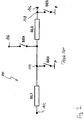
band antenna switch 10 is illustrated. Theantenna switch 10 is part of a mobile telephone operable in three frequency bands in accordance with GSM 900, GSM 1800 andGSM 1900. - The
antenna switch 10 depicted in Fig. 3a has a modular structure and consists essentially of a high-power stage 12, amultiband transformation stage 14 and a low-power stage 16. Asignal output 18 of the high-power stage 12, afirst signal port 20 of themultiband transformation stage 14 and an input/output port configured asantenna port 22 are each coupled to anode 24. Asecond signal port 26 of themultiband transformation stage 14 is connected to asignal input port 28 of the low-power stage 16. - The high-
power stage 12 is constructed in multi-layer technology and is used as a multiband transmitter switch. It comprises afirst signal input 30 and asecond signal input 32 coupled to respective transmitters not depicted in Fig. 3a. Thefirst signal input 30 is used as common GSM 1800 /GSM 1900 signal input, i.e. as high-band signal input. Thesecond input 32 is used as GSM 900 signal input, i.e. as low-band signal input. A first high-power signal path 34 is coupled between the high-band signal input 30 and anode 36. A second high-power signal path 38 is coupled between the low-band signal input 32 and thenode 36. Each high-power signal path pass filter pass filters power stage 12 further comprises an individual biasing network not depicted in Fig. 3 for each pin-diode D3, D4. Each biasing network may be configured like the biasing network depicted in Fig. 1. - The
multiband transformation stage 14 has asingle signal path 50 which connects thefirst signal port 20 and thesecond signal port 26 of themultiband transformation stage 14. Thesignal path 50 is constituted by two signal path portions in the form of a first transmission line T1 and a second transmission line T2 coupled in series. The first transmission line T1 is configured to have approximately a quarter-wavelength charcteristic for the two frequency bands of 1800 MHz and 1900 MHz corresponding to GSM 1800 andGSM 1900. The second transmission line T2 is configured such that the two transmission lines T1 and T2 coupled in series have approximately a quarter-wavelength characteristic for the frequency band of 900 MHz corresponding to GSM 900. - The
multiband transformation stage 14 further comprises two switching elements in the form of pin-diodes D1, D2. The two pin-diodes D1, D2 can be switched independently from each other by means of individual biasing networks not depicted in Fig. 3a. Each biasing network may be configured like the biasing network depicted in Fig. 1 and may comprise an inductor and a resistor. The first pin-diode D1 is coupled between ground and anode 52 connecting the two transmission lines T1, T2. The second pin-diode D2 is coupled between anode 54 and ground. Thenode 54 is further coupled to thesecond signal port 26 of themultiband transformation stage 14 and an end of the second transmission line T2 which faces the low-power stage 16. - The
multiband transformation stage 14 is also constructed in multi-layer technology. In accordance with the modular aspect of the invention, the high-power stage 12 and themultiband transformation stage 14 are realized as individual stages on different substrates. Alternatively, the high-power stage 12 and themultiband transformation stage 14 could be integrated on a single multi-layer substrate. - The low-
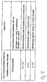
power stage 16 is basically a receive switch matrix with asignal input port 28 coupled to thesecond signal port 26 of themultiband transformation stage 14, threesignal output ports auxiliary port 62. The low-power stage 16 has asignal input 64 for a control signal which specifies which of theports signal input port 28 of the low-power stage 16. The low-power stage 16 has one signal output port for each frequency band. Thesignal output port 56 defines the 1900 MHz signal path and is coupled to a 1900 MHz receiver. Thesignal output port 58 defines the 1800 MHZ signal path and is coupled to a 1800 MHz receiver. Finally, thesignal output port 60 defines the 900 MHz signal path and is coupled to a 900 MHz receiver. The receivers are not depicted in Fig. 3a. Theauxiliary port 62 is terminated with a pre-defined fixed impedance. The function of the auxiliary port will be described later in more detail. - Now, the different operational modes of the
antenna switch 10 are described with reference to the following table:mode state of signal path 50D1 D2 transmit GSM 900 1 OFF ON transmit GSM 1800 / GSM 19002 ON OFF receive GSM 900 / GSM 1800 / GSM 19003 OFF OFF - First, the high-band transmit mode, i.e. transmission in the 1800 MHz band or 1900 MHz band, is described. In the high-band transmit mode either a GSM 1800 transmitter signal or a
GSM 1900 transmitter signal is applied to thefirst signal input 30 of the high-power stage 12. Pin-diode D3 is switched on and pin-diode D4 is switched off. Consequently, either the GSM 1800 transmitter signal or theGSM 1900 transmitter signal is fed to theantenna port 22. In themultiband transformation stage 14 pin-diode D1 is switched on and pin-diode D2 is switched off during high-band transmission. This corresponds to the first state of thesignal path 50 in which the short circuit atnode 52 is transformed by the first transmission line T1, which has a quarter-wavelength transformer characteristic at high-band frequencies, to an open circuit at thefirst signal port 20 of themultiband transformation stage 14. Consequently, the low-power stage 16 remains isolated from thehigh power stage 12 and theantenna port 22. - In the low-band transmit mode a GSM 900 transmitter signal is applied to the
second signal input 32 of the high-power stage 12. Pin-diode D3 is switched off and pin-diode D4 is switched on. Consequently, the GSM 900 transmitter signal is fed to theantenna port 22. In themultiband transformation stage 14 pin-diode D1 is switched off and pin-diode D2 is switched on in the low-band transmission mode. This corresponds to the second state of thesignal path 50 of themultiband transformation stage 14 in which thesignal path 50 has a quarter wavelength transformer characteristic for the 900 MHz transmitter signal. The short circuit atnode 54 is transformed by the two transmission lines T1, T2 to an open circuit at thefirst signal port 20 of themultiband transformation stage 14. Consequently, the low-power stage 16 is isolated from both the high-power stage 12 and theantenna port 22 in the low-band transmit mode. - The low-
power stage 16 is configured as a GaAs MMIC receiver switch matrix. Such GaAs MMIC devices usually generate spurious signals at harmonic frequencies in response to high-power output signals in transmit modes. These spurious signals are generated internally and appear finally at theantenna port 22. However, no further low-pass filtering can be provided at theantenna port 22. Therefore, spurious signals have to be kept below certain limits specified in e.g. the GSM standard. In theantenna switch 10 according to Fig. 3a transmitter signals present atnode 24 are sufficiently attenuated by the amount of isolation provided by themultiband transformation stage 14 such that spurious signal generation within the low-power stage 16 is kept small even without taking further measures. - In the high-band and low-band transmit modes the low-
power stage 16 is switched such that thesignal output 26 of themultiband transformation stage 14 is coupled to theauxiliary port 62 which is terminated with a specific impedance. Such a fixed termination is advantageous because it has been found that stop-band attenuation of the low-pass filters power stage 12 is effected by the impedance present atnode 24. Best transmission performance is achieved when the system impedance of for example 50 Ohm is present atnode 24. In the prior art depicted in Fig. 2, however, it was observed that unused ports like the signal outputs 104, 106 coupled to both thesignal input 102 and corresponding receivers exhibit a varying impedance in the transmit modes. This is due to the fact that receiver filters lead to a mismatch at the signal outputs 104, 106 in the transmit mode. A varying impedance at the signal outputs 104, 106, however, may modify the impedance of the switching elements SE3, SE4, SE5 of themultiband transformation stage 100 such that no effective short circuit is created. Thus no proper transformation to an open circuit impedance at thesignal input 102 of themultiband transformation stage 100 can be achieved. This usually effects the matching of the respective transmitters as well as the performance of low-pass filters within a high-power stage coupled to thesignal input 102. - This problem of prior art antenna switches is overcome by the implementation of the
auxiliary port 62 which allows a fixed termination of thesignal output 26 of themultiband transformation stage 14 in transmit modes. By activating theauxiliary port 62 the impedance atnode 24 can thus be kept constant. Any transmitter signal will therefore be attenuated due to the isolation provided by themultiband transformation stage 14 and additionally by the isolation of the low-power stage 16 with activatedauxiliary port 60. The maximum input power requirements of the receiver filters can be decreased accordingly. High-power receive saw filters are therefore no longer necessary. The size of saw filter structures can thus be reduced. Furthermore, advantages for multi-burst transmit modes as required by general packet radio systems (GPRS) arise. - Up to now the low-band and the high-band transmit mode have been illustrated. Next, the receive mode will be described. The receive mode corresponds to the third state of the
signal path 50 within themultiband transformation stage 14. In the receive mode, all pin-diodes D1, D2, D3, D4 are switched off. Therefore, power consumption of theantenna switch 10 is very low in the receive mode. - Since both pin-diodes D1, D2 of the
multiband transformation stage 14 are switched off in the third state, the two transmission lines T1, T2 can be considered as a pure transmission line without quarter-wavelength transformer characteristic. In the receive mode, one of thesignal output ports antenna port 22 in an impedance-matched manner. - In Fig. 3b a schematic diagram of the second embodiment of a multiband switching device according to the invention in the form of a quadruple-
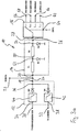
band antenna switch 10 is illustrated. Theantenna switch 10 is part of a mobile telephone operable in four frequency bands in accordance withGSM 450, GSM 900, GSM 1800 andGSM 1900. Theantenna switch 10 depicted in Fig. 3b has some similarities with the antenna switch of Fig. 3a. The same reference numbers are thus used for corresponding components. - Again, the
antenna switch 10 depicted in Fig. 3b has a modular structure and comprises a high-power stage 12, amultiband transformation stage 14 and a low-power stage 16. The high-power stage 16 is constructed in multi-layer technology and is used as a multiband transmitter switch having afirst signal input 30 coupled to aGSM 450 transmitter and asecond signal input 32 coupled to a GSM 900 transmitter. - The
multiband transformation stage 14 is constructed in multi-layer technology. A first transmission line T1 of themultiband transformation stage 14 is configured to have approximately a quarter-wavelength characteristic for the frequency band of 900 MHz corresponding to GSM 900. A second transmission line D2 of themultiband transformation stage 14 is configured such that the two transmission lines T1 and T2 together have approximately a quarter-wavelength characteristic for the frequency band of 450 MHz corresponding toGSM 450. - The low-
power stage 16 is configured as transmit/receive switch matrix with a single signal input/output port 28 coupled to asecond signal port 26 of themultiband transformation stage 14, foursignal output ports signal input port 68, anauxiliary port 62 and acontrol signal input 64. Thesignal output ports auxiliary port 62 is terminated with a pre-defined impedance. - The
input port 68 of the low-power stage 16 is coupled to either a GSM 1800 transmitter path or to aGSM 1900 transmitter path of a transmitter stage not depicted in Fig. 3b. The maximum transmit power occurring at thesignal input 68 is 30 dBm. Thus, the low-power stage 16 may be configured as a GaAs MMIC transmitter/receiver switch matrix. Usually, such GaAs MMIC devices can handle powers up to approximately 30 dBm. Therefore, the value of 30 dBm can serve as a limit with respect to low-power and high-power signals. In future, MMIC devices operable at higher powers will become available. Thus, the limit between low-power signals and high-power signals may shift accordingly. - The operation of the
antenna switch 10 depicted in Fig. 3b is similar to the operation of the antenna switch of Fig. 3a. Therefore, a detailed description is omitted. The different operational modes of theantenna switch 10 depicted in Fig. 3b are shown in the following table:mode state of signal path 50D1 D2 transmit GSM 4501 OFF ON transmit GSM 900 2 ON OFF transmit GSM 1800 / GSM 19003 OFF OFF receive GSM 450 / GSM 900 / GSM 1800 /GSM 19003 OFF OFF - In Fig. 4 a simulation setup for the
antenna switch 10 depicted in Fig. 3a is shown. The simulation is based on measured S-parameter data of pin-diode BAR 63 and additional simulation models available in the HPADS library as shown in Fig. 5. The simulation does not include the low-power stage 16 for selectively coupling thesignal output 26 of themultiband transformation stage 14 to individual receivers or auxiliary ports. Moreover, the low-pass filters power stage 12 have also not been included into the simulation setup. It should be further noted that the simulation setup does not include any components required for biasing the pin-diodes. - As can be seen in Fig. 4, inductors L3 and L4 are connected in parallel to pin-diodes D3 and D4 in order to improve the isolation to the first and
second signal inputs antenna port 22. In the low-band transmit mode a short circuit created by the serious resonance circuit consisting of the parasitic inductance of the pin-diode D2 and of capacitor C2 is also transformed into an open circuit at theantenna port 22. The insertion losses calculated based on the simulation model of Fig. 4 are shown in Fig. 6.
Claims (14)
- A multiband switching device (10), comprising:a multiband transformation stage (14) having:a common first signal port (20) and a common second signal port (26); anda signal path (50) coupled between the first signal port (20) and the second signal port (26), the signal path (50) being switchable via switching elements (D1, D2) between a first state with a first quarter wavelength transformer characteristic for a first transmit mode, a second state with a second quarter-wavelength transformer characteristic for a second transmit mode and a third state with a transmission characteristic for a receive mode,
characterized in that,
the multiband switching device (10) further comprises:a low-power stage (16) comprising:a signal input port (28) coupled to the common second signal port (26) of the multiband transformation stage (14);a first signal output port (56) for being coupled to a receiver operating in a first frequency range;a second signal output port (58) for being coupled to a receiver operating in a second frequency range, the second frequency range differing from the first frequency range;a third signal output port (60) for being coupled to a receiver operating in a third frequency range, the third frequency range differing from the first and second frequency ranges;an auxiliary port (62) that is terminated with a pre-determined impedance; anda signal input (64) to receive a control signal that specifies which of the low-power stage ports (56, 68, 60, 62) is to be coupled to the common second signal port (26) of the multiband transformation stage (14), wherein, depending on the received frequency range, one of the first, second, and third signal ports (56, 58, 60) is coupled when the multiband transformation stage is in the third state, and wherein the auxiliary port (62) is coupled when the multiband transformation stage is in the first and second states. - The multiband switching device (10) of claim 1, wherein only two switching elements (D1, D2) are utilized to switch between each of the first, second, and third states, and that each state requires a maximum of one of the switching elements to be turned on.
- The multiband switching device (10) according to claim 1 or 2, wherein the signal path (50) has a first portion (T1) coupled between the first signal port (20) and a first node (52) and a second portion (T2) coupled between the first node (52) and the second signal port (26), the first portion (T1) having a quarter-wavelength characteristic for the first transmit mode and the first portion (T1) and the second portion (T2) together having a quarter-wavelength characteristic for the second transmit mode.
- The multiband switching device (10) according to claim 3, wherein the second portion (T2) is coupled between the first node (52) and a second node (54) coupled to the second signal port (26) and wherein the multiband transformation stage (14) further comprises, for switching between the three states, a first switching element (D1) coupled to the first node (52) and a second switching element (D2) coupled to the second node (54).
- The multiband switching device (10) according to one of the preceding claims, wherein the multiband transformation stage (14) is constructed in multi-layer technology or with discrete components.
- The multiband switching device (10) according to one of the preceding claims, wherein the low-power stage (16) is a MMIC device.
- The multiband switching device (10) according to one of the preceding claims, wherein the low-power stage (16) is a multiband receiver switch (16) or a multiband transmitter/receiver switch.
- The multiband switching device (10) according to one of the preceding claims, further comprising a high-power stage (12) coupled to the first signal port (20) of the multiband transformation stage (14).
- The multiband switching device (10) according to claim 8, further comprising an input/output port coupled to the high-power stage (12) and the first signal port of the multiband transformation stage (14).
- The multiband switching device (10) according to claim 9, wherein the input/output port is an antenna port (22).
- The multiband switching device (10) according to one of claims 8 to 10, wherein the high-power stage is a multiband transmitter switch (12).
- The multiband switching device according to one of claims 8 to 11, wherein the high-power stage (12) is constructed in multi-layer technology or with discrete components.
- The multiband switching device according to one of the preceding claims, wherein:the first frequency range is approximately centered at 1900 MHz; and / orthe second frequency range is approximately centered at 1800 MHz; and / or the third frequency range is approximately centered at 900 MHz.
- A mobile telephone comprising the multiband switching device (10) according to one of the preceding claims, the multiband switching device (10) being configured as an antenna switch.
Priority Applications (5)
| Application Number | Priority Date | Filing Date | Title |
|---|---|---|---|
| EP01104812A EP1237222B1 (en) | 2001-02-27 | 2001-02-27 | Multiband transformation stage for a multiband r.f. switching device |
| DE60116676T DE60116676T2 (en) | 2001-02-27 | 2001-02-27 | Multi-band transformation stage for a multi-band RF switching device |
| AT01104812T ATE316294T1 (en) | 2001-02-27 | 2001-02-27 | MULTI-BAND TRANSFORMATION STAGE FOR A MULTI-BAND RF SWITCHING DEVICE |
| PCT/EP2002/002090 WO2002069435A1 (en) | 2001-02-27 | 2002-02-27 | Multiband r. f. switching device |
| US10/468,916 US7005940B2 (en) | 2001-02-27 | 2002-02-27 | Multiband R. F. switching device |
Applications Claiming Priority (1)
| Application Number | Priority Date | Filing Date | Title |
|---|---|---|---|
| EP01104812A EP1237222B1 (en) | 2001-02-27 | 2001-02-27 | Multiband transformation stage for a multiband r.f. switching device |
Publications (2)
| Publication Number | Publication Date |
|---|---|
| EP1237222A1 EP1237222A1 (en) | 2002-09-04 |
| EP1237222B1 true EP1237222B1 (en) | 2006-01-18 |
Family
ID=8176620
Family Applications (1)
| Application Number | Title | Priority Date | Filing Date |
|---|---|---|---|
| EP01104812A Expired - Lifetime EP1237222B1 (en) | 2001-02-27 | 2001-02-27 | Multiband transformation stage for a multiband r.f. switching device |
Country Status (5)
| Country | Link |
|---|---|
| US (1) | US7005940B2 (en) |
| EP (1) | EP1237222B1 (en) |
| AT (1) | ATE316294T1 (en) |
| DE (1) | DE60116676T2 (en) |
| WO (1) | WO2002069435A1 (en) |
Families Citing this family (41)
| Publication number | Priority date | Publication date | Assignee | Title |
|---|---|---|---|---|
| WO2004036778A1 (en) * | 2002-10-14 | 2004-04-29 | Koninklijke Philips Electronics N.V. | Transmit and receive antenna switch |
| EP1427115A1 (en) | 2002-12-06 | 2004-06-09 | TDK Corporation | Antenna switching circuit |
| FR2850206B1 (en) | 2003-01-17 | 2005-05-20 | Cit Alcatel | SWITCH DEVICE ONE TRACK TO TWO WITHOUT SINGLE BREAK POINT |
| US20040185795A1 (en) * | 2003-02-05 | 2004-09-23 | Khosro Shamsaifar | Electronically tunable RF Front End Module |
| JPWO2004093346A1 (en) * | 2003-04-17 | 2006-07-06 | 富士通株式会社 | Information processing apparatus and communication apparatus having antenna switching function, antenna switching control apparatus, antenna switching control program, and computer-readable recording medium storing the program |
| US7197284B2 (en) | 2003-04-25 | 2007-03-27 | Telefonaktiebolaget Lm Ericsson (Publ) | Antenna switches including field effect transistors |
| JP4029779B2 (en) * | 2003-06-05 | 2008-01-09 | 株式会社村田製作所 | High frequency module and communication device |
| ATE456194T1 (en) | 2003-07-22 | 2010-02-15 | Nxp Bv | ANTENNA SWITCH WITH ADAPTIVE FILTER |
| JP2005136948A (en) * | 2003-10-08 | 2005-05-26 | Renesas Technology Corp | Antenna switch circuit |
| US6990357B2 (en) * | 2003-10-17 | 2006-01-24 | Nokia Corporation | Front-end arrangements for multiband multimode communication engines |
| US7269441B2 (en) * | 2003-10-17 | 2007-09-11 | Nokia Corporation | Multiband multimode communication engines |
| SE528017C2 (en) | 2004-02-02 | 2006-08-08 | Amc Centurion Ab | Antenna device and portable radio communication device including such antenna device |
| DE102004033268A1 (en) * | 2004-07-09 | 2006-02-02 | Atmel Germany Gmbh | RF circuit |
| US9172404B1 (en) * | 2005-02-07 | 2015-10-27 | Rf Micro Devices, Inc. | Switch architecture for TDMA and FDD multiplexing |
| FR2889006B1 (en) * | 2005-07-22 | 2007-09-21 | St Microelectronics Sa | ANTENNA SWITCH |
| US8213867B2 (en) * | 2005-07-27 | 2012-07-03 | T-Mobile Usa, Inc. | Frequency band adaptive wireless communication |
| US10469205B2 (en) | 2005-07-27 | 2019-11-05 | T-Mobile Usa, Inc. | Application-based multi-band transmission |
| EP1786192A1 (en) * | 2005-11-10 | 2007-05-16 | Alcatel Lucent | Line termination arrangement with combined broadband and narrowband services |
| US7548208B2 (en) * | 2006-02-24 | 2009-06-16 | Palm, Inc. | Internal diversity antenna architecture |
| DE102007021581B4 (en) * | 2007-05-08 | 2018-09-27 | Snaptrack Inc. | Electrical component with a front-end circuit |
| US20080285470A1 (en) * | 2007-05-18 | 2008-11-20 | Catherine Yuan | Determining An Active/Standby State From Service Readiness |
| US7609115B2 (en) * | 2007-09-07 | 2009-10-27 | Raytheon Company | Input circuitry for transistor power amplifier and method for designing such circuitry |
| EP2037530A1 (en) * | 2007-09-13 | 2009-03-18 | Alcatel Lucent | Switchable RF-path and frequency splitter for wide range multiband applications |
| US8897722B2 (en) * | 2009-09-11 | 2014-11-25 | Broadcom Corporation | RF front-end with wideband transmitter/receiver isolation |
| US8514035B2 (en) | 2009-12-30 | 2013-08-20 | Broadcom Corporation | RF front-end with on-chip transmitter/receiver isolation using a gyrator |
| US9331720B2 (en) | 2012-01-30 | 2016-05-03 | Qualcomm Incorporated | Combined directional coupler and impedance matching circuit |
| WO2013125363A1 (en) * | 2012-02-23 | 2013-08-29 | 株式会社村田製作所 | High-frequency module and high-frequency component |
| CN202759442U (en) * | 2012-07-11 | 2013-02-27 | 中兴通讯股份有限公司 | Radio frequency front-end circuit of multifrequency terminal and multifrequency terminal |
| US9024838B2 (en) | 2012-08-09 | 2015-05-05 | Qualcomm Incorporated | Multi-throw antenna switch with off-state capacitance reduction |
| US8774068B2 (en) * | 2012-10-11 | 2014-07-08 | Sony Corporation | Dual swapping switches to meet linearity demands of carrier aggregation |
| US9609575B2 (en) * | 2012-12-31 | 2017-03-28 | T-Mobile Usa, Inc. | Intelligent routing of network packets on telecommunication devices |
| US10375629B2 (en) | 2012-12-31 | 2019-08-06 | T-Mobile Usa, Inc. | Service preferences for multiple-carrier-enabled devices |
| US9729190B2 (en) * | 2014-01-17 | 2017-08-08 | Qualcomm Incorporated | Switchable antenna array |
| US10027366B2 (en) * | 2014-04-25 | 2018-07-17 | Raytheon Company | High power radio frequency (RF) antenna switch |
| US9231550B2 (en) | 2014-06-09 | 2016-01-05 | Mitsubishi Electric Research Laboratories, Inc. | Output matching network for wideband power amplifier with harmonic suppression |
| US10153238B2 (en) * | 2014-08-20 | 2018-12-11 | Samsung Display Co., Ltd. | Electrical channel including pattern voids |
| US11171683B2 (en) | 2018-04-12 | 2021-11-09 | Shenzhen GOODIX Technology Co., Ltd. | Multi-mode configurable transceiver with low voltage switches |
| US10333579B1 (en) * | 2018-04-12 | 2019-06-25 | Shenzhen GOODIX Technology Co., Ltd. | Multi-mode configurable transceiver with low voltage switches |
| US11323147B1 (en) * | 2021-06-07 | 2022-05-03 | Futurecom Systems Group, ULC | Reducing insertion loss in a switch for a communication device |
| US12095496B2 (en) | 2021-10-18 | 2024-09-17 | Futurecom Systems Group, ULC | Self-diagnostic systems and method for a transceiver |
| US12041533B2 (en) | 2022-05-10 | 2024-07-16 | Motorola Solutions, Inc. | System and method for configuring a portable communication system |
Family Cites Families (15)
| Publication number | Priority date | Publication date | Assignee | Title |
|---|---|---|---|---|
| US4701724A (en) | 1986-07-15 | 1987-10-20 | Motorola, Inc. | Injection switch and directional coupler |
| JP2830319B2 (en) * | 1990-03-08 | 1998-12-02 | ソニー株式会社 | Transmission / reception switching device |
| DE69307412T2 (en) * | 1992-07-08 | 1997-06-12 | Matsushita Electric Ind Co Ltd | Antenna switching arrangement for selectively connecting an antenna to a transmitter or a receiver |
| GB2282270B (en) * | 1993-03-31 | 1996-12-04 | Motorola Inc | Switch circuit and method therefor |
| CN1081850C (en) * | 1995-09-29 | 2002-03-27 | 松下电器产业株式会社 | Power amplifier and communication device |
| JP3777209B2 (en) * | 1995-11-14 | 2006-05-24 | 富士通株式会社 | High frequency switch and transmitter / receiver with high frequency switch |
| US6070059A (en) * | 1995-12-05 | 2000-05-30 | Murata Manufacturing Co., Ltd. | High-frequency switch |
| DE19704151C1 (en) * | 1997-02-04 | 1998-08-27 | Siemens Ag | Transmit-receive switching arrangement |
| JPH11340872A (en) * | 1998-05-28 | 1999-12-10 | Kyocera Corp | Dual-band compatible antenna switching circuit |
| DE19842706A1 (en) * | 1998-09-17 | 2000-03-23 | Siemens Ag | Multi-band aerial switch for multi-band mobile radio telephone |
| DE19919368B4 (en) * | 1999-04-28 | 2004-03-18 | Siemens Ag | Mobile radio terminal and method for its operation |
| DK1006669T3 (en) * | 1998-11-30 | 2006-11-27 | Bosch Gmbh Robert | Switchable broadband receiver input stage for a multiband receiver |
| WO2000041326A1 (en) * | 1999-01-07 | 2000-07-13 | Motorola Inc. | A radio frequency (rf) switch using a single quarter wave isolating section and method of forming same |
| EP1153457A1 (en) * | 1999-02-19 | 2001-11-14 | Siemens Aktiengesellschaft | Low attenuating filter/ circuit arrangement |
| JP3772771B2 (en) * | 2001-05-18 | 2006-05-10 | 松下電器産業株式会社 | Multiband high frequency switch |
-
2001
- 2001-02-27 DE DE60116676T patent/DE60116676T2/en not_active Expired - Lifetime
- 2001-02-27 AT AT01104812T patent/ATE316294T1/en not_active IP Right Cessation
- 2001-02-27 EP EP01104812A patent/EP1237222B1/en not_active Expired - Lifetime
-
2002
- 2002-02-27 US US10/468,916 patent/US7005940B2/en not_active Expired - Lifetime
- 2002-02-27 WO PCT/EP2002/002090 patent/WO2002069435A1/en not_active Ceased
Also Published As
| Publication number | Publication date |
|---|---|
| EP1237222A1 (en) | 2002-09-04 |
| US20040092285A1 (en) | 2004-05-13 |
| WO2002069435A1 (en) | 2002-09-06 |
| US7005940B2 (en) | 2006-02-28 |
| DE60116676D1 (en) | 2006-04-06 |
| ATE316294T1 (en) | 2006-02-15 |
| DE60116676T2 (en) | 2006-10-19 |
Similar Documents
| Publication | Publication Date | Title |
|---|---|---|
| EP1237222B1 (en) | Multiband transformation stage for a multiband r.f. switching device | |
| US6496083B1 (en) | Diode compensation circuit including two series and one parallel resonance points | |
| KR100671651B1 (en) | Harmonic suppression apparatus and method for dual band mobile phone | |
| US7035602B2 (en) | High-frequency composite switch component | |
| US7142884B2 (en) | Combined front-end circuit for wireless transmission systems | |
| US8264297B2 (en) | Balun signal splitter | |
| US6928298B2 (en) | Mobile communication device and high-frequency composite unit used in the same | |
| US6317608B1 (en) | Power amplifier matching in dual band mobile phone | |
| US7756488B2 (en) | High-frequency switch module | |
| US7239853B2 (en) | Antenna switching circuit | |
| EP1237290B1 (en) | Antenna duplexer and mobile communication device using the same | |
| US9998153B2 (en) | Front-end module for carrier aggregation mode | |
| EP1532745B1 (en) | High frequency module | |
| JP3810011B2 (en) | High frequency switch module and multilayer substrate for high frequency switch module | |
| US7454178B2 (en) | Low-loss transmitter module | |
| EP0964477B1 (en) | Antenna sharing device for dual frequency band | |
| JP2008522533A (en) | Distributed diplexer | |
| JP4216080B2 (en) | Antenna interface unit | |
| JP3866989B2 (en) | Antenna duplexer and mobile communication device using the same | |
| GB2375905A (en) | A GSM-DCS dual-band transmit-receive switch for a mobile telephone | |
| HK1024108B (en) | Antenna sharing device for dual frequency band |
Legal Events
| Date | Code | Title | Description |
|---|---|---|---|
| PUAI | Public reference made under article 153(3) epc to a published international application that has entered the european phase |
Free format text: ORIGINAL CODE: 0009012 |
|
| AK | Designated contracting states |
Kind code of ref document: A1 Designated state(s): AT BE CH CY DE DK ES FI FR GB GR IE IT LI LU MC NL PT SE TR |
|
| AX | Request for extension of the european patent |
Free format text: AL;LT;LV;MK;RO;SI |
|
| 17P | Request for examination filed |
Effective date: 20030128 |
|
| AKX | Designation fees paid |
Designated state(s): AT BE CH CY DE DK ES FI FR GB GR IE IT LI LU MC NL PT SE TR |
|
| 17Q | First examination report despatched |
Effective date: 20031209 |
|
| RAP1 | Party data changed (applicant data changed or rights of an application transferred) |
Owner name: TELEFONAKTIEBOLAGET LM ERICSSON (PUBL) |
|
| GRAP | Despatch of communication of intention to grant a patent |
Free format text: ORIGINAL CODE: EPIDOSNIGR1 |
|
| GRAS | Grant fee paid |
Free format text: ORIGINAL CODE: EPIDOSNIGR3 |
|
| GRAA | (expected) grant |
Free format text: ORIGINAL CODE: 0009210 |
|
| AK | Designated contracting states |
Kind code of ref document: B1 Designated state(s): AT BE CH CY DE DK ES FI FR GB GR IE IT LI LU MC NL PT SE TR |
|
| PG25 | Lapsed in a contracting state [announced via postgrant information from national office to epo] |
Ref country code: LI Free format text: LAPSE BECAUSE OF FAILURE TO SUBMIT A TRANSLATION OF THE DESCRIPTION OR TO PAY THE FEE WITHIN THE PRESCRIBED TIME-LIMIT Effective date: 20060118 Ref country code: IT Free format text: LAPSE BECAUSE OF FAILURE TO SUBMIT A TRANSLATION OF THE DESCRIPTION OR TO PAY THE FEE WITHIN THE PRESCRIBED TIME-LIMIT;WARNING: LAPSES OF ITALIAN PATENTS WITH EFFECTIVE DATE BEFORE 2007 MAY HAVE OCCURRED AT ANY TIME BEFORE 2007. THE CORRECT EFFECTIVE DATE MAY BE DIFFERENT FROM THE ONE RECORDED. Effective date: 20060118 Ref country code: NL Free format text: LAPSE BECAUSE OF FAILURE TO SUBMIT A TRANSLATION OF THE DESCRIPTION OR TO PAY THE FEE WITHIN THE PRESCRIBED TIME-LIMIT Effective date: 20060118 Ref country code: BE Free format text: LAPSE BECAUSE OF FAILURE TO SUBMIT A TRANSLATION OF THE DESCRIPTION OR TO PAY THE FEE WITHIN THE PRESCRIBED TIME-LIMIT Effective date: 20060118 Ref country code: CH Free format text: LAPSE BECAUSE OF FAILURE TO SUBMIT A TRANSLATION OF THE DESCRIPTION OR TO PAY THE FEE WITHIN THE PRESCRIBED TIME-LIMIT Effective date: 20060118 Ref country code: FI Free format text: LAPSE BECAUSE OF FAILURE TO SUBMIT A TRANSLATION OF THE DESCRIPTION OR TO PAY THE FEE WITHIN THE PRESCRIBED TIME-LIMIT Effective date: 20060118 Ref country code: AT Free format text: LAPSE BECAUSE OF FAILURE TO SUBMIT A TRANSLATION OF THE DESCRIPTION OR TO PAY THE FEE WITHIN THE PRESCRIBED TIME-LIMIT Effective date: 20060118 |
|
| REG | Reference to a national code |
Ref country code: GB Ref legal event code: FG4D |
|
| REG | Reference to a national code |
Ref country code: CH Ref legal event code: EP |
|
| REG | Reference to a national code |
Ref country code: IE Ref legal event code: FG4D |
|
| PG25 | Lapsed in a contracting state [announced via postgrant information from national office to epo] |
Ref country code: IE Free format text: LAPSE BECAUSE OF NON-PAYMENT OF DUE FEES Effective date: 20060227 |
|
| PG25 | Lapsed in a contracting state [announced via postgrant information from national office to epo] |
Ref country code: MC Free format text: LAPSE BECAUSE OF NON-PAYMENT OF DUE FEES Effective date: 20060228 |
|
| PG25 | Lapsed in a contracting state [announced via postgrant information from national office to epo] |
Ref country code: LU Free format text: LAPSE BECAUSE OF NON-PAYMENT OF DUE FEES Effective date: 20060318 |
|
| REF | Corresponds to: |
Ref document number: 60116676 Country of ref document: DE Date of ref document: 20060406 Kind code of ref document: P |
|
| PG25 | Lapsed in a contracting state [announced via postgrant information from national office to epo] |
Ref country code: SE Free format text: LAPSE BECAUSE OF FAILURE TO SUBMIT A TRANSLATION OF THE DESCRIPTION OR TO PAY THE FEE WITHIN THE PRESCRIBED TIME-LIMIT Effective date: 20060418 Ref country code: GB Free format text: LAPSE BECAUSE OF NON-PAYMENT OF DUE FEES Effective date: 20060418 Ref country code: DK Free format text: LAPSE BECAUSE OF FAILURE TO SUBMIT A TRANSLATION OF THE DESCRIPTION OR TO PAY THE FEE WITHIN THE PRESCRIBED TIME-LIMIT Effective date: 20060418 |
|
| PG25 | Lapsed in a contracting state [announced via postgrant information from national office to epo] |
Ref country code: ES Free format text: LAPSE BECAUSE OF FAILURE TO SUBMIT A TRANSLATION OF THE DESCRIPTION OR TO PAY THE FEE WITHIN THE PRESCRIBED TIME-LIMIT Effective date: 20060429 |
|
| PG25 | Lapsed in a contracting state [announced via postgrant information from national office to epo] |
Ref country code: PT Free format text: LAPSE BECAUSE OF FAILURE TO SUBMIT A TRANSLATION OF THE DESCRIPTION OR TO PAY THE FEE WITHIN THE PRESCRIBED TIME-LIMIT Effective date: 20060619 |
|
| NLV1 | Nl: lapsed or annulled due to failure to fulfill the requirements of art. 29p and 29m of the patents act | ||
| REG | Reference to a national code |
Ref country code: CH Ref legal event code: PL |
|
| PLBE | No opposition filed within time limit |
Free format text: ORIGINAL CODE: 0009261 |
|
| STAA | Information on the status of an ep patent application or granted ep patent |
Free format text: STATUS: NO OPPOSITION FILED WITHIN TIME LIMIT |
|
| 26N | No opposition filed |
Effective date: 20061019 |
|
| GBPC | Gb: european patent ceased through non-payment of renewal fee |
Effective date: 20060418 |
|
| EN | Fr: translation not filed | ||
| PG25 | Lapsed in a contracting state [announced via postgrant information from national office to epo] |
Ref country code: FR Free format text: LAPSE BECAUSE OF FAILURE TO SUBMIT A TRANSLATION OF THE DESCRIPTION OR TO PAY THE FEE WITHIN THE PRESCRIBED TIME-LIMIT Effective date: 20070309 Ref country code: GR Free format text: LAPSE BECAUSE OF FAILURE TO SUBMIT A TRANSLATION OF THE DESCRIPTION OR TO PAY THE FEE WITHIN THE PRESCRIBED TIME-LIMIT Effective date: 20060419 |
|
| PG25 | Lapsed in a contracting state [announced via postgrant information from national office to epo] |
Ref country code: TR Free format text: LAPSE BECAUSE OF FAILURE TO SUBMIT A TRANSLATION OF THE DESCRIPTION OR TO PAY THE FEE WITHIN THE PRESCRIBED TIME-LIMIT Effective date: 20060118 |
|
| PG25 | Lapsed in a contracting state [announced via postgrant information from national office to epo] |
Ref country code: FR Free format text: LAPSE BECAUSE OF FAILURE TO SUBMIT A TRANSLATION OF THE DESCRIPTION OR TO PAY THE FEE WITHIN THE PRESCRIBED TIME-LIMIT Effective date: 20060228 |
|
| PG25 | Lapsed in a contracting state [announced via postgrant information from national office to epo] |
Ref country code: CY Free format text: LAPSE BECAUSE OF FAILURE TO SUBMIT A TRANSLATION OF THE DESCRIPTION OR TO PAY THE FEE WITHIN THE PRESCRIBED TIME-LIMIT Effective date: 20060118 Ref country code: FR Free format text: LAPSE BECAUSE OF FAILURE TO SUBMIT A TRANSLATION OF THE DESCRIPTION OR TO PAY THE FEE WITHIN THE PRESCRIBED TIME-LIMIT Effective date: 20060118 |
|
| PGFP | Annual fee paid to national office [announced via postgrant information from national office to epo] |
Ref country code: DE Payment date: 20200227 Year of fee payment: 20 |
|
| REG | Reference to a national code |
Ref country code: DE Ref legal event code: R071 Ref document number: 60116676 Country of ref document: DE |