EP1237222B1 - Mehrband-Transformationsstufe für eine Mehrband-HF-Umschaltvorrichtung - Google Patents
Mehrband-Transformationsstufe für eine Mehrband-HF-Umschaltvorrichtung Download PDFInfo
- Publication number
- EP1237222B1 EP1237222B1 EP01104812A EP01104812A EP1237222B1 EP 1237222 B1 EP1237222 B1 EP 1237222B1 EP 01104812 A EP01104812 A EP 01104812A EP 01104812 A EP01104812 A EP 01104812A EP 1237222 B1 EP1237222 B1 EP 1237222B1
- Authority
- EP
- European Patent Office
- Prior art keywords
- multiband
- signal
- port
- coupled
- switching device
- Prior art date
- Legal status (The legal status is an assumption and is not a legal conclusion. Google has not performed a legal analysis and makes no representation as to the accuracy of the status listed.)
- Expired - Lifetime
Links
- 230000009466 transformation Effects 0.000 title claims abstract description 97
- 230000005540 biological transmission Effects 0.000 claims abstract description 34
- 238000005516 engineering process Methods 0.000 claims description 9
- 238000004088 simulation Methods 0.000 description 12
- 238000002955 isolation Methods 0.000 description 9
- 238000010586 diagram Methods 0.000 description 7
- 230000008878 coupling Effects 0.000 description 6
- 238000010168 coupling process Methods 0.000 description 6
- 238000005859 coupling reaction Methods 0.000 description 6
- 229910001218 Gallium arsenide Inorganic materials 0.000 description 4
- 239000011159 matrix material Substances 0.000 description 4
- 230000002238 attenuated effect Effects 0.000 description 2
- 239000003990 capacitor Substances 0.000 description 2
- 230000009977 dual effect Effects 0.000 description 2
- 230000003071 parasitic effect Effects 0.000 description 2
- 239000000758 substrate Substances 0.000 description 2
- 230000003213 activating effect Effects 0.000 description 1
- 238000010276 construction Methods 0.000 description 1
- 230000003247 decreasing effect Effects 0.000 description 1
- 230000001419 dependent effect Effects 0.000 description 1
- 230000000694 effects Effects 0.000 description 1
- 230000002708 enhancing effect Effects 0.000 description 1
- 238000001914 filtration Methods 0.000 description 1
- 230000007274 generation of a signal involved in cell-cell signaling Effects 0.000 description 1
- 238000003780 insertion Methods 0.000 description 1
- 230000037431 insertion Effects 0.000 description 1
- 238000010295 mobile communication Methods 0.000 description 1
- 230000000644 propagated effect Effects 0.000 description 1
- 238000012358 sourcing Methods 0.000 description 1
Images


Classifications
-
- H—ELECTRICITY
- H04—ELECTRIC COMMUNICATION TECHNIQUE
- H04B—TRANSMISSION
- H04B1/00—Details of transmission systems, not covered by a single one of groups H04B3/00 - H04B13/00; Details of transmission systems not characterised by the medium used for transmission
- H04B1/005—Details of transmission systems, not covered by a single one of groups H04B3/00 - H04B13/00; Details of transmission systems not characterised by the medium used for transmission adapting radio receivers, transmitters andtransceivers for operation on two or more bands, i.e. frequency ranges
- H04B1/0053—Details of transmission systems, not covered by a single one of groups H04B3/00 - H04B13/00; Details of transmission systems not characterised by the medium used for transmission adapting radio receivers, transmitters andtransceivers for operation on two or more bands, i.e. frequency ranges with common antenna for more than one band
- H04B1/006—Details of transmission systems, not covered by a single one of groups H04B3/00 - H04B13/00; Details of transmission systems not characterised by the medium used for transmission adapting radio receivers, transmitters andtransceivers for operation on two or more bands, i.e. frequency ranges with common antenna for more than one band using switches for selecting the desired band
-
- H—ELECTRICITY
- H01—ELECTRIC ELEMENTS
- H01P—WAVEGUIDES; RESONATORS, LINES, OR OTHER DEVICES OF THE WAVEGUIDE TYPE
- H01P1/00—Auxiliary devices
- H01P1/10—Auxiliary devices for switching or interrupting
- H01P1/15—Auxiliary devices for switching or interrupting by semiconductor devices
-
- H—ELECTRICITY
- H01—ELECTRIC ELEMENTS
- H01P—WAVEGUIDES; RESONATORS, LINES, OR OTHER DEVICES OF THE WAVEGUIDE TYPE
- H01P5/00—Coupling devices of the waveguide type
- H01P5/04—Coupling devices of the waveguide type with variable factor of coupling
-
- H—ELECTRICITY
- H04—ELECTRIC COMMUNICATION TECHNIQUE
- H04B—TRANSMISSION
- H04B1/00—Details of transmission systems, not covered by a single one of groups H04B3/00 - H04B13/00; Details of transmission systems not characterised by the medium used for transmission
- H04B1/005—Details of transmission systems, not covered by a single one of groups H04B3/00 - H04B13/00; Details of transmission systems not characterised by the medium used for transmission adapting radio receivers, transmitters andtransceivers for operation on two or more bands, i.e. frequency ranges
-
- H—ELECTRICITY
- H04—ELECTRIC COMMUNICATION TECHNIQUE
- H04B—TRANSMISSION
- H04B1/00—Details of transmission systems, not covered by a single one of groups H04B3/00 - H04B13/00; Details of transmission systems not characterised by the medium used for transmission
- H04B1/38—Transceivers, i.e. devices in which transmitter and receiver form a structural unit and in which at least one part is used for functions of transmitting and receiving
- H04B1/40—Circuits
- H04B1/44—Transmit/receive switching
Definitions
- the antenna switch for coupling a single antenna to either one of a first and a second receiver, operable at a first and a second frequency band, respectively, and a first and a second transmitter, operable to transmit at the first and the second frequency band, respectively, is known from DE 197 04 151.
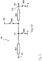
- the antenna switch has a multiband transformation stage 100 as schematically depicted in Fig. 2.
- the multiband transformation stage 100 comprises a common signal input 102, two separate signal outputs 104, 106, two quarter-wavelength transformers SL1, SL2 coupled in series and three switching elements SE3, SE4, SE5.
- the two quarter-wavelength transformers SL1, SL2 coupled in series represent together a quarter-wavelength transmission line at a first frequency band and each single quarter-wavelength transformer SL1, SL2 represents a quarter-wavelength transmission line for a second frequency band equaling approximately twice the first frequency band.
- the multiband transformation stage 100 has four operational states. In a first operational state corresponding to transmission in the first frequency band, switching elements SE3 and SE4 are switched off and switching element SE5 is switched on. The short circuit created by switching element SE5 at a node 108 is transformed to an open circuit for the first frequency band at signal input 102 of the multiband transformation stage 100. In a second operational mode corresponding to transmission in the second frequency band, switching element SE3 is switched on and switching elements SE4 and SE5 are switched off. Switching element SE3 thus creates a short circuit at a node 110. This short circuit is transformed by the quarter-wavelength transmission line SL1 to an open circuit for the second frequency band at signal input 102.
- the low-power stage can be a low-power switch comprising a first signal port coupled to the second signal port of the multiband transformation stage and further comprising a plurality of second signal ports which may be coupled to the first signal port of the low-power switch.
- the single signal path of the multiband transformation stage can selectively be connected to one of the plurality of second signal ports of the low-power switch.
- the low-power switch may have an individual signal input or output port for each frequency band.
- the low-power switch may thus comprise three corresponding second signal ports configured as signal output ports.
- the low-power switch may have additional second signal input or output ports for signals such as a low-power transmitter signal, a global positioning system (GPS) signal or a Bluetooth signal.
- GPS global positioning system
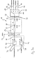
- Fig. 3a a schematic diagram of a first embodiment of a multiband switching device according to the invention in the form of a triple-band antenna switch 10 is illustrated.
- the antenna switch 10 is part of a mobile telephone operable in three frequency bands in accordance with GSM 900, GSM 1800 and GSM 1900.
- the signal output port 60 defines the 900 MHz signal path and is coupled to a 900 MHz receiver.
- the receivers are not depicted in Fig. 3a.
- the auxiliary port 62 is terminated with a pre-defined fixed impedance. The function of the auxiliary port will be described later in more detail.
- the antenna switch 10 depicted in Fig. 3b has a modular structure and comprises a high-power stage 12, a multiband transformation stage 14 and a low-power stage 16.
- the high-power stage 16 is constructed in multi-layer technology and is used as a multiband transmitter switch having a first signal input 30 coupled to a GSM 450 transmitter and a second signal input 32 coupled to a GSM 900 transmitter.
- the low-power stage 16 is configured as transmit/receive switch matrix with a single signal input/output port 28 coupled to a second signal port 26 of the multiband transformation stage 14, four signal output ports 56, 58, 60, 66, a signal input port 68, an auxiliary port 62 and a control signal input 64.
- the signal output ports 56, 58, 60, 66 are coupled to a 1900 MHz receiver, a 1800 MHz receiver a 900 MHz receiver and a 450 MHz receiver, respectively.
- the receivers are not depicted in Fig. 3a.
- the auxiliary port 62 is terminated with a pre-defined impedance.
Landscapes
- Engineering & Computer Science (AREA)
- Computer Networks & Wireless Communication (AREA)
- Signal Processing (AREA)
- Transceivers (AREA)
- Transmitters (AREA)
- Amplifiers (AREA)
- Input Circuits Of Receivers And Coupling Of Receivers And Audio Equipment (AREA)
Claims (14)
- Mehrband-Umschaltvorrichtung (10), umfassend:eine Mehrband-Wandlerstufe (14) mit:einem gemeinsamen ersten Signalanschluss (20) und einem gemeinsamen zweiten Signalanschluss (26); undeinem Signalpfad (50), der zwischen dem ersten Signalanschluss (20) und dem zweiten Signalanschluss (26) eingekoppelt ist, wobei der Signalpfad (50) über Schaltelemente (D1, D2) umschaltbar ist zwischen einem ersten Zustand mit einer ersten λ/4-Wandlereigenschaft für einen ersten Sendemodus, einem zweiten Zustand mit einer zweiten λ/4-Wandlereigenschaft für einen zweiten Sendemodus und einem dritten Zustand mit einer Übertragungseigenschaft für einen Empfangsmodus,
dadurch gekennzeichnet, dass
die Mehrband-Umschaltvorrichtung (10) weiterhin umfasst:eine Niedrigleistungsstufe (16), umfassend:einen Signaleingangsanschluss (28), der mit dem gemeinsamen zweiten Signalanschluss (26) der Mehrband-Wandlerstufe (14) gekoppelt ist;einen ersten Signalausgangsanschluss (56), der zum Koppeln mit einem Empfänger vorgesehen ist, welcher in einem ersten Frequenzbereich arbeitet; einen zweiten Signalausgangsanschluss (58), der zum Koppeln mit einem Empfänger vorgesehen ist, welcher in einem zweiten Frequenzbereich arbeitet, wobei das zweite Frequenzband sich vom ersten Frequenzband unterscheidet; einen dritten Signalausgangsanschluss (60), der zum Koppeln mit einem Empfänger vorgesehen ist, welcher in einem dritten Frequenzbereich arbeitet, wobei das dritte Frequenzband sich vom ersten und zweiten Frequenzband unterscheidet;einen Hilfsanschluss (62), der mit einer vorbestimmten Impedanz abschliesst; undeinen Signaleingang (64) zum Empfangen eines Steuersignals, das festlegt, welcher der Niedrigleistungsstufenanschlüsse (56, 58, 60, 62) mit dem gemeinsamen zweiten Signalanschluss (26) der Mehrband-Wandlerstufe (14) zu koppeln ist, wobei abhängig von dem empfangenen Frequenzbereich einer von dem ersten, dem zweiten und dem dritten Signalanschluss (56, 58, 60) angekoppelt wird, wenn die Mehrband-Wandlerstufe sich im dritten Zustand befindet, und wobei der Hilfsanschluss (62) angekoppelt wird, wenn sich die Mehrband-Wandlerstufe in dem ersten und dem zweiten Zustand befindet. - Mehrband-Umschaltvorrichtung (10) nach Anspruch 1, wobei nur zwei Schaltelemente (D1, D2) verwendet werden, um zwischen jedem der ersten, zweiten und dritten Zustände umzuschalten, und wobei jeder Zustand maximal eines der Schaltelemente benötigt, um angeschaltet zu werden.
- Mehrband-Umschaltvorrichtung (10) nach Anspruch 1 oder 2, wobei der Signalpfad (50) einen ersten Abschnitt (T1) ausweist, der zwischen dem ersten Signalanschluss (20) und einem ersten Knoten (52) eingekoppelt ist, sowie einen zweiten Abschnitt (T2), der zwischen dem ersten Knoten (52) und dem zweiten Signalanschluss (26) eingekoppelt ist, wobei der erste Abschnitt (T1) eine λ/4-Eigenschaft für den ersten Sendemodus aufweist und der erste Abschnitt (T1) und der zweite Abschnitt (T2) zusammen eine λ/4-Eigenschaft für den zweiten Sendemodus aufweisen.
- Mehrband-Umschaltvorrichtung (10) nach Anspruch 3, wobei der zweite Abschnitt (T2) zwischen dem ersten Knoten (52) und einem zweiten Knoten (54), der mit dem zweiten Signalanschluss (26) gekoppelt ist, eingekoppelt ist, und wobei die Mehrband-Wandlerstufe (14) zum Umschalten zwischen den drei Zuständen weiterhin ein mit dem ersten Knoten (52) gekoppeltes erstes Schaltelement (D1) und ein mit dem zweiten Knoten (54) gekoppeltes zweites Schaltelement (D2) umfasst.
- Mehrband-Umschaltvorrichtung (10) nach einem der vorhergehenden Ansprüche, wobei die Mehrband-Wandlerstufe (14) in Mehrschichttechnik oder mit diskreten Elementen aufgebaut ist.
- Mehrband-Umschaltvorrichtung (10) nach einem der vorhergehenden Ansprüche, wobei die Niedrigleistungsstufe (16) eine MMIC-Vorrichtung ist.
- Mehrband-Umschaltvorrichtung (10) nach einem der vorhergehenden Ansprüche, wobei die Niedrigleistungsstufe (16) ein Mehrband-Empfangsschalter (16) oder ein Mehrband-Sende/Empfangs-Schalter ist.
- Mehrband-Umschaltvorrichtung (10) nach einem der vorhergehenden Ansprüche, weiterhin umfassend eine Hochleistungsstufe (12), die mit dem ersten Signalanschluss (20) der Mehrband-Wandlerstufe (14) gekoppelt ist.
- Mehrband-Umschaltvorrichtung (10) nach Anspruch 8, weiterhin umfassend einen Eingangs/Ausgangs-Anschluss, der mit der Hochleistungsstufe (12) und dem ersten Signalanschluss der Mehrband-Wandlerstufe (14) gekoppelt ist.
- Mehrband-Umschaltvorrichtung (10) nach Anspruch 9, wobei der Eingangs/Ausgangs-Anschluss ein Antennenanschluss (22) ist.
- Mehrband-Umschaltvorrichtung (10) nach einem der Ansprüche 8 bis 10, wobei die Hochleistungsstufe ein Mehrband-Sendeschalter (12) ist.
- Mehrband-Umschaltvorrichtung nach einem Ansprüche 8 bis 11, wobei die Hochleistungsstufe (12) in Mehrschichttechnik oder mit diskreten Elementen aufgebaut ist.
- Mehrband-Umschaltvorrichtung nach einem der vorhergehenden Ansprüche, wobei:der erste Frequenzbereich ungefähr um 1900 MHz herum zentriert ist; und / oderder zweite Frequenzbereich ungefähr um 1800 MHz herum zentriert ist; und / oderder dritte Frequenzbereich ungefähr um 900 MHz herum zentriert ist.
- Mobiltelefon, umfassend die Mehrband-Umschaltvorrichtung (10) nach einem der vorhergehenden Ansprüche, wobei die Mehrband-Umschaltvorrichtung (10) als ein Antennenschalter konfiguriert ist.
Priority Applications (5)
| Application Number | Priority Date | Filing Date | Title |
|---|---|---|---|
| EP01104812A EP1237222B1 (de) | 2001-02-27 | 2001-02-27 | Mehrband-Transformationsstufe für eine Mehrband-HF-Umschaltvorrichtung |
| DE60116676T DE60116676T2 (de) | 2001-02-27 | 2001-02-27 | Mehrband-Transformationsstufe für eine Mehrband-HF-Umschaltvorrichtung |
| AT01104812T ATE316294T1 (de) | 2001-02-27 | 2001-02-27 | Mehrband-transformationsstufe für eine mehrband- hf-umschaltvorrichtung |
| PCT/EP2002/002090 WO2002069435A1 (en) | 2001-02-27 | 2002-02-27 | Multiband r. f. switching device |
| US10/468,916 US7005940B2 (en) | 2001-02-27 | 2002-02-27 | Multiband R. F. switching device |
Applications Claiming Priority (1)
| Application Number | Priority Date | Filing Date | Title |
|---|---|---|---|
| EP01104812A EP1237222B1 (de) | 2001-02-27 | 2001-02-27 | Mehrband-Transformationsstufe für eine Mehrband-HF-Umschaltvorrichtung |
Publications (2)
| Publication Number | Publication Date |
|---|---|
| EP1237222A1 EP1237222A1 (de) | 2002-09-04 |
| EP1237222B1 true EP1237222B1 (de) | 2006-01-18 |
Family
ID=8176620
Family Applications (1)
| Application Number | Title | Priority Date | Filing Date |
|---|---|---|---|
| EP01104812A Expired - Lifetime EP1237222B1 (de) | 2001-02-27 | 2001-02-27 | Mehrband-Transformationsstufe für eine Mehrband-HF-Umschaltvorrichtung |
Country Status (5)
| Country | Link |
|---|---|
| US (1) | US7005940B2 (de) |
| EP (1) | EP1237222B1 (de) |
| AT (1) | ATE316294T1 (de) |
| DE (1) | DE60116676T2 (de) |
| WO (1) | WO2002069435A1 (de) |
Families Citing this family (41)
| Publication number | Priority date | Publication date | Assignee | Title |
|---|---|---|---|---|
| WO2004036778A1 (en) * | 2002-10-14 | 2004-04-29 | Koninklijke Philips Electronics N.V. | Transmit and receive antenna switch |
| EP1427115A1 (de) | 2002-12-06 | 2004-06-09 | TDK Corporation | Antennenumschaltvorrichtung |
| FR2850206B1 (fr) | 2003-01-17 | 2005-05-20 | Cit Alcatel | Dispositif de commutation une voie vers deux sans point de panne unique |
| US20040185795A1 (en) * | 2003-02-05 | 2004-09-23 | Khosro Shamsaifar | Electronically tunable RF Front End Module |
| JPWO2004093346A1 (ja) * | 2003-04-17 | 2006-07-06 | 富士通株式会社 | アンテナ切替機能を有する情報処理装置および通信装置並びにアンテナ切替制御装置,アンテナ切替制御プログラムおよび同プログラムを記録したコンピュータ読取可能な記録媒体 |
| US7197284B2 (en) | 2003-04-25 | 2007-03-27 | Telefonaktiebolaget Lm Ericsson (Publ) | Antenna switches including field effect transistors |
| JP4029779B2 (ja) * | 2003-06-05 | 2008-01-09 | 株式会社村田製作所 | 高周波モジュールおよび通信装置 |
| ATE456194T1 (de) | 2003-07-22 | 2010-02-15 | Nxp Bv | Antennenschalter mit adaptivem filter |
| JP2005136948A (ja) * | 2003-10-08 | 2005-05-26 | Renesas Technology Corp | アンテナスイッチ回路 |
| US6990357B2 (en) * | 2003-10-17 | 2006-01-24 | Nokia Corporation | Front-end arrangements for multiband multimode communication engines |
| US7269441B2 (en) * | 2003-10-17 | 2007-09-11 | Nokia Corporation | Multiband multimode communication engines |
| SE528017C2 (sv) | 2004-02-02 | 2006-08-08 | Amc Centurion Ab | Antennanordning och bärbar radiokommunikationsanordning innefattande sådan antennanordning |
| DE102004033268A1 (de) * | 2004-07-09 | 2006-02-02 | Atmel Germany Gmbh | Hochfrequenzschaltung |
| US9172404B1 (en) * | 2005-02-07 | 2015-10-27 | Rf Micro Devices, Inc. | Switch architecture for TDMA and FDD multiplexing |
| FR2889006B1 (fr) * | 2005-07-22 | 2007-09-21 | St Microelectronics Sa | Commutateur d'antenne |
| US8213867B2 (en) * | 2005-07-27 | 2012-07-03 | T-Mobile Usa, Inc. | Frequency band adaptive wireless communication |
| US10469205B2 (en) | 2005-07-27 | 2019-11-05 | T-Mobile Usa, Inc. | Application-based multi-band transmission |
| EP1786192A1 (de) * | 2005-11-10 | 2007-05-16 | Alcatel Lucent | Leitungsabschlussanordnung mit kombinierten schmal- und breitbandigen Diensten |
| US7548208B2 (en) * | 2006-02-24 | 2009-06-16 | Palm, Inc. | Internal diversity antenna architecture |
| DE102007021581B4 (de) * | 2007-05-08 | 2018-09-27 | Snaptrack Inc. | Elektrisches Bauelement mit einer Frontend-Schaltung |
| US20080285470A1 (en) * | 2007-05-18 | 2008-11-20 | Catherine Yuan | Determining An Active/Standby State From Service Readiness |
| US7609115B2 (en) * | 2007-09-07 | 2009-10-27 | Raytheon Company | Input circuitry for transistor power amplifier and method for designing such circuitry |
| EP2037530A1 (de) * | 2007-09-13 | 2009-03-18 | Alcatel Lucent | Umschaltbarer HF-Weg und Frequenzteiler für verschiedenste Multibandanwendungen |
| US8897722B2 (en) * | 2009-09-11 | 2014-11-25 | Broadcom Corporation | RF front-end with wideband transmitter/receiver isolation |
| US8514035B2 (en) | 2009-12-30 | 2013-08-20 | Broadcom Corporation | RF front-end with on-chip transmitter/receiver isolation using a gyrator |
| US9331720B2 (en) | 2012-01-30 | 2016-05-03 | Qualcomm Incorporated | Combined directional coupler and impedance matching circuit |
| WO2013125363A1 (ja) * | 2012-02-23 | 2013-08-29 | 株式会社村田製作所 | 高周波モジュールおよび高周波部品 |
| CN202759442U (zh) * | 2012-07-11 | 2013-02-27 | 中兴通讯股份有限公司 | 一种多频终端射频前端电路及多频终端 |
| US9024838B2 (en) | 2012-08-09 | 2015-05-05 | Qualcomm Incorporated | Multi-throw antenna switch with off-state capacitance reduction |
| US8774068B2 (en) * | 2012-10-11 | 2014-07-08 | Sony Corporation | Dual swapping switches to meet linearity demands of carrier aggregation |
| US9609575B2 (en) * | 2012-12-31 | 2017-03-28 | T-Mobile Usa, Inc. | Intelligent routing of network packets on telecommunication devices |
| US10375629B2 (en) | 2012-12-31 | 2019-08-06 | T-Mobile Usa, Inc. | Service preferences for multiple-carrier-enabled devices |
| US9729190B2 (en) * | 2014-01-17 | 2017-08-08 | Qualcomm Incorporated | Switchable antenna array |
| US10027366B2 (en) * | 2014-04-25 | 2018-07-17 | Raytheon Company | High power radio frequency (RF) antenna switch |
| US9231550B2 (en) | 2014-06-09 | 2016-01-05 | Mitsubishi Electric Research Laboratories, Inc. | Output matching network for wideband power amplifier with harmonic suppression |
| US10153238B2 (en) * | 2014-08-20 | 2018-12-11 | Samsung Display Co., Ltd. | Electrical channel including pattern voids |
| US11171683B2 (en) | 2018-04-12 | 2021-11-09 | Shenzhen GOODIX Technology Co., Ltd. | Multi-mode configurable transceiver with low voltage switches |
| US10333579B1 (en) * | 2018-04-12 | 2019-06-25 | Shenzhen GOODIX Technology Co., Ltd. | Multi-mode configurable transceiver with low voltage switches |
| US11323147B1 (en) * | 2021-06-07 | 2022-05-03 | Futurecom Systems Group, ULC | Reducing insertion loss in a switch for a communication device |
| US12095496B2 (en) | 2021-10-18 | 2024-09-17 | Futurecom Systems Group, ULC | Self-diagnostic systems and method for a transceiver |
| US12041533B2 (en) | 2022-05-10 | 2024-07-16 | Motorola Solutions, Inc. | System and method for configuring a portable communication system |
Family Cites Families (15)
| Publication number | Priority date | Publication date | Assignee | Title |
|---|---|---|---|---|
| US4701724A (en) | 1986-07-15 | 1987-10-20 | Motorola, Inc. | Injection switch and directional coupler |
| JP2830319B2 (ja) * | 1990-03-08 | 1998-12-02 | ソニー株式会社 | 送受信切り換え装置 |
| DE69307412T2 (de) * | 1992-07-08 | 1997-06-12 | Matsushita Electric Ind Co Ltd | Antennenumschaltanordnung zum Selektiven Verbinden einer Antenne mit einem Sender oder einem Empfänger |
| GB2282270B (en) * | 1993-03-31 | 1996-12-04 | Motorola Inc | Switch circuit and method therefor |
| CN1081850C (zh) * | 1995-09-29 | 2002-03-27 | 松下电器产业株式会社 | 功率放大器和通信单元 |
| JP3777209B2 (ja) * | 1995-11-14 | 2006-05-24 | 富士通株式会社 | 高周波スイッチ及び高周波スイッチ付き送受信装置 |
| US6070059A (en) * | 1995-12-05 | 2000-05-30 | Murata Manufacturing Co., Ltd. | High-frequency switch |
| DE19704151C1 (de) * | 1997-02-04 | 1998-08-27 | Siemens Ag | Sende-Empfangs-Umschalteanordnung |
| JPH11340872A (ja) * | 1998-05-28 | 1999-12-10 | Kyocera Corp | デュアルバンド対応アンテナ切り替え回路 |
| DE19842706A1 (de) * | 1998-09-17 | 2000-03-23 | Siemens Ag | Mehrband-Antennenschalter |
| DE19919368B4 (de) * | 1999-04-28 | 2004-03-18 | Siemens Ag | Mobilfunk-Endgerät und Verfahren zu dessen Betrieb |
| DK1006669T3 (da) * | 1998-11-30 | 2006-11-27 | Bosch Gmbh Robert | Omstilleligt bredbåndsmodtagerindgangstrin for en flerbåndsmodtager |
| WO2000041326A1 (en) * | 1999-01-07 | 2000-07-13 | Motorola Inc. | A radio frequency (rf) switch using a single quarter wave isolating section and method of forming same |
| EP1153457A1 (de) * | 1999-02-19 | 2001-11-14 | Siemens Aktiengesellschaft | Dämpfungsarme filter/schalteranordnung |
| JP3772771B2 (ja) * | 2001-05-18 | 2006-05-10 | 松下電器産業株式会社 | マルチバンド高周波スイッチ |
-
2001
- 2001-02-27 DE DE60116676T patent/DE60116676T2/de not_active Expired - Lifetime
- 2001-02-27 AT AT01104812T patent/ATE316294T1/de not_active IP Right Cessation
- 2001-02-27 EP EP01104812A patent/EP1237222B1/de not_active Expired - Lifetime
-
2002
- 2002-02-27 US US10/468,916 patent/US7005940B2/en not_active Expired - Lifetime
- 2002-02-27 WO PCT/EP2002/002090 patent/WO2002069435A1/en not_active Ceased
Also Published As
| Publication number | Publication date |
|---|---|
| EP1237222A1 (de) | 2002-09-04 |
| US20040092285A1 (en) | 2004-05-13 |
| WO2002069435A1 (en) | 2002-09-06 |
| US7005940B2 (en) | 2006-02-28 |
| DE60116676D1 (de) | 2006-04-06 |
| ATE316294T1 (de) | 2006-02-15 |
| DE60116676T2 (de) | 2006-10-19 |
Similar Documents
| Publication | Publication Date | Title |
|---|---|---|
| EP1237222B1 (de) | Mehrband-Transformationsstufe für eine Mehrband-HF-Umschaltvorrichtung | |
| US6496083B1 (en) | Diode compensation circuit including two series and one parallel resonance points | |
| KR100671651B1 (ko) | 이중 대역 이동 전화의 고조파 억제 장치 및 방법 | |
| US7035602B2 (en) | High-frequency composite switch component | |
| US7142884B2 (en) | Combined front-end circuit for wireless transmission systems | |
| US8264297B2 (en) | Balun signal splitter | |
| US6928298B2 (en) | Mobile communication device and high-frequency composite unit used in the same | |
| US6317608B1 (en) | Power amplifier matching in dual band mobile phone | |
| US7756488B2 (en) | High-frequency switch module | |
| US7239853B2 (en) | Antenna switching circuit | |
| EP1237290B1 (de) | Antennenduplexer und mobile Kommunikationseinrichtung, die diesen benutzt | |
| US9998153B2 (en) | Front-end module for carrier aggregation mode | |
| EP1532745B1 (de) | Hochfrequenzmodul | |
| JP3810011B2 (ja) | 高周波スイッチモジュールおよび高周波スイッチモジュール用多層基板 | |
| US7454178B2 (en) | Low-loss transmitter module | |
| EP0964477B1 (de) | Einrichtung zur Antennenteilung für zwei Frequenzbänder | |
| JP2008522533A (ja) | 分散型ダイプレクサ | |
| JP4216080B2 (ja) | アンテナインターフェイスユニット | |
| JP3866989B2 (ja) | アンテナ共用器、及びそれを用いた移動体通信機器 | |
| GB2375905A (en) | A GSM-DCS dual-band transmit-receive switch for a mobile telephone | |
| HK1024108B (en) | Antenna sharing device for dual frequency band |
Legal Events
| Date | Code | Title | Description |
|---|---|---|---|
| PUAI | Public reference made under article 153(3) epc to a published international application that has entered the european phase |
Free format text: ORIGINAL CODE: 0009012 |
|
| AK | Designated contracting states |
Kind code of ref document: A1 Designated state(s): AT BE CH CY DE DK ES FI FR GB GR IE IT LI LU MC NL PT SE TR |
|
| AX | Request for extension of the european patent |
Free format text: AL;LT;LV;MK;RO;SI |
|
| 17P | Request for examination filed |
Effective date: 20030128 |
|
| AKX | Designation fees paid |
Designated state(s): AT BE CH CY DE DK ES FI FR GB GR IE IT LI LU MC NL PT SE TR |
|
| 17Q | First examination report despatched |
Effective date: 20031209 |
|
| RAP1 | Party data changed (applicant data changed or rights of an application transferred) |
Owner name: TELEFONAKTIEBOLAGET LM ERICSSON (PUBL) |
|
| GRAP | Despatch of communication of intention to grant a patent |
Free format text: ORIGINAL CODE: EPIDOSNIGR1 |
|
| GRAS | Grant fee paid |
Free format text: ORIGINAL CODE: EPIDOSNIGR3 |
|
| GRAA | (expected) grant |
Free format text: ORIGINAL CODE: 0009210 |
|
| AK | Designated contracting states |
Kind code of ref document: B1 Designated state(s): AT BE CH CY DE DK ES FI FR GB GR IE IT LI LU MC NL PT SE TR |
|
| PG25 | Lapsed in a contracting state [announced via postgrant information from national office to epo] |
Ref country code: LI Free format text: LAPSE BECAUSE OF FAILURE TO SUBMIT A TRANSLATION OF THE DESCRIPTION OR TO PAY THE FEE WITHIN THE PRESCRIBED TIME-LIMIT Effective date: 20060118 Ref country code: IT Free format text: LAPSE BECAUSE OF FAILURE TO SUBMIT A TRANSLATION OF THE DESCRIPTION OR TO PAY THE FEE WITHIN THE PRESCRIBED TIME-LIMIT;WARNING: LAPSES OF ITALIAN PATENTS WITH EFFECTIVE DATE BEFORE 2007 MAY HAVE OCCURRED AT ANY TIME BEFORE 2007. THE CORRECT EFFECTIVE DATE MAY BE DIFFERENT FROM THE ONE RECORDED. Effective date: 20060118 Ref country code: NL Free format text: LAPSE BECAUSE OF FAILURE TO SUBMIT A TRANSLATION OF THE DESCRIPTION OR TO PAY THE FEE WITHIN THE PRESCRIBED TIME-LIMIT Effective date: 20060118 Ref country code: BE Free format text: LAPSE BECAUSE OF FAILURE TO SUBMIT A TRANSLATION OF THE DESCRIPTION OR TO PAY THE FEE WITHIN THE PRESCRIBED TIME-LIMIT Effective date: 20060118 Ref country code: CH Free format text: LAPSE BECAUSE OF FAILURE TO SUBMIT A TRANSLATION OF THE DESCRIPTION OR TO PAY THE FEE WITHIN THE PRESCRIBED TIME-LIMIT Effective date: 20060118 Ref country code: FI Free format text: LAPSE BECAUSE OF FAILURE TO SUBMIT A TRANSLATION OF THE DESCRIPTION OR TO PAY THE FEE WITHIN THE PRESCRIBED TIME-LIMIT Effective date: 20060118 Ref country code: AT Free format text: LAPSE BECAUSE OF FAILURE TO SUBMIT A TRANSLATION OF THE DESCRIPTION OR TO PAY THE FEE WITHIN THE PRESCRIBED TIME-LIMIT Effective date: 20060118 |
|
| REG | Reference to a national code |
Ref country code: GB Ref legal event code: FG4D |
|
| REG | Reference to a national code |
Ref country code: CH Ref legal event code: EP |
|
| REG | Reference to a national code |
Ref country code: IE Ref legal event code: FG4D |
|
| PG25 | Lapsed in a contracting state [announced via postgrant information from national office to epo] |
Ref country code: IE Free format text: LAPSE BECAUSE OF NON-PAYMENT OF DUE FEES Effective date: 20060227 |
|
| PG25 | Lapsed in a contracting state [announced via postgrant information from national office to epo] |
Ref country code: MC Free format text: LAPSE BECAUSE OF NON-PAYMENT OF DUE FEES Effective date: 20060228 |
|
| PG25 | Lapsed in a contracting state [announced via postgrant information from national office to epo] |
Ref country code: LU Free format text: LAPSE BECAUSE OF NON-PAYMENT OF DUE FEES Effective date: 20060318 |
|
| REF | Corresponds to: |
Ref document number: 60116676 Country of ref document: DE Date of ref document: 20060406 Kind code of ref document: P |
|
| PG25 | Lapsed in a contracting state [announced via postgrant information from national office to epo] |
Ref country code: SE Free format text: LAPSE BECAUSE OF FAILURE TO SUBMIT A TRANSLATION OF THE DESCRIPTION OR TO PAY THE FEE WITHIN THE PRESCRIBED TIME-LIMIT Effective date: 20060418 Ref country code: GB Free format text: LAPSE BECAUSE OF NON-PAYMENT OF DUE FEES Effective date: 20060418 Ref country code: DK Free format text: LAPSE BECAUSE OF FAILURE TO SUBMIT A TRANSLATION OF THE DESCRIPTION OR TO PAY THE FEE WITHIN THE PRESCRIBED TIME-LIMIT Effective date: 20060418 |
|
| PG25 | Lapsed in a contracting state [announced via postgrant information from national office to epo] |
Ref country code: ES Free format text: LAPSE BECAUSE OF FAILURE TO SUBMIT A TRANSLATION OF THE DESCRIPTION OR TO PAY THE FEE WITHIN THE PRESCRIBED TIME-LIMIT Effective date: 20060429 |
|
| PG25 | Lapsed in a contracting state [announced via postgrant information from national office to epo] |
Ref country code: PT Free format text: LAPSE BECAUSE OF FAILURE TO SUBMIT A TRANSLATION OF THE DESCRIPTION OR TO PAY THE FEE WITHIN THE PRESCRIBED TIME-LIMIT Effective date: 20060619 |
|
| NLV1 | Nl: lapsed or annulled due to failure to fulfill the requirements of art. 29p and 29m of the patents act | ||
| REG | Reference to a national code |
Ref country code: CH Ref legal event code: PL |
|
| PLBE | No opposition filed within time limit |
Free format text: ORIGINAL CODE: 0009261 |
|
| STAA | Information on the status of an ep patent application or granted ep patent |
Free format text: STATUS: NO OPPOSITION FILED WITHIN TIME LIMIT |
|
| 26N | No opposition filed |
Effective date: 20061019 |
|
| GBPC | Gb: european patent ceased through non-payment of renewal fee |
Effective date: 20060418 |
|
| EN | Fr: translation not filed | ||
| PG25 | Lapsed in a contracting state [announced via postgrant information from national office to epo] |
Ref country code: FR Free format text: LAPSE BECAUSE OF FAILURE TO SUBMIT A TRANSLATION OF THE DESCRIPTION OR TO PAY THE FEE WITHIN THE PRESCRIBED TIME-LIMIT Effective date: 20070309 Ref country code: GR Free format text: LAPSE BECAUSE OF FAILURE TO SUBMIT A TRANSLATION OF THE DESCRIPTION OR TO PAY THE FEE WITHIN THE PRESCRIBED TIME-LIMIT Effective date: 20060419 |
|
| PG25 | Lapsed in a contracting state [announced via postgrant information from national office to epo] |
Ref country code: TR Free format text: LAPSE BECAUSE OF FAILURE TO SUBMIT A TRANSLATION OF THE DESCRIPTION OR TO PAY THE FEE WITHIN THE PRESCRIBED TIME-LIMIT Effective date: 20060118 |
|
| PG25 | Lapsed in a contracting state [announced via postgrant information from national office to epo] |
Ref country code: FR Free format text: LAPSE BECAUSE OF FAILURE TO SUBMIT A TRANSLATION OF THE DESCRIPTION OR TO PAY THE FEE WITHIN THE PRESCRIBED TIME-LIMIT Effective date: 20060228 |
|
| PG25 | Lapsed in a contracting state [announced via postgrant information from national office to epo] |
Ref country code: CY Free format text: LAPSE BECAUSE OF FAILURE TO SUBMIT A TRANSLATION OF THE DESCRIPTION OR TO PAY THE FEE WITHIN THE PRESCRIBED TIME-LIMIT Effective date: 20060118 Ref country code: FR Free format text: LAPSE BECAUSE OF FAILURE TO SUBMIT A TRANSLATION OF THE DESCRIPTION OR TO PAY THE FEE WITHIN THE PRESCRIBED TIME-LIMIT Effective date: 20060118 |
|
| PGFP | Annual fee paid to national office [announced via postgrant information from national office to epo] |
Ref country code: DE Payment date: 20200227 Year of fee payment: 20 |
|
| REG | Reference to a national code |
Ref country code: DE Ref legal event code: R071 Ref document number: 60116676 Country of ref document: DE |