US11114280B2 - Impedance matching with multi-level power setpoint - Google Patents

Impedance matching with multi-level power setpoint Download PDF

Info

Publication number
US11114280B2
US11114280B2 US16/592,453 US201916592453A US11114280B2 US 11114280 B2 US11114280 B2 US 11114280B2 US 201916592453 A US201916592453 A US 201916592453A US 11114280 B2 US11114280 B2 US 11114280B2
Authority
US
United States
Prior art keywords
parameter
value
impedance
evc
matching network
Prior art date
Legal status (The legal status is an assumption and is not a legal conclusion. Google has not performed a legal analysis and makes no representation as to the accuracy of the status listed.)
Active, expires
Application number
US16/592,453
Other versions
US20200035461A1 (en
Inventor
Imran Ahmed Bhutta
Tomislav Lozic
Current Assignee (The listed assignees may be inaccurate. Google has not performed a legal analysis and makes no representation or warranty as to the accuracy of the list.)
Reno Sub Systems Inc
ASM America Inc
Original Assignee
Reno Technologies Inc
Priority date (The priority date is an assumption and is not a legal conclusion. Google has not performed a legal analysis and makes no representation as to the accuracy of the date listed.)
Filing date
Publication date
Priority claimed from US16/029,742 external-priority patent/US10483090B2/en
Priority claimed from US16/502,656 external-priority patent/US11315758B2/en
Priority claimed from US16/524,805 external-priority patent/US10727029B2/en
Assigned to RENO TECHNOLOGIES, INC. reassignment RENO TECHNOLOGIES, INC. ASSIGNMENT OF ASSIGNORS INTEREST (SEE DOCUMENT FOR DETAILS). Assignors: BHUTTA, IMRAN AHMED, LOZIC, TOMISLAV
Priority to US16/592,453 priority Critical patent/US11114280B2/en
Application filed by Reno Technologies Inc filed Critical Reno Technologies Inc
Priority to US16/685,698 priority patent/US11120971B2/en
Publication of US20200035461A1 publication Critical patent/US20200035461A1/en
Priority to US16/804,324 priority patent/US10714314B1/en
Priority to US16/839,424 priority patent/US10741364B1/en
Priority to US16/843,138 priority patent/US10720309B1/en
Priority to US16/926,002 priority patent/US11101110B2/en
Priority to US16/926,154 priority patent/US11264210B2/en
Priority to US16/935,600 priority patent/US11289307B2/en
Priority to US16/935,643 priority patent/US11393659B2/en
Priority to US17/111,743 priority patent/US11476091B2/en
Priority to US17/111,830 priority patent/US11398370B2/en
Priority to US17/344,327 priority patent/US11557461B2/en
Priority to US17/363,207 priority patent/US11521833B2/en
Application granted granted Critical
Publication of US11114280B2 publication Critical patent/US11114280B2/en
Priority to US17/723,702 priority patent/US20220254610A1/en
Priority to US17/979,180 priority patent/US11948775B2/en
Priority to US18/120,591 priority patent/US20230215696A1/en
Assigned to RENO SUB-SYSTEMS, INC. reassignment RENO SUB-SYSTEMS, INC. ASSIGNMENT OF ASSIGNORS INTEREST (SEE DOCUMENT FOR DETAILS). Assignors: RENO TECHNOLOGIES, INC.
Assigned to ASM AMERICA, INC. reassignment ASM AMERICA, INC. ASSIGNMENT OF ASSIGNORS INTEREST (SEE DOCUMENT FOR DETAILS). Assignors: RENO SUB-SYSTEMS, INC.
Active legal-status Critical Current
Adjusted expiration legal-status Critical

Links

Images

Classifications

    • HELECTRICITY
    • H01ELECTRIC ELEMENTS
    • H01JELECTRIC DISCHARGE TUBES OR DISCHARGE LAMPS
    • H01J37/00Discharge tubes with provision for introducing objects or material to be exposed to the discharge, e.g. for the purpose of examination or processing thereof
    • H01J37/32Gas-filled discharge tubes
    • H01J37/32009Arrangements for generation of plasma specially adapted for examination or treatment of objects, e.g. plasma sources
    • H01J37/32082Radio frequency generated discharge
    • H01J37/32174Circuits specially adapted for controlling the RF discharge
    • H01J37/32183Matching circuits
    • HELECTRICITY
    • H01ELECTRIC ELEMENTS
    • H01LSEMICONDUCTOR DEVICES NOT COVERED BY CLASS H10
    • H01L21/00Processes or apparatus adapted for the manufacture or treatment of semiconductor or solid state devices or of parts thereof
    • H01L21/02Manufacture or treatment of semiconductor devices or of parts thereof
    • H01L21/02104Forming layers
    • H01L21/02107Forming insulating materials on a substrate
    • H01L21/02225Forming insulating materials on a substrate characterised by the process for the formation of the insulating layer
    • H01L21/0226Forming insulating materials on a substrate characterised by the process for the formation of the insulating layer formation by a deposition process
    • H01L21/02263Forming insulating materials on a substrate characterised by the process for the formation of the insulating layer formation by a deposition process deposition from the gas or vapour phase
    • H01L21/02271Forming insulating materials on a substrate characterised by the process for the formation of the insulating layer formation by a deposition process deposition from the gas or vapour phase deposition by decomposition or reaction of gaseous or vapour phase compounds, i.e. chemical vapour deposition
    • H01L21/02274Forming insulating materials on a substrate characterised by the process for the formation of the insulating layer formation by a deposition process deposition from the gas or vapour phase deposition by decomposition or reaction of gaseous or vapour phase compounds, i.e. chemical vapour deposition in the presence of a plasma [PECVD]
    • HELECTRICITY
    • H01ELECTRIC ELEMENTS
    • H01LSEMICONDUCTOR DEVICES NOT COVERED BY CLASS H10
    • H01L21/00Processes or apparatus adapted for the manufacture or treatment of semiconductor or solid state devices or of parts thereof
    • H01L21/02Manufacture or treatment of semiconductor devices or of parts thereof
    • H01L21/04Manufacture or treatment of semiconductor devices or of parts thereof the devices having at least one potential-jump barrier or surface barrier, e.g. PN junction, depletion layer or carrier concentration layer
    • H01L21/18Manufacture or treatment of semiconductor devices or of parts thereof the devices having at least one potential-jump barrier or surface barrier, e.g. PN junction, depletion layer or carrier concentration layer the devices having semiconductor bodies comprising elements of Group IV of the Periodic System or AIIIBV compounds with or without impurities, e.g. doping materials
    • H01L21/28Manufacture of electrodes on semiconductor bodies using processes or apparatus not provided for in groups H01L21/20 - H01L21/268
    • H01L21/283Deposition of conductive or insulating materials for electrodes conducting electric current
    • H01L21/285Deposition of conductive or insulating materials for electrodes conducting electric current from a gas or vapour, e.g. condensation
    • H01L21/28506Deposition of conductive or insulating materials for electrodes conducting electric current from a gas or vapour, e.g. condensation of conductive layers
    • H01L21/28512Deposition of conductive or insulating materials for electrodes conducting electric current from a gas or vapour, e.g. condensation of conductive layers on semiconductor bodies comprising elements of Group IV of the Periodic System
    • H01L21/28556Deposition of conductive or insulating materials for electrodes conducting electric current from a gas or vapour, e.g. condensation of conductive layers on semiconductor bodies comprising elements of Group IV of the Periodic System by chemical means, e.g. CVD, LPCVD, PECVD, laser CVD
    • HELECTRICITY
    • H01ELECTRIC ELEMENTS
    • H01LSEMICONDUCTOR DEVICES NOT COVERED BY CLASS H10
    • H01L21/00Processes or apparatus adapted for the manufacture or treatment of semiconductor or solid state devices or of parts thereof
    • H01L21/02Manufacture or treatment of semiconductor devices or of parts thereof
    • H01L21/04Manufacture or treatment of semiconductor devices or of parts thereof the devices having at least one potential-jump barrier or surface barrier, e.g. PN junction, depletion layer or carrier concentration layer
    • H01L21/18Manufacture or treatment of semiconductor devices or of parts thereof the devices having at least one potential-jump barrier or surface barrier, e.g. PN junction, depletion layer or carrier concentration layer the devices having semiconductor bodies comprising elements of Group IV of the Periodic System or AIIIBV compounds with or without impurities, e.g. doping materials
    • H01L21/30Treatment of semiconductor bodies using processes or apparatus not provided for in groups H01L21/20 - H01L21/26
    • H01L21/31Treatment of semiconductor bodies using processes or apparatus not provided for in groups H01L21/20 - H01L21/26 to form insulating layers thereon, e.g. for masking or by using photolithographic techniques; After treatment of these layers; Selection of materials for these layers
    • H01L21/3105After-treatment
    • H01L21/311Etching the insulating layers by chemical or physical means
    • H01L21/31105Etching inorganic layers
    • H01L21/31111Etching inorganic layers by chemical means
    • H01L21/31116Etching inorganic layers by chemical means by dry-etching
    • HELECTRICITY
    • H01ELECTRIC ELEMENTS
    • H01LSEMICONDUCTOR DEVICES NOT COVERED BY CLASS H10
    • H01L21/00Processes or apparatus adapted for the manufacture or treatment of semiconductor or solid state devices or of parts thereof
    • H01L21/02Manufacture or treatment of semiconductor devices or of parts thereof
    • H01L21/04Manufacture or treatment of semiconductor devices or of parts thereof the devices having at least one potential-jump barrier or surface barrier, e.g. PN junction, depletion layer or carrier concentration layer
    • H01L21/18Manufacture or treatment of semiconductor devices or of parts thereof the devices having at least one potential-jump barrier or surface barrier, e.g. PN junction, depletion layer or carrier concentration layer the devices having semiconductor bodies comprising elements of Group IV of the Periodic System or AIIIBV compounds with or without impurities, e.g. doping materials
    • H01L21/30Treatment of semiconductor bodies using processes or apparatus not provided for in groups H01L21/20 - H01L21/26
    • H01L21/31Treatment of semiconductor bodies using processes or apparatus not provided for in groups H01L21/20 - H01L21/26 to form insulating layers thereon, e.g. for masking or by using photolithographic techniques; After treatment of these layers; Selection of materials for these layers
    • H01L21/3105After-treatment
    • H01L21/311Etching the insulating layers by chemical or physical means
    • H01L21/31127Etching organic layers
    • H01L21/31133Etching organic layers by chemical means
    • H01L21/31138Etching organic layers by chemical means by dry-etching
    • HELECTRICITY
    • H01ELECTRIC ELEMENTS
    • H01LSEMICONDUCTOR DEVICES NOT COVERED BY CLASS H10
    • H01L21/00Processes or apparatus adapted for the manufacture or treatment of semiconductor or solid state devices or of parts thereof
    • H01L21/02Manufacture or treatment of semiconductor devices or of parts thereof
    • H01L21/04Manufacture or treatment of semiconductor devices or of parts thereof the devices having at least one potential-jump barrier or surface barrier, e.g. PN junction, depletion layer or carrier concentration layer
    • H01L21/18Manufacture or treatment of semiconductor devices or of parts thereof the devices having at least one potential-jump barrier or surface barrier, e.g. PN junction, depletion layer or carrier concentration layer the devices having semiconductor bodies comprising elements of Group IV of the Periodic System or AIIIBV compounds with or without impurities, e.g. doping materials
    • H01L21/30Treatment of semiconductor bodies using processes or apparatus not provided for in groups H01L21/20 - H01L21/26
    • H01L21/31Treatment of semiconductor bodies using processes or apparatus not provided for in groups H01L21/20 - H01L21/26 to form insulating layers thereon, e.g. for masking or by using photolithographic techniques; After treatment of these layers; Selection of materials for these layers
    • H01L21/3205Deposition of non-insulating-, e.g. conductive- or resistive-, layers on insulating layers; After-treatment of these layers
    • H01L21/321After treatment
    • H01L21/3213Physical or chemical etching of the layers, e.g. to produce a patterned layer from a pre-deposited extensive layer
    • H01L21/32133Physical or chemical etching of the layers, e.g. to produce a patterned layer from a pre-deposited extensive layer by chemical means only
    • H01L21/32135Physical or chemical etching of the layers, e.g. to produce a patterned layer from a pre-deposited extensive layer by chemical means only by vapour etching only
    • H01L21/32136Physical or chemical etching of the layers, e.g. to produce a patterned layer from a pre-deposited extensive layer by chemical means only by vapour etching only using plasmas
    • HELECTRICITY
    • H01ELECTRIC ELEMENTS
    • H01LSEMICONDUCTOR DEVICES NOT COVERED BY CLASS H10
    • H01L21/00Processes or apparatus adapted for the manufacture or treatment of semiconductor or solid state devices or of parts thereof
    • H01L21/67Apparatus specially adapted for handling semiconductor or electric solid state devices during manufacture or treatment thereof; Apparatus specially adapted for handling wafers during manufacture or treatment of semiconductor or electric solid state devices or components ; Apparatus not specifically provided for elsewhere
    • H01L21/67005Apparatus not specifically provided for elsewhere
    • H01L21/67011Apparatus for manufacture or treatment
    • H01L21/67017Apparatus for fluid treatment
    • H01L21/67063Apparatus for fluid treatment for etching
    • H01L21/67069Apparatus for fluid treatment for etching for drying etching
    • HELECTRICITY
    • H03ELECTRONIC CIRCUITRY
    • H03HIMPEDANCE NETWORKS, e.g. RESONANT CIRCUITS; RESONATORS
    • H03H7/00Multiple-port networks comprising only passive electrical elements as network components
    • H03H7/38Impedance-matching networks
    • HELECTRICITY
    • H01ELECTRIC ELEMENTS
    • H01JELECTRIC DISCHARGE TUBES OR DISCHARGE LAMPS
    • H01J2237/00Discharge tubes exposing object to beam, e.g. for analysis treatment, etching, imaging
    • H01J2237/32Processing objects by plasma generation
    • H01J2237/33Processing objects by plasma generation characterised by the type of processing
    • H01J2237/332Coating
    • HELECTRICITY
    • H01ELECTRIC ELEMENTS
    • H01JELECTRIC DISCHARGE TUBES OR DISCHARGE LAMPS
    • H01J2237/00Discharge tubes exposing object to beam, e.g. for analysis treatment, etching, imaging
    • H01J2237/32Processing objects by plasma generation
    • H01J2237/33Processing objects by plasma generation characterised by the type of processing
    • H01J2237/334Etching
    • HELECTRICITY
    • H03ELECTRONIC CIRCUITRY
    • H03HIMPEDANCE NETWORKS, e.g. RESONANT CIRCUITS; RESONATORS
    • H03H7/00Multiple-port networks comprising only passive electrical elements as network components
    • H03H7/38Impedance-matching networks
    • H03H7/40Automatic matching of load impedance to source impedance

Definitions

  • the semiconductor device fabrication process uses plasma processing at different stages of fabrication to make a semiconductor device such as a microprocessor, a memory chip, or another integrated circuit or device.
  • Plasma processing involves energizing a gas mixture by imparting energy to the gas molecules by the introduction of RF (radio frequency) energy into the gas mixture.
  • This gas mixture is typically contained in a vacuum chamber, also called a plasma chamber, and the RF energy is introduced through electrodes or other means in the chamber.
  • the RF generator generates power at the desired RF frequency and power, and this power is transmitted through the RF cables and networks to the plasma chamber.
  • an RF matching network is positioned between the RF generator and the plasma chamber.
  • the purpose of the RF matching network is to transform the plasma impedance to a value suitable for the RF generator.
  • the RF power is transmitted through 50 Ohm coaxial cables and the system impedance (output impedance) of the RF generators is also 50 Ohm.
  • the impedance of the plasma, driven by the RF power varies.
  • the impedance on the input side of the RF matching network must be transformed to non-reactive 50 Ohm (i.e., 50+j0) for maximum power transmission.
  • RF matching network perform this task of continuously transforming the plasma impedance to 50 Ohm for the RF generator.
  • a typical RF matching network is composed of variable capacitors and a microprocessor-based control circuit to control the capacitors.
  • the value and size of the variable capacitors are influenced by the power handling capability, frequency of operation, and impedance range of the plasma chamber.
  • the predominant variable capacitor in use in RF matching networks is the vacuum variable capacitor (VVC).
  • VVC vacuum variable capacitor
  • the VVC is an electromechanical device, consisting of two concentric metallic rings that move in relation to each other to change the capacitance. In complex semiconductor processes, where the impedance changes are very rapid, the rapid and frequent movements put stresses on the VVC leading to their failures.
  • VVC-based RF matching networks are one of the last electromechanical components in the semiconductor fabrication process.
  • EVC Electronically variable capacitor
  • EVC technology is known, it has yet to be developed into an industry-accepted replacement for VVCs.
  • an EVC is purely an electronic device, an EVC is not a one-for-one replacement for a VVC in an RF matching network. Further advancements are therefore needed to more fully take advantage of using EVCs as part of an RF matching network.
  • the present disclosure may be directed, in one aspect, to a method of impedance matching comprising positioning a matching network between a radio frequency (RF) source and a load, wherein the RF source is configured to provide at least two non-zero pulse levels; and the matching network comprises at least one electronically variable capacitor (EVC) configured to alter its capacitance to provide a match configuration; for each of the at least two pulse levels, at a regular time interval, regardless of whether the pulse level is detected, determining a parameter-related value that is based on a parameter related to the load; repeatedly detecting which of the at least two non-zero pulse levels is being provided by the RF source; and upon detecting one of the at least two non-zero pulse levels, for the detected pulse level measuring the parameter related to the load to determine a measured parameter value; determining the parameter-related value based on the measured parameter value; and altering the at least one EVC to provide the match configuration, the match configuration based on the parameter-related value.
  • EVC electronically variable capacitor
  • the present disclosure may be directed to a radio frequency (RF) impedance matching network comprising an RF input operably coupled to an RF source, the RF source configured to provide at least two non-zero pulse levels; an RF output operably coupled to a load; at least one electronically variable capacitor (EVC) configured to alter its capacitance to provide a match configuration; and a control circuit configured to for each of the at least two pulse levels, at a regular time interval, regardless of whether the pulse level is detected, determine a parameter-related value that is based on a parameter related to the load; repeatedly detect which of the at least two non-zero pulse levels is being provided by the RF source; and upon detecting one of the at least two non-zero pulse levels, for the detected pulse level measure the parameter related to the load to determine a measured parameter value; determine the parameter-related value based on the measured parameter value; and alter the at least one EVC to provide the match configuration, the match configuration based on the parameter-related value.
  • RF radio frequency
  • the present disclosure may be directed to a semiconductor processing tool comprising a plasma chamber configured to deposit a material onto a substrate or etch a material from the substrate; and an impedance matching circuit operably coupled to the plasma chamber, the matching circuit comprising an RF input operably coupled to an RF source, the RF source configured to provide at least two non-zero pulse levels; an RF output operably coupled to the plasma chamber; at least one electronically variable capacitor (EVC) configured to alter its capacitance to provide a match configuration; and a control circuit configured to for each of the at least two pulse levels, at a regular time interval, regardless of whether the pulse level is detected, determine a parameter-related value that is based on a parameter related to the plasma chamber; repeatedly detect which of the at least two non-zero pulse levels is being provided by the RF source; and upon detecting one of the at least two non-zero pulse levels, for the detected pulse level measure the parameter related to the plasma chamber to determine a measured parameter value; determine the parameter-related value based on the measured parameter
  • the present disclosure may be directed to a method of manufacturing a semiconductor, the method comprising placing a substrate in a plasma chamber configured to deposit a material layer onto the substrate or etch a material layer from the substrate; coupling an impedance matching circuit between an RF source and the plasma chamber, wherein the RF source is configured to provide at least two non-zero pulse levels; and the matching network comprises at least one electronically variable capacitor (EVC) configured to alter its capacitance to provide a match configuration; and performing impedance matching by for each of the at least two pulse levels, at a regular time interval, regardless of whether the pulse level is detected, determining a parameter-related value that is based on a parameter related to the load; repeatedly detecting which of the at least two non-zero pulse levels is being provided by the RF source; and upon detecting one of the at least two non-zero pulse levels, for the detected pulse level measuring the parameter related to the load to determine a measured parameter value; determining the parameter-related value based on the measured parameter value; and altering the
  • FIG. 1 is a block diagram of an embodiment of a semiconductor processing system
  • FIG. 2 is a block diagram of an embodiment of a semiconductor processing system having an L-configuration matching network
  • FIG. 3 is a block diagram of an embodiment of a semiconductor processing system having a pi-configuration matching network
  • FIG. 4 is a block diagram of an embodiment of an electronic circuit for providing a variable capacitance using an electronically variable capacitor having two capacitor arrays;
  • FIG. 5 is a block diagram of an embodiment of a variable capacitance system for switching in and out discrete capacitors of an electronically variable capacitor
  • FIG. 6 is a flow chart showing an embodiment of a process for matching an impedance by altering a variable capacitance
  • FIG. 7 is a flow chart showing another embodiment of a process for matching an impedance using a parameter matrix to alter a variable capacitance
  • FIG. 8 is a flow chart showing another embodiment of a process for matching an impedance where a frequency of an RF source is also altered.
  • FIG. 9 is a flow chart showing another embodiment of a process for matching an impedance where capacitor switching can be restricted.
  • FIG. 10 is a flow chart showing an embodiment of a process for matching an impedance using a lookup table to alter an EVC configuration and an RF source frequency.
  • FIG. 11 is a flow chart showing an embodiment of a process for matching an impedance where capacitance and frequency are adjusted independently.
  • FIG. 12 is a schematic of an embodiment of a matching network having a frequency-sensitive circuit responsive to frequency adjustments.
  • FIG. 13 is a portion of a Smith chart showing simulation results for a one-dimensional match.
  • FIG. 14 is flow chart of an embodiment of a process for impedance matching when the RF input signal has multi-level power setpoints according to one embodiment.
  • FIG. 15 is a graph showing the pulse levels and timing of parameter-related value determinations according to the embodiment of FIG. 14 .
  • Computer programs described herein are not limited to any particular embodiment, and may be implemented in an operating system, application program, foreground or background processes, driver, or any combination thereof.
  • the computer programs may be executed on a single computer or server processor or multiple computer or server processors.
  • processors described herein may be any central processing unit (CPU), microprocessor, micro-controller, computational, or programmable device or circuit configured for executing computer program instructions (e.g., code).
  • Various processors may be embodied in computer and/or server hardware of any suitable type (e.g., desktop, laptop, notebook, tablets, cellular phones, etc.) and may include all the usual ancillary components necessary to form a functional data processing device including without limitation a bus, software and data storage such as volatile and non-volatile memory, input/output devices, graphical user interfaces (GUIs), removable data storage, and wired and/or wireless communication interface devices including Wi-Fi, Bluetooth, LAN, etc.
  • GUIs graphical user interfaces
  • Computer-executable instructions or programs e.g., software or code
  • data described herein may be programmed into and tangibly embodied in a non-transitory computer-readable medium that is accessible to and retrievable by a respective processor as described herein which configures and directs the processor to perform the desired functions and processes by executing the instructions encoded in the medium.
  • non-transitory “computer-readable medium” as described herein may include, without limitation, any suitable volatile or non-volatile memory including random access memory (RAM) and various types thereof, read-only memory (ROM) and various types thereof, USB flash memory, and magnetic or optical data storage devices (e.g., internal/external hard disks, floppy discs, magnetic tape CD-ROM, DVD-ROM, optical disk, ZIPTM drive, Blu-ray disk, and others), which may be written to and/or read by a processor operably connected to the medium.
  • RAM random access memory
  • ROM read-only memory
  • USB flash memory and magnetic or optical data storage devices
  • the present invention may be embodied in the form of computer-implemented processes and apparatuses such as processor-based data processing and communication systems or computer systems for practicing those processes.
  • the present invention may also be embodied in the form of software or computer program code embodied in a non-transitory computer-readable storage medium, which when loaded into and executed by the data processing and communications systems or computer systems, the computer program code segments configure the processor to create specific logic circuits configured for implementing the processes.
  • Couple and “operably couple” can refer to a direct or indirect coupling of two components of a circuit.
  • Relative terms such as “lower,” “upper,” “horizontal,” “vertical,” “above,” “below,” “up,” “down,” “left,” “right,” “top,” “bottom,” “front” and “rear” as well as derivatives thereof (e.g., “horizontally,” “downwardly,” “upwardly,” etc.) should be construed to refer to the orientation as then described or as shown in the drawing under discussion. These relative terms are for convenience of description only and do not require that the apparatus be constructed or operated in a particular orientation unless explicitly indicated as such.
  • the system 85 includes an RF generator 15 and a semiconductor processing tool 86 .
  • the semiconductor processing tool 86 includes a matching network 11 and a plasma chamber 19 .
  • the generator 15 or other power source can form part of the semiconductor processing tool.
  • the semiconductor device can be a microprocessor, a memory chip, or other type of integrated circuit or device.
  • a substrate 27 can be placed in the plasma chamber 19 , where the plasma chamber 19 is configured to deposit a material layer onto the substrate 27 or etch a material layer from the substrate 27 .
  • Plasma processing involves energizing a gas mixture by imparting energy to the gas molecules by introducing RF energy into the gas mixture. This gas mixture is typically contained in a vacuum chamber (the plasma chamber 19 ), and the RF energy is typically introduced into the plasma chamber 19 through electrodes.
  • the plasma can be energized by coupling RF power from an RF source 15 into the plasma chamber 19 to perform deposition or etching.
  • the RF generator 15 In a typical plasma process, the RF generator 15 generates power at a radio frequency—which is typically within the range of 3 kHz and 300 GHz—and this power is transmitted through RF cables and networks to the plasma chamber 19 .
  • an intermediary circuit is used to match the fixed impedance of the RF generator 15 with the variable impedance of the plasma chamber 19 .
  • Such an intermediary circuit is commonly referred to as an RF impedance matching network, or more simply as an RF matching network.
  • the purpose of the RF matching network 11 is to transform the variable plasma impedance to a value that more closely matches the fixed impedance of the RF generator 15 .
  • FIG. 2 is a block diagram of an embodiment of a semiconductor processing system 85 having a processing tool 86 that includes an L-configuration RF impedance matching network 11 .
  • the matching network 11 has an RF input 13 connected to an RF source 15 and an RF output 17 connected to a plasma chamber 19 .
  • An RF input sensor 21 can be connected between the RF impedance matching network 11 and the RF source 15 .
  • An RF output sensor 49 can be connected between the RF impedance matching network 11 and the plasma chamber 19 so that the RF output from the impedance matching network, and the plasma impedance presented by the plasma chamber 19 , may be monitored.
  • Certain embodiments may include only one of the input sensor 21 and the output sensor 49 . The functioning of these sensors 21 , 49 are described in greater detail below.
  • the RF impedance matching network 11 serves to help maximize the amount of RF power transferred from the RF source 15 to the plasma chamber 19 by matching the impedance at the RF input 13 to the fixed impedance of the RF source 15 .
  • the matching network 11 can consist of a single module within a single housing designed for electrical connection to the RF source 15 and plasma chamber 19 .
  • the components of the matching network 11 can be located in different housings, some components can be outside of the housing, and/or some components can share a housing with a component outside the matching network.
  • the plasma within a plasma chamber 19 typically undergoes certain fluctuations outside of operational control so that the impedance presented by the plasma chamber 19 is a variable impedance. Since the variable impedance of the plasma chamber 19 cannot be fully controlled, and an impedance matching network may be used to create an impedance match between the plasma chamber 19 and the RF source 15 . Moreover, the impedance of the RF source 15 may be fixed at a set value by the design of the particular RF source 15 .
  • the impedance of an RF source 15 may undergo minor fluctuations during use, due to, for example, temperature or other environmental variations, the impedance of the RF source 15 is still considered a fixed impedance for purposes of impedance matching because the fluctuations do not significantly vary the fixed impedance from the originally set impedance value.
  • Other types of RF source 15 may be designed so that the impedance of the RF source 15 may be set at the time of, or during, use.
  • the impedance of such types of RF sources 15 is still considered fixed because it may be controlled by a user (or at least controlled by a programmable controller) and the set value of the impedance may be known at any time during operation, thus making the set value effectively a fixed impedance.
  • the RF source 15 may be an RF generator of a type that is well-known in the art, and generates an RF signal at an appropriate frequency and power for the process performed within the plasma chamber 19 .
  • the RF source 15 may be electrically connected to the RF input 13 of the RF impedance matching network 11 using a coaxial cable, which for impedance matching purposes would have the same fixed impedance as the RF source 15 .
  • the plasma chamber 19 includes a first electrode 23 and a second electrode 25 , and in processes that are well known in the art, the first and second electrodes 23 , 25 , in conjunction with appropriate control systems (not shown) and the plasma in the plasma chamber, enable one or both of deposition of materials onto a substrate 27 and etching of materials from the substrate 27 .
  • the RF impedance matching network 11 includes a series variable capacitor 31 , a shunt variable capacitor 33 , and a series inductor 35 to form an ‘L’ type matching network.
  • the shunt variable capacitor 33 is shown shunting to a reference potential, in this case ground 40 , between the series variable capacitor 31 and the series inductor 35 , and one of skill in the art will recognize that the RF impedance matching network 11 may be configured with the shunt variable capacitor 33 shunting to a reference potential at the RF input 13 or at the RF output 17 .
  • the RF impedance matching network 11 may be configured in other matching network configurations, such as a ‘T’ type configuration or a ‘ ⁇ ’ or ‘pi’ type configuration, as will be shown in FIG. 3 .
  • the variable capacitors and the switching circuit described below may be included in any configuration appropriate for an RF impedance matching network.
  • each of the series variable capacitor 31 and the shunt variable capacitor 33 may be an electronic variable capacitor (EVC), as described in U.S. Pat. No. 7,251,121, the EVC being effectively formed as a capacitor array formed by a plurality of discrete capacitors.
  • the series variable capacitor 31 is coupled in series between the RF input 13 and the RF output 17 (which is also in parallel between the RF source 15 and the plasma chamber 19 ).
  • the shunt variable capacitor 33 is coupled in parallel between the RF input 13 and ground 40 .
  • the shunt variable capacitor 33 may be coupled in parallel between the RF output 19 and ground 40 .
  • Other configurations may also be implemented without departing from the functionality of an RF matching network.
  • the shunt variable capacitor 33 may be coupled in parallel between a reference potential and one of the RF input 13 and the RF output 19 .
  • the series variable capacitor 31 is connected to a series RF choke and filter circuit 37 and to a series driver circuit 39 .
  • the shunt variable capacitor 33 is connected to a shunt RF choke and filter circuit 41 and to a shunt driver circuit 43 .
  • Each of the series and shunt driver circuits 39 , 43 are connected to a control circuit 45 , which is configured with an appropriate processor and/or signal generating circuitry to provide an input signal for controlling the series and shunt driver circuits 39 , 43 .
  • a power supply 47 is connected to each of the RF input sensor 21 , the series driver circuit 39 , the shunt driver circuit 43 , and the control circuit 45 to provide operational power, at the designed currents and voltages, to each of these components.
  • the voltage levels provided by the power supply 47 and thus the voltage levels employed by each of the RF input sensor 21 , the series driver circuit 39 , the shunt driver circuit 43 , and the control circuit 45 to perform the respective designated tasks, is a matter of design choice.
  • a variety of electronic components can be used to enable the control circuit 45 to send instructions to the variable capacitors.
  • the driver circuit and RF choke and filter are shown as separate from the control circuit 45 , these components can also be considered as forming part of the control circuit 45 .
  • the control circuit 45 includes a processor.
  • the processor may be any type of properly programmed processing device, such as a computer or microprocessor, configured for executing computer program instructions (e.g., code).
  • the processor may be embodied in computer and/or server hardware of any suitable type (e.g., desktop, laptop, notebook, tablets, cellular phones, etc.) and may include all the usual ancillary components necessary to form a functional data processing device including without limitation a bus, software and data storage such as volatile and non-volatile memory, input/output devices, graphical user interfaces (GUIs), removable data storage, and wired and/or wireless communication interface devices including Wi-Fi, Bluetooth, LAN, etc.
  • the processor of the exemplified embodiment is configured with specific algorithms to enable matching network to perform the functions described herein.
  • the combined impedances of the RF impedance matching network 11 and the plasma chamber 19 may be controlled, using the control circuit 45 , the series driver circuit 39 , the shunt driver circuit 43 , to match, or at least to substantially match, the fixed impedance of the RF source 15 .
  • the control circuit 45 is the brains of the RF impedance matching network 11 , as it receives multiple inputs, from sources such as the RF input sensor 21 and the series and shunt variable capacitors 31 , 33 , makes the calculations necessary to determine changes to the series and shunt variable capacitors 31 , 33 , and delivers commands to the series and shunt variable capacitors 31 , 33 to create the impedance match.
  • the control circuit 45 is of the type of control circuit that is commonly used in semiconductor fabrication processes, and therefore known to those of skill in the art. Any differences in the control circuit 45 , as compared to control circuits of the prior art, arise in programming differences to account for the speeds at which the RF impedance matching network 11 is able to perform switching of the variable capacitors 31 , 33 and impedance matching.
  • Each of the series and shunt RF choke and filter circuits 37 , 41 are configured so that DC signals may pass between the series and shunt driver circuits 39 , 43 and the respective series and shunt variable capacitors 31 , 33 , while at the same time the RF signal from the RF source 15 is blocked to prevent the RF signal from leaking into the outputs of the series and shunt driver circuits 39 , 43 and the output of the control circuit 45 .
  • the series and shunt RF choke and filter circuits 37 , 41 are of a type known to those of skill in the art.
  • FIG. 3 is a block diagram of an embodiment of a semiconductor processing system 85 A having a pi-configuration matching network 11 A, as opposed to the L-configuration matching network of FIG. 2 .
  • this figure omits the RF chokes and filters, driver circuits, and power supplies of FIG. 2 .
  • FIG. 3 uses reference numbers identical to those of FIG. 2 , it is understood that the relevant components can have features similar to those discussed with regard to FIG. 2 .
  • each of these shunt variable capacitors 31 A, 33 A can be an EVC, as discussed above. They can be controlled by a choke, filter, and driver similar to the methods discussed above with respect to FIG. 2 .
  • FIG. 4 shows an electronic circuit 650 for providing a variable capacitance according to one embodiment.
  • the circuit 650 utilizes an EVC 651 that includes two capacitor arrays 651 a , 651 b .
  • the first capacitor array 651 a has a first plurality of discrete capacitors, each having a first capacitance value.
  • the second capacitor array 651 b has a second plurality of discrete capacitors, each having a second capacitance value.
  • the first capacitance value is different from the second capacitance value such that the EVC 651 can provide coarse and fine control of the capacitance produced by the EVC 651 .
  • the first capacitor array and the second capacitor array are coupled in parallel between a signal input 613 and a signal output 630 .
  • the first and second capacitance values can be any values sufficient to provide the desired overall capacitance values for the EVC 651 .
  • the second capacitance value is less than or equal to one-half (1 ⁇ 2) of the first capacitance value.
  • the second capacitance value is less than or equal to one-third (1 ⁇ 3) of the first capacitance value.
  • the second capacitance value is less than or equal to one-fourth (1 ⁇ 4) of the first capacitance value.
  • the electronic circuit 650 further includes a control circuit 645 , which can have features similar to control circuit 45 discussed above.
  • the control circuit 645 is operably coupled to the first capacitor array 651 a and to the second capacitor array 651 b by a command input 629 , the command input 629 being operably coupled to the first capacitor array 651 a and to the second capacitor array 651 b .
  • the command input 629 has a direct electrical connection to the capacitor arrays 651 a , 651 b , though in other embodiments this connection can be indirect.
  • the coupling of the control circuit 645 to the capacitor arrays 651 a , 651 b will be discussed in further detail below.
  • the control circuit 645 is configured to alter the variable capacitance of the EVC 651 by controlling on and off states of (a) each discrete capacitor of the first plurality of discrete capacitors and (b) each discrete capacitor of the second plurality of discrete capacitors.
  • the control circuit 645 can have features similar to those described with respect to control circuit 45 of FIGS. 2-3 .
  • the control circuit 645 can receive inputs from the capacitor arrays 651 a , 651 b , make calculations to determine changes to capacitor arrays 651 a , 651 b , and delivers commands to the capacitor arrays 651 a , 651 b for altering the capacitance of the EVC 651 .
  • EVC 651 of FIG. 4 can include a plurality of electronic switches. Each electronic switch can be configured to activate and deactivate one or more discrete capacitors.
  • the control circuit 645 can also be connected to a driver circuit 639 and an RF choke and filter circuit 637 .
  • the control circuit 645 , driver circuit 639 , and RF choke and filter circuit 637 can have capabilities similar to those discussed with regard to FIG. 2-3 .
  • the driver circuit 639 is operatively coupled between the control circuit 645 and the first and second capacitor arrays 651 a , 651 b .
  • the driver circuit 639 is configured to alter the variable capacitance based upon a control signal received from the control circuit 645 .
  • the RF filter 637 is operatively coupled between the driver circuit 639 and the first and second capacitor arrays 651 a , 651 b .
  • the driver circuit 639 and RF filter 637 are configured to send a command signal to the command input 629 .
  • the command signal is configured to alter the variable capacitance by instructing at least one of the electronic switches to activate or deactivate (a) at least one the discrete capacitors of the first plurality of discrete capacitors or (b) at least one of the discrete capacitors of the second plurality of discrete capacitors.
  • the driver circuit 639 is configured to switch a high voltage source on or off in less than 15 ⁇ sec, the high voltage source controlling the electronic switches of each of the first and second capacitor arrays for purposes of altering the variable capacitance.
  • the EVC 651 can be switched by any of the means or speeds discussed in the present application.
  • the control circuit 645 can be configured to calculate coarse and fine capacitance values to be provided by the respective capacitor arrays 651 a , 651 b .
  • the control circuit 645 is configured to calculate a coarse capacitance value to be provided by controlling the on and off states of the first capacitor array 651 a .
  • the control circuit is configured to calculate a fine capacitance value to be provided by controlling the on and off states of the second capacitor array 651 b .
  • the capacitor arrays 651 a , 651 b can provide alternative levels of capacitance.
  • the EVC can utilize additional capacitor arrays.
  • EVC 651 of FIG. 4 can be used in most systems requiring a varying capacitance.
  • EVC 651 can be used as the series EVC and/or shunt EVC in matching network 11 of FIG. 2 , or as one or both of the shunt EVCs in matching network 11 A of FIG. 3 . It is often desired that the differences between the capacitance values allow for both a sufficiently fine resolution of the overall capacitance of the circuit and a wide range of capacitance values to enable a better impedance match at the input of a RF matching network, and EVC 651 allows this.
  • EVC 651 can also be used in a system or method for fabricating a semiconductor, a method for controlling a variable capacitance, and/or a method of controlling an RF impedance matching network. Such methods can include altering at least one of the series variable capacitance and the shunt variable capacitance to the determined series capacitance value and the shunt capacitance value, respectively. This altering can be accomplishing by controlling, for each of the series EVC and the shunt EVC, on and off states of each discrete capacitor of each plurality of discrete capacitors. In other embodiments, EVC 651 and circuit 650 can be used in other methods and systems to provide a variable capacitance.
  • an EVC is a type of variable capacitor that can use multiple switches, each used to create an open or short circuit, with individual series capacitors to change the capacitance of the variable capacitor.
  • the switches can be mechanical (such as relays) or solid state (such as PIN diodes, transistors, or other switching devices). The following is a discussion of methods for setting up an EVC or other variable capacitor to provide varying capacitances.
  • the approach to linearly increase the capacitor value from the minimum starting point (where all switches are open) is to incrementally increase the number of fine tune capacitors that are switched into the circuit. Once the maximum number of fine tune capacitors is switched into circuit, a coarse tune capacitor is switched in, and the fine tune capacitors are switched out. The process starts over with increasing the number of fine tune capacitors that are switched into circuit, until all fine and coarse tune capacitors are switched in, at which point another coarse tune capacitor is switched in and the fine tune capacitors are switched out. This process can continue until all the coarse and fine capacitors are switched in.
  • all of the fine tune capacitors have the same or a substantially similar value, and all the coarse tune capacitors have the same or a substantially similar value.
  • the capacitance value of one coarse tune capacitor about equals the combined capacitance value of all fine tune capacitors plus an additional fine tune capacitor into the circuit, thus enabling a linear increase in capacitance.
  • the embodiments are not so limited.
  • the fine tune capacitors (and coarse capacitors) need not have the same or a substantially similar value.
  • the capacitance value of one coarse tune capacitor need not equal the combined capacitance value of all fine tune capacitors plus an additional fine tune capacitor.
  • the coarse capacitance value and the fine capacitance value have a ratio substantially similar to 10:1.
  • the second capacitance value is less than or equal to one-half (1 ⁇ 2) of the first capacitance value. In another embodiment, the second capacitance value is less than or equal to one-third (1 ⁇ 3) of the first capacitance value. In yet another embodiment, the second capacitance value is less than or equal to one-fourth (1 ⁇ 4) of the first capacitance value.
  • variable capacitor circuit can have even larger values, 100 pF, to switch in and out of circuit. This would allow the previous capacitor array to go up to 99 pF, and then the 100 pF capacitor can be used for the next increment. This can be repeated further using larger increments, and can also be used with any counting system.
  • increasing the total capacitance of a variable capacitor is achieved by switching in more of the coarse capacitors or more of the fine capacitors than are already switched in without switching out a coarse capacitor that is already switched in. Further, when the variable total capacitance is increased and the control circuit does not switch in more of the coarse capacitors than are already switched in, then the control circuit switches in more fine capacitors than are already switched in without switching out a fine capacitor that is already switched in.
  • FIG. 5 is a schematic of a variable capacitance system 655 according to an accumulative setup. Where this figure uses reference numbers identical to those of FIG. 4 , it is understood that the relevant components can have features similar to those discussed in FIG. 4 .
  • the variable capacitance system 655 comprises a variable capacitor 651 for providing a varying capacitance.
  • the variable capacitor 651 has an input 613 and an output 630 .
  • the variable capacitor 651 includes a plurality of discrete capacitors 653 operably coupled in parallel.
  • the plurality of capacitors 653 includes first (fine) capacitors 651 a and second (coarse) capacitors 651 B.
  • the variable capacitor 651 includes a plurality of switches 661 .
  • one switch is operably coupled in series to each of the plurality of capacitors to switch in and out each capacitor, thereby enabling the variable capacitor 651 to provide varying total capacitances.
  • the variable capacitor 651 has a variable total capacitance that is increased when discrete capacitors 653 are switched in and decreased when the discrete capacitors 653 are switched out.
  • the switches 661 can be coupled to switch driver circuits 639 for driving the switches on and off.
  • the variable capacitance system 655 can further include a control unit 645 operably coupled to the variable capacitor 651 .
  • the control unit 645 can be operably coupled to the driver circuits 639 for instructing the driver circuits 639 to switch one or more of the switches 661 , and thereby turn one or more of the capacitors 653 on or off.
  • the control unit 645 can form part of a control unit that controls a variable capacitor, such as a control unit that instructs the variable capacitors of a matching network to change capacitances to achieve an impedance match.
  • the driver circuits 639 and control unit 645 can have features similar to those discussed above with reference to FIG. 4 , and thus can also utilize an RF choke and filter as discussed above.
  • control circuit 645 is configured to determine a desired coarse capacitance for the coarse capacitors; determine a desired fine capacitance for the fine capacitors; and after calculating the desired coarse capacitance and the desired fine capacitance, alter the total variable capacitance by switching in or out at least one of the fine capacitors; and switching in or out at least one of the coarse capacitors.
  • coarse tuning and fine tuning can occur at different stages.
  • the first capacitors 651 a are fine capacitors each having a capacitance value substantially similar to a fine capacitance value
  • the second capacitors 651 b are coarse capacitors each having a capacitance value substantially similar to a coarse capacitance value, the coarse capacitance value being greater than the fine capacitance value.
  • capacitances and other values are considered to be substantially similar if one value is not 15 percent (15%) greater than or less than another value.
  • the variable capacitance system 655 can form part of an impedance matching network, including but not limited to, the impedance matching networks of FIGS. 1-3 .
  • the variable capacitance system can also form part of a method for controlling an impedance matching network (such as the impedance matching networks of FIGS. 1-3 ).
  • the method can include providing the RF impedance matching network comprising determining an increased total capacitance to be provided by one of the EVCs; and increasing the variable total capacitance of the one EVC by switching in more of the coarse capacitors or more of the fine capacitors than are already switched in without switching out a coarse capacitor that is already switched in.
  • the variable capacitance system can form part of a method and system for fabricating a semiconductor (see FIGS. 1-3 ).
  • variable capacitance system discussed above with an impedance matching network can provide several advantages over other approaches.
  • An alternative to the above approach would be to have all the capacitor values be different, with the first value equal to the minimum desired change in capacitance. Then each successive capacitor value is increased to double the change in capacitance from the previous up until the maximum desired capacitor value, when all capacitors are switched in. This approach can result in using less capacitors to switch in and out of circuit to achieve the same resolution and range.
  • a potential problem with this setup is that, once the capacitor reaches a certain value, the voltage and/or current on that particular capacitor or the current on the switch can be higher than the specification allows for. This forces the EVC to use multiple capacitors in parallel for each switch of lower value.
  • FIG. 6 is a flow chart showing a process 500 A for matching an impedance according to one embodiment.
  • the matching network can include components similar to those discussed above. In one embodiment, the matching network of FIG. 2 is utilized.
  • an input impedance at the RF input 13 is determined (step 501 A). The input impedance is based on the RF input parameter detected by the RF input sensor 21 at the RF input 13 .
  • the RF input sensor 21 can be any sensor configured to detect an RF input parameter at the RF input 13 .
  • the input parameter can be any parameter measurable at the RF input 13 , including a voltage, a current, or a phase at the RF input 13 .
  • the RF input sensor 21 detects the voltage, current, and phase at the RF input 13 of the matching network 11 . Based on the RF input parameter detected by the RF input sensor 21 , the control circuit 45 determines the input impedance.
  • the control circuit 45 determines the plasma impedance presented by the plasma chamber 19 (step 502 A).
  • the plasma impedance determination is based on the input impedance (determined in step 501 A), the capacitance of the series EVC 31 , and the capacitance of the shunt EVC 33 .
  • the plasma impedance determination can be made using the output sensor 49 operably coupled to the RF output, the RF output sensor 49 configured to detect an RF output parameter.
  • the RF output parameter can be any parameter measurable at the RF output 17 , including a voltage, a current, or a phase at the RF output 17 .
  • the RF output sensor 49 may detect the output parameter at the RF output 17 of the matching network 11 .
  • the control circuit 45 may determine the plasma impedance.
  • the plasma impedance determination can be based on both the RF output parameter and the RF input parameter.
  • the control circuit 45 can determine the changes to make to the variable capacitances of one or both of the series and shunt EVCs 31 , 33 for purposes of achieving an impedance match. Specifically, the control circuit 45 determines a first capacitance value for the series variable capacitance and a second capacitance value for the shunt variable capacitance (step 503 A). These values represent the new capacitance values for the series EVC 31 and shunt EVC 33 to enable an impedance match, or at least a substantial impedance match. In the exemplified embodiment, the determination of the first and second capacitance values is based on the variable plasma impedance (determined in step 502 A) and the fixed RF source impedance.
  • the control signal instructs the switching circuit to alter the variable capacitance of one or both of the series and shunt EVCs 31 , 33 .
  • This alteration of the EVCs 31 , 33 takes about 9-11 ⁇ sec total, as compared to about 1-2 sec of time for an RF matching network using VVCs.
  • the switch to the different variable capacitances is complete, there is a period of latency as the additional discrete capacitors that make up the EVCs join the circuit and charge.
  • This part of the match tune process takes about 55 ⁇ sec.
  • the altering of the series variable capacitance and the shunt variable capacitance can comprise sending a control signal to the series driver circuit 39 and the shunt driver circuit 43 to control the series variable capacitance and the shunt variable capacitance, respectively, where the series driver circuit 39 is operatively coupled to the series EVC 31 , and the shunt driver circuit 43 is operatively coupled to the shunt EVC 43 .
  • the input impedance may match the fixed RF source impedance (e.g., 50 Ohms), thus resulting in an impedance match. If, due to fluctuations in the plasma impedance, a sufficient impedance match does not result, the process of 500 A may be repeated one or more times to achieve an impedance match, or at least a substantial impedance match.
  • the input impedance can be represented as follows:
  • Z in ( Z P + Z L + Z series ) ⁇ Z shunt Z P + Z L + Z series + Z shunt
  • Z in is the input impedance
  • Z P is the plasma impedance
  • Z L is the series inductor impedance
  • Z series is the series EVC impedance
  • Z shunt is the shunt EVC impedance.
  • the input impedance (Z in ) is determined using the RF input sensor 21 .
  • the EVC impedances (Z series and Z shunt ) are known at any given time by the control circuitry, since the control circuitry is used to command the various discrete capacitors of each of the series and shunt EVCs to turn ON or OFF.
  • the series inductor impedance (Z L ) is a fixed value. Thus, the system can use these values to solve for the plasma impedance (Z P ).
  • the system can determine a new series EVC impedance (Z′ series ) and shunt EVC impedance (Z′ shunt ).
  • the system can then determine the new capacitance value (first capacitance value) for the series variable capacitance and a new capacitance value (second capacitance value) for the shunt variable capacitance.
  • first capacitance value the new capacitance value for the series variable capacitance
  • second capacitance value the new capacitance value for the shunt variable capacitance.
  • the exemplified method of computing the desired first and second capacitance values and reaching those values in one step is significantly faster than moving the two EVCs step-by-step to bring either the error signals to zero, or to bring the reflected power/reflection coefficient to a minimum.
  • this approach provides a significant improvement in matching network tune speed.
  • FIG. 7 provides an alternative process 500 for matching an impedance that uses a parameter matrix.
  • the control circuit 45 (see FIG. 2 for matching network components) is configured and/or programmed to carry out each of the steps.
  • RF parameters are measured at the RF input 13 by the RF input sensor 21 , and the input impedance at the RF input 13 is calculated (step 501 ) using the measured RF parameters.
  • the forward voltage and the forward current are measured at the RF input 13 .
  • the RF parameters may be measured at the RF output 17 by the RF output sensor 49 , although in such embodiments, different calculations may be required than those described below.
  • RF parameters may be measured at both the RF input 13 and the RF output 17 .
  • the impedance matching circuit coupled between the RF source 15 and the plasma chamber 19 , may be characterized by one of several types of parameter matrices known to those of skill in the art, including two-port parameter matrices.
  • An S-parameter matrix and a Z-parameter matrix are two examples of such parameter matrices.
  • Other examples include, but are not limited to, a Y-parameter matrix, a G-parameter matrix, an H-parameter matrix, a T-parameter matrix, and an ABCD-parameter matrix.
  • these various parameter matrices may be mathematically converted from one to the other for an electrical circuit such as a matching network.
  • the second initial step of the exemplified process 500 is to look up (step 502 ) the parameter matrix for the existing configuration of the impedance matching circuit in a parameter lookup table.
  • the existing configuration of the impedance matching circuit is defined by existing operational parameters of the impedance matching circuit, particularly the existing array configurations for both of the series EVC 31 and the shunt EVC 33 .
  • the existing configuration of the impedance matching circuit is altered to a new configuration of the impedance matching circuit as part of the exemplified process 500 .
  • the parameter lookup table includes a plurality of parameter matrices, with each parameter matrix being associated with a particular configuration of the series EVC 31 and the shunt EVC 33 .
  • the parameter lookup table may include one or more of the aforementioned types of parameter matrices.
  • the parameter lookup table includes at least a plurality of S-parameter matrices.
  • the parameter lookup table may include at least a plurality of Z-parameter matrices.
  • the different types of parameter matrices are associated within the parameter lookup table in such a way so as to eliminate the need for mathematical conversions between the different types of parameter matrices.
  • the T-parameter matrix may be included as part of the parameter lookup table, with each T-parameter matrix associated with the associated S-parameter matrix that would result from conversion between the two matrices.
  • the input impedance calculation (step 501 ) and the parameter matrix look up (step 502 ) may be performed in any order. With the input impedance calculated (step 501 ) and the parameter matrix for the existing configuration of the impedance matching circuit identified within the parameter lookup table (step 502 ) done, the plasma or load impedance may then be calculated (step 503 ) using the calculated input impedance and the parameter matrix for the existing configuration. Next, from the calculated plasma impedance, the match configurations for the series EVC 31 and the shunt EVC 33 that would achieve an impedance match, or at least a substantial impedance match, between the RF source 15 and the plasma chamber 19 are looked up (step 504 ) in an array configuration lookup table.
  • the array configuration lookup table is a table of array configurations for the series EVC 31 and the shunt EVC 33 , and it includes each possible array configuration of the series EVC 31 and the shunt EVC 33 when used in combination.
  • the actual capacitance values for the EVCs 31 , 33 may be calculated during the process—however, such real-time calculations of the capacitance values are inherently slower than looking up the match configurations in the array configuration lookup table.
  • match configurations for the series EVC 31 and the shunt EVC 33 are identified in the array configuration lookup table, then one or both of the series array configuration and the shunt array configuration are altered (step 505 ) to the respective identified match configurations for the series EVC 31 and the shunt EVC 33 .
  • the altering (step 505 ) of the series array configuration and the shunt array configuration may include the control circuit 45 sending a control signal to the series driver circuit 39 and the shunt driver circuit 43 to control the series array configuration and the shunt array configuration, respectively, where the series driver circuit 39 is operatively coupled to the series EVC 31 , and the shunt driver circuit 43 is operatively coupled to the shunt EVC 43 .
  • the input impedance may match the fixed RF source impedance (e.g., 50 Ohms), thus resulting in an impedance match. If, due to fluctuations in the plasma impedance, a sufficient impedance match does not result, the process of 500 may be repeated one or more times to achieve an impedance match, or at least a substantial impedance match.
  • the lookup tables used in the process described above are compiled in advance of the RF matching network being used in conjunction with the plasma chamber 19 .
  • the RF matching network 11 is tested to determine at least one parameter matrix of each type and the load impedance associated with each array configuration of the series EVC 31 and the shunt EVC 33 prior to use with a plasma chamber.
  • the parameter matrices resulting from the testing are compiled into the parameter lookup table so that at least one parameter matrix of each type is associated with a respective array configuration of the EVCs 31 , 33 .
  • the load impedances are compiled into the array configuration lookup table so that each parameter matrix is associated with a respective array configuration of the EVCs 31 , 33 .
  • the pre-compiled lookup tables may take into consideration the fixed RF source impedance (e.g., 50 Ohms), the power output of the RF source, and the operational frequency of the RF source, among other factors that are relevant to the operation of the RF matching network.
  • Each lookup table may therefore have tens of thousands of entries, or more, to account for all the possible configurations of the EVCs 31 , 33 .
  • the number of possible configurations is primarily determined by how many discrete capacitors make up each of the EVCs 31 , 33 .
  • the S-parameter matrix is composed of components called scatter parameters, or S-parameters for short.
  • An S-parameter matrix for the impedance matching circuit has four S-parameters, namely S 11 , S 12 , S 21 , and S 22 , each of which represents a ratio of voltages at the RF input 13 and the RF output 17 . All four of the S-parameters for the impedance matching circuit are determined and/or calculated in advance, so that the full S-parameter matrix is known.
  • the parameters of the other types of parameter matrices may be similarly determined and/or calculated in advance and incorporated into the parameter matrix.
  • a Z-parameter matrix for the impedance matching circuit has four Z-parameters, namely Z 11 , Z 12 , Z 21 , and Z 22 .
  • the entire time cost of certain calculations occurs during the testing phase for the RF matching network, and not during actual use of the RF matching network 11 with a plasma chamber 19 .
  • using the lookup table can aid in reducing the overall time needed to achieve an impedance match. In a plasma deposition or etching process which includes potentially hundreds or thousands of impedance matching adjustments throughout the process, this time savings can help add directly to cost savings for the overall fabrication process.
  • the entire match tune process of the RF impedance matching network using EVCs has an elapsed time of approximately 110 ⁇ sec, or on the order of about 150 ⁇ sec or less. This short elapsed time period for a single iteration of the match tune process represents a significant increase over a VVC matching network.
  • the RF impedance matching network using EVCs may iteratively perform the match tune process, repeating the two determining steps and the generating another control signal for further alterations to the array configurations of one or both of the electronically variable capacitors.
  • iteratively repeating the match tune process it is anticipated that a better impedance match may be created within about 2-4 iterations of the match tune process.
  • 3-4 iterations may be performed in 500 ⁇ sec or less.
  • the entire match tune process for an RF impedance matching network having EVCs should take no more than about 500 ⁇ sec to complete from the beginning of the process (i.e., measuring by the control circuit and calculating adjustments needed to create the impedance match) to the end of the process (the point in time when the efficiency of RF power coupled into the plasma chamber is increased due to an impedance match and a reduction of the reflected power). Even at a match tune process on the order of 500 ⁇ sec, this process time still represents a significant improvement over RF impedance matching networks using VVCs.
  • Table 1 presents data showing a comparison between operational parameters of one example of an EVC versus one example of a VVC.
  • EVCs present several advantages, in addition to enabling fast switching for an RF impedance matching network:
  • EVCs also introduce a reliability advantage, a current handling advantage, and a size advantage. Additional advantages of the RF impedance matching network using EVCs and/or the switching circuit itself for the EVCs include:
  • FIG. 8 is a flow chart showing a process 600 for matching an impedance according to another embodiment. Since EVCs can provide only discretized capacitance values, a matching network that varies only EVCs to create an impedance match can only match based on these discretized values. For example, if a plasma impedance occurs such that the series and/or shunt capacitance values needed to bring the input impedance of the matching network to a desired non-reactive 50 Ohms lies in-between the discretized values, the EVC-based matching network will not be able to tune the input impedance of the matching network to the non-reactive 50 Ohms.
  • the process 600 of FIG. 8 addresses such a circumstance by also altering a frequency of the RF source (sometimes referred to as the “RF generator”) to carry out the impedance match.
  • the RF source, matching network, and plasma chamber of process 600 can be configured similarly to the system of FIG. 2 . Accordingly, reference will be made to the components of the system of FIG. 2 , though this figure represents just one embodiment of the invention.
  • the matching network 11 of process 600 can include an RF input 13 configured to receive an RF signal from an RF source 15 , and an RF output 17 configured to operably couple to a plasma chamber 19 .
  • the matching network can further include at least one EVC 31 , 33 , and a control circuit 45 for instructing the at least one EVC 31 , 33 to alter its variable capacitance.
  • the RF source 15 (including its control circuitry) and the RF matching network 11 can be in the same enclosure or separate enclosures.
  • the matching network 11 is initially in an auto tuning mode (step 601 ).
  • the matching network 11 can be configured to carry out automated tuning by altering at least one capacitance value in a manner similar to that described in the foregoing embodiments.
  • the process 600 performs tuning referred to as primary tuning (step 602 ).
  • the primary tuning includes altering the series and/or shunt capacitance values in an attempt to achieve an impedance match.
  • the desired input impedance (the desired impedance at the input of the matching network 11 ) is a fixed, non-reactive 50 Ohm, sometimes referred to as the RF source impedance.
  • the desired input impedance can be any other impedance value, and can be variable.
  • the primary tuning will bring the input impedance relatively close to a non-reactive 50 Ohms, the matching network 11 being limited by the discretized capacitance values of the EVCs 31 , 33 .
  • a preliminary match is achieved (step 603 ).
  • the preliminary match state will have an associated first reflection parameter value at the RF source output 15 a (the RF source output 15 a being connected to the matching network input 13 ).
  • the first reflection parameter value is a reflected power value.
  • the first reflection parameter value can be any reflection-related parameter associated with the preliminary match state.
  • the first reflection parameter value can be the reflection coefficient, which represents the ratio of the amplitude of the reflected wave to the incident wave, and is sometimes referred to as gamma.
  • the first reflection parameter can be measured by sensor 21 at the RF source output 15 a .
  • reflected power can be measured by a sensor or comparable device that is located proximate to the matching network input 13 .
  • the alteration of variable capacitance in auto tuning mode can include the steps of adjusting the variable capacitance, determining an intermediate reflection parameter value, and then reducing and/or increasing the variable capacitance based on the intermediate reflection parameter value. This process can be repeated such that there are several intermediate reflection parameter values, the adjustment of the one or more variable capacitances being based on these intermediate reflection parameter values. In other embodiments, the invention can omit the use of intermediate reflection parameter values.
  • the matching network 11 can provide a control signal to the RF source 15 indicating that primary tuning is complete and that a preliminary match has been achieved (step 604 ).
  • the control signal can be any signal sufficient to provide indication that the preliminary match has been achieved.
  • the RF source 15 can send a hold signal to the matching network 11 (step 605 ), the hold signal placing the matching network 11 in a manual tuning mode (step 606 ).
  • manual tuning mode the matching network 11 will stop performing automated tuning (and therefore will not alter the variable capacitances) as long as the hold signal is present.
  • the matching network 11 can automatically enter manual tuning mode when the preliminary match has been achieved, and can return to auto tuning mode when receiving an instruction from the RF source 15 .
  • variable frequency of the RF source 15 can be adjusted to perform secondary tuning (step 607 ).
  • This secondary tuning can fine tune the input impedance of the matching network 1 to the desired non-reactive 50 Ohm, or other desired impedance, and can minimize the reflected power at the output of the RF source 15 , thereby also decreasing the reflection coefficient.
  • the RF source 15 can have standard control circuitry by which the frequency is varied and the signals discussed above are sent, received, and processed.
  • the frequency can be altered by providing a command to a frequency generation circuit that forms part of the RF source, such as a Direct Digital Synthesizer.
  • a final match state is achieved (step 608 ).
  • the final match state will have an associated second reflection parameter value at the RF source output 15 a .
  • the second reflection parameter value is a reflected power value.
  • the second reflection parameter value can be any reflection-related parameter associated with the preliminary match state, such as the reflection coefficient (discussed above).
  • the second reflection parameter can be measured by a sensor 21 at the RF source output 15 a . Since the final match state causes a more finely tuned match than the preliminary match state, the second reflection parameter value will be less than the first reflection parameter value.
  • the alteration of the variable RF source frequency can include reducing and/or increasing the variable RF source frequency based on an intermediate reflection parameter value.
  • the alteration of the variable source frequency includes reducing the variable RF source frequency by a first amount and determining the intermediate reflection parameter value at the RF source output. If the intermediate reflection parameter value decreases, the variable RF source frequency is again reduced by the first amount and a new intermediate reflection parameter value is measured. This process can repeat until the intermediate reflection parameter value increases. When the intermediate reflection parameter value increases, the variable source frequency can be increased by a second amount (the second amount being less than the first amount), and then a new intermediate reflection parameter value is determined.
  • variable source frequency is again increased by the second amount, and a new intermediate reflection parameter value is determined. This process can repeat until the new intermediate reflection parameter value increases or is zero, at which stage the process can stop or the variable source frequency can be returned to its previous value.
  • the invention is not limited to any one embodiment for tuning the frequency or variable capacitance.
  • the invention can use any variety of methods to step up and/or down the frequency in different increments based on the resulting reflected power.
  • the process 600 can have a minimum reflected parameter value (e.g., a minimum reflected power or minimum reflection coefficient). When the minimum reflected parameter value is achieved, the tuning can stop, regardless of whether the process is in primary or secondary tuning.
  • the RF source 15 can send a signal (sometimes referred to as a “resume signal”) to the matching network 11 to place the matching network 11 back into auto tuning mode (step 609 ).
  • the matching network 11 can then be ready for the next variation of the plasma impedance.
  • the control circuit 45 can repeat the instruction to alter the variable capacitance and/or the instruction to alter the variable RF source frequency.
  • the process 600 will not resume tuning until the reflection parameter value exceeds a predetermined value.
  • a tuning restart threshold can be applied to the primary tuning, the secondary tuning, or both. Further, thresholds can be set such that, for small reflected power level raises, only secondary tuning is done (altering the RF source frequency), while, for larger reflected power levels, primary tuning is first carried out (altering capacitances), followed by secondary tuning (altering the RF source frequency).
  • Combining an EVC-based RF matching network with a variable frequency RF source provides several advantages for fast and precise RF matching. For example, with all components being electronic, the system has higher reliability than those using VVC technology, which are prone to mechanical failures. Further, the primary and second tuning can be performed quickly to enable matching within 500 ⁇ sec. Further, the combined EVC matching network and variable RF source can decrease the reflected power to the RF source to essentially 0 Watts.
  • the matching networks discussed above can alter their variable capacitance values to achieve an impedance match. This process is sometimes referred to as tuning.
  • the state of the impedance matching can be assessed based on a reflection parameter value.
  • the reflection parameter value is a reflected power value. More specifically, the reflection parameter value is a reflection coefficient value (sometimes referred to as “gamma”), which represents the ratio of the amplitude of a reflected wave to an incident wave.
  • the reflection parameter value can be measured by sensor 21 at the matching network input 13 (or RF source 15 output), or by sensor 49 at the matching network output 17 (or plasma chamber 19 input). Such a sensor can provide a signal to the control circuit 45 indicative of the reflection parameter value.
  • the reflection parameter value can be any reflection-related parameter associated with a match state.
  • a matching algorithm requires the control loop of the RF matching network to continue to tune until the reflection coefficient value at the input of the matching network is reduced below a certain level. This level is sometimes referred to as “gamma-stop.” If the load impedance changes, the reflection coefficient at the input of the RF matching network can increase. If this reflection coefficient increases beyond a certain reflection coefficient value, sometimes referred to as “gamma-restart,” then the RF matching network starts to tune again. In a solid-state RF matching network, there are typically no restrictions on how many switches can switch ON or OFF at any time, therefore based on the change in the reflection coefficient, the number of switches switching at any time can be significant and thus can result in perturbing the plasma to make it unstable.
  • an intermediate gamma value is utilized such that there are three gamma values: (1) a first reflection value (gamma-stop) at which tuning is stopped, (2) a second reflection value (gamma-restart-low) at which capacitor switching is limited, and (3) a third reflection value (gamma-restart-high) at which capacitor switching is unlimited.
  • FIG. 9 is flow chart showing a process for matching an impedance where capacitor switching can be restricted using the above reflection values.
  • the reflection coefficient value is continuously monitored (operation 202 ). When the match is tuned and the reflection coefficient value (gamma) is not above the first reflection value (operation 204 ), no capacitors switch (operation 210 ). When the reflection coefficient value goes above the second reflection value (but is at or below the third reflection value) (operation 206 ), only a predetermined number of predetermined fine capacitors can switch at this time (restricted tune) (operation 212 ). Whether to turn these switches ON or OFF will depend upon what was the actual calculated position of the capacitors.
  • the capacitors can switch without any restrictions (unrestricted tune) (operation 214 ).
  • the fine capacitors can be any capacitors that are used to provide finer capacitance movement steps than the coarse capacitors.
  • the coarse capacitors have a capacitance at least twice as large as the capacitance of the fine capacitors.
  • the matched position is C4F5/C6F7 (i.e., 4 coarse capacitor switches ON and 5 fine capacitor switches ON for one solid state capacitor array, and 6 coarse capacitor switches ON and 7 fine capacitor switches ON for the second solid state capacitor array), and this positioning is determined before determining how to switch the discrete capacitors.
  • the control circuit can continuously monitor the reflection coefficient value (or other reflection parameter), and thus this loop can run as many times as needed until either the reflection coefficient value goes below the first reflection value or the reflection coefficient value goes above the third reflection value. If the reflection coefficient value goes above the third reflection value (i.e., 0.10), then the capacitor switches are not restricted and can directly switch to the calculated position. Note that the foregoing capacitor restrictions can also be applied to when the match is moving from a higher reflection coefficient value to a lower reflection coefficient value to provide a slower settling profile.
  • the system can carry out an unrestricted tune when the reflection parameter is above the third reflection value, while in another embodiment the system can carry out an unrestricted tune when the reflection parameter is at or above the third reflection value.
  • This restricted capacitor switching approach can be used, for example, with the matching networks discussed above.
  • a control circuit such as control circuit 45 or 645 can be used to carry out the steps of determining or receiving the reflection parameter value and controlling the altering of the discrete capacitors based on that value.
  • the restricted capacitor approach described above can be used in conjunction with the other impedance matching and capacitor-switching methods discussed herein.
  • the restricted capacitor switching approach can be used with a matching network that forms part of a semiconductor processing tool, such as that shown in FIGS. 1-3 . Further, the restricted capacitor switching approach can be used with a matching network as part of a method of manufacturing a semiconductor.
  • impedance matching can be carried out using an EVC and frequency considerations.
  • a single EVC is used.
  • capacitor 33 A can be an EVC, while capacitor 31 A can be non-variable.
  • more than one capacitor in the matching network can be variable.
  • the matching network can be calibrated such that post-calibration, at least one of the lookup tables (such as the lookup tables discussed above) contains information to provide the best combination of capacitor position and frequency for a load impedance to get the lowest input reflected power or input reflection coefficient (input gamma).
  • the matching network determines the input impedance based on the information provided by an input RF sensor, such as a VI (voltage-current) sensor located at the RF input of the matching network.
  • the matching network uses this input impedance information and the current EVC configuration (e.g., capacitor switch positions) and the frequency information to calculate the plasma chamber (load) impedance.
  • the load impedance can be directly measured from an output sensor at the RF output of the matching network.
  • the matching network uses the determined load impedance and the match lookup table to determine the new EVC configuration and the new frequency that would provide the lowest reflected power or lowest input reflection coefficient at the RF input for enabling an impedance match.
  • the RF source e.g., an RF generator
  • the customer's system can provide the matching network with the frequency signal through some communication port (e.g., analog).
  • the matching network can detect the frequency at its RF input port. Based on this specific frequency, the matching network can use the lookup table to determine what EVC configuration, for that frequency, provides the lowest input reflected power or input reflection coefficient (gamma) for enabling an impedance match.
  • the matching network's control circuit can then choose this EVC position and command the discrete switches of the EVC to switch the EVC to this new configuration providing a new capacitance.
  • the matching network can determine the best EVC configuration and frequency combination to provide the lowest input reflected power or input reflection coefficient (gamma).
  • the matching network's control circuit can then move the EVC to the new configuration (e.g., desired switch positions) and at the same time command the RF generator to move to the desired frequency.
  • this method can use EVC technology for the EVC and frequency tuning for the other leg and make an ‘L’ or ‘pi’ type of match for higher power operation, up to 6 or 10 kW.
  • the matching network 11 A has an input 13 coupled to an RF source 15 having a variable frequency, and an output coupled to a plasma chamber 19 having a variable chamber impedance.
  • the matching network 11 A further includes two capacitors, where capacitor 33 A may be an EVC and capacitor 31 A may be non-variable.
  • the matching network 11 A has a control circuit 45 coupled to at least one of sensors 21 and sensor 49 , the one or more sensors configured to detect an RF parameter.
  • the control circuit may use a match lookup table (such as one of the lookup tables discussed above) with a value based on the detected RF parameter to determine a match combination.
  • the match combination includes both a new EVC configuration for providing a new EVC capacitance, and a new source frequency for the RF source.
  • the match combination may instead be only a new EVC configuration, where the lookup table bases this configuration on the current frequency being provided by the RF source.
  • the RF source may be controlled by a separate second control circuit 16 .
  • the value based on the detected RF parameter (used with the match lookup table) is the variable chamber impedance.
  • the RF parameter can be any RF parameter associated with the matching network or processing system.
  • the RF parameter may be detected at the RF input 13 (by sensor 21 ) or at the RF output 17 (by sensor 49 ).
  • the value based on the detected RF parameter can be the detected RF parameter itself.
  • the EVC comprises discrete capacitors having different configurations defining ON and OFF states of the discrete capacitors, these different configurations causing the EVC to provide different capacitances.
  • each discrete capacitor may have a corresponding switch to activate or deactivate the discrete capacitor, the EVC being altered to a new EVC configuration by the switches activating or deactivating at least one of the discrete capacitors of the EVC.
  • the corresponding switch may be in series with or parallel to the discrete capacitor.
  • the EVC prior to an impedance match, has a first configuration defining ON and OFF states of the discrete capacitors, and the variable frequency of the RF source has a first frequency.
  • the control circuit determines, based on the detected RF parameter, an input impedance at the RF input of the matching network.
  • the control circuit determines the variable chamber impedance from a parameter matrix lookup table using (1) the determined input impedance of the impedance matching network; (2) the first configuration of the EVC; and (3) the first frequency of the RF source.
  • the control circuit uses the determined variable chamber impedance with the match lookup table to determine the match combination.
  • the sensor may be a voltage and current sensor positioned at the RF input of the matching network.
  • the parameter matrix lookup table may include two-port parameter matrices, such as S-parameter matrices or Z-parameter matrices.
  • the RF sensor 21 is a phase or magnitude detector operably coupled to the RF input 13 of the matching network 11 A, and the detected RF parameter used for the determination of the match combination is a phase error or a magnitude error.
  • the RF sensor is operably coupled to the RF input of the matching network, and the detected RF parameter is at least one of a voltage, a current, or a phase at the RF input.
  • the determination of the match combination may use the match lookup table with a reflection coefficient based on the at least one of the voltage, the current, or the phase, the reflection coefficient being the value based on the detected RF parameter.
  • the RF sensor 49 is operably coupled to the RF output 17 of the matching network, and the determination of the match combination uses the match lookup table with a load impedance based on the RF parameter detected by the RF sensor at the RF output.
  • FIG. 10 is a flow chart showing an embodiment of a process 110 for matching an impedance using a lookup table to alter an EVC configuration and an RF source frequency.
  • the sensor detects an RF parameter (step 112 ).
  • the control circuit determines, using a match lookup table with value based on the detected RF parameter, a match combination of a new EVC configuration for providing a new EVC capacitance, and a new source frequency for the RF source (step 114 ).
  • the control circuit then alters the EVC to the new EVC configuration, and alters the variable frequency of the RF source to the new source frequency (step 116 ).
  • the above process may be carried out as part of a method of manufacturing a semiconductor.
  • a manufacturing method may include placing a substrate in the plasma chamber configured to deposit a material layer onto the substrate or etch a material layer from the substrate; and energizing plasma within the plasma chamber by coupling RF power from the RF source into the plasma chamber to perform a deposition or etching.
  • the matching network described above may form part of a semiconductor processing tool (such as tool 86 in FIG. 3 ), the tool including the plasma chamber 19 and the matching network 11 A.
  • impedance matching can be carried out using an EVC and frequency considerations where the EVC and the frequency are controlled separately.
  • a single EVC is used.
  • capacitor 33 A can be an EVC, while capacitor 31 A can be non-variable.
  • more than one capacitor in the matching network can be variable, or capacitor 31 A can be eliminated.
  • the matching network can be calibrated such that post-calibration, at least one of the lookup tables (such as the lookup tables discussed above) contains information to provide the best capacitor positions for a load impedance to have the lowest input reflected power or input reflection coefficient (input gamma).
  • the matching network can determine the input impedance by those methods described above with respect to FIG. 10 , such as by using a VI (voltage-current) sensor located at the RF input of the matching network. Also similar to the embodiments discussed above, the matching network can use the input impedance information and the current EVC configuration (e.g., capacitor switch positions) and the frequency information to calculate a load impedance. Alternatively, rather than calculating the load impedance from input impedance and the calibration parameters of the match, the load impedance can be directly measured from an output sensor at the RF output of the matching network.
  • VI voltage-current
  • the load impedance to be calculated or otherwise determined is the impedance at the EVC output (see, e.g., EVC output 41 B of FIG. 12 ).
  • this load impedance is the variable chamber impedance and the impedance of the frequency-sensitive circuit (see frequency-sensitive circuit 37 B of FIG. 12 ), though the invention to a particular load impedance.
  • the matching network can use the determined load impedance and the match lookup table to determine a new EVC configuration to provide a lower reflected power or input reflection coefficient at the RF input for helping enable an impedance match.
  • the new frequency provided by the RF source is determined independently of the determination of the new EVC configuration.
  • the matching network 11 A has an input 13 coupled to an RF source 15 having a variable frequency, and an output coupled to a plasma chamber 19 having a variable chamber impedance.
  • the matching network 11 A further includes two capacitors, where capacitor 33 A may be an EVC and capacitor 31 A may be non-variable.
  • the matching network 11 A has a first control circuit 45 coupled to at least one of sensors 21 and sensor 49 , the one or more sensors configured to detect an RF parameter.
  • the control first circuit 45 may use a match lookup table (such as one of the lookup tables discussed above) with a value based on the detected RF parameter to determine a new EVC configuration for providing a new EVC capacitance. Once these determinations have been made, the first control circuit 45 can alter the EVC 33 A to the new EVC configuration and thereby assist in causing an impedance match between the RF source and the plasma chamber. In one embodiment, this altering of the EVC configuration can be understood as one step towards causing an impedance match (the change in frequency being a different and separate step). In these embodiments, the first control circuit 45 controlling the EVC is separate and distinct from a second control circuit 16 for controlling the frequency of the RF source.
  • a match lookup table such as one of the lookup tables discussed above
  • the second control circuit 16 alters the variable frequency of the RF source 15 , independently from the first control circuit, to further cause the impedance match between the RF source and the plasma chamber.
  • this frequency altering can be understood as a second (and possibly final) step in causing an impedance match, though the time of occurrence of the two steps may to some extent overlap.
  • the first control circuit 45 does not provide instructions to the second control circuit 16 for controlling the variable frequency of the RF source 15 .
  • the second control circuit's frequency alteration occurs independently from the first control circuit.
  • the second control circuit can form part of the RF source. In other embodiments, the second control circuit can form part of the matching network. In yet other embodiments, the second control circuit can be distinct from both the RF source and the matching network.
  • the value based on the detected RF parameter is the load impedance (e.g., the impedance at the EVC 33 A output).
  • the RF parameter can be any RF parameter associated with the matching network or processing system.
  • the RF parameter may be detected at the RF input 13 (by sensor 21 ) or at the RF output 17 (by sensor 49 ).
  • the value based on the detected RF parameter can be the detected RF parameter itself.
  • the EVC comprises discrete capacitors having different configurations defining ON and OFF states of the discrete capacitors, these different configurations causing the EVC to provide different capacitances.
  • the EVC prior to an impedance match, has a first configuration defining ON and OFF states of the discrete capacitors.
  • the first control circuit determines, based on the detected RF parameter, an input impedance at the RF input of the matching network.
  • the control circuit determines the load impedance from a parameter matrix lookup table using (1) the determined input impedance of the impedance matching network; and (2) the first configuration of the EVC.
  • the control circuit uses the determined load impedance with the match lookup table to determine the new EVC configuration.
  • the sensor may be a voltage and current sensor positioned at the RF input of the matching network.
  • the parameter matrix lookup table may include two-port parameter matrices, such as S-parameter matrices or Z-parameter matrices.
  • the RF sensor may have any of the characteristic discussed above with regard to the previous embodiments, and the determination of the EVC configuration may use the match lookup table with a reflection coefficient.
  • FIG. 11 is a flow chart showing an embodiment of a process 120 for matching an impedance where capacitance and frequency are adjusted independently.
  • the process 120 includes an EVC subprocess 121 and a frequency subprocess 125 operating in parallel and independently.
  • the sensor detects an RF parameter (step 122 ).
  • the first control circuit determines, using a match lookup table with value based on the detected RF parameter, a new EVC configuration for providing a new EVC capacitance (step 123 ).
  • the first control circuit then alters the EVC to the new EVC configuration (step 124 ).
  • the second control circuit determines an RF parameter.
  • the RF parameter is a reflected power or reflection coefficient at the RF source output, though the invention is not so limited.
  • the second control circuit alters an RF source frequency based on the determined RF parameter.
  • the above process may be carried out as part of a method of manufacturing a semiconductor.
  • a manufacturing method may include placing a substrate in the plasma chamber configured to deposit a material layer onto the substrate or etch a material layer from the substrate; and energizing plasma within the plasma chamber by coupling RF power from the RF source into the plasma chamber to perform a deposition or etching.
  • the matching network described above may form part of a semiconductor processing tool (such as tool 86 in FIG. 3 ), the tool including the plasma chamber 19 and the matching network 11 A.
  • FIG. 12 is a schematic of an embodiment of a matching network 11 B having a frequency-sensitive circuit 37 B responsive to frequency adjustments.
  • the frequency-sensitive circuit is designed to have an impedance that can vary significantly when the variable frequency of the RF source is altered.
  • the frequency-sensitive circuit 37 B includes an LC circuit 38 B having a capacitor 34 B and an inductor 35 B.
  • the frequency-sensitive circuit 37 B can further include series capacitor 36 B.
  • the variable chamber impedance can provide an inductance or capacitance for the LC circuit.
  • the matching network 11 B includes an input 13 B and an output 17 B. It further includes an EVC 33 B having an EVC output 41 B.
  • a second capacitor 39 B can also be included.
  • This capacitor can be, for example, an EVC, a variable capacitor that is not an EVC (e.g., a vacuum variable capacitor), or a non-variable capacitor.
  • the determination of the new EVC configuration can use a match lookup table with a load impedance, and the load impedance in certain embodiments can be an impedance at an output 41 B of the EVC, the EVC output impedance being the value based on the detected RF parameter.
  • the EVC output impedance can be the variable chamber impedance and the impedance of the frequency-sensitive circuit forming part of the impedance matching network.
  • the exemplified embodiment of FIG. 11 addresses the issue that the matching network may not be able control the frequency of the RF source. Further, communications between the match and generator may be slow, so they may not be able to send the frequency information fast enough for fast tuning.
  • the current invention is based on the discovery that the matching network can match without knowledge of the frequency, or any frequency tuning being carried out by the generator.
  • the matching network can view the frequency tuning elements as part of the load. Simulations were run to confirm the results, as well as testing units on static loads.
  • the matching circuits were altered by adding capacitors around the inductor in both parallel and in series, as can be seen in FIG. 12 .
  • the frequency range for the 400 kHz unit is 360 kHz to 440 kHz, ⁇ 10%, and the shunt capacitor varies from 200 pF to 38,960 pF.
  • the frequency range is 12.88 MHz to 14.24 MHz, ⁇ 5%, and the capacitor range of 290 pF to 1910 pF.
  • the parallel capacitor gives the inductor a higher impedance at one end of the spectrum, while the series capacitor gives a lower inductance at the other end of the spectrum.
  • the circuit resonates and has a capacitive impedance at one end of the spectrum. This is what gives the frequency tuning its impedance variability on the imaginary axis.
  • the two matching circuits were then tested to verify that they were able to match fixed loads, and as a reference for later testing. This was done manually by varying the capacitor, and then the frequency. These two steps were then repeated until the VSWR was below an acceptable level, which was 1.1:1.
  • the 400 kHz matched a load impedance of 45-j372, with a capacitance of approximately 12,197 and frequency of 416.9 kHz with a VSWR of 1.03:1.
  • the 13.56 MHz unit also tuned into a fixed load with a frequency of 13.99 MHz and capacitance of about 425 pF.
  • the next set of testing assumed that the matching network neither has control of the generator, or any knowledge of the frequency. There are multiple reasons why this could be the case, as stated above.
  • the first step was to remove the frequency-sensitive portion of the match. This leaves only the variable capacitor. This was done using a circuit similar to matching network 11 B of FIG. 12 , but where frequency-sensitive portion 37 B and capacitor 39 B are eliminated.
  • the next step was to simulate and measure the two-port network parameters.
  • FIG. 13 is a portion of a Smith chart 128 showing the simulation for fifteen different capacitor values 129 measured at 13.56 MHz, and their response 130 over frequency. It is shown that, as the frequency shifts, the impedance shifts towards the nearest point, filling in the arc.
  • the next step was to look at the matching algorithm and how it would react to changes in frequency.
  • the one-dimensional match circuit was simulated at three different frequencies, 13.56 MHz and at ⁇ 5%, and with 169 different capacitor values ranging from 290 pF to 1910 pF.
  • the Z-Parameters were calculated for each combination, and then the best matching capacitance table was generated by inputting a different load impedance with each set of Z-Parameters and finding which position had the lowest gamma for each load at each frequency.
  • the next step was to use a list of various input impedances and the Z-Parameters to calculate different load impedances for each frequency at different capacitor positions. For example, when the variable capacitor is at 50%, and the input impedance is determined to be 20+j0 ⁇ , the load impedance for each frequency can be calculated. These calculated load impedances are then used to find the best match position on the lookup table.
  • the V/I sensor Since the V/I sensor has little change when the frequency is swept, we can assume the input impedance reading would not be affected by it changing. The V/I sensor also assumes that the frequency is 13.56 MHz. To measure the accuracy of the match over frequency, the best match capacitor percentage will be compared to the other two frequencies finding their perspective best matches for their calculated loads. So, at 50% capacitance and an input impedance of 20+j0 ⁇ , the 13 MHz match will have a load of 4.9+j10.3 ⁇ , the 12.88 MHz will have a load of 5.5+10.6 ⁇ , and the 14.24 MHz will have a load of 4.4+j10.0 ⁇ . Multiple input impedances were randomly picked and their data can be found below in Table 2.
  • the S-parameters were measured and the best match table was calculated for specified load impedance ranges.
  • the unit was set to automatically change the capacitor position while the frequency was varied manually.
  • the load was again set to 45-j372 ⁇ .
  • the matched condition was at frequency 417 kHz, 100 Hz higher than the manually tuned test, and a capacitance of approximately 12,428 pF, one fine cap position more than in the manually tuned test, giving a VSWR of 1.04:1.
  • the 13.56 MHz match was also tuned to its load.
  • the matched condition was at frequency 13.98 MHz, which was 10 kHz less than the manually tuned test, and the capacitance was about 435 pF, one fine position higher than the manually tuned test. This gave a VSWR of 1.07:1.
  • the process requires the RF source to generate a multi-level pulse signal such that the RF signal has cyclically recurring pulse intervals with differing amplitude levels.
  • the change in the power setpoint amplitude level can be very frequent and of the order of a few tens of hundreds of microseconds.
  • the multi-level power setpoint can be two levels or more.
  • Such pulsing is sometimes referred to as level-to-level pulsing because the power setpoint goes from one level to another and not just between a level and zero. While such cyclic adjustment of the intensity level of the RF energy used to generate the plasma can provide advantages, it also creates challenges with regard to impedance matching, due to the rapid variations in the load impedance caused by the differing pulse levels.
  • Typical RF matching networks based on electromechanical components cannot move their positions for the short pulses of level-to-level pulsing, and therefore they are set to (or their internal automatic matching algorithms set themselves to) an average position for the electromechanical components setting. This is not an optimal method, since the electromechanical matching network is not tuned to either one level or the other and thus the RF source in the system is exposed to high reflected power for each of the levels.
  • An RF matching network utilizing solid state technology which may include the use of EVCs, is able to tune significantly faster, and thus is able to match for each of the power setpoint levels.
  • the methods described below provide methods for performing RF impedance matching when the RF signal has multi-level power setpoints. The methods can be applied to various types of RF matching networks based on solid state technology, including as those matching networks discussed above that utilize one or more EVCs.
  • FIGS. 14 and 15 are discussed below to describe an embodiment for performing level-to-level pulsing.
  • two non-zero pulse levels are utilized.
  • the invention is not so limited, however, as any number of two or more pulse levels may be used.
  • the exemplified embodiment measures the parameters voltage, current, and phase at the RF input, and generates running parameter-related values (described below) based on these values, but the invention can measure any parameter (one or more) related to the load, and make that measurement at other locations in the system (e.g., the RF output of the matching network), and base the parameter-related values on any of those different parameters.
  • FIG. 14 provides a flow chart of the exemplified process 300 for impedance matching when the RF input signal has multi-level power setpoints.
  • FIG. 15 provides a graph 330 of RF signal 332 having a first pulse level L 1 and second pulse level L 2 , as well as the times 338 , 339 for determining the parameter-related value.
  • the pulse level changes periodically at a pulse level interval 333 , 334 .
  • the control circuit of the matching network detects whether the first pulse level is being provided (operation 302 ). If so, the control circuit measures the parameter related to the load for the first pulse level (operation 304 ), which in this embodiment includes the voltage (V), current (I), and phase ( ⁇ ) at the input of the matching network (see parameters 336 in FIG. 15 ). These values can be measured independent of the RF source, or the system can synchronize sampling with when the RF source samples them. Based on the measured parameter, the control circuit will determine a parameter-related value for the first pulse level (operation 306 ), which will be used to alter the EVC (operation 308 ), provided the control unit determines that an alteration to the EVC is warranted.
  • V voltage
  • I current
  • phase
  • the parameter-related value can be any value based on the one or more measured parameters.
  • the parameter-related value may be the measured parameter(s) itself.
  • the parameter-related value is based on previously-determined parameter-related values.
  • the new parameter-related value is an average of the current measured parameter and a predetermined number of previously-determined parameter-related values. For example, at the last time of times 338 , the parameter-related value is the average of the parameter value at the last time of times 338 (the current time) and the parameter-related values determined at the first three times of times 338 (the previous three times). In other embodiments, other methods of using prior parameter-related value(s) may be used.
  • the parameter-related value is used to calculate the input impedance at the RF input of the matching network (Z input low ).
  • other values can be determined, such as the reflection coefficient at the RF input of the matching network ( ⁇ input low ).
  • the exemplified system uses the calculated input impedance (Z input low ) (or related value such as ⁇ input low ) and the matching network's parameter matrix (such as one of the parameter matrices discussed above) to determine the load impedance (Z output low ).
  • the system next uses the determined load impedance along with the desired input impedance at the input of the match (typically 50+j0) to determine the best configuration for the EVCs of the matching network—that is, to determine the best positions for the discrete capacitors of the EVCs (EVC1 low1 and EVC2 low2 ).
  • the matching network uses two EVCs, though in other embodiments more or less EVCs can be used.
  • the system could alter one or more EVCs in conjunction with altering an RF frequency, thus using a combination of capacitor tuning and frequency tuning.
  • the system will determine both the best EVC configuration and the best RF frequency value (e.g., EVC1 low1 and freq low1 ).
  • the matching network next changes the EVCs to their new configurations. Accordingly, EVC1 is changed to the EVC1 low1 position, and EVC2 is changed to the EVC2 low2 position. In other embodiments, other configurations may be used, such as changing to EVC1 low1 and freq low1 . Note that the invention is not limited to the method for determining a match impedance discussed above. One or more of these steps may be omitted between determining the parameter-related value and the match configuration, and/or be substituted with another step for ultimately determining the new match configuration.
  • matching can be performed based on alternative values, such as maximum delivered energy during a pulse or minimum loss of energy during a pulse.
  • matching can be based on RF input phase and/or magnitude errors, on the measured reflected power, or on a load impedance measured directly at the output of the matching network.
  • the system may include certain schemes that limit the extent to which the capacitor positions may be changed at a given time. For example, the alteration of the at least one EVC to provide the match configuration may be prevented from being carried out until a predetermined time has passed since a previous alteration of the at least one EVC. This scheme can ensure sufficient time has passed to allow the previous capacitor change to take effect. Further, in certain circumstances, a protection scheme may allow one of the EVCs to change to a newly determined position, but will not allow the other EVC (or EVCs) to move to a newly determined position (or positions). In other embodiments, the protection scheme may prevent any number of changes to the capacitor positions or frequency. In the exemplified embodiment, the changes that are permitted by the protection scheme will be made, while the other capacitor positions (or RF frequency) will be held at its current position (or frequency).
  • the control circuit will measure the parameter at several times 338 and repeat steps 302 - 308 for each time 338 , regularly updating the parameter-related value.
  • the times 338 (and times 339 ) for calculating a new parameter-related value are separated by a time interval 340 that is 4 microseconds. In other embodiments, the time interval 340 can be of a different duration.
  • first pulse interval 333 while a first level process 301 A is being carried out, an independent second level process 301 B is being carried out. While the first pulse level is being detected (operation 302 ), the second pulse level is not being detected (operation 312 ).
  • second level process 301 B is determining a parameter-related value for the second pulse level (operation 320 ) without measuring the parameter. This can be done by several methods. In the exemplified embodiment, presuming there were prior parameter measurements when the second pulse level L 2 was ON, the parameter-related value will be based on a predetermined number of previously-determined parameter-related values.
  • the current parameter-related value may be based on an average of a predetermined number of previously determined parameter-related values. For example, while when the pulse is ON the parameter-related value is the average of the currently measured parameter value and three previously-determined parameter-related values, when the pulse is OFF the parameter-related value is the average of the four previously-determined parameter-related values. Thus, even when a given pulse level is OFF, a new parameter-related value can regularly be generated at each time interval 340 .
  • the parameter-related value is not simply a previously measured parameter value being held in memory until the pulse level is turned back ON, but is a value (for each pulse level) being newly determined at regular intervals, even when a given pulse level is OFF, to create a data bus of values.
  • the first pulse level L 1 is OFF and the second pulse level L 2 is ON.
  • the first pulse level L 1 and the second pulse level L 2 switch roles.
  • parameter-related values are determined at times 339 without use of a newly measured parameter (operation 310 ), similar to the process described with respect to operation 320 of the second-level process.
  • operation 316 parameter-related values are determined (operation 316 ) at times 339 using new parameter measurements ( 314 ), and the at least one EVC is altered accordingly (operation 318 ).
  • the different options for determining the parameter, the parameter-related value, and the match configuration apply to both the first level process 301 A and the second level process 301 B.
  • the above-disclosed process for impedance matching during level-to-level pulsing provides several advantages. There is no interruption in collecting parameter-related data, and the data set collected for each power level is practically continuous. As a result, the control loop can access this data at any time for determining new EVC and/or frequency settings. Because in a preferred embodiment this data also relies upon averaging the last few measured values, the disclosed method reduces the noise and sudden measurement changes associated with stopping and starting the measurement process. Further, the disclosed method of determining parameter values for each level, irrespective of whether the level is ON or OFF, allows the control system to treat each level as if it is its own matching network, thus increasing the flexibility and scalability of the control system to multi-level pulsing.
  • the above process may be carried out as part of a method of manufacturing a semiconductor.
  • a manufacturing method may include placing a substrate in the plasma chamber configured to deposit a material layer onto the substrate or etch a material layer from the substrate; and energizing plasma within the plasma chamber by coupling RF power from the RF source into the plasma chamber to perform a deposition or etching.
  • the matching network described above may form part of a semiconductor processing tool (such as tool 86 in FIG. 3 ), the tool including the plasma chamber 19 and the matching network 11 A.
  • the embodiments of a matching network discussed herein have used L or pi configurations, it is noted that the claimed matching network may be configured in other matching network configurations, such as a ‘T’ type configuration. Unless stated otherwise, the variable capacitors, switching circuits, and methods discussed herein may be used with any configuration appropriate for an RF impedance matching network.
  • variable reactance element can include one or more discrete reactance elements, where a reactance element is a capacitor or inductor or similar reactive device.

Abstract

In one embodiment, the present disclosure is directed to a method of impedance matching where an RF source is providing at least two non-zero pulse levels. For each of the at least two pulse levels, at a regular time interval, a control unit determines a parameter-related value that is based on a parameter related to the load, and repeatedly detects which of the at least two non-zero pulse levels is being provided by the RF source. Upon detecting one of the at least two non-zero pulse levels, for the detected pulse level, the control unit measures the parameter related to the load to determine a measured parameter value, determines the parameter-related value based on the measured parameter value, and alters the at least one EVC to provide the match configuration, the match configuration based on the parameter-related value.

Description

CROSS REFERENCE TO RELATED APPLICATIONS
The present application is a continuation in part of U.S. patent application Ser. No. 16/524,805, filed Jul. 29, 2019, which is a continuation in part of U.S. patent application Ser. No. 16/502,656, filed Jul. 3, 2019, which is a continuation in part of U.S. patent application Ser. No. 16/029,742, filed Jul. 9, 2018, which claims the benefit of U.S. Provisional Patent Application No. 62/530,446, filed Jul. 10, 2017. U.S. patent application Ser. No. 16/502,656 further claims the benefit of U.S. Provisional Patent Application No. 62/693,625, filed Jul. 3, 2018. U.S. patent application Ser. No. 16/524,805 further claims the benefit of U.S. Provisional Patent Application No. 62/711,141, filed Jul. 27, 2018. The present application further claims the benefit of U.S. Provisional Patent Application No. 62/741,073, filed Oct. 4, 2018, and U.S. Provisional Patent Application No. 62/782,915, filed Dec. 20, 2018. The disclosures of the foregoing references are incorporated herein by reference in their entireties.
BACKGROUND
The semiconductor device fabrication process uses plasma processing at different stages of fabrication to make a semiconductor device such as a microprocessor, a memory chip, or another integrated circuit or device. Plasma processing involves energizing a gas mixture by imparting energy to the gas molecules by the introduction of RF (radio frequency) energy into the gas mixture. This gas mixture is typically contained in a vacuum chamber, also called a plasma chamber, and the RF energy is introduced through electrodes or other means in the chamber. In a typical plasma process, the RF generator generates power at the desired RF frequency and power, and this power is transmitted through the RF cables and networks to the plasma chamber.
To provide efficient transfer of power from the RF generator to the plasma chamber, an RF matching network is positioned between the RF generator and the plasma chamber. The purpose of the RF matching network is to transform the plasma impedance to a value suitable for the RF generator. In many cases, particularly in the semiconductor fabrication processes, the RF power is transmitted through 50 Ohm coaxial cables and the system impedance (output impedance) of the RF generators is also 50 Ohm. On the other hand, the impedance of the plasma, driven by the RF power, varies. The impedance on the input side of the RF matching network must be transformed to non-reactive 50 Ohm (i.e., 50+j0) for maximum power transmission. RF matching network perform this task of continuously transforming the plasma impedance to 50 Ohm for the RF generator.
A typical RF matching network is composed of variable capacitors and a microprocessor-based control circuit to control the capacitors. The value and size of the variable capacitors are influenced by the power handling capability, frequency of operation, and impedance range of the plasma chamber. The predominant variable capacitor in use in RF matching networks is the vacuum variable capacitor (VVC). The VVC is an electromechanical device, consisting of two concentric metallic rings that move in relation to each other to change the capacitance. In complex semiconductor processes, where the impedance changes are very rapid, the rapid and frequent movements put stresses on the VVC leading to their failures. VVC-based RF matching networks are one of the last electromechanical components in the semiconductor fabrication process.
As semiconductor devices shrink in size and become more complex, however, the feature geometries become very small. As a result, the processing time to fabricate these features becomes small, typically in the 5-6 second range. Current RF matching networks take 1-2 seconds to tune the process and this results in unstable process parameters for a significant portion of the process time. Electronically variable capacitor (EVC) technology (see, e.g., U.S. Pat. No. 7,251,121, incorporated herein by reference) enables a reduction in this semiconductor processing tune time from 1-2 seconds to less than 500 seconds. EVC-based matching networks are a type of solid state matching network. Their decreased tune time greatly increases the available stable processing time, thereby improving yield and performance.
While EVC technology is known, it has yet to be developed into an industry-accepted replacement for VVCs. However, because an EVC is purely an electronic device, an EVC is not a one-for-one replacement for a VVC in an RF matching network. Further advancements are therefore needed to more fully take advantage of using EVCs as part of an RF matching network.
BRIEF SUMMARY
The present disclosure may be directed, in one aspect, to a method of impedance matching comprising positioning a matching network between a radio frequency (RF) source and a load, wherein the RF source is configured to provide at least two non-zero pulse levels; and the matching network comprises at least one electronically variable capacitor (EVC) configured to alter its capacitance to provide a match configuration; for each of the at least two pulse levels, at a regular time interval, regardless of whether the pulse level is detected, determining a parameter-related value that is based on a parameter related to the load; repeatedly detecting which of the at least two non-zero pulse levels is being provided by the RF source; and upon detecting one of the at least two non-zero pulse levels, for the detected pulse level measuring the parameter related to the load to determine a measured parameter value; determining the parameter-related value based on the measured parameter value; and altering the at least one EVC to provide the match configuration, the match configuration based on the parameter-related value.
In another aspect, the present disclosure may be directed to a radio frequency (RF) impedance matching network comprising an RF input operably coupled to an RF source, the RF source configured to provide at least two non-zero pulse levels; an RF output operably coupled to a load; at least one electronically variable capacitor (EVC) configured to alter its capacitance to provide a match configuration; and a control circuit configured to for each of the at least two pulse levels, at a regular time interval, regardless of whether the pulse level is detected, determine a parameter-related value that is based on a parameter related to the load; repeatedly detect which of the at least two non-zero pulse levels is being provided by the RF source; and upon detecting one of the at least two non-zero pulse levels, for the detected pulse level measure the parameter related to the load to determine a measured parameter value; determine the parameter-related value based on the measured parameter value; and alter the at least one EVC to provide the match configuration, the match configuration based on the parameter-related value.
In another aspect, the present disclosure may be directed to a semiconductor processing tool comprising a plasma chamber configured to deposit a material onto a substrate or etch a material from the substrate; and an impedance matching circuit operably coupled to the plasma chamber, the matching circuit comprising an RF input operably coupled to an RF source, the RF source configured to provide at least two non-zero pulse levels; an RF output operably coupled to the plasma chamber; at least one electronically variable capacitor (EVC) configured to alter its capacitance to provide a match configuration; and a control circuit configured to for each of the at least two pulse levels, at a regular time interval, regardless of whether the pulse level is detected, determine a parameter-related value that is based on a parameter related to the plasma chamber; repeatedly detect which of the at least two non-zero pulse levels is being provided by the RF source; and upon detecting one of the at least two non-zero pulse levels, for the detected pulse level measure the parameter related to the plasma chamber to determine a measured parameter value; determine the parameter-related value based on the measured parameter value; and alter the at least one EVC to provide the match configuration, the match configuration based on the parameter-related value.
In another aspect, the present disclosure may be directed to a method of manufacturing a semiconductor, the method comprising placing a substrate in a plasma chamber configured to deposit a material layer onto the substrate or etch a material layer from the substrate; coupling an impedance matching circuit between an RF source and the plasma chamber, wherein the RF source is configured to provide at least two non-zero pulse levels; and the matching network comprises at least one electronically variable capacitor (EVC) configured to alter its capacitance to provide a match configuration; and performing impedance matching by for each of the at least two pulse levels, at a regular time interval, regardless of whether the pulse level is detected, determining a parameter-related value that is based on a parameter related to the load; repeatedly detecting which of the at least two non-zero pulse levels is being provided by the RF source; and upon detecting one of the at least two non-zero pulse levels, for the detected pulse level measuring the parameter related to the load to determine a measured parameter value; determining the parameter-related value based on the measured parameter value; and altering the at least one EVC to provide the match configuration, the match configuration based on the parameter-related value.
BRIEF DESCRIPTION OF THE DRAWINGS
The present disclosure will become more fully understood from the detailed description and the accompanying drawings, wherein:
FIG. 1 is a block diagram of an embodiment of a semiconductor processing system;
FIG. 2 is a block diagram of an embodiment of a semiconductor processing system having an L-configuration matching network;
FIG. 3 is a block diagram of an embodiment of a semiconductor processing system having a pi-configuration matching network;
FIG. 4 is a block diagram of an embodiment of an electronic circuit for providing a variable capacitance using an electronically variable capacitor having two capacitor arrays;
FIG. 5 is a block diagram of an embodiment of a variable capacitance system for switching in and out discrete capacitors of an electronically variable capacitor;
FIG. 6 is a flow chart showing an embodiment of a process for matching an impedance by altering a variable capacitance;
FIG. 7 is a flow chart showing another embodiment of a process for matching an impedance using a parameter matrix to alter a variable capacitance;
FIG. 8 is a flow chart showing another embodiment of a process for matching an impedance where a frequency of an RF source is also altered; and
FIG. 9 is a flow chart showing another embodiment of a process for matching an impedance where capacitor switching can be restricted.
FIG. 10 is a flow chart showing an embodiment of a process for matching an impedance using a lookup table to alter an EVC configuration and an RF source frequency.
FIG. 11 is a flow chart showing an embodiment of a process for matching an impedance where capacitance and frequency are adjusted independently.
FIG. 12 is a schematic of an embodiment of a matching network having a frequency-sensitive circuit responsive to frequency adjustments.
FIG. 13 is a portion of a Smith chart showing simulation results for a one-dimensional match.
FIG. 14 is flow chart of an embodiment of a process for impedance matching when the RF input signal has multi-level power setpoints according to one embodiment.
FIG. 15 is a graph showing the pulse levels and timing of parameter-related value determinations according to the embodiment of FIG. 14.
DETAILED DESCRIPTION
The following description of the preferred embodiment(s) is merely exemplary in nature and is in no way intended to limit the invention or inventions. The description of illustrative embodiments is intended to be read in connection with the accompanying drawings, which are to be considered part of the entire written description. In the description of the exemplary embodiments disclosed herein, any reference to direction or orientation is merely intended for convenience of description and is not intended in any way to limit the scope of the present inventions. The discussion herein describes and illustrates some possible non-limiting combinations of features that may exist alone or in other combinations of features. Furthermore, as used herein, the term “or” is to be interpreted as a logical operator that results in true whenever one or more of its operands are true. Furthermore, as used herein, the phrase “based on” is to be interpreted as meaning “based at least in part on,” and therefore is not limited to an interpretation of “based entirely on.”
Features of the present inventions may be implemented in software, hardware, firmware, or combinations thereof. The computer programs described herein are not limited to any particular embodiment, and may be implemented in an operating system, application program, foreground or background processes, driver, or any combination thereof. The computer programs may be executed on a single computer or server processor or multiple computer or server processors.
Processors described herein may be any central processing unit (CPU), microprocessor, micro-controller, computational, or programmable device or circuit configured for executing computer program instructions (e.g., code). Various processors may be embodied in computer and/or server hardware of any suitable type (e.g., desktop, laptop, notebook, tablets, cellular phones, etc.) and may include all the usual ancillary components necessary to form a functional data processing device including without limitation a bus, software and data storage such as volatile and non-volatile memory, input/output devices, graphical user interfaces (GUIs), removable data storage, and wired and/or wireless communication interface devices including Wi-Fi, Bluetooth, LAN, etc.
Computer-executable instructions or programs (e.g., software or code) and data described herein may be programmed into and tangibly embodied in a non-transitory computer-readable medium that is accessible to and retrievable by a respective processor as described herein which configures and directs the processor to perform the desired functions and processes by executing the instructions encoded in the medium. A device embodying a programmable processor configured to such non-transitory computer-executable instructions or programs may be referred to as a “programmable device”, or “device”, and multiple programmable devices in mutual communication may be referred to as a “programmable system.” It should be noted that non-transitory “computer-readable medium” as described herein may include, without limitation, any suitable volatile or non-volatile memory including random access memory (RAM) and various types thereof, read-only memory (ROM) and various types thereof, USB flash memory, and magnetic or optical data storage devices (e.g., internal/external hard disks, floppy discs, magnetic tape CD-ROM, DVD-ROM, optical disk, ZIP™ drive, Blu-ray disk, and others), which may be written to and/or read by a processor operably connected to the medium.
In certain embodiments, the present invention may be embodied in the form of computer-implemented processes and apparatuses such as processor-based data processing and communication systems or computer systems for practicing those processes. The present invention may also be embodied in the form of software or computer program code embodied in a non-transitory computer-readable storage medium, which when loaded into and executed by the data processing and communications systems or computer systems, the computer program code segments configure the processor to create specific logic circuits configured for implementing the processes.
As used throughout, ranges are used as shorthand for describing each and every value that is within the range. Any value within the range can be selected as the terminus of the range. In addition, all references cited herein are hereby incorporated by referenced in their entireties. In the event of a conflict in a definition in the present disclosure and that of a cited reference, the present disclosure controls.
In the following description, where circuits are shown and described, one of skill in the art will recognize that, for the sake of clarity, not all peripheral circuits or components are shown in the figures or described in the description. Further, the terms “couple” and “operably couple” can refer to a direct or indirect coupling of two components of a circuit.
The following description of the preferred embodiment(s) is merely exemplary in nature and is in no way intended to limit the invention or inventions. The description of illustrative embodiments is intended to be read in connection with the accompanying drawings, which are to be considered part of the entire written description. In the description of the exemplary embodiments disclosed herein, any reference to direction or orientation is merely intended for convenience of description and is not intended in any way to limit the scope of the present invention. Relative terms such as “lower,” “upper,” “horizontal,” “vertical,” “above,” “below,” “up,” “down,” “left,” “right,” “top,” “bottom,” “front” and “rear” as well as derivatives thereof (e.g., “horizontally,” “downwardly,” “upwardly,” etc.) should be construed to refer to the orientation as then described or as shown in the drawing under discussion. These relative terms are for convenience of description only and do not require that the apparatus be constructed or operated in a particular orientation unless explicitly indicated as such. Terms such as “attached,” “affixed,” “connected,” “coupled,” “interconnected,” “secured” and other similar terms refer to a relationship wherein structures are secured or attached to one another either directly or indirectly through intervening structures, as well as both movable or rigid attachments or relationships, unless expressly described otherwise. The discussion herein describes and illustrates some possible non-limiting combinations of features that may exist alone or in other combinations of features. Furthermore, as used herein, the term “or” is to be interpreted as a logical operator that results in true whenever one or more of its operands are true. Furthermore, as used herein, the phrase “based on” is to be interpreted as meaning “based at least in part on,” and therefore is not limited to an interpretation of “based entirely on.”
As used throughout, ranges are used as shorthand for describing each and every value that is within the range. Any value within the range can be selected as the terminus of the range. In addition, all references cited herein are hereby incorporated by referenced in their entireties. In the event of a conflict in a definition in the present disclosure and that of a cited reference, the present disclosure controls.
Semiconductor Processing System
Referring to FIG. 1, a semiconductor device processing system 5 utilizing an RF generator 15 is shown. The system 85 includes an RF generator 15 and a semiconductor processing tool 86. The semiconductor processing tool 86 includes a matching network 11 and a plasma chamber 19. In other embodiments, the generator 15 or other power source can form part of the semiconductor processing tool.
The semiconductor device can be a microprocessor, a memory chip, or other type of integrated circuit or device. A substrate 27 can be placed in the plasma chamber 19, where the plasma chamber 19 is configured to deposit a material layer onto the substrate 27 or etch a material layer from the substrate 27. Plasma processing involves energizing a gas mixture by imparting energy to the gas molecules by introducing RF energy into the gas mixture. This gas mixture is typically contained in a vacuum chamber (the plasma chamber 19), and the RF energy is typically introduced into the plasma chamber 19 through electrodes. Thus, the plasma can be energized by coupling RF power from an RF source 15 into the plasma chamber 19 to perform deposition or etching.
In a typical plasma process, the RF generator 15 generates power at a radio frequency—which is typically within the range of 3 kHz and 300 GHz—and this power is transmitted through RF cables and networks to the plasma chamber 19. In order to provide efficient transfer of power from the RF generator 15 to the plasma chamber 19, an intermediary circuit is used to match the fixed impedance of the RF generator 15 with the variable impedance of the plasma chamber 19. Such an intermediary circuit is commonly referred to as an RF impedance matching network, or more simply as an RF matching network. The purpose of the RF matching network 11 is to transform the variable plasma impedance to a value that more closely matches the fixed impedance of the RF generator 15. Commonly owned U.S. patent application Ser. No. 14/669,568, the disclosure of which is incorporated herein by reference in its entirety, provides an example of such a matching network.
Matching Network
FIG. 2 is a block diagram of an embodiment of a semiconductor processing system 85 having a processing tool 86 that includes an L-configuration RF impedance matching network 11. The matching network 11 has an RF input 13 connected to an RF source 15 and an RF output 17 connected to a plasma chamber 19. An RF input sensor 21 can be connected between the RF impedance matching network 11 and the RF source 15. An RF output sensor 49 can be connected between the RF impedance matching network 11 and the plasma chamber 19 so that the RF output from the impedance matching network, and the plasma impedance presented by the plasma chamber 19, may be monitored. Certain embodiments may include only one of the input sensor 21 and the output sensor 49. The functioning of these sensors 21, 49 are described in greater detail below.
As discussed above, the RF impedance matching network 11 serves to help maximize the amount of RF power transferred from the RF source 15 to the plasma chamber 19 by matching the impedance at the RF input 13 to the fixed impedance of the RF source 15. The matching network 11 can consist of a single module within a single housing designed for electrical connection to the RF source 15 and plasma chamber 19. In other embodiments, the components of the matching network 11 can be located in different housings, some components can be outside of the housing, and/or some components can share a housing with a component outside the matching network.
As is known in the art, the plasma within a plasma chamber 19 typically undergoes certain fluctuations outside of operational control so that the impedance presented by the plasma chamber 19 is a variable impedance. Since the variable impedance of the plasma chamber 19 cannot be fully controlled, and an impedance matching network may be used to create an impedance match between the plasma chamber 19 and the RF source 15. Moreover, the impedance of the RF source 15 may be fixed at a set value by the design of the particular RF source 15. Although the fixed impedance of an RF source 15 may undergo minor fluctuations during use, due to, for example, temperature or other environmental variations, the impedance of the RF source 15 is still considered a fixed impedance for purposes of impedance matching because the fluctuations do not significantly vary the fixed impedance from the originally set impedance value. Other types of RF source 15 may be designed so that the impedance of the RF source 15 may be set at the time of, or during, use. The impedance of such types of RF sources 15 is still considered fixed because it may be controlled by a user (or at least controlled by a programmable controller) and the set value of the impedance may be known at any time during operation, thus making the set value effectively a fixed impedance.
The RF source 15 may be an RF generator of a type that is well-known in the art, and generates an RF signal at an appropriate frequency and power for the process performed within the plasma chamber 19. The RF source 15 may be electrically connected to the RF input 13 of the RF impedance matching network 11 using a coaxial cable, which for impedance matching purposes would have the same fixed impedance as the RF source 15.
The plasma chamber 19 includes a first electrode 23 and a second electrode 25, and in processes that are well known in the art, the first and second electrodes 23, 25, in conjunction with appropriate control systems (not shown) and the plasma in the plasma chamber, enable one or both of deposition of materials onto a substrate 27 and etching of materials from the substrate 27.
In the exemplified embodiment, the RF impedance matching network 11 includes a series variable capacitor 31, a shunt variable capacitor 33, and a series inductor 35 to form an ‘L’ type matching network. The shunt variable capacitor 33 is shown shunting to a reference potential, in this case ground 40, between the series variable capacitor 31 and the series inductor 35, and one of skill in the art will recognize that the RF impedance matching network 11 may be configured with the shunt variable capacitor 33 shunting to a reference potential at the RF input 13 or at the RF output 17.
Alternatively, the RF impedance matching network 11 may be configured in other matching network configurations, such as a ‘T’ type configuration or a ‘Π’ or ‘pi’ type configuration, as will be shown in FIG. 3. In certain embodiments, the variable capacitors and the switching circuit described below may be included in any configuration appropriate for an RF impedance matching network.
In the exemplified embodiment, each of the series variable capacitor 31 and the shunt variable capacitor 33 may be an electronic variable capacitor (EVC), as described in U.S. Pat. No. 7,251,121, the EVC being effectively formed as a capacitor array formed by a plurality of discrete capacitors. The series variable capacitor 31 is coupled in series between the RF input 13 and the RF output 17 (which is also in parallel between the RF source 15 and the plasma chamber 19). The shunt variable capacitor 33 is coupled in parallel between the RF input 13 and ground 40. In other configurations, the shunt variable capacitor 33 may be coupled in parallel between the RF output 19 and ground 40. Other configurations may also be implemented without departing from the functionality of an RF matching network. In still other configurations, the shunt variable capacitor 33 may be coupled in parallel between a reference potential and one of the RF input 13 and the RF output 19.
The series variable capacitor 31 is connected to a series RF choke and filter circuit 37 and to a series driver circuit 39. Similarly, the shunt variable capacitor 33 is connected to a shunt RF choke and filter circuit 41 and to a shunt driver circuit 43. Each of the series and shunt driver circuits 39, 43 are connected to a control circuit 45, which is configured with an appropriate processor and/or signal generating circuitry to provide an input signal for controlling the series and shunt driver circuits 39, 43. A power supply 47 is connected to each of the RF input sensor 21, the series driver circuit 39, the shunt driver circuit 43, and the control circuit 45 to provide operational power, at the designed currents and voltages, to each of these components. The voltage levels provided by the power supply 47, and thus the voltage levels employed by each of the RF input sensor 21, the series driver circuit 39, the shunt driver circuit 43, and the control circuit 45 to perform the respective designated tasks, is a matter of design choice. In other embodiments, a variety of electronic components can be used to enable the control circuit 45 to send instructions to the variable capacitors. Further, while the driver circuit and RF choke and filter are shown as separate from the control circuit 45, these components can also be considered as forming part of the control circuit 45.
In the exemplified embodiment, the control circuit 45 includes a processor. The processor may be any type of properly programmed processing device, such as a computer or microprocessor, configured for executing computer program instructions (e.g., code). The processor may be embodied in computer and/or server hardware of any suitable type (e.g., desktop, laptop, notebook, tablets, cellular phones, etc.) and may include all the usual ancillary components necessary to form a functional data processing device including without limitation a bus, software and data storage such as volatile and non-volatile memory, input/output devices, graphical user interfaces (GUIs), removable data storage, and wired and/or wireless communication interface devices including Wi-Fi, Bluetooth, LAN, etc. The processor of the exemplified embodiment is configured with specific algorithms to enable matching network to perform the functions described herein.
With the combination of the series variable capacitor 31 and the shunt variable capacitor 33, the combined impedances of the RF impedance matching network 11 and the plasma chamber 19 may be controlled, using the control circuit 45, the series driver circuit 39, the shunt driver circuit 43, to match, or at least to substantially match, the fixed impedance of the RF source 15.
The control circuit 45 is the brains of the RF impedance matching network 11, as it receives multiple inputs, from sources such as the RF input sensor 21 and the series and shunt variable capacitors 31, 33, makes the calculations necessary to determine changes to the series and shunt variable capacitors 31, 33, and delivers commands to the series and shunt variable capacitors 31, 33 to create the impedance match. The control circuit 45 is of the type of control circuit that is commonly used in semiconductor fabrication processes, and therefore known to those of skill in the art. Any differences in the control circuit 45, as compared to control circuits of the prior art, arise in programming differences to account for the speeds at which the RF impedance matching network 11 is able to perform switching of the variable capacitors 31, 33 and impedance matching.
Each of the series and shunt RF choke and filter circuits 37, 41 are configured so that DC signals may pass between the series and shunt driver circuits 39, 43 and the respective series and shunt variable capacitors 31, 33, while at the same time the RF signal from the RF source 15 is blocked to prevent the RF signal from leaking into the outputs of the series and shunt driver circuits 39, 43 and the output of the control circuit 45. The series and shunt RF choke and filter circuits 37, 41 are of a type known to those of skill in the art.
FIG. 3 is a block diagram of an embodiment of a semiconductor processing system 85A having a pi-configuration matching network 11A, as opposed to the L-configuration matching network of FIG. 2. For ease of understanding, this figure omits the RF chokes and filters, driver circuits, and power supplies of FIG. 2. Where FIG. 3 uses reference numbers identical to those of FIG. 2, it is understood that the relevant components can have features similar to those discussed with regard to FIG. 2.
The most significant difference between the L- and pi-configuration is that the L-configuration utilizes a series capacitor 31 and shunt capacitor 33, while the pi-configuration utilizes two shunt capacitors 31A, 33A. Nevertheless, the control circuit can alter the capacitance of these shunt variable capacitors 31A, 33A to cause an impedance match. Each of these shunt variable capacitors 31A, 33A can be an EVC, as discussed above. They can be controlled by a choke, filter, and driver similar to the methods discussed above with respect to FIG. 2.
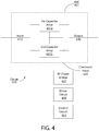
EVC Capacitor Arrays
FIG. 4 shows an electronic circuit 650 for providing a variable capacitance according to one embodiment. The circuit 650 utilizes an EVC 651 that includes two capacitor arrays 651 a, 651 b. The first capacitor array 651 a has a first plurality of discrete capacitors, each having a first capacitance value. The second capacitor array 651 b has a second plurality of discrete capacitors, each having a second capacitance value. The first capacitance value is different from the second capacitance value such that the EVC 651 can provide coarse and fine control of the capacitance produced by the EVC 651. The first capacitor array and the second capacitor array are coupled in parallel between a signal input 613 and a signal output 630.
The first and second capacitance values can be any values sufficient to provide the desired overall capacitance values for the EVC 651. In one embodiment, the second capacitance value is less than or equal to one-half (½) of the first capacitance value. In another embodiment, the second capacitance value is less than or equal to one-third (⅓) of the first capacitance value. In yet another embodiment, the second capacitance value is less than or equal to one-fourth (¼) of the first capacitance value.
The electronic circuit 650 further includes a control circuit 645, which can have features similar to control circuit 45 discussed above. The control circuit 645 is operably coupled to the first capacitor array 651 a and to the second capacitor array 651 b by a command input 629, the command input 629 being operably coupled to the first capacitor array 651 a and to the second capacitor array 651 b. In the exemplified embodiment, the command input 629 has a direct electrical connection to the capacitor arrays 651 a, 651 b, though in other embodiments this connection can be indirect. The coupling of the control circuit 645 to the capacitor arrays 651 a, 651 b will be discussed in further detail below.
The control circuit 645 is configured to alter the variable capacitance of the EVC 651 by controlling on and off states of (a) each discrete capacitor of the first plurality of discrete capacitors and (b) each discrete capacitor of the second plurality of discrete capacitors. As stated above, the control circuit 645 can have features similar to those described with respect to control circuit 45 of FIGS. 2-3. For example, the control circuit 645 can receive inputs from the capacitor arrays 651 a, 651 b, make calculations to determine changes to capacitor arrays 651 a, 651 b, and delivers commands to the capacitor arrays 651 a, 651 b for altering the capacitance of the EVC 651. EVC 651 of FIG. 4 can include a plurality of electronic switches. Each electronic switch can be configured to activate and deactivate one or more discrete capacitors.
As with the control circuit 45 of FIGS. 2-3, the control circuit 645 can also be connected to a driver circuit 639 and an RF choke and filter circuit 637. The control circuit 645, driver circuit 639, and RF choke and filter circuit 637 can have capabilities similar to those discussed with regard to FIG. 2-3. In the exemplified embodiment, the driver circuit 639 is operatively coupled between the control circuit 645 and the first and second capacitor arrays 651 a, 651 b. The driver circuit 639 is configured to alter the variable capacitance based upon a control signal received from the control circuit 645. The RF filter 637 is operatively coupled between the driver circuit 639 and the first and second capacitor arrays 651 a, 651 b. In response to the control signal sent by the control unit 645, the driver circuit 639 and RF filter 637 are configured to send a command signal to the command input 629. The command signal is configured to alter the variable capacitance by instructing at least one of the electronic switches to activate or deactivate (a) at least one the discrete capacitors of the first plurality of discrete capacitors or (b) at least one of the discrete capacitors of the second plurality of discrete capacitors.
In the exemplified embodiment, the driver circuit 639 is configured to switch a high voltage source on or off in less than 15 μsec, the high voltage source controlling the electronic switches of each of the first and second capacitor arrays for purposes of altering the variable capacitance. The EVC 651, however, can be switched by any of the means or speeds discussed in the present application.
The control circuit 645 can be configured to calculate coarse and fine capacitance values to be provided by the respective capacitor arrays 651 a, 651 b. In the exemplified embodiment, the control circuit 645 is configured to calculate a coarse capacitance value to be provided by controlling the on and off states of the first capacitor array 651 a. Further, the control circuit is configured to calculate a fine capacitance value to be provided by controlling the on and off states of the second capacitor array 651 b. In other embodiments, the capacitor arrays 651 a, 651 b can provide alternative levels of capacitance. In other embodiments, the EVC can utilize additional capacitor arrays.
EVC 651 of FIG. 4 can be used in most systems requiring a varying capacitance. For example, EVC 651 can be used as the series EVC and/or shunt EVC in matching network 11 of FIG. 2, or as one or both of the shunt EVCs in matching network 11A of FIG. 3. It is often desired that the differences between the capacitance values allow for both a sufficiently fine resolution of the overall capacitance of the circuit and a wide range of capacitance values to enable a better impedance match at the input of a RF matching network, and EVC 651 allows this.
EVC 651 can also be used in a system or method for fabricating a semiconductor, a method for controlling a variable capacitance, and/or a method of controlling an RF impedance matching network. Such methods can include altering at least one of the series variable capacitance and the shunt variable capacitance to the determined series capacitance value and the shunt capacitance value, respectively. This altering can be accomplishing by controlling, for each of the series EVC and the shunt EVC, on and off states of each discrete capacitor of each plurality of discrete capacitors. In other embodiments, EVC 651 and circuit 650 can be used in other methods and systems to provide a variable capacitance.
Switching In and Out Discrete Capacitors to Vary EVC Capacitance
As discussed above, an EVC is a type of variable capacitor that can use multiple switches, each used to create an open or short circuit, with individual series capacitors to change the capacitance of the variable capacitor. The switches can be mechanical (such as relays) or solid state (such as PIN diodes, transistors, or other switching devices). The following is a discussion of methods for setting up an EVC or other variable capacitor to provide varying capacitances.
In what is sometimes referred to as an “accumulative setup” of an EVC or other variable capacitor, the approach to linearly increase the capacitor value from the minimum starting point (where all switches are open) is to incrementally increase the number of fine tune capacitors that are switched into the circuit. Once the maximum number of fine tune capacitors is switched into circuit, a coarse tune capacitor is switched in, and the fine tune capacitors are switched out. The process starts over with increasing the number of fine tune capacitors that are switched into circuit, until all fine and coarse tune capacitors are switched in, at which point another coarse tune capacitor is switched in and the fine tune capacitors are switched out. This process can continue until all the coarse and fine capacitors are switched in.
In this embodiment, all of the fine tune capacitors have the same or a substantially similar value, and all the coarse tune capacitors have the same or a substantially similar value. Further, the capacitance value of one coarse tune capacitor about equals the combined capacitance value of all fine tune capacitors plus an additional fine tune capacitor into the circuit, thus enabling a linear increase in capacitance. The embodiments, however, are not so limited. The fine tune capacitors (and coarse capacitors) need not have the same or a substantially similar value. Further, the capacitance value of one coarse tune capacitor need not equal the combined capacitance value of all fine tune capacitors plus an additional fine tune capacitor. In one embodiment, the coarse capacitance value and the fine capacitance value have a ratio substantially similar to 10:1. In another embodiment, the second capacitance value is less than or equal to one-half (½) of the first capacitance value. In another embodiment, the second capacitance value is less than or equal to one-third (⅓) of the first capacitance value. In yet another embodiment, the second capacitance value is less than or equal to one-fourth (¼) of the first capacitance value.
An example of the aforementioned embodiment in an ideal setting would be if the fine tune capacitors were equal to 1 pF, and the coarse tune capacitors were equal to 10 pF. In this ideal setup, when all switches are open, the capacitance is equal to 0 pF. When the first switch is closed, there is 1 pF in the circuit. When the second switch is closed there is 2 pF in the circuit, and so on, until nine fine tune switches are closed, giving 9 pF. Then, the first 10 pF capacitor is switched into circuit and the nine fine tune switches are opened, giving a total capacitance of 10 pF. The fine tune capacitors are then switched into circuit from 11 pF to 19 pF. Another coarse tune capacitor can then be switched into circuit and all fine tune capacitors can be switched out of circuit giving 20 pF. This process can be repeated until the desired capacitance is reached.
This can also be taken one step further. Using the previous example, having nine 1 pF capacitors and also nine 10 pF capacitors, the variable capacitor circuit can have even larger values, 100 pF, to switch in and out of circuit. This would allow the previous capacitor array to go up to 99 pF, and then the 100 pF capacitor can be used for the next increment. This can be repeated further using larger increments, and can also be used with any counting system. According to the accumulative setup, increasing the total capacitance of a variable capacitor is achieved by switching in more of the coarse capacitors or more of the fine capacitors than are already switched in without switching out a coarse capacitor that is already switched in. Further, when the variable total capacitance is increased and the control circuit does not switch in more of the coarse capacitors than are already switched in, then the control circuit switches in more fine capacitors than are already switched in without switching out a fine capacitor that is already switched in.
FIG. 5 is a schematic of a variable capacitance system 655 according to an accumulative setup. Where this figure uses reference numbers identical to those of FIG. 4, it is understood that the relevant components can have features similar to those discussed in FIG. 4. The variable capacitance system 655 comprises a variable capacitor 651 for providing a varying capacitance. The variable capacitor 651 has an input 613 and an output 630. The variable capacitor 651 includes a plurality of discrete capacitors 653 operably coupled in parallel. The plurality of capacitors 653 includes first (fine) capacitors 651 a and second (coarse) capacitors 651B. Further, the variable capacitor 651 includes a plurality of switches 661. Of the switches 661, one switch is operably coupled in series to each of the plurality of capacitors to switch in and out each capacitor, thereby enabling the variable capacitor 651 to provide varying total capacitances. The variable capacitor 651 has a variable total capacitance that is increased when discrete capacitors 653 are switched in and decreased when the discrete capacitors 653 are switched out.
The switches 661 can be coupled to switch driver circuits 639 for driving the switches on and off. The variable capacitance system 655 can further include a control unit 645 operably coupled to the variable capacitor 651. Specifically, the control unit 645 can be operably coupled to the driver circuits 639 for instructing the driver circuits 639 to switch one or more of the switches 661, and thereby turn one or more of the capacitors 653 on or off. In one embodiment, the control unit 645 can form part of a control unit that controls a variable capacitor, such as a control unit that instructs the variable capacitors of a matching network to change capacitances to achieve an impedance match. The driver circuits 639 and control unit 645 can have features similar to those discussed above with reference to FIG. 4, and thus can also utilize an RF choke and filter as discussed above.
In one embodiment, the control circuit 645 is configured to determine a desired coarse capacitance for the coarse capacitors; determine a desired fine capacitance for the fine capacitors; and after calculating the desired coarse capacitance and the desired fine capacitance, alter the total variable capacitance by switching in or out at least one of the fine capacitors; and switching in or out at least one of the coarse capacitors. In other embodiments, coarse tuning and fine tuning can occur at different stages.
In the exemplified embodiment, the first capacitors 651 a are fine capacitors each having a capacitance value substantially similar to a fine capacitance value, and the second capacitors 651 b are coarse capacitors each having a capacitance value substantially similar to a coarse capacitance value, the coarse capacitance value being greater than the fine capacitance value. For purposes of this application, capacitances and other values are considered to be substantially similar if one value is not 15 percent (15%) greater than or less than another value.
The variable capacitance system 655 can form part of an impedance matching network, including but not limited to, the impedance matching networks of FIGS. 1-3. The variable capacitance system can also form part of a method for controlling an impedance matching network (such as the impedance matching networks of FIGS. 1-3). The method can include providing the RF impedance matching network comprising determining an increased total capacitance to be provided by one of the EVCs; and increasing the variable total capacitance of the one EVC by switching in more of the coarse capacitors or more of the fine capacitors than are already switched in without switching out a coarse capacitor that is already switched in. Further, the variable capacitance system can form part of a method and system for fabricating a semiconductor (see FIGS. 1-3).
Using the variable capacitance system discussed above with an impedance matching network can provide several advantages over other approaches. An alternative to the above approach would be to have all the capacitor values be different, with the first value equal to the minimum desired change in capacitance. Then each successive capacitor value is increased to double the change in capacitance from the previous up until the maximum desired capacitor value, when all capacitors are switched in. This approach can result in using less capacitors to switch in and out of circuit to achieve the same resolution and range. A potential problem with this setup, however, is that, once the capacitor reaches a certain value, the voltage and/or current on that particular capacitor or the current on the switch can be higher than the specification allows for. This forces the EVC to use multiple capacitors in parallel for each switch of lower value. This problem is particularly acute where high voltages and/or currents are being used. The accumulative setup discussed above avoids putting this degree of stress on its capacitors and switches by switching in additional capacitors, rather than replacing lower-capacitance capacitors with higher-capacitance capacitors.
Determining Capacitance Values to Achieve Match
FIG. 6 is a flow chart showing a process 500A for matching an impedance according to one embodiment. The matching network can include components similar to those discussed above. In one embodiment, the matching network of FIG. 2 is utilized. In the first step of the exemplified process 500A of FIG. 6, an input impedance at the RF input 13 is determined (step 501A). The input impedance is based on the RF input parameter detected by the RF input sensor 21 at the RF input 13. The RF input sensor 21 can be any sensor configured to detect an RF input parameter at the RF input 13. The input parameter can be any parameter measurable at the RF input 13, including a voltage, a current, or a phase at the RF input 13. In the exemplified embodiment, the RF input sensor 21 detects the voltage, current, and phase at the RF input 13 of the matching network 11. Based on the RF input parameter detected by the RF input sensor 21, the control circuit 45 determines the input impedance.
Next, the control circuit 45 determines the plasma impedance presented by the plasma chamber 19 (step 502A). In one embodiment, the plasma impedance determination is based on the input impedance (determined in step 501A), the capacitance of the series EVC 31, and the capacitance of the shunt EVC 33. In other embodiments, the plasma impedance determination can be made using the output sensor 49 operably coupled to the RF output, the RF output sensor 49 configured to detect an RF output parameter. The RF output parameter can be any parameter measurable at the RF output 17, including a voltage, a current, or a phase at the RF output 17. The RF output sensor 49 may detect the output parameter at the RF output 17 of the matching network 11. Based on the RF output parameter detected by the RF output sensor 21, the control circuit 45 may determine the plasma impedance. In yet other embodiments, the plasma impedance determination can be based on both the RF output parameter and the RF input parameter.
Once the variable impedance of the plasma chamber 19 is known, the control circuit 45 can determine the changes to make to the variable capacitances of one or both of the series and shunt EVCs 31, 33 for purposes of achieving an impedance match. Specifically, the control circuit 45 determines a first capacitance value for the series variable capacitance and a second capacitance value for the shunt variable capacitance (step 503A). These values represent the new capacitance values for the series EVC 31 and shunt EVC 33 to enable an impedance match, or at least a substantial impedance match. In the exemplified embodiment, the determination of the first and second capacitance values is based on the variable plasma impedance (determined in step 502A) and the fixed RF source impedance.
Once the first and second capacitance values are determined, the control circuit 45 generates a control signal to alter at least one of the series variable capacitance and the shunt variable capacitance to the first capacitance value and the second capacitance value, respectively (step 504A). This is done at approximately t=−5 μsec. The control signal instructs the switching circuit to alter the variable capacitance of one or both of the series and shunt EVCs 31, 33.
This alteration of the EVCs 31, 33 takes about 9-11 μsec total, as compared to about 1-2 sec of time for an RF matching network using VVCs. Once the switch to the different variable capacitances is complete, there is a period of latency as the additional discrete capacitors that make up the EVCs join the circuit and charge. This part of the match tune process takes about 55 μsec. Finally, the RF power profile 403 is shown decreasing, at just before t=56 μsec, from about 380 mV peak-to-peak to about 100 mV peak-to-peak. This decrease in the RF power profile 403 represents the decrease in the reflected power 407, and it takes place over a time period of about 10 μsec, at which point the match tune process is considered complete.
The altering of the series variable capacitance and the shunt variable capacitance can comprise sending a control signal to the series driver circuit 39 and the shunt driver circuit 43 to control the series variable capacitance and the shunt variable capacitance, respectively, where the series driver circuit 39 is operatively coupled to the series EVC 31, and the shunt driver circuit 43 is operatively coupled to the shunt EVC 43. When the EVCs 31, 33 are switched to their desired capacitance values, the input impedance may match the fixed RF source impedance (e.g., 50 Ohms), thus resulting in an impedance match. If, due to fluctuations in the plasma impedance, a sufficient impedance match does not result, the process of 500A may be repeated one or more times to achieve an impedance match, or at least a substantial impedance match.
Using an RF matching network 11, such as that shown in FIG. 2, the input impedance can be represented as follows:
Z in = ( Z P + Z L + Z series ) Z shunt Z P + Z L + Z series + Z shunt
where Zin is the input impedance, ZP is the plasma impedance, ZL is the series inductor impedance, Zseries is the series EVC impedance, and Zshunt is the shunt EVC impedance. In the exemplified embodiment, the input impedance (Zin) is determined using the RF input sensor 21. The EVC impedances (Zseries and Zshunt) are known at any given time by the control circuitry, since the control circuitry is used to command the various discrete capacitors of each of the series and shunt EVCs to turn ON or OFF. Further, the series inductor impedance (ZL) is a fixed value. Thus, the system can use these values to solve for the plasma impedance (ZP).
Based on this determined plasma impedance (ZP) and the known desired input impedance (Z′in) (which is typically 50 Ohms), and the known series inductor impedance (ZL), the system can determine a new series EVC impedance (Z′series) and shunt EVC impedance (Z′shunt).
Z in = ( Z P + Z L + Z series ) Z shunt Z P + Z L + Z series + Z shunt
Based on the newly calculated series EVC variable impedance (Z′series) and shunt EVC variable impedance (Z′shunt), the system can then determine the new capacitance value (first capacitance value) for the series variable capacitance and a new capacitance value (second capacitance value) for the shunt variable capacitance. When these new capacitance values are used with the series EVC 31 and the shunt EVC 33, respectively, an impedance match may be accomplished.
The exemplified method of computing the desired first and second capacitance values and reaching those values in one step is significantly faster than moving the two EVCs step-by-step to bring either the error signals to zero, or to bring the reflected power/reflection coefficient to a minimum. In semiconductor plasma processing, where a faster tuning scheme is desired, this approach provides a significant improvement in matching network tune speed.
Determining Capacitance Values Using Parameter Matrix
FIG. 7 provides an alternative process 500 for matching an impedance that uses a parameter matrix. In the exemplified process, the control circuit 45 (see FIG. 2 for matching network components) is configured and/or programmed to carry out each of the steps. As one of two initial steps, RF parameters are measured at the RF input 13 by the RF input sensor 21, and the input impedance at the RF input 13 is calculated (step 501) using the measured RF parameters. For this exemplified process 500, the forward voltage and the forward current are measured at the RF input 13. In certain other embodiments, the RF parameters may be measured at the RF output 17 by the RF output sensor 49, although in such embodiments, different calculations may be required than those described below. In still other embodiments, RF parameters may be measured at both the RF input 13 and the RF output 17.
The impedance matching circuit, coupled between the RF source 15 and the plasma chamber 19, may be characterized by one of several types of parameter matrices known to those of skill in the art, including two-port parameter matrices. An S-parameter matrix and a Z-parameter matrix are two examples of such parameter matrices. Other examples include, but are not limited to, a Y-parameter matrix, a G-parameter matrix, an H-parameter matrix, a T-parameter matrix, and an ABCD-parameter matrix. Those of skill in the art will recognize also that these various parameter matrices may be mathematically converted from one to the other for an electrical circuit such as a matching network. The second initial step of the exemplified process 500 is to look up (step 502) the parameter matrix for the existing configuration of the impedance matching circuit in a parameter lookup table. The existing configuration of the impedance matching circuit is defined by existing operational parameters of the impedance matching circuit, particularly the existing array configurations for both of the series EVC 31 and the shunt EVC 33. In order to achieve an impedance match, the existing configuration of the impedance matching circuit is altered to a new configuration of the impedance matching circuit as part of the exemplified process 500.
The parameter lookup table includes a plurality of parameter matrices, with each parameter matrix being associated with a particular configuration of the series EVC 31 and the shunt EVC 33. The parameter lookup table may include one or more of the aforementioned types of parameter matrices. In the exemplified process 500, the parameter lookup table includes at least a plurality of S-parameter matrices. In certain embodiments, the parameter lookup table may include at least a plurality of Z-parameter matrices. In embodiments in which the parameter lookup table includes multiple types of parameter matrices, the different types of parameter matrices are associated within the parameter lookup table in such a way so as to eliminate the need for mathematical conversions between the different types of parameter matrices. For example, the T-parameter matrix may be included as part of the parameter lookup table, with each T-parameter matrix associated with the associated S-parameter matrix that would result from conversion between the two matrices.
The input impedance calculation (step 501) and the parameter matrix look up (step 502) may be performed in any order. With the input impedance calculated (step 501) and the parameter matrix for the existing configuration of the impedance matching circuit identified within the parameter lookup table (step 502) done, the plasma or load impedance may then be calculated (step 503) using the calculated input impedance and the parameter matrix for the existing configuration. Next, from the calculated plasma impedance, the match configurations for the series EVC 31 and the shunt EVC 33 that would achieve an impedance match, or at least a substantial impedance match, between the RF source 15 and the plasma chamber 19 are looked up (step 504) in an array configuration lookup table. These match configurations from the array configuration lookup table are the array configurations which will result in new capacitance values for the series EVC 31 and shunt EVC 33, with an impedance match being achieved with the new array configurations and associated new capacitance values. The array configuration lookup table is a table of array configurations for the series EVC 31 and the shunt EVC 33, and it includes each possible array configuration of the series EVC 31 and the shunt EVC 33 when used in combination. As an alternative to using an array configuration lookup table, the actual capacitance values for the EVCs 31, 33 may be calculated during the process—however, such real-time calculations of the capacitance values are inherently slower than looking up the match configurations in the array configuration lookup table. After the match configurations for the series EVC 31 and the shunt EVC 33 are identified in the array configuration lookup table, then one or both of the series array configuration and the shunt array configuration are altered (step 505) to the respective identified match configurations for the series EVC 31 and the shunt EVC 33.
The altering (step 505) of the series array configuration and the shunt array configuration may include the control circuit 45 sending a control signal to the series driver circuit 39 and the shunt driver circuit 43 to control the series array configuration and the shunt array configuration, respectively, where the series driver circuit 39 is operatively coupled to the series EVC 31, and the shunt driver circuit 43 is operatively coupled to the shunt EVC 43. When the EVCs 31, 33 are switched to the match configurations, the input impedance may match the fixed RF source impedance (e.g., 50 Ohms), thus resulting in an impedance match. If, due to fluctuations in the plasma impedance, a sufficient impedance match does not result, the process of 500 may be repeated one or more times to achieve an impedance match, or at least a substantial impedance match.
The lookup tables used in the process described above are compiled in advance of the RF matching network being used in conjunction with the plasma chamber 19. In creating the lookup tables, the RF matching network 11 is tested to determine at least one parameter matrix of each type and the load impedance associated with each array configuration of the series EVC 31 and the shunt EVC 33 prior to use with a plasma chamber. The parameter matrices resulting from the testing are compiled into the parameter lookup table so that at least one parameter matrix of each type is associated with a respective array configuration of the EVCs 31, 33. Similarly, the load impedances are compiled into the array configuration lookup table so that each parameter matrix is associated with a respective array configuration of the EVCs 31, 33. The pre-compiled lookup tables may take into consideration the fixed RF source impedance (e.g., 50 Ohms), the power output of the RF source, and the operational frequency of the RF source, among other factors that are relevant to the operation of the RF matching network. Each lookup table may therefore have tens of thousands of entries, or more, to account for all the possible configurations of the EVCs 31, 33. The number of possible configurations is primarily determined by how many discrete capacitors make up each of the EVCs 31, 33. In compiling the lookup tables, consideration may be given to possible safety limitations, such as maximum allowed voltages and currents at critical locations inside the matching network, and this may serve to exclude entries in one or more of the lookup tables for certain configurations of the EVCs 31, 33.
As is known in the art, the S-parameter matrix is composed of components called scatter parameters, or S-parameters for short. An S-parameter matrix for the impedance matching circuit has four S-parameters, namely S11, S12, S21, and S22, each of which represents a ratio of voltages at the RF input 13 and the RF output 17. All four of the S-parameters for the impedance matching circuit are determined and/or calculated in advance, so that the full S-parameter matrix is known. The parameters of the other types of parameter matrices may be similarly determined and/or calculated in advance and incorporated into the parameter matrix. For example, a Z-parameter matrix for the impedance matching circuit has four Z-parameters, namely Z11, Z12, Z21, and Z22.
By compiling the parameter lookup table in this manner, the entire time cost of certain calculations occurs during the testing phase for the RF matching network, and not during actual use of the RF matching network 11 with a plasma chamber 19. Moreover, because locating a value in a lookup table can take less time than calculating that same value in real time, using the lookup table can aid in reducing the overall time needed to achieve an impedance match. In a plasma deposition or etching process which includes potentially hundreds or thousands of impedance matching adjustments throughout the process, this time savings can help add directly to cost savings for the overall fabrication process.
From the beginning of the match tune process, which starts with the control circuit determining the variable impedance of the plasma chamber and determining the series and shunt match configurations, to the end of the match tune process, when the RF power reflected back toward the RF source decreases, the entire match tune process of the RF impedance matching network using EVCs has an elapsed time of approximately 110 μsec, or on the order of about 150 μsec or less. This short elapsed time period for a single iteration of the match tune process represents a significant increase over a VVC matching network. Moreover, because of this short elapsed time period for a single iteration of the match tune process, the RF impedance matching network using EVCs may iteratively perform the match tune process, repeating the two determining steps and the generating another control signal for further alterations to the array configurations of one or both of the electronically variable capacitors. By iteratively repeating the match tune process, it is anticipated that a better impedance match may be created within about 2-4 iterations of the match tune process. Moreover, depending upon the time it takes for each repetition of the match tune process, it is anticipated that 3-4 iterations may be performed in 500 μsec or less. Given the 1-2 sec match time for a single iteration of a match tune process for RF impedance matching networks using VVCs, this ability to perform multiple iterations in a fraction of the time represents a significant advantage for RF impedance matching networks using EVCs.
Those of skill in the art will recognize that several factors may contribute to the sub-millisecond elapsed time of the impedance matching process for an RF impedance matching network using EVCs. Such factors may include the power of the RF signal, the configuration and design of the EVCs, the type of matching network being used, and the type and configuration of the driver circuit being used. Other factors not listed may also contribute to the overall elapsed time of the impedance matching process. Thus, it is expected that the entire match tune process for an RF impedance matching network having EVCs should take no more than about 500 μsec to complete from the beginning of the process (i.e., measuring by the control circuit and calculating adjustments needed to create the impedance match) to the end of the process (the point in time when the efficiency of RF power coupled into the plasma chamber is increased due to an impedance match and a reduction of the reflected power). Even at a match tune process on the order of 500 μsec, this process time still represents a significant improvement over RF impedance matching networks using VVCs.
Table 1 presents data showing a comparison between operational parameters of one example of an EVC versus one example of a VVC. As can be seen, EVCs present several advantages, in addition to enabling fast switching for an RF impedance matching network:
TABLE 1
Typical 1000 pF
Parameter EVC Vacuum Capacitors
Capacitance 20 pF~1400 pF  15 pF~1000 pF
Reliability High Low
Response Time ~500 μsec 1 s~2 s
ESR ~13 mW ~20 mW
Voltage 7 kV 5 kV
Current Handling Capability 216 A rms 80 A rms
Volume 4.5 in3 75 in3
As is seen, in addition to the fast switching capabilities made possible by the EVC, EVCs also introduce a reliability advantage, a current handling advantage, and a size advantage. Additional advantages of the RF impedance matching network using EVCs and/or the switching circuit itself for the EVCs include:
    • The disclosed RF impedance matching network does not include any moving parts, so the likelihood of a mechanical failure reduced to that of other entirely electrical circuits which may be used as part of the semiconductor fabrication process. For example, the typical EVC may be formed from a rugged ceramic substrate with copper metallization to form the discrete capacitors. The elimination of moving parts also increases the resistance to breakdown due to thermal fluctuations during use.
    • The EVC has a compact size as compared to a VVC, so that the reduced weight and volume may save valuable space within a fabrication facility.
    • The design of the EVC introduces an increased ability to customize the RF matching network for specific design needs of a particular application. EVCs may be configured with custom capacitance ranges, one example of which is a non-linear capacitance range. Such custom capacitance ranges can provide better impedance matching for a wider range of processes. As another example, a custom capacitance range may provide more resolution in certain areas of impedance matching. A custom capacitance range may also enable generation of higher ignition voltages for easier plasma strikes.
    • The short match tune process (˜500 μsec or less) allows the RF impedance matching network to better keep up with plasma changes within the fabrication process, thereby increasing plasma stability and resulting in more controlled power to the fabrication process.
    • The use of EVCs, which are digitally controlled, non-mechanical devices, in an RF impedance matching network provides greater opportunity to fine tune control algorithms through programming.
    • EVCs exhibit superior low frequency (kHz) performance as compared to VVCs.
      Altering Frequency of RF Source to Fine Tune Match
FIG. 8 is a flow chart showing a process 600 for matching an impedance according to another embodiment. Since EVCs can provide only discretized capacitance values, a matching network that varies only EVCs to create an impedance match can only match based on these discretized values. For example, if a plasma impedance occurs such that the series and/or shunt capacitance values needed to bring the input impedance of the matching network to a desired non-reactive 50 Ohms lies in-between the discretized values, the EVC-based matching network will not be able to tune the input impedance of the matching network to the non-reactive 50 Ohms. The process 600 of FIG. 8 addresses such a circumstance by also altering a frequency of the RF source (sometimes referred to as the “RF generator”) to carry out the impedance match.
The RF source, matching network, and plasma chamber of process 600 can be configured similarly to the system of FIG. 2. Accordingly, reference will be made to the components of the system of FIG. 2, though this figure represents just one embodiment of the invention.
As with previously discussed embodiments, the matching network 11 of process 600 can include an RF input 13 configured to receive an RF signal from an RF source 15, and an RF output 17 configured to operably couple to a plasma chamber 19. The matching network can further include at least one EVC 31, 33, and a control circuit 45 for instructing the at least one EVC 31, 33 to alter its variable capacitance. The RF source 15 (including its control circuitry) and the RF matching network 11 can be in the same enclosure or separate enclosures.
In the process 600, the matching network 11 is initially in an auto tuning mode (step 601). In this mode, the matching network 11 can be configured to carry out automated tuning by altering at least one capacitance value in a manner similar to that described in the foregoing embodiments. In this mode, the process 600 performs tuning referred to as primary tuning (step 602). In the exemplified embodiment, the primary tuning includes altering the series and/or shunt capacitance values in an attempt to achieve an impedance match. In the exemplified embodiment, the desired input impedance (the desired impedance at the input of the matching network 11) is a fixed, non-reactive 50 Ohm, sometimes referred to as the RF source impedance. In other embodiments, the desired input impedance can be any other impedance value, and can be variable.
In the exemplified embodiment, the primary tuning will bring the input impedance relatively close to a non-reactive 50 Ohms, the matching network 11 being limited by the discretized capacitance values of the EVCs 31, 33. At this stage, a preliminary match is achieved (step 603). The preliminary match state will have an associated first reflection parameter value at the RF source output 15 a (the RF source output 15 a being connected to the matching network input 13). In the exemplified embodiment, the first reflection parameter value is a reflected power value. In other embodiments, the first reflection parameter value can be any reflection-related parameter associated with the preliminary match state. For example, the first reflection parameter value can be the reflection coefficient, which represents the ratio of the amplitude of the reflected wave to the incident wave, and is sometimes referred to as gamma. The first reflection parameter can be measured by sensor 21 at the RF source output 15 a. In other embodiments, reflected power can be measured by a sensor or comparable device that is located proximate to the matching network input 13.
In one embodiment, the alteration of variable capacitance in auto tuning mode can include the steps of adjusting the variable capacitance, determining an intermediate reflection parameter value, and then reducing and/or increasing the variable capacitance based on the intermediate reflection parameter value. This process can be repeated such that there are several intermediate reflection parameter values, the adjustment of the one or more variable capacitances being based on these intermediate reflection parameter values. In other embodiments, the invention can omit the use of intermediate reflection parameter values.
Once the preliminary match state is achieved, the matching network 11 can provide a control signal to the RF source 15 indicating that primary tuning is complete and that a preliminary match has been achieved (step 604). The control signal can be any signal sufficient to provide indication that the preliminary match has been achieved.
In response, the RF source 15 can send a hold signal to the matching network 11 (step 605), the hold signal placing the matching network 11 in a manual tuning mode (step 606). In manual tuning mode, the matching network 11 will stop performing automated tuning (and therefore will not alter the variable capacitances) as long as the hold signal is present. In other embodiments, the matching network 11 can automatically enter manual tuning mode when the preliminary match has been achieved, and can return to auto tuning mode when receiving an instruction from the RF source 15.
Next, the variable frequency of the RF source 15 can be adjusted to perform secondary tuning (step 607). This secondary tuning can fine tune the input impedance of the matching network 1 to the desired non-reactive 50 Ohm, or other desired impedance, and can minimize the reflected power at the output of the RF source 15, thereby also decreasing the reflection coefficient. The RF source 15 can have standard control circuitry by which the frequency is varied and the signals discussed above are sent, received, and processed. The frequency can be altered by providing a command to a frequency generation circuit that forms part of the RF source, such as a Direct Digital Synthesizer.
Once the RF source 15 has completed altering the frequency for the secondary tuning, a final match state is achieved (step 608). The final match state will have an associated second reflection parameter value at the RF source output 15 a. As with the first reflection parameter value, in the exemplified embodiment, the second reflection parameter value is a reflected power value. In other embodiments, the second reflection parameter value can be any reflection-related parameter associated with the preliminary match state, such as the reflection coefficient (discussed above). The second reflection parameter can be measured by a sensor 21 at the RF source output 15 a. Since the final match state causes a more finely tuned match than the preliminary match state, the second reflection parameter value will be less than the first reflection parameter value.
The alteration of the variable RF source frequency can include reducing and/or increasing the variable RF source frequency based on an intermediate reflection parameter value. In one embodiment, the alteration of the variable source frequency includes reducing the variable RF source frequency by a first amount and determining the intermediate reflection parameter value at the RF source output. If the intermediate reflection parameter value decreases, the variable RF source frequency is again reduced by the first amount and a new intermediate reflection parameter value is measured. This process can repeat until the intermediate reflection parameter value increases. When the intermediate reflection parameter value increases, the variable source frequency can be increased by a second amount (the second amount being less than the first amount), and then a new intermediate reflection parameter value is determined. If the new intermediate reflection parameter value decreases, the variable source frequency is again increased by the second amount, and a new intermediate reflection parameter value is determined. This process can repeat until the new intermediate reflection parameter value increases or is zero, at which stage the process can stop or the variable source frequency can be returned to its previous value.
The invention is not limited to any one embodiment for tuning the frequency or variable capacitance. For example, the invention can use any variety of methods to step up and/or down the frequency in different increments based on the resulting reflected power. Further, the process 600 can have a minimum reflected parameter value (e.g., a minimum reflected power or minimum reflection coefficient). When the minimum reflected parameter value is achieved, the tuning can stop, regardless of whether the process is in primary or secondary tuning.
Returning to the exemplified embodiment, once the final match state is achieved, the RF source 15 can send a signal (sometimes referred to as a “resume signal”) to the matching network 11 to place the matching network 11 back into auto tuning mode (step 609). The matching network 11 can then be ready for the next variation of the plasma impedance. Thus, when a plasma impedance of the plasma chamber 15 changes, the control circuit 45 can repeat the instruction to alter the variable capacitance and/or the instruction to alter the variable RF source frequency.
In other embodiments, the process 600 will not resume tuning until the reflection parameter value exceeds a predetermined value. Such a tuning restart threshold can be applied to the primary tuning, the secondary tuning, or both. Further, thresholds can be set such that, for small reflected power level raises, only secondary tuning is done (altering the RF source frequency), while, for larger reflected power levels, primary tuning is first carried out (altering capacitances), followed by secondary tuning (altering the RF source frequency).
Combining an EVC-based RF matching network with a variable frequency RF source provides several advantages for fast and precise RF matching. For example, with all components being electronic, the system has higher reliability than those using VVC technology, which are prone to mechanical failures. Further, the primary and second tuning can be performed quickly to enable matching within 500 μsec. Further, the combined EVC matching network and variable RF source can decrease the reflected power to the RF source to essentially 0 Watts.
Restricted Capacitor Switching
The matching networks discussed above can alter their variable capacitance values to achieve an impedance match. This process is sometimes referred to as tuning. The state of the impedance matching can be assessed based on a reflection parameter value. In the exemplified embodiments, the reflection parameter value is a reflected power value. More specifically, the reflection parameter value is a reflection coefficient value (sometimes referred to as “gamma”), which represents the ratio of the amplitude of a reflected wave to an incident wave. Referring to the system 85 of FIG. 2, the reflection parameter value can be measured by sensor 21 at the matching network input 13 (or RF source 15 output), or by sensor 49 at the matching network output 17 (or plasma chamber 19 input). Such a sensor can provide a signal to the control circuit 45 indicative of the reflection parameter value. In other embodiments, the reflection parameter value can be any reflection-related parameter associated with a match state.
In one approach to achieving an impedance match, a matching algorithm requires the control loop of the RF matching network to continue to tune until the reflection coefficient value at the input of the matching network is reduced below a certain level. This level is sometimes referred to as “gamma-stop.” If the load impedance changes, the reflection coefficient at the input of the RF matching network can increase. If this reflection coefficient increases beyond a certain reflection coefficient value, sometimes referred to as “gamma-restart,” then the RF matching network starts to tune again. In a solid-state RF matching network, there are typically no restrictions on how many switches can switch ON or OFF at any time, therefore based on the change in the reflection coefficient, the number of switches switching at any time can be significant and thus can result in perturbing the plasma to make it unstable.
In an alternative approach, an intermediate gamma value is utilized such that there are three gamma values: (1) a first reflection value (gamma-stop) at which tuning is stopped, (2) a second reflection value (gamma-restart-low) at which capacitor switching is limited, and (3) a third reflection value (gamma-restart-high) at which capacitor switching is unlimited.
FIG. 9 is flow chart showing a process for matching an impedance where capacitor switching can be restricted using the above reflection values. In the exemplified embodiment, the reflection coefficient value is continuously monitored (operation 202). When the match is tuned and the reflection coefficient value (gamma) is not above the first reflection value (operation 204), no capacitors switch (operation 210). When the reflection coefficient value goes above the second reflection value (but is at or below the third reflection value) (operation 206), only a predetermined number of predetermined fine capacitors can switch at this time (restricted tune) (operation 212). Whether to turn these switches ON or OFF will depend upon what was the actual calculated position of the capacitors. When the reflection coefficient value goes above the third reflection value (operation 208), the capacitors can switch without any restrictions (unrestricted tune) (operation 214). For the purpose of this description, the fine capacitors can be any capacitors that are used to provide finer capacitance movement steps than the coarse capacitors. In one embodiment, the coarse capacitors have a capacitance at least twice as large as the capacitance of the fine capacitors.
In one example, the predetermined number is two (only two capacitors can switch when the reflection coefficient value initially exceeds the second reflection value), and the three reflection values are as follows: (1) first reflection value (gamma-stop)=0.031, (2) second reflection value (gamma-restart-low)=0.07, (3) third reflection value (gamma-restart-high)=0.10. In this example, the matched position is C4F5/C6F7 (i.e., 4 coarse capacitor switches ON and 5 fine capacitor switches ON for one solid state capacitor array, and 6 coarse capacitor switches ON and 7 fine capacitor switches ON for the second solid state capacitor array), and this positioning is determined before determining how to switch the discrete capacitors.
If the reflection coefficient value is calculated as 0.08, and the new tuned position is calculated to be C3F0/C7F1, then the match will go to C4F3/C6F9, rather than going directly to C3F0/C7F1. The control circuit can continuously monitor the reflection coefficient value (or other reflection parameter), and thus this loop can run as many times as needed until either the reflection coefficient value goes below the first reflection value or the reflection coefficient value goes above the third reflection value. If the reflection coefficient value goes above the third reflection value (i.e., 0.10), then the capacitor switches are not restricted and can directly switch to the calculated position. Note that the foregoing capacitor restrictions can also be applied to when the match is moving from a higher reflection coefficient value to a lower reflection coefficient value to provide a slower settling profile. Not also, while the embodiment described above discusses altering the tuning based on whether a reflection parameter is above, or at, or below a reflection parameter (or some combination thereof), other embodiments can use any one of these options (or a combination of options) provided different values are used as reference values for determining what type of tuning to use. For example, in one embodiment the system can carry out an unrestricted tune when the reflection parameter is above the third reflection value, while in another embodiment the system can carry out an unrestricted tune when the reflection parameter is at or above the third reflection value.
By the above multi-step reflection value approach, if something changes in the process that changes the impedance by a significant amount, then the match can respond faster, but if the change is small, then the match will not take big steps to cause the plasma to become unstable. This restricted capacitor switching approach can be used, for example, with the matching networks discussed above. A control circuit, such as control circuit 45 or 645 can be used to carry out the steps of determining or receiving the reflection parameter value and controlling the altering of the discrete capacitors based on that value. It is further noted that the restricted capacitor approach described above can be used in conjunction with the other impedance matching and capacitor-switching methods discussed herein. Further, the restricted capacitor switching approach can be used with a matching network that forms part of a semiconductor processing tool, such as that shown in FIGS. 1-3. Further, the restricted capacitor switching approach can be used with a matching network as part of a method of manufacturing a semiconductor.
Matching Using EVC and Frequency
In yet another embodiment, impedance matching can be carried out using an EVC and frequency considerations. According to one embodiment, a single EVC is used. For example, in FIG. 3, capacitor 33A can be an EVC, while capacitor 31A can be non-variable. (In other embodiments, more than one capacitor in the matching network can be variable.) The matching network can be calibrated such that post-calibration, at least one of the lookup tables (such as the lookup tables discussed above) contains information to provide the best combination of capacitor position and frequency for a load impedance to get the lowest input reflected power or input reflection coefficient (input gamma).
During operation, in one embodiment the matching network determines the input impedance based on the information provided by an input RF sensor, such as a VI (voltage-current) sensor located at the RF input of the matching network. The matching network then uses this input impedance information and the current EVC configuration (e.g., capacitor switch positions) and the frequency information to calculate the plasma chamber (load) impedance. Alternatively, rather than calculating the load impedance from input impedance and the calibration parameters of the match, the load impedance can be directly measured from an output sensor at the RF output of the matching network.
In the next step of this embodiment, the matching network uses the determined load impedance and the match lookup table to determine the new EVC configuration and the new frequency that would provide the lowest reflected power or lowest input reflection coefficient at the RF input for enabling an impedance match. Such an approach provides a much faster means for tuning compared to linearly changing the capacitor switch positions and frequency based on the polarity and magnitude of the input error signal.
When the matching network is coupled to a plasma chamber and operating, the RF source (e.g., an RF generator) or the customer's system can provide the matching network with the frequency signal through some communication port (e.g., analog). Alternately, the matching network can detect the frequency at its RF input port. Based on this specific frequency, the matching network can use the lookup table to determine what EVC configuration, for that frequency, provides the lowest input reflected power or input reflection coefficient (gamma) for enabling an impedance match. The matching network's control circuit can then choose this EVC position and command the discrete switches of the EVC to switch the EVC to this new configuration providing a new capacitance.
In another embodiment, the matching network can determine the best EVC configuration and frequency combination to provide the lowest input reflected power or input reflection coefficient (gamma). The matching network's control circuit can then move the EVC to the new configuration (e.g., desired switch positions) and at the same time command the RF generator to move to the desired frequency. For example, this method can use EVC technology for the EVC and frequency tuning for the other leg and make an ‘L’ or ‘pi’ type of match for higher power operation, up to 6 or 10 kW.
Returning to FIG. 3, this semiconductor processing system 85A can be understood as carrying out one or more of the embodiments discussed above. The matching network 11A has an input 13 coupled to an RF source 15 having a variable frequency, and an output coupled to a plasma chamber 19 having a variable chamber impedance. The matching network 11A further includes two capacitors, where capacitor 33A may be an EVC and capacitor 31A may be non-variable. The matching network 11A has a control circuit 45 coupled to at least one of sensors 21 and sensor 49, the one or more sensors configured to detect an RF parameter. The control circuit may use a match lookup table (such as one of the lookup tables discussed above) with a value based on the detected RF parameter to determine a match combination. The match combination includes both a new EVC configuration for providing a new EVC capacitance, and a new source frequency for the RF source. Once these determinations have been made, the control circuit 45 can alter the EVC 33A to the new EVC configuration (and thus provide a new capacitance) and alter the variable frequency of the RF source to the new source frequency.
In other embodiments, the match combination may instead be only a new EVC configuration, where the lookup table bases this configuration on the current frequency being provided by the RF source. In such an embodiment, the RF source may be controlled by a separate second control circuit 16.
In the exemplified embodiment, the value based on the detected RF parameter (used with the match lookup table) is the variable chamber impedance. In other embodiments, the RF parameter can be any RF parameter associated with the matching network or processing system. For example, the RF parameter may be detected at the RF input 13 (by sensor 21) or at the RF output 17 (by sensor 49). In some embodiments, the value based on the detected RF parameter can be the detected RF parameter itself.
In the exemplified embodiment, the EVC comprises discrete capacitors having different configurations defining ON and OFF states of the discrete capacitors, these different configurations causing the EVC to provide different capacitances. For example, each discrete capacitor may have a corresponding switch to activate or deactivate the discrete capacitor, the EVC being altered to a new EVC configuration by the switches activating or deactivating at least one of the discrete capacitors of the EVC. The corresponding switch may be in series with or parallel to the discrete capacitor.
In one embodiment, prior to an impedance match, the EVC has a first configuration defining ON and OFF states of the discrete capacitors, and the variable frequency of the RF source has a first frequency. The control circuit determines, based on the detected RF parameter, an input impedance at the RF input of the matching network. The control circuit then determines the variable chamber impedance from a parameter matrix lookup table using (1) the determined input impedance of the impedance matching network; (2) the first configuration of the EVC; and (3) the first frequency of the RF source. The control circuit then uses the determined variable chamber impedance with the match lookup table to determine the match combination. The sensor may be a voltage and current sensor positioned at the RF input of the matching network. Further, the parameter matrix lookup table may include two-port parameter matrices, such as S-parameter matrices or Z-parameter matrices.
In another embodiment, the RF sensor 21 is a phase or magnitude detector operably coupled to the RF input 13 of the matching network 11A, and the detected RF parameter used for the determination of the match combination is a phase error or a magnitude error. In another embodiment, the RF sensor is operably coupled to the RF input of the matching network, and the detected RF parameter is at least one of a voltage, a current, or a phase at the RF input. Further, the determination of the match combination may use the match lookup table with a reflection coefficient based on the at least one of the voltage, the current, or the phase, the reflection coefficient being the value based on the detected RF parameter. In yet another embodiment, the RF sensor 49 is operably coupled to the RF output 17 of the matching network, and the determination of the match combination uses the match lookup table with a load impedance based on the RF parameter detected by the RF sensor at the RF output.
FIG. 10 is a flow chart showing an embodiment of a process 110 for matching an impedance using a lookup table to alter an EVC configuration and an RF source frequency. In a first step, the sensor detects an RF parameter (step 112). To cause an impedance match between the RF source and the plasma chamber, the control circuit determines, using a match lookup table with value based on the detected RF parameter, a match combination of a new EVC configuration for providing a new EVC capacitance, and a new source frequency for the RF source (step 114). The control circuit then alters the EVC to the new EVC configuration, and alters the variable frequency of the RF source to the new source frequency (step 116).
The above process may be carried out as part of a method of manufacturing a semiconductor. Such a manufacturing method may include placing a substrate in the plasma chamber configured to deposit a material layer onto the substrate or etch a material layer from the substrate; and energizing plasma within the plasma chamber by coupling RF power from the RF source into the plasma chamber to perform a deposition or etching. Further, the matching network described above may form part of a semiconductor processing tool (such as tool 86 in FIG. 3), the tool including the plasma chamber 19 and the matching network 11A.
Matching Using Independent EVC and Frequency Control
In yet another embodiment, impedance matching can be carried out using an EVC and frequency considerations where the EVC and the frequency are controlled separately. According to one embodiment, a single EVC is used. For example, in FIG. 3, capacitor 33A can be an EVC, while capacitor 31A can be non-variable. In other embodiments, more than one capacitor in the matching network can be variable, or capacitor 31A can be eliminated. The matching network can be calibrated such that post-calibration, at least one of the lookup tables (such as the lookup tables discussed above) contains information to provide the best capacitor positions for a load impedance to have the lowest input reflected power or input reflection coefficient (input gamma).
During operation, the matching network can determine the input impedance by those methods described above with respect to FIG. 10, such as by using a VI (voltage-current) sensor located at the RF input of the matching network. Also similar to the embodiments discussed above, the matching network can use the input impedance information and the current EVC configuration (e.g., capacitor switch positions) and the frequency information to calculate a load impedance. Alternatively, rather than calculating the load impedance from input impedance and the calibration parameters of the match, the load impedance can be directly measured from an output sensor at the RF output of the matching network. In the exemplified embodiment, the load impedance to be calculated or otherwise determined is the impedance at the EVC output (see, e.g., EVC output 41B of FIG. 12). In certain embodiments, this load impedance is the variable chamber impedance and the impedance of the frequency-sensitive circuit (see frequency-sensitive circuit 37B of FIG. 12), though the invention to a particular load impedance.
Similar to the embodiments related to FIG. 10, the matching network can use the determined load impedance and the match lookup table to determine a new EVC configuration to provide a lower reflected power or input reflection coefficient at the RF input for helping enable an impedance match. Unlike the embodiment of FIG. 10, however, the new frequency provided by the RF source is determined independently of the determination of the new EVC configuration.
Returning to FIG. 3, the semiconductor processing system 85A can be understood as carrying out one or more of the embodiments discussed above. The matching network 11A has an input 13 coupled to an RF source 15 having a variable frequency, and an output coupled to a plasma chamber 19 having a variable chamber impedance. The matching network 11A further includes two capacitors, where capacitor 33A may be an EVC and capacitor 31A may be non-variable. The matching network 11A has a first control circuit 45 coupled to at least one of sensors 21 and sensor 49, the one or more sensors configured to detect an RF parameter. The control first circuit 45 may use a match lookup table (such as one of the lookup tables discussed above) with a value based on the detected RF parameter to determine a new EVC configuration for providing a new EVC capacitance. Once these determinations have been made, the first control circuit 45 can alter the EVC 33A to the new EVC configuration and thereby assist in causing an impedance match between the RF source and the plasma chamber. In one embodiment, this altering of the EVC configuration can be understood as one step towards causing an impedance match (the change in frequency being a different and separate step). In these embodiments, the first control circuit 45 controlling the EVC is separate and distinct from a second control circuit 16 for controlling the frequency of the RF source.
In the exemplified embodiment, the second control circuit 16 alters the variable frequency of the RF source 15, independently from the first control circuit, to further cause the impedance match between the RF source and the plasma chamber. In one embodiment, this frequency altering can be understood as a second (and possibly final) step in causing an impedance match, though the time of occurrence of the two steps may to some extent overlap. The first control circuit 45 does not provide instructions to the second control circuit 16 for controlling the variable frequency of the RF source 15. The second control circuit's frequency alteration occurs independently from the first control circuit.
In certain embodiments, the second control circuit can form part of the RF source. In other embodiments, the second control circuit can form part of the matching network. In yet other embodiments, the second control circuit can be distinct from both the RF source and the matching network.
In the exemplified embodiment, the value based on the detected RF parameter (used with the match lookup table) is the load impedance (e.g., the impedance at the EVC 33A output). In other embodiments, the RF parameter can be any RF parameter associated with the matching network or processing system. For example, the RF parameter may be detected at the RF input 13 (by sensor 21) or at the RF output 17 (by sensor 49). In some embodiments, the value based on the detected RF parameter can be the detected RF parameter itself. As with earlier embodiments, the EVC comprises discrete capacitors having different configurations defining ON and OFF states of the discrete capacitors, these different configurations causing the EVC to provide different capacitances.
In one embodiment, prior to an impedance match, the EVC has a first configuration defining ON and OFF states of the discrete capacitors. The first control circuit determines, based on the detected RF parameter, an input impedance at the RF input of the matching network. The control circuit then determines the load impedance from a parameter matrix lookup table using (1) the determined input impedance of the impedance matching network; and (2) the first configuration of the EVC. The control circuit then uses the determined load impedance with the match lookup table to determine the new EVC configuration. The sensor may be a voltage and current sensor positioned at the RF input of the matching network. Further, the parameter matrix lookup table may include two-port parameter matrices, such as S-parameter matrices or Z-parameter matrices. Further, the RF sensor may have any of the characteristic discussed above with regard to the previous embodiments, and the determination of the EVC configuration may use the match lookup table with a reflection coefficient.
FIG. 11 is a flow chart showing an embodiment of a process 120 for matching an impedance where capacitance and frequency are adjusted independently. The process 120 includes an EVC subprocess 121 and a frequency subprocess 125 operating in parallel and independently. For the EVC subprocess 121, in a first step the sensor detects an RF parameter (step 122). To assist in causing an impedance match between the RF source and the plasma chamber, the first control circuit determines, using a match lookup table with value based on the detected RF parameter, a new EVC configuration for providing a new EVC capacitance (step 123). The first control circuit then alters the EVC to the new EVC configuration (step 124).
For the frequency subprocess 125, in a first step the second control circuit determines an RF parameter. In one embodiment, the RF parameter is a reflected power or reflection coefficient at the RF source output, though the invention is not so limited. In a second step, the second control circuit alters an RF source frequency based on the determined RF parameter.
The above process may be carried out as part of a method of manufacturing a semiconductor. Such a manufacturing method may include placing a substrate in the plasma chamber configured to deposit a material layer onto the substrate or etch a material layer from the substrate; and energizing plasma within the plasma chamber by coupling RF power from the RF source into the plasma chamber to perform a deposition or etching. Further, the matching network described above may form part of a semiconductor processing tool (such as tool 86 in FIG. 3), the tool including the plasma chamber 19 and the matching network 11A.
FIG. 12 is a schematic of an embodiment of a matching network 11B having a frequency-sensitive circuit 37B responsive to frequency adjustments. The frequency-sensitive circuit is designed to have an impedance that can vary significantly when the variable frequency of the RF source is altered. In the exemplified embodiment, the frequency-sensitive circuit 37B includes an LC circuit 38B having a capacitor 34B and an inductor 35B. The frequency-sensitive circuit 37B can further include series capacitor 36B. In one embodiment, the variable chamber impedance can provide an inductance or capacitance for the LC circuit. The matching network 11B includes an input 13B and an output 17B. It further includes an EVC 33B having an EVC output 41B. A second capacitor 39B can also be included. This capacitor can be, for example, an EVC, a variable capacitor that is not an EVC (e.g., a vacuum variable capacitor), or a non-variable capacitor. As discussed, the determination of the new EVC configuration can use a match lookup table with a load impedance, and the load impedance in certain embodiments can be an impedance at an output 41B of the EVC, the EVC output impedance being the value based on the detected RF parameter. Further, the EVC output impedance can be the variable chamber impedance and the impedance of the frequency-sensitive circuit forming part of the impedance matching network.
The exemplified embodiment of FIG. 11 addresses the issue that the matching network may not be able control the frequency of the RF source. Further, communications between the match and generator may be slow, so they may not be able to send the frequency information fast enough for fast tuning. The current invention is based on the discovery that the matching network can match without knowledge of the frequency, or any frequency tuning being carried out by the generator. The matching network can view the frequency tuning elements as part of the load. Simulations were run to confirm the results, as well as testing units on static loads.
Simulations
Two tests were run, one on a 400 kHz variable matching network and the other on a 13.56 MHz variable matching network. The matching circuits were altered by adding capacitors around the inductor in both parallel and in series, as can be seen in FIG. 12. The frequency range for the 400 kHz unit is 360 kHz to 440 kHz, ±10%, and the shunt capacitor varies from 200 pF to 38,960 pF. For the 13.56 MHz unit, the frequency range is 12.88 MHz to 14.24 MHz, ±5%, and the capacitor range of 290 pF to 1910 pF. These are simplified models, as not all ESRs and other parasitics are accounted for.
As the frequency sweeps, the parallel capacitor gives the inductor a higher impedance at one end of the spectrum, while the series capacitor gives a lower inductance at the other end of the spectrum. In the case of the 13.56 MHz match, the circuit resonates and has a capacitive impedance at one end of the spectrum. This is what gives the frequency tuning its impedance variability on the imaginary axis.
The two matching circuits were then tested to verify that they were able to match fixed loads, and as a reference for later testing. This was done manually by varying the capacitor, and then the frequency. These two steps were then repeated until the VSWR was below an acceptable level, which was 1.1:1. The 400 kHz matched a load impedance of 45-j372, with a capacitance of approximately 12,197 and frequency of 416.9 kHz with a VSWR of 1.03:1. The 13.56 MHz unit also tuned into a fixed load with a frequency of 13.99 MHz and capacitance of about 425 pF.
The next set of testing assumed that the matching network neither has control of the generator, or any knowledge of the frequency. There are multiple reasons why this could be the case, as stated above. The first step was to remove the frequency-sensitive portion of the match. This leaves only the variable capacitor. This was done using a circuit similar to matching network 11B of FIG. 12, but where frequency-sensitive portion 37B and capacitor 39B are eliminated. The next step was to simulate and measure the two-port network parameters. FIG. 13 is a portion of a Smith chart 128 showing the simulation for fifteen different capacitor values 129 measured at 13.56 MHz, and their response 130 over frequency. It is shown that, as the frequency shifts, the impedance shifts towards the nearest point, filling in the arc.
This was noteworthy, because it indicates that the change in impedance caused by an increase or decrease in percentage of capacitance is equivalent to the change in impedance due to an increase or decrease in percentage of frequency, as one would expect in view of Equation 1 below.
X c = 1 2 π Δ % freq C = 1 2 π freq Δ % C
Further, one could say that this is similar to adding or removing a shunt capacitor in parallel to the variable capacitor. The capacitor in parallel with the variable capacitor could be considered part of the load, as it is attached to the same node.
Thus, it can be assumed for a one-dimensional match that the change in capacitance due to frequency is equivalent to a change in the load, having a capacitor at the input shunt leg. When running in auto-tune mode, the match would see this change in frequency as a change in the load. Thus, if the load changes by a certain percentage due to frequency, the variable capacitor would adjust by a proportionate difference but in the opposite sign to counteract the change in impedance.
The next step was to look at the matching algorithm and how it would react to changes in frequency. To do this, the one-dimensional match circuit was simulated at three different frequencies, 13.56 MHz and at ±5%, and with 169 different capacitor values ranging from 290 pF to 1910 pF. The Z-Parameters were calculated for each combination, and then the best matching capacitance table was generated by inputting a different load impedance with each set of Z-Parameters and finding which position had the lowest gamma for each load at each frequency.
The next step was to use a list of various input impedances and the Z-Parameters to calculate different load impedances for each frequency at different capacitor positions. For example, when the variable capacitor is at 50%, and the input impedance is determined to be 20+j0Ω, the load impedance for each frequency can be calculated. These calculated load impedances are then used to find the best match position on the lookup table.
Since the V/I sensor has little change when the frequency is swept, we can assume the input impedance reading would not be affected by it changing. The V/I sensor also assumes that the frequency is 13.56 MHz. To measure the accuracy of the match over frequency, the best match capacitor percentage will be compared to the other two frequencies finding their perspective best matches for their calculated loads. So, at 50% capacitance and an input impedance of 20+j0Ω, the 13 MHz match will have a load of 4.9+j10.3Ω, the 12.88 MHz will have a load of 5.5+10.6Ω, and the 14.24 MHz will have a load of 4.4+j10.0Ω. Multiple input impedances were randomly picked and their data can be found below in Table 2.
TABLE 2
Frequency versus Best Match Capacitor Position
Capacitor
Input Start Capacitor End Position
Impedance Position 12.88 MHz 13.56 MHz 14.24 MHz
20 + j0 25.0% 11.3% 11.9% 11.9%
20 + j0 50.0% 36.3% 36.9% 36.9%
20 + j0 75.0% 61.9% 61.9% 61.9%
 50 + j50 25.0% 36.3% 35.7% 35.7%
 50 + j50 50.0% 61.3% 60.7% 60.1%
 50 + j50 75.0% 86.3% 85.1% 85.1%
 50 − j50 25.0% 20.8% 21.4% 21.4%
 50 − j50 50.0% 45.8% 46.4% 47.0%
 50 − j50 75.0% 70.8% 72.0% 72.0%
200 + j0  25.0% 28.6% 28.6% 29.2%
200 + j0  50.0% 54.2% 54.2% 54.2%
200 + j0  75.0% 80.4% 79.8% 79.2%
As it can be seen in Table 2, the best match positions are extremely close to one another across frequency. The major source of error is from quantization, where the load impedances were calculated to the nearest 0.1Ω for the lookup table, and there are only 169 different capacitor positions.
Testing was done with both the 400 kHz unit and the 13.56 MHz unit. The S-parameters were measured and the best match table was calculated for specified load impedance ranges. The unit was set to automatically change the capacitor position while the frequency was varied manually. For the 400 kHz unit, the load was again set to 45-j372Ω. The matched condition was at frequency 417 kHz, 100 Hz higher than the manually tuned test, and a capacitance of approximately 12,428 pF, one fine cap position more than in the manually tuned test, giving a VSWR of 1.04:1. The 13.56 MHz match was also tuned to its load. The matched condition was at frequency 13.98 MHz, which was 10 kHz less than the manually tuned test, and the capacitance was about 435 pF, one fine position higher than the manually tuned test. This gave a VSWR of 1.07:1.
It was concluded that a one-dimensional EVC match with variable frequency sweep tuning was capable of working. With the input V/I sensor and two-port network parameters, the change in impedance due to frequency was equivalent to a load with a change in an input shunt capacitor. The tuning tables show that the variable capacitor's value will be the same at different frequencies for a given input impedance. The testing showed that the algorithm works with a manually adjusted frequency.
Matching with Multi-Level Power Setpoints
In modern semiconductor processes, there are instances where the process requires the RF source to generate a multi-level pulse signal such that the RF signal has cyclically recurring pulse intervals with differing amplitude levels. In some cases, the change in the power setpoint amplitude level can be very frequent and of the order of a few tens of hundreds of microseconds. The multi-level power setpoint can be two levels or more. Such pulsing is sometimes referred to as level-to-level pulsing because the power setpoint goes from one level to another and not just between a level and zero. While such cyclic adjustment of the intensity level of the RF energy used to generate the plasma can provide advantages, it also creates challenges with regard to impedance matching, due to the rapid variations in the load impedance caused by the differing pulse levels.
Typical RF matching networks based on electromechanical components, such as vacuum variable capacitors, cannot move their positions for the short pulses of level-to-level pulsing, and therefore they are set to (or their internal automatic matching algorithms set themselves to) an average position for the electromechanical components setting. This is not an optimal method, since the electromechanical matching network is not tuned to either one level or the other and thus the RF source in the system is exposed to high reflected power for each of the levels.
An RF matching network utilizing solid state technology, which may include the use of EVCs, is able to tune significantly faster, and thus is able to match for each of the power setpoint levels. The methods described below provide methods for performing RF impedance matching when the RF signal has multi-level power setpoints. The methods can be applied to various types of RF matching networks based on solid state technology, including as those matching networks discussed above that utilize one or more EVCs.
FIGS. 14 and 15 are discussed below to describe an embodiment for performing level-to-level pulsing. In the exemplified embodiment, two non-zero pulse levels are utilized. The invention is not so limited, however, as any number of two or more pulse levels may be used. Further, the exemplified embodiment measures the parameters voltage, current, and phase at the RF input, and generates running parameter-related values (described below) based on these values, but the invention can measure any parameter (one or more) related to the load, and make that measurement at other locations in the system (e.g., the RF output of the matching network), and base the parameter-related values on any of those different parameters.
FIG. 14 provides a flow chart of the exemplified process 300 for impedance matching when the RF input signal has multi-level power setpoints. FIG. 15 provides a graph 330 of RF signal 332 having a first pulse level L1 and second pulse level L2, as well as the times 338, 339 for determining the parameter-related value. In the exemplified embodiment, the pulse level changes periodically at a pulse level interval 333, 334.
Returning to FIG. 14, the control circuit of the matching network detects whether the first pulse level is being provided (operation 302). If so, the control circuit measures the parameter related to the load for the first pulse level (operation 304), which in this embodiment includes the voltage (V), current (I), and phase (Φ) at the input of the matching network (see parameters 336 in FIG. 15). These values can be measured independent of the RF source, or the system can synchronize sampling with when the RF source samples them. Based on the measured parameter, the control circuit will determine a parameter-related value for the first pulse level (operation 306), which will be used to alter the EVC (operation 308), provided the control unit determines that an alteration to the EVC is warranted.
The parameter-related value can be any value based on the one or more measured parameters. In its simplest form, the parameter-related value may be the measured parameter(s) itself. In the exemplified embodiment, however, the parameter-related value is based on previously-determined parameter-related values. Specifically, the new parameter-related value is an average of the current measured parameter and a predetermined number of previously-determined parameter-related values. For example, at the last time of times 338, the parameter-related value is the average of the parameter value at the last time of times 338 (the current time) and the parameter-related values determined at the first three times of times 338 (the previous three times). In other embodiments, other methods of using prior parameter-related value(s) may be used.
In the exemplified embodiment, the parameter-related value is used to calculate the input impedance at the RF input of the matching network (Zinput low). In other embodiments, other values can be determined, such as the reflection coefficient at the RF input of the matching network (Γinput low). The exemplified system uses the calculated input impedance (Zinput low) (or related value such as Γinput low) and the matching network's parameter matrix (such as one of the parameter matrices discussed above) to determine the load impedance (Zoutput low). The system next uses the determined load impedance along with the desired input impedance at the input of the match (typically 50+j0) to determine the best configuration for the EVCs of the matching network—that is, to determine the best positions for the discrete capacitors of the EVCs (EVC1low1 and EVC2low2). In the exemplified embodiment, the matching network uses two EVCs, though in other embodiments more or less EVCs can be used. In another embodiment, the system could alter one or more EVCs in conjunction with altering an RF frequency, thus using a combination of capacitor tuning and frequency tuning. In this embodiment, the system will determine both the best EVC configuration and the best RF frequency value (e.g., EVC1low1 and freqlow1). In the exemplified embodiment, the matching network next changes the EVCs to their new configurations. Accordingly, EVC1 is changed to the EVC1low1 position, and EVC2 is changed to the EVC2low2 position. In other embodiments, other configurations may be used, such as changing to EVC1low1 and freqlow1. Note that the invention is not limited to the method for determining a match impedance discussed above. One or more of these steps may be omitted between determining the parameter-related value and the match configuration, and/or be substituted with another step for ultimately determining the new match configuration. For example, while the foregoing embodiments performed matching based on input impedance or a reflection coefficient, in other embodiments matching can be performed based on alternative values, such as maximum delivered energy during a pulse or minimum loss of energy during a pulse. Further, matching can be based on RF input phase and/or magnitude errors, on the measured reflected power, or on a load impedance measured directly at the output of the matching network.
Note that the system may include certain schemes that limit the extent to which the capacitor positions may be changed at a given time. For example, the alteration of the at least one EVC to provide the match configuration may be prevented from being carried out until a predetermined time has passed since a previous alteration of the at least one EVC. This scheme can ensure sufficient time has passed to allow the previous capacitor change to take effect. Further, in certain circumstances, a protection scheme may allow one of the EVCs to change to a newly determined position, but will not allow the other EVC (or EVCs) to move to a newly determined position (or positions). In other embodiments, the protection scheme may prevent any number of changes to the capacitor positions or frequency. In the exemplified embodiment, the changes that are permitted by the protection scheme will be made, while the other capacitor positions (or RF frequency) will be held at its current position (or frequency).
As shown in FIG. 15, during the first pulse interval 333, the control circuit will measure the parameter at several times 338 and repeat steps 302-308 for each time 338, regularly updating the parameter-related value. In the exemplified embodiment, the times 338 (and times 339) for calculating a new parameter-related value are separated by a time interval 340 that is 4 microseconds. In other embodiments, the time interval 340 can be of a different duration.
During first pulse interval 333, while a first level process 301A is being carried out, an independent second level process 301B is being carried out. While the first pulse level is being detected (operation 302), the second pulse level is not being detected (operation 312). During this first pulse interval 333, while the first level process 301A is measuring the parameter to determine the parameter-related value and alter the EVCs accordingly, second level process 301B is determining a parameter-related value for the second pulse level (operation 320) without measuring the parameter. This can be done by several methods. In the exemplified embodiment, presuming there were prior parameter measurements when the second pulse level L2 was ON, the parameter-related value will be based on a predetermined number of previously-determined parameter-related values. For example, the current parameter-related value may be based on an average of a predetermined number of previously determined parameter-related values. For example, while when the pulse is ON the parameter-related value is the average of the currently measured parameter value and three previously-determined parameter-related values, when the pulse is OFF the parameter-related value is the average of the four previously-determined parameter-related values. Thus, even when a given pulse level is OFF, a new parameter-related value can regularly be generated at each time interval 340. The parameter-related value is not simply a previously measured parameter value being held in memory until the pulse level is turned back ON, but is a value (for each pulse level) being newly determined at regular intervals, even when a given pulse level is OFF, to create a data bus of values.
At second pulse interval 335, the first pulse level L1 is OFF and the second pulse level L2 is ON. When this occurs, the first pulse level L1 and the second pulse level L2 switch roles. For the first pulse level (which is OFF), parameter-related values are determined at times 339 without use of a newly measured parameter (operation 310), similar to the process described with respect to operation 320 of the second-level process. For the second pulse level (which is ON), parameter-related values are determined (operation 316) at times 339 using new parameter measurements (314), and the at least one EVC is altered accordingly (operation 318). The different options for determining the parameter, the parameter-related value, and the match configuration apply to both the first level process 301A and the second level process 301B.
The above-disclosed process for impedance matching during level-to-level pulsing provides several advantages. There is no interruption in collecting parameter-related data, and the data set collected for each power level is practically continuous. As a result, the control loop can access this data at any time for determining new EVC and/or frequency settings. Because in a preferred embodiment this data also relies upon averaging the last few measured values, the disclosed method reduces the noise and sudden measurement changes associated with stopping and starting the measurement process. Further, the disclosed method of determining parameter values for each level, irrespective of whether the level is ON or OFF, allows the control system to treat each level as if it is its own matching network, thus increasing the flexibility and scalability of the control system to multi-level pulsing.
The above process may be carried out as part of a method of manufacturing a semiconductor. Such a manufacturing method may include placing a substrate in the plasma chamber configured to deposit a material layer onto the substrate or etch a material layer from the substrate; and energizing plasma within the plasma chamber by coupling RF power from the RF source into the plasma chamber to perform a deposition or etching. Further, the matching network described above may form part of a semiconductor processing tool (such as tool 86 in FIG. 3), the tool including the plasma chamber 19 and the matching network 11A.
While the embodiments of a matching network discussed herein have used L or pi configurations, it is noted that the claimed matching network may be configured in other matching network configurations, such as a ‘T’ type configuration. Unless stated otherwise, the variable capacitors, switching circuits, and methods discussed herein may be used with any configuration appropriate for an RF impedance matching network.
While the embodiments discussed herein use one or more variable capacitors in a matching network to achieve an impedance match, it is noted that any variable reactance element can be used. A variable reactance element can include one or more discrete reactance elements, where a reactance element is a capacitor or inductor or similar reactive device.
While the inventions have been described with respect to specific examples including presently preferred modes of carrying out the invention, those skilled in the art will appreciate that there are numerous variations and permutations of the above described systems and techniques. It is to be understood that other embodiments may be utilized and structural and functional modifications may be made without departing from the scope of the present inventions. Thus, the spirit and scope of the inventions should be construed broadly as set forth in the appended claims.

Claims (20)

What is claimed is:
1. A method for impedance matching comprising:
positioning a matching network between a radio frequency (RF) source and a load, wherein:
the RF source is configured to provide at least two non-zero pulse levels; and
the matching network comprises at least one electronically variable capacitor (EVC) configured to alter its capacitance to provide a match configuration;
for each of the at least two pulse levels, at a regular time interval, regardless of whether the pulse level is detected, determining a parameter-related value that is based on a parameter related to the load;
repeatedly detecting which of the at least two non-zero pulse levels is being provided by the RF source; and
upon detecting one of the at least two non-zero pulse levels, for the detected pulse level:
measuring the parameter related to the load to determine a measured parameter value;
determining the parameter-related value based on the measured parameter value; and
altering the at least one EVC to provide the match configuration, the match configuration based on the parameter-related value.
2. The method of claim 1 wherein each EVC of the matching network comprises discrete capacitors configured to switch in and out to vary the capacitance of the EVC and thereby provide the match configuration.
3. The method of claim 1 wherein the load is a plasma chamber having a variable impedance.
4. The method of claim 1 wherein the measured parameter value is at least one of a voltage, a current, or a phase at an input of the matching network.
5. The method of claim 1 wherein the determination of the parameter-related value is based on at least one previously-determined parameter-related value.
6. The method of claim 5 wherein the parameter-related value is based on an average of the measured parameter value and the one or more previously-determined parameter values.
7. The method of claim 1 wherein the alteration of the at least one EVC to provide the match configuration is prevented from being carried out until a predetermined time has passed since a previous alteration of the at least one EVC.
8. The method of claim 1 wherein the match configuration is determined based on a load impedance value, which is determined based on an input impedance value at the input of the matching network or a reflection coefficient, which is determined based on the measured parameter value.
9. The method of claim 8 wherein the load impedance value is determined using a parameter matrix.
10. The method of claim 1 wherein the altering of the capacitance of the EVC to provide the match configuration is accompanied by an altering of a frequency provided by the RF source to enable frequency tuning.
11. A matching network comprising:
an RF input operably coupled to an RF source, the RF source configured to provide at least two non-zero pulse levels;
an RF output operably coupled to a load;
at least one electronically variable capacitor (EVC) configured to alter its capacitance to provide a match configuration; and
a control circuit configured to:
for each of the at least two pulse levels, at a regular time interval, regardless of whether the pulse level is detected, determine a parameter-related value that is based on a parameter related to the load;
repeatedly detect which of the at least two non-zero pulse levels is being provided by the RF source; and
upon detecting one of the at least two non-zero pulse levels, for the detected pulse level:
measure the parameter related to the load to determine a measured parameter value;
determine the parameter-related value based on the measured parameter value; and
alter the at least one EVC to provide the match configuration, the match configuration based on the parameter-related value.
12. The matching network of claim 11 wherein each EVC of the matching network comprises discrete capacitors configured to switch in and out to vary the capacitance of the EVC and thereby provide the match configuration.
13. The matching network of claim 11 wherein the load is a plasma chamber having a variable impedance.
14. The matching network of claim 11 wherein the measured parameter value is at least one of a voltage, a current, or a phase at an input of the matching network.
15. The matching network of claim 11 wherein the determination of the parameter-related value is based on at least one previously-determined parameter-related value.
16. The matching network of claim 15 wherein the parameter-related value is based on an average of the measured parameter value and the one or more previously-determined parameter values.
17. The matching network of claim 11 wherein the alteration of the at least one EVC to provide the match configuration is prevented from being carried out until a predetermined time has passed since a previous alteration of the at least one EVC.
18. The matching network of claim 11 wherein the match configuration is determined based on a load impedance value, which is determined based on an input impedance value at the input of the matching network or a reflection coefficient, which is determined based on the measured parameter value.
19. A semiconductor processing tool comprising:
a plasma chamber configured to deposit a material onto a substrate or etch a material from the substrate; and
an impedance matching circuit operably coupled to the plasma chamber, the matching circuit comprising:
an RF input operably coupled to an RF source, the RF source configured to provide at least two non-zero pulse levels;
an RF output operably coupled to the plasma chamber;
at least one electronically variable capacitor (EVC) configured to alter its capacitance to provide a match configuration; and
a control circuit configured to:
for each of the at least two pulse levels, at a regular time interval, regardless of whether the pulse level is detected, determine a parameter-related value that is based on a parameter related to the plasma chamber;
repeatedly detect which of the at least two non-zero pulse levels is being provided by the RF source; and
upon detecting one of the at least two non-zero pulse levels, for the detected pulse level:
measure the parameter related to the plasma chamber to determine a measured parameter value;
determine the parameter-related value based on the measured parameter value; and
alter the at least one EVC to provide the match configuration, the match configuration based on the parameter-related value.
20. A method of manufacturing a semiconductor, the method comprising:
placing a substrate in a plasma chamber configured to deposit a material layer onto the substrate or etch a material layer from the substrate;
coupling an impedance matching circuit between an RF source and the plasma chamber, wherein:
the RF source is configured to provide at least two non-zero pulse levels; and
the matching network comprises at least one electronically variable capacitor (EVC) configured to alter its capacitance to provide a match configuration; and
performing impedance matching by:
for each of the at least two pulse levels, at a regular time interval, regardless of whether the pulse level is detected, determining a parameter-related value that is based on a parameter related to the load;
repeatedly detecting which of the at least two non-zero pulse levels is being provided by the RF source; and
upon detecting one of the at least two non-zero pulse levels, for the detected pulse level:
measuring the parameter related to the load to determine a measured parameter value;
determining the parameter-related value based on the measured parameter value; and
altering the at least one EVC to provide the match configuration, the match configuration based on the parameter-related value.
US16/592,453 2017-07-10 2019-10-03 Impedance matching with multi-level power setpoint Active 2039-01-29 US11114280B2 (en)

Priority Applications (16)

Application Number Priority Date Filing Date Title
US16/592,453 US11114280B2 (en) 2017-07-10 2019-10-03 Impedance matching with multi-level power setpoint
US16/685,698 US11120971B2 (en) 2017-07-10 2019-11-15 Diagnostics for impedance matching network
US16/804,324 US10714314B1 (en) 2017-07-10 2020-02-28 Impedance matching network and method
US16/839,424 US10741364B1 (en) 2017-07-10 2020-04-03 Impedance matching network and method
US16/843,138 US10720309B1 (en) 2017-07-10 2020-04-08 Impedance matching network and method
US16/926,002 US11101110B2 (en) 2017-07-10 2020-07-10 Impedance matching network and method
US16/926,154 US11264210B2 (en) 2017-07-10 2020-07-10 Impedance matching network and method
US16/935,643 US11393659B2 (en) 2017-07-10 2020-07-22 Impedance matching network and method
US16/935,600 US11289307B2 (en) 2017-07-10 2020-07-22 Impedance matching network and method
US17/111,830 US11398370B2 (en) 2017-07-10 2020-12-04 Semiconductor manufacturing using artificial intelligence
US17/111,743 US11476091B2 (en) 2017-07-10 2020-12-04 Impedance matching network for diagnosing plasma chamber
US17/344,327 US11557461B2 (en) 2017-07-10 2021-06-10 Impedance matching network
US17/363,207 US11521833B2 (en) 2017-07-10 2021-06-30 Combined RF generator and RF solid-state matching network
US17/723,702 US20220254610A1 (en) 2017-07-10 2022-04-19 Resonant filter for solid state rf impedance matching network
US17/979,180 US11948775B2 (en) 2017-07-10 2022-11-02 Combined RF generator and RF solid-state matching network
US18/120,591 US20230215696A1 (en) 2017-07-10 2023-03-13 Power control for rf impedance matching network

Applications Claiming Priority (9)

Application Number Priority Date Filing Date Title
US201762530446P 2017-07-10 2017-07-10
US201862693625P 2018-07-03 2018-07-03
US16/029,742 US10483090B2 (en) 2017-07-10 2018-07-09 Restricted capacitor switching
US201862711141P 2018-07-27 2018-07-27
US201862741073P 2018-10-04 2018-10-04
US201862782915P 2018-12-20 2018-12-20
US16/502,656 US11315758B2 (en) 2017-07-10 2019-07-03 Impedance matching using electronically variable capacitance and frequency considerations
US16/524,805 US10727029B2 (en) 2017-07-10 2019-07-29 Impedance matching using independent capacitance and frequency control
US16/592,453 US11114280B2 (en) 2017-07-10 2019-10-03 Impedance matching with multi-level power setpoint

Related Parent Applications (1)

Application Number Title Priority Date Filing Date
US16/524,805 Continuation-In-Part US10727029B2 (en) 2017-07-10 2019-07-29 Impedance matching using independent capacitance and frequency control

Related Child Applications (1)

Application Number Title Priority Date Filing Date
US16/685,698 Continuation-In-Part US11120971B2 (en) 2017-07-10 2019-11-15 Diagnostics for impedance matching network

Publications (2)

Publication Number Publication Date
US20200035461A1 US20200035461A1 (en) 2020-01-30
US11114280B2 true US11114280B2 (en) 2021-09-07

Family

ID=69178286

Family Applications (1)

Application Number Title Priority Date Filing Date
US16/592,453 Active 2039-01-29 US11114280B2 (en) 2017-07-10 2019-10-03 Impedance matching with multi-level power setpoint

Country Status (1)

Country Link
US (1) US11114280B2 (en)

Families Citing this family (12)

* Cited by examiner, † Cited by third party
Publication number Priority date Publication date Assignee Title
JP7094179B2 (en) * 2018-08-28 2022-07-01 東京エレクトロン株式会社 Impedance matching method and impedance matching device
US10816581B2 (en) * 2018-09-17 2020-10-27 Infineon Technologies Ag RF impedance measurement and tuning system
US20220200561A1 (en) * 2019-05-15 2022-06-23 Motomu Matsunaga Impedance matching device
JP7299130B2 (en) 2019-10-11 2023-06-27 株式会社ダイヘン high frequency power circuit
JP7437142B2 (en) 2019-11-25 2024-02-22 株式会社ダイヘン High frequency power system
JP7465657B2 (en) 2019-12-27 2024-04-11 株式会社ダイヘン Impedance Adjustment Device
JP2021108413A (en) 2019-12-27 2021-07-29 株式会社ダイヘン Impedance adjustment device and impedance adjustment method
JP7450387B2 (en) 2019-12-27 2024-03-15 株式会社ダイヘン Impedance adjustment device
JP2021106354A (en) 2019-12-27 2021-07-26 株式会社ダイヘン High frequency power supply system
CN116779407A (en) * 2020-10-13 2023-09-19 北京北方华创微电子装备有限公司 Acquisition method, impedance matcher method and semiconductor process equipment
JP2022067321A (en) * 2020-10-20 2022-05-06 東京エレクトロン株式会社 Plasma generation device, plasma processing device, and plasma processing method
DE102021201937A1 (en) * 2021-03-01 2022-09-01 TRUMPF Hüttinger GmbH + Co. KG Impedance matching method, impedance matching arrangement and plasma system

Citations (144)

* Cited by examiner, † Cited by third party
Publication number Priority date Publication date Assignee Title
US3828281A (en) 1973-02-26 1974-08-06 Lorain Prod Corp Impedance simulating circuit for transmission lines
US4110700A (en) 1977-10-25 1978-08-29 Rca Corporation Electronically tunable microwave frequency FET discriminator
US4679007A (en) 1985-05-20 1987-07-07 Advanced Energy, Inc. Matching circuit for delivering radio frequency electromagnetic energy to a variable impedance load
US4692643A (en) 1983-10-28 1987-09-08 Hitachi, Ltd. Semiconductor switching device having plural MOSFET's, GTO's or the like connected in series
US4751408A (en) 1985-09-06 1988-06-14 Thomson-Csf Voltage-switching device
US4929855A (en) 1988-12-09 1990-05-29 Grumman Corporation High frequency switching device
US5012123A (en) 1989-03-29 1991-04-30 Hittite Microwave, Inc. High-power rf switching system
US5079507A (en) 1989-01-30 1992-01-07 Daihen Corporation Automatic impedance adjusting apparatus for microwave load and automatic impedance adjusting method therefor
US5654679A (en) 1996-06-13 1997-08-05 Rf Power Products, Inc. Apparatus for matching a variable load impedance with an RF power generator impedance
EP0840349A2 (en) 1996-11-04 1998-05-06 Applied Materials, Inc. RF tuning method for an RF plasma reactor using frequency servoing power, voltage, current or dI/dt control
EP0840350A2 (en) 1996-11-04 1998-05-06 Applied Materials, Inc. Plasma apparatus and process with filtering of plasma sheath-generated harmonics
US5815047A (en) 1993-10-29 1998-09-29 Applied Materials, Inc. Fast transition RF impedance matching network for plasma reactor ignition
US5849136A (en) 1991-10-11 1998-12-15 Applied Materials, Inc. High frequency semiconductor wafer processing apparatus and method
US5880921A (en) 1997-04-28 1999-03-09 Rockwell Science Center, Llc Monolithically integrated switched capacitor bank using micro electro mechanical system (MEMS) technology
US5889252A (en) 1996-12-19 1999-03-30 Lam Research Corporation Method of and apparatus for independently controlling electric parameters of an impedance matching network
US5971591A (en) 1997-10-20 1999-10-26 Eni Technologies, Inc. Process detection system for plasma process
US6046641A (en) 1998-07-22 2000-04-04 Eni Technologies, Inc. Parallel HV MOSFET high power stable amplifier
US6137367A (en) 1998-03-24 2000-10-24 Amcom Communications, Inc. High power high impedance microwave devices for power applications
US20020060914A1 (en) 1999-03-23 2002-05-23 Advanced Energy Industries, P.C. High frequency power generator and related methods
US6400012B1 (en) 1997-09-17 2002-06-04 Advanced Energy Voorhees, Inc. Heat sink for use in cooling an integrated circuit
US6424232B1 (en) 1999-11-30 2002-07-23 Advanced Energy's Voorhees Operations Method and apparatus for matching a variable load impedance with an RF power generator impedance
US20030046013A1 (en) 1998-02-27 2003-03-06 Gerrish Kevin S. Voltage current sensor with high matching directivity
US6583572B2 (en) 2001-03-30 2003-06-24 Lam Research Corporation Inductive plasma processor including current sensor for plasma excitation coil
US6621372B2 (en) 2001-03-01 2003-09-16 Daihen Corporation Impedance matching device
US6657395B2 (en) 2000-08-17 2003-12-02 Tokyo Electron Limited Close coupled match structure for RF drive electrode
US6677828B1 (en) 2000-08-17 2004-01-13 Eni Technology, Inc. Method of hot switching a plasma tuner
US6703080B2 (en) 2002-05-20 2004-03-09 Eni Technology, Inc. Method and apparatus for VHF plasma processing with load mismatch reliability and stability
US6791274B1 (en) 2003-07-15 2004-09-14 Advanced Energy Industries, Inc. RF power control device for RF plasma applications
US6794951B2 (en) 2002-08-05 2004-09-21 Veeco Instruments, Inc. Solid state RF power switching network
US6818562B2 (en) 2002-04-19 2004-11-16 Applied Materials Inc Method and apparatus for tuning an RF matching network in a plasma enhanced semiconductor wafer processing system
US6888396B2 (en) 2002-03-11 2005-05-03 California Inst Of Techn Multi-cascode transistors
US6888313B2 (en) 2003-07-16 2005-05-03 Advanced Energy Industries, Inc. Impedance matching network with termination of secondary RF frequencies
US6946847B2 (en) 2002-02-08 2005-09-20 Daihen Corporation Impedance matching device provided with reactance-impedance table
US6967547B2 (en) 2002-06-24 2005-11-22 Signal Technology Corporation RF switch including diodes with intrinsic regions
US7004107B1 (en) 1997-12-01 2006-02-28 Applied Materials Inc. Method and apparatus for monitoring and adjusting chamber impedance
USRE39051E1 (en) 1997-09-15 2006-03-28 Eni Technology, Inc. Fuzzy logic tuning of RF matching network
US7071786B2 (en) 2003-07-09 2006-07-04 Mitsubishi Denki Kabushiki Kaisha Cascode circuit and integrated circuit having it
US20060170367A1 (en) 2005-01-11 2006-08-03 Bhutta Imran A Method of detecting RF power delivered to a load and complex impedance of the load
US7095178B2 (en) 2001-11-27 2006-08-22 Alps Electric Co., Ltd. Plasma processing apparatus, method for operating the same, designing system of matching circuit, and plasma processing method
US20060198077A1 (en) 2005-03-05 2006-09-07 Innovation Engineering Llc Electronically variable capacitor array
US7113761B2 (en) 2003-10-07 2006-09-26 Motorola, Inc. RF power device with on-chip digital control and optical interface
US7122965B2 (en) 2003-02-24 2006-10-17 Mks Instruments, Inc. Methods and apparatus for calibration and metrology for an integrated RF generator system
US20060232471A1 (en) 2005-04-18 2006-10-19 Mks Instruments, Inc. Phase and frequency control of a radio frequency generator from an external source
US7164236B2 (en) 2000-08-08 2007-01-16 Tokyo Electron Limited Method and apparatus for improved plasma processing uniformity
US7199678B2 (en) 2004-11-09 2007-04-03 Daihen Corporation Impedance matching apparatus for a plasma chamber comprising two separate storage units and calculators
US20070075784A1 (en) 2004-02-05 2007-04-05 Ola Pettersson Radio frequency power amplifier
US20070139122A1 (en) 2005-10-31 2007-06-21 Mks Instruments, Inc. Radio Frequency Power Delivery System
US7298091B2 (en) 2002-02-01 2007-11-20 The Regents Of The University Of California Matching network for RF plasma source
US7304438B2 (en) 2003-09-22 2007-12-04 Mks Instruments, Inc. Method and apparatus for preventing instabilities in radio-frequency plasma processing
US20080180179A1 (en) 2007-01-25 2008-07-31 Mks Instruments, Inc. RF Power Amplifier Stability Network
US20080179948A1 (en) 2005-10-31 2008-07-31 Mks Instruments, Inc. Radio frequency power delivery system
US20080197854A1 (en) 2007-02-16 2008-08-21 Mks Instruments, Inc. Harmonic Derived Arc Detector
US7439610B2 (en) 2006-06-16 2008-10-21 M/A-Com, Inc. High power shunt switch with high isolation and ease of assembly
US7480571B2 (en) 2002-03-08 2009-01-20 Lam Research Corporation Apparatus and methods for improving the stability of RF power delivery to a plasma load
US7495524B2 (en) 2006-03-31 2009-02-24 Daihen Corporation Impedance matching apparatus
US7498908B2 (en) 2006-08-04 2009-03-03 Advanced Energy Industries, Inc High-power PIN diode switch
US7514935B2 (en) 2006-09-13 2009-04-07 Advanced Energy Industries, Inc. System and method for managing power supplied to a plasma chamber
US7518466B2 (en) 2005-08-29 2009-04-14 Applied Materials, Inc. Methods and apparatus for symmetrical and/or concentric radio frequency matching networks
US7535312B2 (en) 2006-11-08 2009-05-19 Paratek Microwave, Inc. Adaptive impedance matching apparatus, system and method with improved dynamic range
US20090207537A1 (en) 2008-02-14 2009-08-20 Mks Instruments, Inc. Application Of Wideband Sampling For Arc Detection With A Probabilistic Model For Quantitatively Measuring Arc Events
US20100001796A1 (en) 2008-07-01 2010-01-07 Mks Instruments, Inc. Radio Frequency (RF) Envelope Pulsing Using Phase Switching of Switch-Mode Power Amplifiers
US7666464B2 (en) 2004-10-23 2010-02-23 Applied Materials, Inc. RF measurement feedback control and diagnostics for a plasma immersion ion implantation reactor
US20100073104A1 (en) 2008-09-24 2010-03-25 Mks Instruments, Inc. Tune Range Limiter
US7714676B2 (en) 2006-11-08 2010-05-11 Paratek Microwave, Inc. Adaptive impedance matching apparatus, system and method
US20100123502A1 (en) 2008-07-09 2010-05-20 Bhutta Imran A System for providing a substantially uniform potential profile
US7745955B2 (en) 2005-10-17 2010-06-29 Huettinger Elektronik Gmbh + Co. Kg RF plasma supply device
US7755300B2 (en) 2003-09-22 2010-07-13 Mks Instruments, Inc. Method and apparatus for preventing instabilities in radio-frequency plasma processing
US20100194195A1 (en) 2009-02-05 2010-08-05 Mks Instruments, Inc. Radio Frequency Power Control System
US20100201370A1 (en) 2008-02-14 2010-08-12 Mks Instruments, Inc. Arc Detection
US7868556B2 (en) 2005-08-05 2011-01-11 Advanced Micro-Fabrication Equipment, Inc. Asia RF matching network of a vacuum processing chamber and corresponding configuration methods
US7917104B2 (en) 2007-04-23 2011-03-29 Paratek Microwave, Inc. Techniques for improved adaptive impedance matching
US7969096B2 (en) 2006-12-15 2011-06-28 Mks Instruments, Inc. Inductively-coupled plasma source
US20110241781A1 (en) 2010-04-02 2011-10-06 Mks Instruments, Inc. Variable Class Characteristic Amplifier
US20110247696A1 (en) 2010-04-09 2011-10-13 Advanced Energy Industries, Inc. Mass flow controller with enhanced operating range
US8089026B2 (en) 2003-08-18 2012-01-03 Mks Instruments, Inc. Methods for control of plasma transitions in sputter processing systems using a resonant circuit
US8102954B2 (en) 2005-04-26 2012-01-24 Mks Instruments, Inc. Frequency interference detection and correction
US20120062322A1 (en) 2010-09-09 2012-03-15 Mks Instruments, Inc. Power Amplifier With Transistor Input Mismatching
US8203859B2 (en) 2006-12-29 2012-06-19 Daihen Corporation High frequency device with variable frequency and variable load impedance matching
US8228112B2 (en) 2007-07-13 2012-07-24 International Business Machines Corporation Switch with reduced insertion loss
US20120188007A1 (en) 2011-01-20 2012-07-26 Advanced Energy Industries, Inc. Impedance-Matching Network Using BJT Switches in Variable-Reactance Circuits
US8264154B2 (en) 2008-05-14 2012-09-11 Applied Materials, Inc. Method and apparatus for pulsed plasma processing using a time resolved tuning scheme for RF power delivery
US8278909B2 (en) 2009-07-16 2012-10-02 Mks Instruments, Inc. Wide-dynamic range electrometer with a fast response
US8299867B2 (en) 2006-11-08 2012-10-30 Research In Motion Rf, Inc. Adaptive impedance matching module
US8314561B2 (en) 2010-04-02 2012-11-20 Mks Instruments, Inc. Multi-channel radio frequency generator
US8330432B2 (en) 2009-12-22 2012-12-11 Advanced Energy Industries, Inc Efficient active source impedance modification of a power amplifier
US8335479B2 (en) 2006-11-09 2012-12-18 Renesas Electronics Corporation Semiconductor integrated circuit, RF module using the same, and radio communication terminal device using the same
US8344559B2 (en) 2009-05-05 2013-01-01 Advanced Energy Industries, Inc. Multi-feed RF distribution systems and methods
US8368469B2 (en) 2010-03-10 2013-02-05 Purdue Research Foundation Silicon-on-insulator high power amplifiers
US8368308B2 (en) 2009-03-05 2013-02-05 Applied Materials, Inc. Inductively coupled plasma reactor having RF phase control and methods of use thereof
US20130043854A1 (en) 2011-08-17 2013-02-21 Mks Instruments, Inc. Adjustable resonant buck converter
US8436643B2 (en) 2010-11-04 2013-05-07 Advanced Energy Industries, Inc. High frequency solid state switching for impedance matching
US8461842B2 (en) 2003-07-18 2013-06-11 Mks Instruments, Inc. Methods and systems for stabilizing an amplifier
US20130169359A1 (en) 2011-12-29 2013-07-04 Mks Instruments, Inc. Power Distortion-Based Servo Control Systems For Frequency Tuning RF Power Sources
US8487706B2 (en) 2010-01-25 2013-07-16 Peregrine Semiconductor Corporation Stacked linear power amplifier with capacitor feedback and resistor isolation
US8502689B2 (en) 2010-09-23 2013-08-06 Applied Materials, Inc. System and method for voltage-based plasma excursion detection
US20130207738A1 (en) 2011-11-03 2013-08-15 Advanced Energy Industries, Inc. High frequency solid state switching for impedance matching
US8513889B2 (en) 2009-10-21 2013-08-20 Applied Materials, Inc. Methods and apparatus for tuning matching networks
US20130222055A1 (en) 2012-02-23 2013-08-29 Mks Instruments, Inc. Feedback Control And Coherency Of Multiple Power Supplies In Radio Frequency Power Delivery Systems For Pulsed Mode Schemes in Thin Film Processing
US8536636B2 (en) 2007-04-26 2013-09-17 Peregrine Semiconductor Corporation Tuning capacitance to enhance FET stack voltage withstand
US20130257311A1 (en) 2012-03-27 2013-10-03 Mks Instruments, Inc. Versatile zero-voltage switch resonant inverter for industrial dielectric barrier discharge generator applications
US8552665B2 (en) 2010-08-20 2013-10-08 Advanced Energy Industries, Inc. Proactive arc management of a plasma load
US8559907B2 (en) 2004-06-23 2013-10-15 Peregrine Semiconductor Corporation Integrated RF front end with stacked transistor switch
US8569842B2 (en) 2011-01-07 2013-10-29 Infineon Technologies Austria Ag Semiconductor device arrangement with a first semiconductor device and with a plurality of second semiconductor devices
US8576010B2 (en) 2010-10-19 2013-11-05 Samsung Electronics Co., Ltd. Apparatus and method for a switched capacitor architecture for multi-band doherty power amplifiers
US8587321B2 (en) 2010-09-24 2013-11-19 Applied Materials, Inc. System and method for current-based plasma excursion detection
US20130314163A1 (en) 2012-05-22 2013-11-28 Rf Micro Devices, Inc. Integrated stacked power amplifier and rf switch architecture
US20130320853A1 (en) 2009-02-02 2013-12-05 Advanced Energy Industries, Inc. Passive power distribution for multiple electrode inductive plasma source
US8624501B2 (en) 2010-12-08 2014-01-07 Mks Instruments, Inc. Measuring and controlling parameters of a plasma generator
US20140009248A1 (en) 2012-07-05 2014-01-09 Rf Micro Devices, Inc. Spac series programmable array of capacitors
US8638159B2 (en) 2008-02-28 2014-01-28 Peregrine Semiconductor Corporation Devices and methods for improving voltage handling and/or bi-directionality of stacks of elements when connected between terminals
US20140028398A1 (en) 2012-07-27 2014-01-30 Mks Instruments, Inc. Wideband AFT Power Amplifier Systems With Frequency-Based Output Transformer Impedance Balancing
US20140049250A1 (en) 2012-08-16 2014-02-20 Mks Instruments, Inc. On The Enhancements of Planar Based RF Sensor Technology
US8659335B2 (en) 2009-06-25 2014-02-25 Mks Instruments, Inc. Method and system for controlling radio frequency power
US20140062303A1 (en) 2012-08-28 2014-03-06 Advanced Energy Industries, Inc. Systems and methods for calibrating a switched mode ion energy distribution system
US20140061156A1 (en) 2012-08-28 2014-03-06 Advanced Energy Industries, Inc. Wide dynamic range ion energy bias control; fast ion energy switching; ion energy control and a pulsed bias supply; and a virtual front panel
US8674606B2 (en) 2009-04-27 2014-03-18 Advanced Energy Industries, Inc. Detecting and preventing instabilities in plasma processes
US8680928B2 (en) 2012-03-29 2014-03-25 Avago Technologies General Ip (Singapore) Pte. Ltd. Power amplifier including variable capacitor circuit
US8686796B2 (en) 2011-04-19 2014-04-01 Qualcomm Incorporated RF power amplifiers with improved efficiency and output power
US20140097908A1 (en) 2012-03-23 2014-04-10 Mks Instruments, Inc. System and Methods of Bimodal Automatic Power and Frequency Tuning of RF Generators
US20140117872A1 (en) 2012-11-01 2014-05-01 Advanced Energy Industries, Inc. Adjustable non-dissipative voltage boosting snubber network
US20140117861A1 (en) 2012-11-01 2014-05-01 Advanced Energy Industries, Inc. Differing boost voltages applied to two or more anodeless electrodes for plasma processing
US20140118031A1 (en) 2012-10-30 2014-05-01 Mks Instruments, Inc. RF Pulse Edge Shaping
US8716984B2 (en) 2009-06-29 2014-05-06 Advanced Energy Industries, Inc. Method and apparatus for modifying the sensitivity of an electrical generator to a nonlinear load
US8723423B2 (en) 2011-01-25 2014-05-13 Advanced Energy Industries, Inc. Electrostatic remote plasma source
US8781415B1 (en) 2013-02-07 2014-07-15 Mks Instruments, Inc. Distortion correction based feedforward control systems and methods for radio frequency power sources
US8779859B2 (en) 2012-08-08 2014-07-15 Qualcomm Incorporated Multi-cascode amplifier bias techniques
US20140218076A1 (en) 2013-02-07 2014-08-07 Mks Instruments, Inc. Synchronization of RF Pulsing With RF Metrology, Processing, and Control
US20140231243A1 (en) 2012-11-01 2014-08-21 Advanced Energy Industries, Inc. Charge removal from electrodes in unipolar sputtering system
US8815329B2 (en) 2008-12-05 2014-08-26 Advanced Energy Industries, Inc. Delivered energy compensation during plasma processing
US20140266492A1 (en) 2013-03-15 2014-09-18 Mks Instruments, Inc. Virtual RF Sensor
US8847561B2 (en) 2008-05-07 2014-09-30 Advanced Energy Industries, Inc. Apparatus, system, and method for controlling a matching network based on information characterizing a cable
US20140320013A1 (en) 2013-04-26 2014-10-30 Mks Instruments, Inc. Multiple Radio Frequency Power Supply Control of Frequency and Phase
US8884525B2 (en) 2011-03-22 2014-11-11 Advanced Energy Industries, Inc. Remote plasma source generating a disc-shaped plasma
US8884180B2 (en) 2008-12-05 2014-11-11 Advanced Energy Industries, Inc. Over-voltage protection during arc recovery for plasma-chamber power supplies
US8928329B2 (en) 2011-07-26 2015-01-06 Mks Instruments, Inc. Cold cathode gauge fast response signal circuit
US20150115289A1 (en) 2013-10-30 2015-04-30 United Silicon Carbide, Inc. Hybrid wide-bandgap semiconductor bipolar switches
US9083343B1 (en) 2014-05-28 2015-07-14 United Silicon Carbide, Inc. Cascode switching circuit
US20150200079A1 (en) * 2014-01-10 2015-07-16 Reno Technologies, Inc. Rf impedance matching network
US9190993B1 (en) 2015-01-08 2015-11-17 United Silicon Carbide, Inc. High voltage switch
US9306533B1 (en) 2015-02-20 2016-04-05 Reno Technologies, Inc. RF impedance matching network
US20160134260A1 (en) * 2014-01-10 2016-05-12 Reno Technologies, Inc. Rf impedance matching network
US9496122B1 (en) * 2014-01-10 2016-11-15 Reno Technologies, Inc. Electronically variable capacitor and RF matching network incorporating same
US10269540B1 (en) 2018-01-25 2019-04-23 Advanced Energy Industries, Inc. Impedance matching system and method of operating the same
US10734196B2 (en) * 2016-09-29 2020-08-04 Daihen Corporation Impedance matching device

Patent Citations (195)

* Cited by examiner, † Cited by third party
Publication number Priority date Publication date Assignee Title
US3828281A (en) 1973-02-26 1974-08-06 Lorain Prod Corp Impedance simulating circuit for transmission lines
US4110700A (en) 1977-10-25 1978-08-29 Rca Corporation Electronically tunable microwave frequency FET discriminator
US4692643A (en) 1983-10-28 1987-09-08 Hitachi, Ltd. Semiconductor switching device having plural MOSFET's, GTO's or the like connected in series
US4679007A (en) 1985-05-20 1987-07-07 Advanced Energy, Inc. Matching circuit for delivering radio frequency electromagnetic energy to a variable impedance load
US4751408A (en) 1985-09-06 1988-06-14 Thomson-Csf Voltage-switching device
US4929855A (en) 1988-12-09 1990-05-29 Grumman Corporation High frequency switching device
US5079507A (en) 1989-01-30 1992-01-07 Daihen Corporation Automatic impedance adjusting apparatus for microwave load and automatic impedance adjusting method therefor
US5012123A (en) 1989-03-29 1991-04-30 Hittite Microwave, Inc. High-power rf switching system
US5849136A (en) 1991-10-11 1998-12-15 Applied Materials, Inc. High frequency semiconductor wafer processing apparatus and method
US5815047A (en) 1993-10-29 1998-09-29 Applied Materials, Inc. Fast transition RF impedance matching network for plasma reactor ignition
US5654679A (en) 1996-06-13 1997-08-05 Rf Power Products, Inc. Apparatus for matching a variable load impedance with an RF power generator impedance
EP0840350A2 (en) 1996-11-04 1998-05-06 Applied Materials, Inc. Plasma apparatus and process with filtering of plasma sheath-generated harmonics
EP0840349A2 (en) 1996-11-04 1998-05-06 Applied Materials, Inc. RF tuning method for an RF plasma reactor using frequency servoing power, voltage, current or dI/dt control
US6252354B1 (en) 1996-11-04 2001-06-26 Applied Materials, Inc. RF tuning method for an RF plasma reactor using frequency servoing and power, voltage, current or DI/DT control
US5889252A (en) 1996-12-19 1999-03-30 Lam Research Corporation Method of and apparatus for independently controlling electric parameters of an impedance matching network
US5880921A (en) 1997-04-28 1999-03-09 Rockwell Science Center, Llc Monolithically integrated switched capacitor bank using micro electro mechanical system (MEMS) technology
USRE39051E1 (en) 1997-09-15 2006-03-28 Eni Technology, Inc. Fuzzy logic tuning of RF matching network
US6400012B1 (en) 1997-09-17 2002-06-04 Advanced Energy Voorhees, Inc. Heat sink for use in cooling an integrated circuit
US5971591A (en) 1997-10-20 1999-10-26 Eni Technologies, Inc. Process detection system for plasma process
US7004107B1 (en) 1997-12-01 2006-02-28 Applied Materials Inc. Method and apparatus for monitoring and adjusting chamber impedance
US20030046013A1 (en) 1998-02-27 2003-03-06 Gerrish Kevin S. Voltage current sensor with high matching directivity
US6137367A (en) 1998-03-24 2000-10-24 Amcom Communications, Inc. High power high impedance microwave devices for power applications
US6046641A (en) 1998-07-22 2000-04-04 Eni Technologies, Inc. Parallel HV MOSFET high power stable amplifier
US20030007372A1 (en) 1999-03-23 2003-01-09 Advanced Energy Industries, Inc. High frequency power system and related methods
US20020060914A1 (en) 1999-03-23 2002-05-23 Advanced Energy Industries, P.C. High frequency power generator and related methods
US6424232B1 (en) 1999-11-30 2002-07-23 Advanced Energy's Voorhees Operations Method and apparatus for matching a variable load impedance with an RF power generator impedance
US7164236B2 (en) 2000-08-08 2007-01-16 Tokyo Electron Limited Method and apparatus for improved plasma processing uniformity
US6677828B1 (en) 2000-08-17 2004-01-13 Eni Technology, Inc. Method of hot switching a plasma tuner
US6657395B2 (en) 2000-08-17 2003-12-02 Tokyo Electron Limited Close coupled match structure for RF drive electrode
US6621372B2 (en) 2001-03-01 2003-09-16 Daihen Corporation Impedance matching device
US6583572B2 (en) 2001-03-30 2003-06-24 Lam Research Corporation Inductive plasma processor including current sensor for plasma excitation coil
US7095178B2 (en) 2001-11-27 2006-08-22 Alps Electric Co., Ltd. Plasma processing apparatus, method for operating the same, designing system of matching circuit, and plasma processing method
US7298091B2 (en) 2002-02-01 2007-11-20 The Regents Of The University Of California Matching network for RF plasma source
US6946847B2 (en) 2002-02-08 2005-09-20 Daihen Corporation Impedance matching device provided with reactance-impedance table
US7480571B2 (en) 2002-03-08 2009-01-20 Lam Research Corporation Apparatus and methods for improving the stability of RF power delivery to a plasma load
US6888396B2 (en) 2002-03-11 2005-05-03 California Inst Of Techn Multi-cascode transistors
US6818562B2 (en) 2002-04-19 2004-11-16 Applied Materials Inc Method and apparatus for tuning an RF matching network in a plasma enhanced semiconductor wafer processing system
US6703080B2 (en) 2002-05-20 2004-03-09 Eni Technology, Inc. Method and apparatus for VHF plasma processing with load mismatch reliability and stability
US6967547B2 (en) 2002-06-24 2005-11-22 Signal Technology Corporation RF switch including diodes with intrinsic regions
US6794951B2 (en) 2002-08-05 2004-09-21 Veeco Instruments, Inc. Solid state RF power switching network
US7122965B2 (en) 2003-02-24 2006-10-17 Mks Instruments, Inc. Methods and apparatus for calibration and metrology for an integrated RF generator system
US7071786B2 (en) 2003-07-09 2006-07-04 Mitsubishi Denki Kabushiki Kaisha Cascode circuit and integrated circuit having it
USRE42917E1 (en) 2003-07-15 2011-11-15 Advanced Energy Industries, Inc. RF power control device for RF plasma applications
US6791274B1 (en) 2003-07-15 2004-09-14 Advanced Energy Industries, Inc. RF power control device for RF plasma applications
US6888313B2 (en) 2003-07-16 2005-05-03 Advanced Energy Industries, Inc. Impedance matching network with termination of secondary RF frequencies
US8461842B2 (en) 2003-07-18 2013-06-11 Mks Instruments, Inc. Methods and systems for stabilizing an amplifier
US8089026B2 (en) 2003-08-18 2012-01-03 Mks Instruments, Inc. Methods for control of plasma transitions in sputter processing systems using a resonant circuit
US7755300B2 (en) 2003-09-22 2010-07-13 Mks Instruments, Inc. Method and apparatus for preventing instabilities in radio-frequency plasma processing
US7304438B2 (en) 2003-09-22 2007-12-04 Mks Instruments, Inc. Method and apparatus for preventing instabilities in radio-frequency plasma processing
US7113761B2 (en) 2003-10-07 2006-09-26 Motorola, Inc. RF power device with on-chip digital control and optical interface
US20070075784A1 (en) 2004-02-05 2007-04-05 Ola Pettersson Radio frequency power amplifier
US8649754B2 (en) 2004-06-23 2014-02-11 Peregrine Semiconductor Corporation Integrated RF front end with stacked transistor switch
US8559907B2 (en) 2004-06-23 2013-10-15 Peregrine Semiconductor Corporation Integrated RF front end with stacked transistor switch
US7666464B2 (en) 2004-10-23 2010-02-23 Applied Materials, Inc. RF measurement feedback control and diagnostics for a plasma immersion ion implantation reactor
US7199678B2 (en) 2004-11-09 2007-04-03 Daihen Corporation Impedance matching apparatus for a plasma chamber comprising two separate storage units and calculators
US7332981B2 (en) 2004-11-09 2008-02-19 Daihen Corporation Impedance matching apparatus for a plasma chamber comprising two separate storage units and three separate calculators
US7642879B2 (en) 2004-11-09 2010-01-05 Daihen Corporation Impedance matching apparatus
US7298128B2 (en) 2005-01-11 2007-11-20 Innovation Engineering Llc Method of detecting RF powder delivered to a load and complex impedance of the load
US20060170367A1 (en) 2005-01-11 2006-08-03 Bhutta Imran A Method of detecting RF power delivered to a load and complex impedance of the load
US20060198077A1 (en) 2005-03-05 2006-09-07 Innovation Engineering Llc Electronically variable capacitor array
WO2006096589A2 (en) 2005-03-05 2006-09-14 Innovation Engineering Llc Electronically variable capacitor array
US7251121B2 (en) 2005-03-05 2007-07-31 Innovation Engineering Llc Electronically variable capacitor array
US8110991B2 (en) 2005-04-18 2012-02-07 Mks Instruments, Inc. Phase and frequency control of a radio frequency generator from an external source
US8395322B2 (en) 2005-04-18 2013-03-12 Mks Instruments, Inc. Phase and frequency control of a radio frequency generator from an external source
US20060232471A1 (en) 2005-04-18 2006-10-19 Mks Instruments, Inc. Phase and frequency control of a radio frequency generator from an external source
US20140055034A1 (en) 2005-04-18 2014-02-27 Mks Instruments, Inc. Phase And Frequency Control Of A Radio Frequency Generator From An External Source
US7602127B2 (en) 2005-04-18 2009-10-13 Mks Instruments, Inc. Phase and frequency control of a radio frequency generator from an external source
US20120013253A1 (en) 2005-04-18 2012-01-19 Mks Instruments, Inc. Phase And Frequency Control Of A Radio Frequency Generator From An External Source
US8102954B2 (en) 2005-04-26 2012-01-24 Mks Instruments, Inc. Frequency interference detection and correction
US7868556B2 (en) 2005-08-05 2011-01-11 Advanced Micro-Fabrication Equipment, Inc. Asia RF matching network of a vacuum processing chamber and corresponding configuration methods
US8334657B2 (en) 2005-08-05 2012-12-18 Applied Materials, Inc. RF matching network of a vacuum processing chamber and corresponding configuration methods
US7518466B2 (en) 2005-08-29 2009-04-14 Applied Materials, Inc. Methods and apparatus for symmetrical and/or concentric radio frequency matching networks
US7745955B2 (en) 2005-10-17 2010-06-29 Huettinger Elektronik Gmbh + Co. Kg RF plasma supply device
US7764140B2 (en) 2005-10-31 2010-07-27 Mks Instruments, Inc. Radio frequency power delivery system
US8710926B2 (en) 2005-10-31 2014-04-29 Mks Instruments, Inc. Radio frequency power delivery system
US8633782B2 (en) 2005-10-31 2014-01-21 Mks Instruments, Inc. Radio frequency power delivery system
US20070139122A1 (en) 2005-10-31 2007-06-21 Mks Instruments, Inc. Radio Frequency Power Delivery System
US20120262064A1 (en) 2005-10-31 2012-10-18 Mks Instruments, Inc. Radio Frequency Power Delivery System
US20100231296A1 (en) 2005-10-31 2010-09-16 Mks Instruments, Inc. Radio Frequency Power Delivery System
US20080179948A1 (en) 2005-10-31 2008-07-31 Mks Instruments, Inc. Radio frequency power delivery system
US7495524B2 (en) 2006-03-31 2009-02-24 Daihen Corporation Impedance matching apparatus
US7439610B2 (en) 2006-06-16 2008-10-21 M/A-Com, Inc. High power shunt switch with high isolation and ease of assembly
US7498908B2 (en) 2006-08-04 2009-03-03 Advanced Energy Industries, Inc High-power PIN diode switch
US7514935B2 (en) 2006-09-13 2009-04-07 Advanced Energy Industries, Inc. System and method for managing power supplied to a plasma chamber
US8008982B2 (en) 2006-11-08 2011-08-30 Paratek Microwave, Inc. Method and apparatus for adaptive impedance matching
US8299867B2 (en) 2006-11-08 2012-10-30 Research In Motion Rf, Inc. Adaptive impedance matching module
US7852170B2 (en) 2006-11-08 2010-12-14 Paratek Microwave, Inc. Adaptive impedance matching apparatus, system and method with improved dynamic range
US8217731B2 (en) 2006-11-08 2012-07-10 Paratek Microwave, Inc. Method and apparatus for adaptive impedance matching
US8217732B2 (en) 2006-11-08 2012-07-10 Paratek Microwave, Inc. Method and apparatus for adaptive impedance matching
US8558633B2 (en) 2006-11-08 2013-10-15 Blackberry Limited Method and apparatus for adaptive impedance matching
US7714676B2 (en) 2006-11-08 2010-05-11 Paratek Microwave, Inc. Adaptive impedance matching apparatus, system and method
US8564381B2 (en) 2006-11-08 2013-10-22 Blackberry Limited Method and apparatus for adaptive impedance matching
US7535312B2 (en) 2006-11-08 2009-05-19 Paratek Microwave, Inc. Adaptive impedance matching apparatus, system and method with improved dynamic range
US8335479B2 (en) 2006-11-09 2012-12-18 Renesas Electronics Corporation Semiconductor integrated circuit, RF module using the same, and radio communication terminal device using the same
US7969096B2 (en) 2006-12-15 2011-06-28 Mks Instruments, Inc. Inductively-coupled plasma source
US8203859B2 (en) 2006-12-29 2012-06-19 Daihen Corporation High frequency device with variable frequency and variable load impedance matching
US20080180179A1 (en) 2007-01-25 2008-07-31 Mks Instruments, Inc. RF Power Amplifier Stability Network
US7777567B2 (en) 2007-01-25 2010-08-17 Mks Instruments, Inc. RF power amplifier stability network
US8890537B2 (en) 2007-02-16 2014-11-18 Mks Instruments, Inc. Harmonic derived arc detector
US7728602B2 (en) 2007-02-16 2010-06-01 Mks Instruments, Inc. Harmonic derived arc detector
US20080197854A1 (en) 2007-02-16 2008-08-21 Mks Instruments, Inc. Harmonic Derived Arc Detector
US7917104B2 (en) 2007-04-23 2011-03-29 Paratek Microwave, Inc. Techniques for improved adaptive impedance matching
US8620236B2 (en) 2007-04-23 2013-12-31 Blackberry Limited Techniques for improved adaptive impedance matching
US8536636B2 (en) 2007-04-26 2013-09-17 Peregrine Semiconductor Corporation Tuning capacitance to enhance FET stack voltage withstand
US8228112B2 (en) 2007-07-13 2012-07-24 International Business Machines Corporation Switch with reduced insertion loss
US8466736B1 (en) 2007-07-13 2013-06-18 International Business Machines Corporation Switch with reduced insertion loss
US8289029B2 (en) 2008-02-14 2012-10-16 Mks Instruments, Inc. Application of wideband sampling for arc detection with a probabilistic model for quantitatively measuring arc events
US8334700B2 (en) 2008-02-14 2012-12-18 Mks Instruments, Inc. Arc detection
US20100201370A1 (en) 2008-02-14 2010-08-12 Mks Instruments, Inc. Arc Detection
US20090207537A1 (en) 2008-02-14 2009-08-20 Mks Instruments, Inc. Application Of Wideband Sampling For Arc Detection With A Probabilistic Model For Quantitatively Measuring Arc Events
US8638159B2 (en) 2008-02-28 2014-01-28 Peregrine Semiconductor Corporation Devices and methods for improving voltage handling and/or bi-directionality of stacks of elements when connected between terminals
US8847561B2 (en) 2008-05-07 2014-09-30 Advanced Energy Industries, Inc. Apparatus, system, and method for controlling a matching network based on information characterizing a cable
US8264154B2 (en) 2008-05-14 2012-09-11 Applied Materials, Inc. Method and apparatus for pulsed plasma processing using a time resolved tuning scheme for RF power delivery
US20100001796A1 (en) 2008-07-01 2010-01-07 Mks Instruments, Inc. Radio Frequency (RF) Envelope Pulsing Using Phase Switching of Switch-Mode Power Amplifiers
US7872523B2 (en) 2008-07-01 2011-01-18 Mks Instruments, Inc. Radio frequency (RF) envelope pulsing using phase switching of switch-mode power amplifiers
US20100123502A1 (en) 2008-07-09 2010-05-20 Bhutta Imran A System for providing a substantially uniform potential profile
US7863996B2 (en) 2008-09-24 2011-01-04 Mks Instruments, Inc. Tune range limiter
US20100073104A1 (en) 2008-09-24 2010-03-25 Mks Instruments, Inc. Tune Range Limiter
US8815329B2 (en) 2008-12-05 2014-08-26 Advanced Energy Industries, Inc. Delivered energy compensation during plasma processing
US8884180B2 (en) 2008-12-05 2014-11-11 Advanced Energy Industries, Inc. Over-voltage protection during arc recovery for plasma-chamber power supplies
US8742669B2 (en) 2009-02-02 2014-06-03 Advanced Energy Industries, Inc. Passive power distribution for multiple electrode inductive plasma source
US20130320853A1 (en) 2009-02-02 2013-12-05 Advanced Energy Industries, Inc. Passive power distribution for multiple electrode inductive plasma source
US20100194195A1 (en) 2009-02-05 2010-08-05 Mks Instruments, Inc. Radio Frequency Power Control System
US8040068B2 (en) 2009-02-05 2011-10-18 Mks Instruments, Inc. Radio frequency power control system
US8368308B2 (en) 2009-03-05 2013-02-05 Applied Materials, Inc. Inductively coupled plasma reactor having RF phase control and methods of use thereof
US8674606B2 (en) 2009-04-27 2014-03-18 Advanced Energy Industries, Inc. Detecting and preventing instabilities in plasma processes
US8344559B2 (en) 2009-05-05 2013-01-01 Advanced Energy Industries, Inc. Multi-feed RF distribution systems and methods
US8912835B2 (en) 2009-06-25 2014-12-16 Mks Instruments Inc. Method and system for controlling radio frequency power
US20140306742A1 (en) 2009-06-25 2014-10-16 Mks Instruments, Inc. Method and System for Controlling Radio Frequency Power
US8659335B2 (en) 2009-06-25 2014-02-25 Mks Instruments, Inc. Method and system for controlling radio frequency power
US8716984B2 (en) 2009-06-29 2014-05-06 Advanced Energy Industries, Inc. Method and apparatus for modifying the sensitivity of an electrical generator to a nonlinear load
US8278909B2 (en) 2009-07-16 2012-10-02 Mks Instruments, Inc. Wide-dynamic range electrometer with a fast response
US8513889B2 (en) 2009-10-21 2013-08-20 Applied Materials, Inc. Methods and apparatus for tuning matching networks
US8330432B2 (en) 2009-12-22 2012-12-11 Advanced Energy Industries, Inc Efficient active source impedance modification of a power amplifier
US8487706B2 (en) 2010-01-25 2013-07-16 Peregrine Semiconductor Corporation Stacked linear power amplifier with capacitor feedback and resistor isolation
US8368469B2 (en) 2010-03-10 2013-02-05 Purdue Research Foundation Silicon-on-insulator high power amplifiers
US8314561B2 (en) 2010-04-02 2012-11-20 Mks Instruments, Inc. Multi-channel radio frequency generator
US8344801B2 (en) 2010-04-02 2013-01-01 Mks Instruments, Inc. Variable class characteristic amplifier
US20110241781A1 (en) 2010-04-02 2011-10-06 Mks Instruments, Inc. Variable Class Characteristic Amplifier
US20110247696A1 (en) 2010-04-09 2011-10-13 Advanced Energy Industries, Inc. Mass flow controller with enhanced operating range
US8552665B2 (en) 2010-08-20 2013-10-08 Advanced Energy Industries, Inc. Proactive arc management of a plasma load
US8237501B2 (en) 2010-09-09 2012-08-07 Mks Instruments, Inc. Power amplifier with transistor input mismatching
US20120062322A1 (en) 2010-09-09 2012-03-15 Mks Instruments, Inc. Power Amplifier With Transistor Input Mismatching
US8502689B2 (en) 2010-09-23 2013-08-06 Applied Materials, Inc. System and method for voltage-based plasma excursion detection
US8587321B2 (en) 2010-09-24 2013-11-19 Applied Materials, Inc. System and method for current-based plasma excursion detection
US8576010B2 (en) 2010-10-19 2013-11-05 Samsung Electronics Co., Ltd. Apparatus and method for a switched capacitor architecture for multi-band doherty power amplifiers
US8436643B2 (en) 2010-11-04 2013-05-07 Advanced Energy Industries, Inc. High frequency solid state switching for impedance matching
US8624501B2 (en) 2010-12-08 2014-01-07 Mks Instruments, Inc. Measuring and controlling parameters of a plasma generator
US8569842B2 (en) 2011-01-07 2013-10-29 Infineon Technologies Austria Ag Semiconductor device arrangement with a first semiconductor device and with a plurality of second semiconductor devices
US20120188007A1 (en) 2011-01-20 2012-07-26 Advanced Energy Industries, Inc. Impedance-Matching Network Using BJT Switches in Variable-Reactance Circuits
US8416008B2 (en) 2011-01-20 2013-04-09 Advanced Energy Industries, Inc. Impedance-matching network using BJT switches in variable-reactance circuits
US20130193867A1 (en) 2011-01-20 2013-08-01 Advanced Energy Industries, Inc. Impedance-Matching Network Using BJT Switches in Variable-Reactance Circuits
US20140210345A1 (en) 2011-01-25 2014-07-31 Advanced Energy Industries, Inc Capacitively coupled remote plasma source
US8723423B2 (en) 2011-01-25 2014-05-13 Advanced Energy Industries, Inc. Electrostatic remote plasma source
US8884525B2 (en) 2011-03-22 2014-11-11 Advanced Energy Industries, Inc. Remote plasma source generating a disc-shaped plasma
US20140210551A1 (en) 2011-04-18 2014-07-31 Advanced Energy Industries, Inc. Variable-class amplifier, system, and method
US8686796B2 (en) 2011-04-19 2014-04-01 Qualcomm Incorporated RF power amplifiers with improved efficiency and output power
US8928329B2 (en) 2011-07-26 2015-01-06 Mks Instruments, Inc. Cold cathode gauge fast response signal circuit
US20130043854A1 (en) 2011-08-17 2013-02-21 Mks Instruments, Inc. Adjustable resonant buck converter
US8520413B2 (en) 2011-08-17 2013-08-27 Mks Instruments, Inc. Adjustable resonant buck converter
US20130207738A1 (en) 2011-11-03 2013-08-15 Advanced Energy Industries, Inc. High frequency solid state switching for impedance matching
US20130169359A1 (en) 2011-12-29 2013-07-04 Mks Instruments, Inc. Power Distortion-Based Servo Control Systems For Frequency Tuning RF Power Sources
US8576013B2 (en) 2011-12-29 2013-11-05 Mks Instruments, Inc. Power distortion-based servo control systems for frequency tuning RF power sources
US20140028389A1 (en) 2011-12-29 2014-01-30 Mks Instruments, Inc. Power Distortion-Based Servo Control Systems for Frequency Tuning RF Power Sources
US8773019B2 (en) 2012-02-23 2014-07-08 Mks Instruments, Inc. Feedback control and coherency of multiple power supplies in radio frequency power delivery systems for pulsed mode schemes in thin film processing
US20130222055A1 (en) 2012-02-23 2013-08-29 Mks Instruments, Inc. Feedback Control And Coherency Of Multiple Power Supplies In Radio Frequency Power Delivery Systems For Pulsed Mode Schemes in Thin Film Processing
US20140097908A1 (en) 2012-03-23 2014-04-10 Mks Instruments, Inc. System and Methods of Bimodal Automatic Power and Frequency Tuning of RF Generators
US20130257311A1 (en) 2012-03-27 2013-10-03 Mks Instruments, Inc. Versatile zero-voltage switch resonant inverter for industrial dielectric barrier discharge generator applications
US8680928B2 (en) 2012-03-29 2014-03-25 Avago Technologies General Ip (Singapore) Pte. Ltd. Power amplifier including variable capacitor circuit
US20130314163A1 (en) 2012-05-22 2013-11-28 Rf Micro Devices, Inc. Integrated stacked power amplifier and rf switch architecture
US20140009248A1 (en) 2012-07-05 2014-01-09 Rf Micro Devices, Inc. Spac series programmable array of capacitors
US20140028398A1 (en) 2012-07-27 2014-01-30 Mks Instruments, Inc. Wideband AFT Power Amplifier Systems With Frequency-Based Output Transformer Impedance Balancing
US8779859B2 (en) 2012-08-08 2014-07-15 Qualcomm Incorporated Multi-cascode amplifier bias techniques
US20140049250A1 (en) 2012-08-16 2014-02-20 Mks Instruments, Inc. On The Enhancements of Planar Based RF Sensor Technology
US20140062303A1 (en) 2012-08-28 2014-03-06 Advanced Energy Industries, Inc. Systems and methods for calibrating a switched mode ion energy distribution system
US20140061156A1 (en) 2012-08-28 2014-03-06 Advanced Energy Industries, Inc. Wide dynamic range ion energy bias control; fast ion energy switching; ion energy control and a pulsed bias supply; and a virtual front panel
US20140118031A1 (en) 2012-10-30 2014-05-01 Mks Instruments, Inc. RF Pulse Edge Shaping
US20140117872A1 (en) 2012-11-01 2014-05-01 Advanced Energy Industries, Inc. Adjustable non-dissipative voltage boosting snubber network
US20140231243A1 (en) 2012-11-01 2014-08-21 Advanced Energy Industries, Inc. Charge removal from electrodes in unipolar sputtering system
US20140232266A1 (en) 2012-11-01 2014-08-21 Advanced Energy Industries, Inc. Adjustable non-dissipative voltage boosting snubber network for achieving large boost voltages
US20140117861A1 (en) 2012-11-01 2014-05-01 Advanced Energy Industries, Inc. Differing boost voltages applied to two or more anodeless electrodes for plasma processing
US20140218076A1 (en) 2013-02-07 2014-08-07 Mks Instruments, Inc. Synchronization of RF Pulsing With RF Metrology, Processing, and Control
US20140220913A1 (en) 2013-02-07 2014-08-07 Mks Instruments, Inc. Distortion Correction Based Feedforward Control Systems and Methods For Radio Frequency Power Sources
US8781415B1 (en) 2013-02-07 2014-07-15 Mks Instruments, Inc. Distortion correction based feedforward control systems and methods for radio frequency power sources
US20140266492A1 (en) 2013-03-15 2014-09-18 Mks Instruments, Inc. Virtual RF Sensor
US20140320013A1 (en) 2013-04-26 2014-10-30 Mks Instruments, Inc. Multiple Radio Frequency Power Supply Control of Frequency and Phase
US20150115289A1 (en) 2013-10-30 2015-04-30 United Silicon Carbide, Inc. Hybrid wide-bandgap semiconductor bipolar switches
US20150200079A1 (en) * 2014-01-10 2015-07-16 Reno Technologies, Inc. Rf impedance matching network
US20160134260A1 (en) * 2014-01-10 2016-05-12 Reno Technologies, Inc. Rf impedance matching network
US9496122B1 (en) * 2014-01-10 2016-11-15 Reno Technologies, Inc. Electronically variable capacitor and RF matching network incorporating same
US9083343B1 (en) 2014-05-28 2015-07-14 United Silicon Carbide, Inc. Cascode switching circuit
US9190993B1 (en) 2015-01-08 2015-11-17 United Silicon Carbide, Inc. High voltage switch
US9306533B1 (en) 2015-02-20 2016-04-05 Reno Technologies, Inc. RF impedance matching network
US10734196B2 (en) * 2016-09-29 2020-08-04 Daihen Corporation Impedance matching device
US10269540B1 (en) 2018-01-25 2019-04-23 Advanced Energy Industries, Inc. Impedance matching system and method of operating the same

Also Published As

Publication number Publication date
US20200035461A1 (en) 2020-01-30

Similar Documents

Publication Publication Date Title
US11114280B2 (en) Impedance matching with multi-level power setpoint
US11315758B2 (en) Impedance matching using electronically variable capacitance and frequency considerations
US10727029B2 (en) Impedance matching using independent capacitance and frequency control
US10483090B2 (en) Restricted capacitor switching
US11120971B2 (en) Diagnostics for impedance matching network
US10720309B1 (en) Impedance matching network and method
US9697991B2 (en) RF impedance matching network
US10454453B2 (en) RF impedance matching network
US9196459B2 (en) RF impedance matching network
US11538662B2 (en) Impedance matching network and method with reduced memory requirements
US11948775B2 (en) Combined RF generator and RF solid-state matching network
US11476091B2 (en) Impedance matching network for diagnosing plasma chamber
US11289307B2 (en) Impedance matching network and method
US11398370B2 (en) Semiconductor manufacturing using artificial intelligence
US20220254610A1 (en) Resonant filter for solid state rf impedance matching network
US11101110B2 (en) Impedance matching network and method
US11393659B2 (en) Impedance matching network and method
WO2022216649A1 (en) Rf impedance matching network
WO2022251090A1 (en) Rf impedance matching network with clamping circuit

Legal Events

Date Code Title Description
AS Assignment

Owner name: RENO TECHNOLOGIES, INC., DELAWARE

Free format text: ASSIGNMENT OF ASSIGNORS INTEREST;ASSIGNORS:BHUTTA, IMRAN AHMED;LOZIC, TOMISLAV;SIGNING DATES FROM 20181004 TO 20181031;REEL/FRAME:050620/0888

FEPP Fee payment procedure

Free format text: ENTITY STATUS SET TO UNDISCOUNTED (ORIGINAL EVENT CODE: BIG.); ENTITY STATUS OF PATENT OWNER: SMALL ENTITY

FEPP Fee payment procedure

Free format text: ENTITY STATUS SET TO SMALL (ORIGINAL EVENT CODE: SMAL); ENTITY STATUS OF PATENT OWNER: SMALL ENTITY

STPP Information on status: patent application and granting procedure in general

Free format text: DOCKETED NEW CASE - READY FOR EXAMINATION

STPP Information on status: patent application and granting procedure in general

Free format text: NOTICE OF ALLOWANCE MAILED -- APPLICATION RECEIVED IN OFFICE OF PUBLICATIONS

STPP Information on status: patent application and granting procedure in general

Free format text: PUBLICATIONS -- ISSUE FEE PAYMENT VERIFIED

STCF Information on status: patent grant

Free format text: PATENTED CASE

AS Assignment

Owner name: RENO SUB-SYSTEMS, INC., DELAWARE

Free format text: ASSIGNMENT OF ASSIGNORS INTEREST;ASSIGNOR:RENO TECHNOLOGIES, INC.;REEL/FRAME:065091/0846

Effective date: 20230629

AS Assignment

Owner name: ASM AMERICA, INC., ARIZONA

Free format text: ASSIGNMENT OF ASSIGNORS INTEREST;ASSIGNOR:RENO SUB-SYSTEMS, INC.;REEL/FRAME:065217/0896

Effective date: 20230629