JP3545583B2 - Semiconductor device and manufacturing method thereof - Google Patents
Semiconductor device and manufacturing method thereof Download PDFInfo
- Publication number
- JP3545583B2 JP3545583B2 JP33963797A JP33963797A JP3545583B2 JP 3545583 B2 JP3545583 B2 JP 3545583B2 JP 33963797 A JP33963797 A JP 33963797A JP 33963797 A JP33963797 A JP 33963797A JP 3545583 B2 JP3545583 B2 JP 3545583B2
- Authority
- JP
- Japan
- Prior art keywords
- layer
- gate
- single crystal
- crystal semiconductor
- semiconductor device
- Prior art date
- Legal status (The legal status is an assumption and is not a legal conclusion. Google has not performed a legal analysis and makes no representation as to the accuracy of the status listed.)
- Expired - Fee Related
Links
Images


Classifications
-
- H—ELECTRICITY
- H10—SEMICONDUCTOR DEVICES; ELECTRIC SOLID-STATE DEVICES NOT OTHERWISE PROVIDED FOR
- H10D—INORGANIC ELECTRIC SEMICONDUCTOR DEVICES
- H10D30/00—Field-effect transistors [FET]
- H10D30/01—Manufacture or treatment
- H10D30/021—Manufacture or treatment of FETs having insulated gates [IGFET]
- H10D30/031—Manufacture or treatment of FETs having insulated gates [IGFET] of thin-film transistors [TFT]
- H10D30/0321—Manufacture or treatment of FETs having insulated gates [IGFET] of thin-film transistors [TFT] comprising silicon, e.g. amorphous silicon or polysilicon
- H10D30/0323—Manufacture or treatment of FETs having insulated gates [IGFET] of thin-film transistors [TFT] comprising silicon, e.g. amorphous silicon or polysilicon comprising monocrystalline silicon
-
- H—ELECTRICITY
- H10—SEMICONDUCTOR DEVICES; ELECTRIC SOLID-STATE DEVICES NOT OTHERWISE PROVIDED FOR
- H10D—INORGANIC ELECTRIC SEMICONDUCTOR DEVICES
- H10D30/00—Field-effect transistors [FET]
- H10D30/60—Insulated-gate field-effect transistors [IGFET]
- H10D30/67—Thin-film transistors [TFT]
- H10D30/6704—Thin-film transistors [TFT] having supplementary regions or layers in the thin films or in the insulated bulk substrates for controlling properties of the device
- H10D30/6708—Thin-film transistors [TFT] having supplementary regions or layers in the thin films or in the insulated bulk substrates for controlling properties of the device for preventing the kink effect or the snapback effect, e.g. discharging the minority carriers of the channel region for preventing bipolar effect
Landscapes
- Thin Film Transistor (AREA)
- Credit Cards Or The Like (AREA)
Description
【0001】
【発明の属する技術分野】
本発明は、半導体装置、特にSOI(Silicon On Insulator)構造の絶縁ゲ−ト型電界効果トランジスタに関する。
【0002】
【従来の技術】
絶縁基板上の薄い単結晶シリコン層に形成されたSOI−MOSFET(Silicon On Insulator − Metal Oxide Semiconductor Field Effect Transistor)は、シリコンの微細加工プロセスを用いて、一つの基板上に大集積化できる。また、従来の単結晶シリコン基板を用いた場合に比べ、形成したトランジスタの持つ寄生容量が小さいことから高速動作に向くことから注目されてきた。
【0003】
従来の単結晶シリコン基板を用いた半導体装置( MOSFET )では、基板電極を用いてチャネル部にバイアスしている。これに対し、SOI−MOSFETでは、薄い単結晶シリコン層の底部には絶縁層(または絶縁基板)があるためチャネル下部よりバイアスすることができず、不安定な動作を引き起こす”基板フロ−ティング”(floating−substrate)と呼ばれる課題があった。
【0004】
すなわち、NMOS(NチャネルMOS)では、チャネル部にホ−ルが蓄積されることで、オフ状態で大きなリ−ク電流を流すこと、また、オン状態でも、電流特性にキンク(kink effect)を生じること等が報告されている。この問題は、衝突電離係数(impact ionization)の大きなNMOSにおいて顕著に現れることが知られている。
【0005】
この課題を解決するための技術は、例えば特開平4−34980号公報あるいは特開平7−273340号公報に開示されている。
【0006】
また、アイ、イ−、イ−、イ−、エレクトロン デバイス レタ−、1994年12月号第510頁から第512頁(IEEE Electron Devices Letters, vol. 15, No. 12, pp.510−512,December 1994)に記述されているように、チャネル部(P−silicon)にゲ−ト電極を介してバイアスすることが考えられている。この基板とゲートを結んだ構造を有するMOSFETは、FETと横型バイポーラデバイス(Lateral Bipolar Transistor)とを共存させたデバイスとみなすことができる。このようなMOSFETによれば、特に低電圧動作(0.6V以下)において優れた特性を得ることができることが報告されている。
【0007】
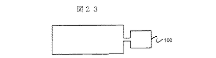
図22は、上記文献に開示されているデバイス構造を示す平面配置図である。平面配置は従来の単結晶シリコン基板に形成されたMOSFETと同じ配置を採用している。この構造の特徴は、薄い単結晶シリコン層より成る活性領域100の一部がゲ−ト(電極)500と同一の形状でパタ−ニングされている。そして、ゲ−トのコンタクト600において、そのゲート500と同時に活性領域に対して配線によりコンタクトされている。
【0008】
図23は、図22の活性領域100のみを示したもので、ゲ−トのコンタクト部では、いわゆるドックボ−ンのかたちに活性領域がパタ−ニングされている。コンタクトの断面構造を図24に示す。図24に示した断面構造は、A−A切断断面図である。図24に示したように、ゲート500と活性領域100とのコンタクトは、ゲ−ト500及びゲート酸化膜910を突き抜いたコンタクトホ−ルを形成し、上記ゲート酸化膜910下の活性領域100を露出させ、上記コンタクトホール内に形成した金属配線700によって達成される。
【0009】
【発明が解決しようとする課題】
上記文献に開示された技術では、活性領域を加工する際に予めゲ−トに合わせた微細なパタ−ニングをする必要がある。コンタクト形成時には、ゲ−トを突き抜ける加工を行い、かつ、薄膜シリコン層を突き抜けないように加工を止める必要がある。そして、ゲ−トへのコンタクトをゲ−ト層側面(コンタクトホール内壁)で行わなければならない。このため、通常のMOSトランジスタプロセス(従来の単結晶基板にMOSトランジスタを形成するためのプロセス)と整合性のとれない加工上の問題があり、集積化には適さない。
【0010】
したがって、特殊な加工を施すことなく、基板フロ−ティングの問題を解決する必要がある。
【0011】
本発明の目的は、チャネル形成領域に電位を与える新規なSOI構造の半導体装置を提供することにある。
【0012】
本発明の他の目的は、チャネル形成領域に電位を与える新規なSOI構造の絶縁ゲード電界効果トランジスタが一つの支持基体に複数構成された半導体集積回路装置を提供することにある。
【0013】
さらに、本発明の他の目的は、チャネル形成領域に電位を与えるための新規なSOI構造の半導体装置の製造方法を提供することにある。
【0014】
【課題を解決するための手段】
本発明の半導体装置によれば、絶縁体上に半導体単結晶層(polycrystalline semiconductor layer)が設けられ、該半導体単結晶層に形成されたゲ−ト、ソ−ス、ドレイン電極を有する絶縁ゲ−ト型電界効果トランジスタを含む半導体装置において、ゲート電極が上部ゲート層及び下部ゲート層の2層構造からなり、その上部ゲート層が該絶縁ゲ−ト型電界効果トランジスタのチャネル形成領域と電気的に接続されていることを特徴とする。
【0015】
本発明によれば、ゲート電極を介して基板バイアスされるため、基板フロ−ティングの問題は回避できる。
【0016】
また、後述する形成工程の説明で明らかなように本発明構造は自己整合的に実現されるため、従来技術のような加工上、整合性が取れないなどの問題を生じることがないのは明らかである。
【0017】
すなわち、下部ゲート電極の加工時に、SOI層(半導体単結晶層)まで連続してエッチングにより加工し、SOI層の側面を露出させる。この加工によりゲートとSOI層(すなわち、チャネル形成領域)とのコンタクトのための側面部が形成される。そして、下部ゲート層上に上部ゲート層を堆積することで自動的に下部ゲート層とSOI層とがその側面部において接続される。
【0018】
【発明の実施の形態】
以下、本発明の詳しい内容を実施例に基づき説明する。
【0019】
図1は、本発明における第1の実施例であって、SOI構造の半導体装置をマスクレイアウトで示した代表的な平面図である。まず、Nチャンネル型絶縁ゲート電界効果トランジスタ(以下、簡単に‘NMOS’として示す)に例をとり、その構造及び形成工程を説明する。
【0020】
太線で示した矩形の活性領域(薄い単結晶シリコン層)100を跨ようにゲ−トパターン500が位置されている。300Aは、N型不純物をイオン打ち込みしてNMOSのソ−ス、ドレイン電極を形成するときの開口マスクの位置を示す。600は、ソース領域、ドレイン領域及びゲート電極それぞれに対する配線のコンタクト部を示す。また、700は配線の位置を示している。
【0021】
上記配置のNMOSの断面構造を図2、図3、図4に示す。図2、図3および図4は、それぞれ、図1におけるA−A線(チャネル垂直方向またはチャネル幅方向)、B−B線(チャネル長方向)およびC−C線での切断断面である。それぞれの図において、120は例えば高抵抗単結晶シリコンより成る支持基板(body)である。110は絶縁膜であり、例えばシリコン酸化膜より成る。100は絶縁膜110上に位置された第1導電型単結晶シリコン層(すなわち、SOI層)である。910はゲート絶縁膜であり、具体的にはシリコン酸化膜より成る。550は下部ゲート層、500は上部ゲート層である。350は第1導電型に対して反対の導電型を示すソース、ドレイン拡散層(source/dorain diffused layers)である。チャネル部のシリコン、すなわちSOI層100は、低濃度のP導電型を示す。ソース、ドレイン拡散層はN導電型を示す。700は金属配線層を示し、それぞれの拡散層および電極にコンタクトされている。
【0022】
本発明の特徴を図2に示す。図2において、SOI層100における互いに対向する両側面は、ゲート絶縁膜910がないため、上部ゲート層500と接しており電気的導通がとられている。よって、金属配線700に印加されたバイアスは、上層ゲート層500を介してSOI層100(ゲート電極下のチャンネル形成領域)に与えられる。また、下部ゲート層550はゲート絶縁膜910を介して電界効果を及ぼし、電界効果トランジスタ(FET)としての動作を行うことができる。そして、図4に示すように、SOI層100の側面と拡散層350とが離れて配置されている。すなわち、拡散層350とSOI層100とで構成されるPN接合はSOI層100の側面に到達しないようにそのSOI層100内に形成される。ゲートとのコンタクト部と拡散層の間に距離があるため、ゲートとドレイン間の耐圧は充分得ることができる。
【0023】
図3に示す断面構造に対応させて、他の実施例をそれぞれ図5、図6および図7に示す。
【0024】
図5に示した第2の実施例は、SOI層100を薄膜化した場合を示している。このSOI層100の厚さは、例えば10nmを有し、ゲート絶縁膜910の厚さはそのSOI層100の厚さの約1/2である。
【0025】
本実施例におけるゲートとチャンネル形成領域との電気的な接続は、図2に示した構造により達成される。
【0026】
本実施例によれば、サブスレショールド動作領域(subthreshold operation region)での特性改善が図れる。すなわち、ゲート電極とチャンネル活性領域とが電気的に接続されているため、トランジスタ(NMOS)のゲート電圧(VG)=0Vの時(オフ状態)には、そのトランジスタのオフ状態を強くする。つまり、スレショールド電圧を上げる。したがって、サブスレショールドリーク電流(subthreshold leakage current) の低減を図ることが出来る。
【0027】
また、SOI構造の固有の効果であるが、拡散層の寄生容量を低減することができる。
【0028】
図6に示した第3の実施例は、LDD(Lightly Doped Drain)構造として知られる浅い低濃度不純物拡散層340を設けたSOI構造のNMOSである。すなわち、この拡散層金属配線が接続されるソース、ドレイン拡散層よりも低濃度を有し、かつ浅く形成されている。このようにLDD構造を採用したことにより、ホットエレクトロン効果(hot electron effect)を低減することができ、 SOI構造のNMOSの微細化が図れる。
【0029】
そして、本実施例におけるゲートとチャンネル形成領域との電気的な接続は、図2に示した構造により達成される。
【0030】
なお、図6において、ゲート電極500、550に対するサイドウオールスペーサ(sidewall spacer)は省略されている。
【0031】
図7に示した第4の実施例は、DDD(Double Diffused Drain)構造と呼ばれる低濃度拡散層340で、金属配線700が接続される高濃度拡散層350を包んだ構造であり、ドレイン耐圧を向上することができる。
【0032】
本実施例においても、ゲートとチャンネル形成領域との電気的な接続は、図2に示した構造により達成される。
【0033】
なお、図7において、高濃度拡散層350は、ゲート電極500、550の端部(edge)から離れている。しかし、実際は低濃度拡散層340と同様にゲート電極500、550の端部(edge)に対して自己整合(self align)形成される。このため、ゲート絶縁膜109に接した高濃度拡散層350の端部はゲート電極下に位置する。
【0034】
次に、図1に示した第1の実施例の製造方法を説明する。
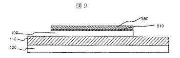
図8から図11は、第1の実施例の製造過程を示す断面構造図である。図8から図11は、図1に示したゲ−トを含んだ半導体装置のA−A線切断断面での製造過程である。
【0035】
図8に示すように、支持基板としてのシリコン基板120上にシリコン酸化膜110が形成される。シリコン基板120は比較的高抵抗の単結晶シリコン(relatively high resistivity single crystalline silicon)である。そして、そのシリコン酸化膜110上に厚さ100nm、P導電型(P−conductivity type)の1Ω cmの抵抗率(resistivity)を有する単結晶シリコン層(SOI層)100が形成される。これにより、スターテングマテリアル(starting material)としてのSOI基板が準備される。そして、このSOI基板表面に、熱酸化により10nmのゲート酸化膜910を形成し、そして、CVD法を用いてP導電型にドーピングされた多結晶シリコン層550を100nm堆積する。
【0036】
次に、図9に示すように、ホトレジスト法を用いて活性領域をパタ−ニングする。すなわち、ホトレジマスクを用いて下部ゲート層550、ゲート絶縁膜910、SOI層100を順次エッチング加工する。このとき、SOI層100側面を活性領域の形に露出させることができる。
【0037】
なお、活性領域(active region)は絶縁ゲート電界効果トランジスタが形成される領域を言い、ソース、ドレイン領域(source and drain regions)及びそれらの間のチャンネル形成領域を含んでいる。
【0038】
次に、図10に示すように、CVD法を用いて、高濃度にボロンをド−ピングした多結晶シリコン(上部ゲート層)500を堆積する。これにより、下部ゲート層550とSOI層100とが露出したSOI層側面で接続される。多結晶シリコン中にドーピングされたボロンは、以降の熱処理工程(例えばCVD保護膜形成等の熱処理)によりSOI層側面から拡散し、SOI層中に高濃度層を形成する。この高濃度層は、プロセスを低温化(例えば、60000℃〜700℃程度)することで薄くすることができるため、図中では、省略する。
【0039】
次に、図11に示すように、ホトレジスト法により、ゲ−ト電極をパターニングする。具体的には、異方性ドライエッチングによりゲ−ト電極加工を行う。このとき、SOI層110上では、上部ゲート層500と下部ゲート層550とを一緒に加工することができる。すなわち、図1に示したように、ゲート電極(500)は形成される。
【0040】
一般的に、SOI層100のような段差があると、そのSOI層側面に上部ゲート層550のエッチング残り(etching residue)が生じる。しかしながら、ゲート絶縁膜910と上部ゲート層550とのエッチングの選択比の高い条件を用いることで、加工することができる。
【0041】
以下、通常のMOSFETと同様な形成工程のため図は省略する。ゲ−ト電極500および開口マスク300A(図1参照)をマスクにヒ素(Arsenic)をイオンドーズ量5×1015cm2、打ち込みエネルギー25keVで加速したイオン打ち込み(ion−implantation)し、その後アニールすることで、拡散層(ソース、ドレイン領域)300を形成する。開口マスク300Aを用いることで、拡散層と、ゲート電極とコンタクトしているSOI層側面との間を0.3ミクロン(um)離した。これにより、ゲート500からSOI層表面に拡散して形成されているP型高濃度層(浅い接合のため図示せず)と、拡散層300との接合耐圧を上げることができる。そして、CVD法により、BPSG(Boro−Phosho Silicate Glass)を堆積し、熱処理することで平坦化してからそれぞれの電極にコンタクトを形成する。金属配線を堆積加工することで、素子(NMOS)が形成される。
【0042】
上記の工程から明らかなように、 SOI層にはコンタクトパターンを設けることなく、基板100とゲート電極を導通させることができる。
【0043】
なお、ここで用いた導電型を反対にすることで、PMOS(PチャネルMOS)が形成できる。また、 シリコン酸化膜110上にP導電型SOI層とN導電型SOI層をそれぞれ設け、PMOS形成用マスクとNMOS形成用マスクとを使い分けることでCMOSプロセスが達成できることは明らかである。
【0044】
図12は、第5の実施例を示す。特に、大きな電流をとるため、複数ゲート(電極)を平行に配置した、いわゆるデュアルゲート(dual gate)構造を有するSOI−NMOSのレイアウトを示している。図12において、拡散層300は、活性領域(SOI層)100のパターンよりも小さく形成されている。
【0045】
本実施例においても、それぞれのゲート電極500は、図2に示すように、上部ゲート層及び下部ゲート層より成る2層構造を有し、上部ゲート層と活性領域の側面にコンタクトしている。
【0046】
本発明構造および形成プロセスを用いると、拡散層とは反対導電型を持つ電極(P導電型ゲート電極500)と活性領域とのコンタクトはそれらが同一導電型であるため容易に達成できる。また、バイポーラトランジスタが同時に得られる。
【0047】
図13は、第6の実施例であり、そのバイポーラトランジスタの基本的な配置を示す。例えばPMOSの場合、そのトランジスタの構成は、ゲート500が接続されたN導電型SOI層をN型ベースとし、P型ソース領域およびP型ドレイン領域をそれぞれ、エミッタおよびコレクタとし、横型PNPバイポーラトランジスタ(LateralPNP Bipolar Transistor) として動作させることができる。
【0048】
図14は本発明の第7の実施例の半導体装置の平面配置図である。本実施例はMOSFETではなく、横型バイポーラトランジスタのみを構成している。すなわち、図14に示すように、電極500はベース引き出し電極としてパターンニングされている。前記第6の実施例と同様に、この電極500はSOI層100側面に接続されている。エミッタ領域及びコレクタ領域は開口マスクパターン300、310をマスクとして周知のイオン打ち込みによりSOI層100内に選択的に形成することができる。
【0049】
図15は、本発明の第8の実施例の半導体装置の平面配置図である。
図15に示すように、リング状に活性領域(SOI層)100を絶縁膜(図示せず)に配置させ、デバイスを形成することができる。このデバイスは、たとえばSOI−MOSFETの入力保護用ダイオード(PN接合ダイオード)として適用できる。すなわち、N導電型SOI層100にP導電型拡散層300が上記絶縁膜に達するように選択的に形成されている。 P導電型高濃度不純物拡散層300が形成されているリング状SOI層100の内側の側壁には電極500がコンタクトされている。電極500主面およびSOI層主面に層間絶縁膜(図示せず)が被覆され、この層間絶縁膜にはコンタクトホール600が配置されている。そして、点線で示したように、アノード配線MAおよび配線MKが接続されている。
【0050】
本実施例によれば、電極500がPN接合(PN junction)全体に対向してリング状SOI層100の内側の側壁にコンタクトされているため、サージ電流を均一に流すことが可能である。
【0051】
次に、図16から図18に第9の実施例である他の半導体装置の製造方法を示す。
【0052】
なお、図16から図18に示した断面図は図1に示すA−A線切断方向の断面図に対応する。
【0053】
図9に示した下部ゲート層550を加工する時に、下部ゲート層550上にシリコン窒化膜925を堆積し、シリコン窒化膜925および下部ゲート層550のエッチングし、ゲ−ト絶縁膜910で加工を一旦止める。次に、既知のCVD法とドライエッチング(異方性エッチング:anisotropic etching)を組み合わせたスペーサ形成技術により、下部ゲート層550側面にスペーサ920を形成することができる(図16)。
【0054】
次に、シリコン窒化膜925およびスペーサ920をマスクにSOI層100を加工する(図17)。
【0055】
次に、スペーサ920およびにシリコン窒化膜925を除去し、下部ゲート層550をマスクにイオン打ち込みすることで、SOI層100周辺部に自己整合的にP導電型の高濃度不純物拡散層330を設けることができる。この後、図10に示した実施例1の形成プロセス (ゲートエッチング)を行うことで素子を得ることができる(図18)。このプロセスを行うことで、金属材を上部ゲート層500として用いても、 SOI層(基板)とショットキーバリア(schottky barrier)を持つことなく低抵抗で導通を得ることができる。
【0056】
本発明構造では、異なる材質を積層することでゲートを形成できることは明らかであり、必要なゲート抵抗を得るように組み合わせを設計することができる。これまで、2層のゲート構成を示してきたが、例えば、下部ゲートをN型多結晶シリコンとそのN型多結晶シリコン上のチタンナイトライド(TiN)との積層膜とし、上部ゲートをP型多結晶シリコンにすることができる。すなわち、ゲートの低抵抗化や閥値(threshold voltage)設定のため開発されているポリサイドゲート(polyside gate)やサリサイドゲート(salicide gate)のような積層ゲート構造をそのまま用いることができる。
【0057】
図19は、第10の実施例であり、上部ゲート500と、下部ゲート550との間に絶縁膜930を置いた場合を示している。これにより、容易に浮遊ゲート型メモリセルを得ることができる。
【0058】
したがって、 SOI層100に前記実施例(例えば第1の実施例)のような上部ゲート層及び下部ゲート層より成る2層構造を有し、上部ゲート層と活性領域の側面にコンタクトしているMOSFETと上記浮遊ゲート型メモリセルとが搭載された半導体集積回路装置を形成することが可能である。
【0059】
また、図20および図21は、それぞれ第11の実施例および第12の実施例であり、前記実施例のMOSFETとともにSOI層100に形成が可能なPN接合ダイオードの変形例を示す。
【0060】
図20に示したダイオードは、 P導電型SOI層(基板)100とN型層370との間のPN接合で構成される。このダイオードの形成方法を以下に簡単に述べる。
【0061】
まず、ゲート絶縁膜を基板100表面に置かずに下部ゲート層550および上部ゲート層500を堆積する。具体的には、図8に示したゲート絶縁膜910を形成した後、ダイオドが形成されるべき基板100表面に形成されたゲート絶縁膜910の一部を除去する。そして、下部ゲート層550および上部ゲート層500を堆積する。ゲート電極パターンニング工程で、そのゲート絶縁膜がないため、基板100をエッチングすることができる。この時作られる側面の段差を利用して絶縁膜スペーサ960を形成する。そして、露出した多結晶シリコン500および、基板100に選択的にタングステン710を堆積する。基板100にはタングステン堆積前にリンをイオン打ち込みすることにより、上記絶縁膜スペーサ960によって規定されたN型層370を形成する。360はゲート絶縁膜がないため550より拡散してくるP型不純物層を示したものである。
【0062】
本実施例は、2層ゲートパターンエッチングを利用して、PN接合ダイオードを選択的に形成できる。
【0063】
CM0Sプロセスでは、ゲートの多結晶シリコンにN型およびP型の両者を用いられている。これを利用することで、ダイオードを形成することができる。図21に代表的レイアウトを示す。活性領域(P導電型SOI層)100の左側面(CNT1)よりN導電型領域へのコンタクトが行われ、右側面(CNT2)よりP導電型領域へのコンタクトをとることができる。
【0064】
なお、 N導電型領域300は開口マスク300Aを用いたヒ素イオンの打ち込みにより形成される。
【0065】
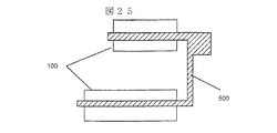
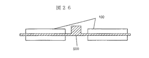
本発明によるゲートと基板(SOI層)とのコンタクト(以下、基板コンタクトと言う)は、ゲートが複数の活性領域に跨るときに有効である。つまり、本発明は高集積化に適した構造である。図25、図26そして図27は、第13、第14そして第15の実施例をそれぞれ示す。LSIで使用されている代表的な活性領域100とゲート500との配置例をそれぞれ示す。
【0066】
従来の基板コンタクトでは、複数のコンタクト形成領域を設ける必要がある。
【0067】
しかしながら、本発明によれば、活性領域100の側壁で基板コンタクトを達成しているため、図25から図27それぞれ示した配置の活性領域に対する基板コンタクトが容易に行える。したがって、高集積化された低電圧駆動の半導体集積回路装置が得られる。
【0068】
ところで、本発明のデバイス構造は、高い電圧(Vcc=1.2V〜1.5V)では、リーク電流が増大するため、特に低い電圧(VDL≦0.6V)での動作において効果がある。このため、基板コンタクトの無いSOI−MOSFETと本発明のような基板コンタクトを有するSOI−MOSFETとを集積化した半導体集積回路装置(以下、ICと言う)の場合、図28に示したような電圧リミッタ(voltage limitor)をそのIC内に設け、駆動電圧VDLによって動作させる内部回路(internal circuit)を上記本発明のSOI−MOSFETsで構成することができる。
【0069】
なお、図28において、抵抗R1、R2は基準電圧Vref(≦0.6V)が得られるように設定される。DAは差動アンプ(differntial amplifier)である。
【0070】
本発明のSOI−MOSFETsをゲート保護回路素子として用いた実施例を図29に示す。本実施例では、IC内において、ボンデイングパッド(bonding pad)BPと内部回路1との間に本発明で構成された大きなインバータ(CMOSインバータ)を接続することで、ゲート保護素子として動作させることが出来る。すなわち、ゲート電極は電源Vccあるいは接地線Vssに対し、それぞれPN接合を介して接続されている。このため、たとえば、正のサージ電圧がボンデイングパッドBPに印加された場合、NMOSのPN接合を通して、接地線Vssに引き抜かれる。一方、負のサージ電圧がボンデイングパッドBPに印加された場合、PMOSのPN接合を通して、接地線Vccに引き抜かれる。
【0071】
本発明によれば、低電圧で動作する特性を有する。したがって、電圧の低さが課題であった光起電力効果(phtovoltaic effect)を利用した受光素子(photodetector)、例えば太陽電池(solar cell)と本発明のSOI−MOSFETsとを集積化することができる。たとえば、図30に示した電子カードが組み立てられる。図30において、シリコン基板120に設けられたウエル(well)に受光素子122が形成され、その基板120の一部に埋め込み酸化膜110が形成されている。埋め込み酸化膜110上には本発明のSOI−MOSFETsが形成されている。そして、たとえば、透明な樹脂体10でシリコン基板120が封止されている。そしてさらに、樹脂体10のコーナには外部端子11が設けられている。
【0072】
なお、本発明のSOI−MOSFETsを基板120の一方の主面に設け、その一方の主面と反対の他方の主面に受光素子を設け、一方の主面は不透明の樹脂体で保護し、そして、他方の主面は透明な樹脂体で保護してもよい。
【0073】
【発明の効果】
本発明によれば、ゲート電極が、チャネルとなる基板と電気的に接続されるため、チヤネルに対して給電できるため、基板フローテイングの問題を抑えることができる。
【0074】
また、ゲート電極とチャネルとなる基板との電気的な接続は基板側面部おいて達成するため、基板コンタクトエリアの占有面積が無く高集積化が可能となる。
【図面の簡単な説明】
【図1】本発明の第1の実施例である半導体装置を示す平面図である。
【図2】図1に示した半導体装置のA−A線切断断面である。
【図3】図1に示した半導体装置のB−B線切断断面である。
【図4】図1に示した半導体装置のC−C線切断断面である。
【図5】本発明の第2の実施例の半導体装置を示す断面図である。
【図6】本発明の第3の実施例の半導体装置を示す断面図である。
【図7】本発明の第4の実施例の半導体装置を示す断面図である。
【図8】図1に示した半導体装置の製造過程を示す断面図である。
【図9】図8に続く半導体装置の製造過程を示す断面図である。
【図10】図9に続く半導体装置の製造過程を示す断面図である。
【図11】図10に続く半導体装置の製造過程を示す断面図である。
【図12】本発明の第5の実施例の半導体装置の平面配置図である。
【図13】本発明の第6の実施例の半導体装置の平面配置図である。
【図14】本発明の第7の実施例の半導体装置の平面配置図である。
【図15】本発明の第8の実施例の半導体装置の平面配置図である。
【図16】本発明の第9の実施例の半導体装置の製造過程を示す断面図である。
【図17】本発明の第9の実施例の半導体装置の製造過程を示す断面図である。
【図18】本発明の第9の実施例の半導体装置の製造過程を示す断面図である。
【図19】本発明の第10の実施例の半導体装置を示す断面図である。
【図20】本発明の第11の実施例の半導体装置を示す断面図である。
【図21】本発明の第12の実施例の半導体装置の平面配置図である。
【図22】従来のSOI構造の半導体装置の平面図である。
【図23】図22に示した従来の半導体装置の薄膜単結晶シリコン層の平面図である。
【図24】図22に示した従来の半導体装置のA−A線切断断面である。
【図25】本発明の第13の実施例半導体集積回路装置の平面図である。
【図26】本発明の第14の実施例である半導体集積回路装置の平面図である。
【図27】本発明の第15の実施例である半導体集積回路装置の平面図である。
【図28】本発明のそれぞれの実施例の半導体装置(または半導体集積回路装置)を駆動するための電源回路(電圧リミッタ)を示す回路図である。
【図29】本発明の半導体装置を保護素子として用いた入出力保護回路を示す回路図である。そして、
【図30】本発明の半導体装置(または半導体集積回路装置)が組み込まれた電子カードを示す断面図である。
【符号の説明】
100:SOI活性領域。
110:シリコン酸化膜層。
120:支持基板。
300A:開ロマスク
300,330、340、350、360、370:高濃度不純物拡散層。
500、550:ゲート。
600:コンタクト。
700、710:金属配線。
910:ゲート酸化膜。1
920、930、960:層間絶縁膜
10:電子カード。[0001]
TECHNICAL FIELD OF THE INVENTION
The present invention relates to a semiconductor device, and more particularly to an insulated gate field effect transistor having an SOI (Silicon On Insulator) structure.
[0002]
[Prior art]
An SOI-MOSFET (Silicon On Insulator-Metal Oxide Semiconductor Field Effect Transistor) formed in a thin single crystal silicon layer over an insulating substrate can be largely integrated on one substrate by using a microfabrication process of silicon. Also, attention has been paid to the fact that the formed transistor has a smaller parasitic capacitance and is suitable for high-speed operation as compared with the case where a conventional single crystal silicon substrate is used.
[0003]
In a conventional semiconductor device (MOSFET) using a single crystal silicon substrate, a channel is biased using a substrate electrode. On the other hand, in the SOI-MOSFET, since the insulating layer (or insulating substrate) is provided at the bottom of the thin single-crystal silicon layer, the bias cannot be applied from below the channel, causing unstable operation. (Floating-substrate).
[0004]
That is, in an NMOS (N-channel MOS), a large leak current flows in the off state by accumulating holes in the channel portion, and a kink effect occurs in the current characteristics even in the on state. Is reported to occur. It is known that this problem appears remarkably in an NMOS having a large impact ionization coefficient.
[0005]
A technique for solving this problem is disclosed in, for example, JP-A-4-34980 or JP-A-7-273340.
[0006]
Also, Eye, A-, A-, A-, Electron Device Letters, December 1994, pp. 510 to 512 (IEEE Electron Devices Letters, vol. 15, No. 12, pp. 510-512). As described in December 1994), it has been considered to bias the channel portion (P-silicon) via a gate electrode. The MOSFET having the structure connecting the substrate and the gate can be regarded as a device in which the FET and a lateral bipolar device coexist. According to such a MOSFET, it is reported that excellent characteristics can be obtained particularly in low-voltage operation (0.6 V or less).
[0007]
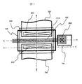
FIG. 22 is a plan view showing a device structure disclosed in the above document. The planar arrangement employs the same arrangement as a MOSFET formed on a conventional single crystal silicon substrate. The feature of this structure is that a part of the
[0008]
FIG. 23 shows only the
[0009]
[Problems to be solved by the invention]
In the technique disclosed in the above-mentioned document, it is necessary to perform fine patterning in advance according to the gate when processing the active region. At the time of contact formation, it is necessary to perform processing to penetrate the gate and stop the processing so as not to penetrate the thin film silicon layer. The contact to the gate must be made on the side surface of the gate layer (the inner wall of the contact hole). For this reason, there is a problem in processing that is not compatible with a normal MOS transistor process (a process for forming a MOS transistor on a conventional single crystal substrate), which is not suitable for integration.
[0010]
Therefore, it is necessary to solve the problem of substrate floating without performing special processing.
[0011]
It is an object of the present invention to provide a novel SOI structure semiconductor device for applying a potential to a channel formation region.
[0012]
Another object of the present invention is to provide a semiconductor integrated circuit device in which a plurality of novel insulated gate field effect transistors having a novel SOI structure for applying a potential to a channel formation region are formed on one supporting base.
[0013]
Still another object of the present invention is to provide a method for manufacturing a semiconductor device having a novel SOI structure for applying a potential to a channel formation region.
[0014]
[Means for Solving the Problems]
According to the semiconductor device of the present invention, a semiconductor single crystal layer (polycrystalline semiconductor layer) is provided on an insulator, and an insulating gate having a gate, a source, and a drain electrode formed on the semiconductor single crystal layer is provided. In a semiconductor device including a gate type field effect transistor, a gate electrode has a two-layer structure of an upper gate layer and a lower gate layer, and the upper gate layer is electrically connected to a channel forming region of the insulated gate field effect transistor. It is characterized by being connected.
[0015]
According to the present invention, since the substrate is biased through the gate electrode, the problem of substrate floating can be avoided.
[0016]
Further, as will be apparent from the description of the forming process described later, since the structure of the present invention is realized in a self-alignment manner, it is apparent that there is no problem such as inconsistency in processing as in the prior art. It is.
[0017]
That is, when the lower gate electrode is processed, the SOI layer (semiconductor single crystal layer) is continuously processed by etching to expose the side surface of the SOI layer. By this processing, a side surface portion for contact between the gate and the SOI layer (that is, a channel formation region) is formed. Then, by depositing the upper gate layer on the lower gate layer, the lower gate layer and the SOI layer are automatically connected at the side surface.
[0018]
BEST MODE FOR CARRYING OUT THE INVENTION
Hereinafter, the details of the present invention will be described based on examples.
[0019]
FIG. 1 shows a first embodiment of the present invention and is a typical plan view showing a semiconductor device having an SOI structure in a mask layout. First, an example of an N-channel insulated gate field effect transistor (hereinafter simply referred to as “NMOS”) will be described in terms of its structure and formation process.
[0020]
A
[0021]
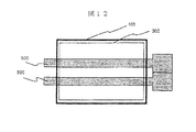
The cross-sectional structure of the NMOS having the above arrangement is shown in FIGS. 2, 3, and 4 are cross-sectional views taken along line AA (in a channel vertical direction or channel width direction), line BB (in a channel length direction), and line CC in FIG. 1, respectively. In each of the drawings,
[0022]
FIG. 2 shows the features of the present invention. In FIG. 2, both side surfaces of the
[0023]
Other embodiments are shown in FIGS. 5, 6, and 7, respectively, corresponding to the cross-sectional structure shown in FIG.
[0024]
The second embodiment shown in FIG. 5 shows a case where the
[0025]
The electrical connection between the gate and the channel formation region in this embodiment is achieved by the structure shown in FIG.
[0026]
According to the present embodiment, characteristics can be improved in a sub-threshold operation region. That is, since the gate electrode and the channel active region are electrically connected, when the gate voltage (VG) of the transistor (NMOS) is 0 V (off state), the off state of the transistor is strengthened. That is, the threshold voltage is increased. Therefore, it is possible to reduce the sub-threshold leakage current.
[0027]
Also, as an effect inherent to the SOI structure, the parasitic capacitance of the diffusion layer can be reduced.
[0028]
The third embodiment shown in FIG. 6 is an SOI-structure NMOS provided with a shallow low-concentration
[0029]
The electrical connection between the gate and the channel formation region in this embodiment is achieved by the structure shown in FIG.
[0030]
In FIG. 6, side wall spacers for the
[0031]
The fourth embodiment shown in FIG. 7 is a structure in which a low-
[0032]
Also in this embodiment, the electrical connection between the gate and the channel formation region is achieved by the structure shown in FIG.
[0033]
In FIG. 7, the high-
[0034]
Next, the manufacturing method of the first embodiment shown in FIG. 1 will be described.
8 to 11 are sectional structural views showing the manufacturing process of the first embodiment. 8 to 11 show a manufacturing process of the semiconductor device including the gate shown in FIG. 1 in a section cut along the line AA.
[0035]
As shown in FIG. 8, a
[0036]
Next, as shown in FIG. 9, the active region is patterned by using a photoresist method. That is, the
[0037]
The active region refers to a region where an insulated gate field effect transistor is formed, and includes a source and drain region and a channel forming region between the source and drain regions.
[0038]
Next, as shown in FIG. 10, polycrystalline silicon (upper gate layer) 500 doped with boron at a high concentration is deposited by using the CVD method. Thus, the
[0039]
Next, as shown in FIG. 11, the gate electrode is patterned by a photoresist method. Specifically, gate electrode processing is performed by anisotropic dry etching. At this time, the
[0040]
Generally, when there is a step like the
[0041]
Hereinafter, since the formation process is the same as that of a normal MOSFET, the drawing is omitted. Arsenic is ion-
[0042]
As is clear from the above steps, the
[0043]
The PMOS (P-channel MOS) can be formed by reversing the conductivity type used here. It is apparent that a CMOS process can be achieved by providing a P-conductivity-type SOI layer and an N-conductivity-type SOI layer on the
[0044]
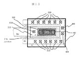
FIG. 12 shows a fifth embodiment. In particular, the layout of an SOI-NMOS having a so-called dual gate structure in which a plurality of gates (electrodes) are arranged in parallel to obtain a large current is shown. In FIG. 12, the
[0045]
Also in this embodiment, each
[0046]
Using the structure and formation process of the present invention, contact between the electrode having the opposite conductivity type to the diffusion layer (P-conductivity type gate electrode 500) and the active region can be easily achieved because they have the same conductivity type. Further, a bipolar transistor can be obtained at the same time.
[0047]
FIG. 13 shows a sixth embodiment, showing a basic arrangement of the bipolar transistor. For example, in the case of a PMOS, the configuration of the transistor is such that an N-conductivity-type SOI layer to which a
[0048]
FIG. 14 is a plan layout view of a semiconductor device according to a seventh embodiment of the present invention. In this embodiment, only a lateral bipolar transistor is formed, not a MOSFET. That is, as shown in FIG. 14, the
[0049]
FIG. 15 is a plan layout view of a semiconductor device according to an eighth embodiment of the present invention.
As shown in FIG. 15, a device can be formed by disposing the active region (SOI layer) 100 in a ring shape on an insulating film (not shown). This device can be applied, for example, as an input protection diode (PN junction diode) of an SOI-MOSFET. That is, the P conductivity
[0050]
According to the present embodiment, since the
[0051]
Next, FIGS. 16 to 18 show a method of manufacturing another semiconductor device according to the ninth embodiment.
[0052]
The cross-sectional views shown in FIGS. 16 to 18 correspond to the cross-sectional views taken along the line AA shown in FIG.
[0053]
When processing the
[0054]
Next, the
[0055]
Next, the
[0056]
In the structure of the present invention, it is clear that a gate can be formed by laminating different materials, and a combination can be designed so as to obtain a necessary gate resistance. So far, a two-layer gate structure has been described. For example, the lower gate is a laminated film of N-type polycrystalline silicon and titanium nitride (TiN) on the N-type polycrystalline silicon, and the upper gate is P-type. It can be polycrystalline silicon. That is, a stacked gate structure such as a polyside gate and a salicide gate, which are developed for lowering the gate resistance and setting a threshold voltage, can be used as it is.
[0057]
FIG. 19 shows the tenth embodiment, in which an insulating
[0058]
Therefore, the
[0059]
20 and 21 show an eleventh embodiment and a twelfth embodiment, respectively, showing modified examples of the PN junction diode that can be formed in the
[0060]
The diode shown in FIG. 20 includes a PN junction between P-type SOI layer (substrate) 100 and N-
[0061]
First, the
[0062]
In the present embodiment, a PN junction diode can be selectively formed using two-layer gate pattern etching.
[0063]
In the CM0S process, both N-type and P-type are used for the polysilicon of the gate. By utilizing this, a diode can be formed. FIG. 21 shows a typical layout. The left side surface (CNT1) of the active region (P conductive type SOI layer) 100 is in contact with the N conductive type region, and the right side surface (CNT2) is in contact with the P conductive type region.
[0064]
The N
[0065]
The contact between the gate and the substrate (SOI layer) according to the present invention (hereinafter referred to as the substrate contact) is effective when the gate extends over a plurality of active regions. That is, the present invention has a structure suitable for high integration. FIGS. 25, 26 and 27 show thirteenth, fourteenth and fifteenth embodiments, respectively. An example of the arrangement of a typical
[0066]
In a conventional substrate contact, it is necessary to provide a plurality of contact formation regions.
[0067]
However, according to the present invention, since the substrate contact is achieved on the side wall of the
[0068]
By the way, the device structure of the present invention has a high cc = 1.2 V to 1.5 V), the leakage current increases, so that a particularly low voltage (V DL <0.6 V). For this reason, in the case of a semiconductor integrated circuit device (hereinafter, referred to as an IC) in which an SOI-MOSFET without a substrate contact and an SOI-MOSFET with a substrate contact as in the present invention are integrated, a voltage as shown in FIG. A limiter (voltage limiter) is provided in the IC, and the driving voltage V DL An internal circuit (internal circuit) operated by the SOI-MOSFETs of the present invention can be constituted.
[0069]
In FIG. 28, the resistors R1 and R2 are set such that a reference voltage Vref (≦ 0.6 V) is obtained. DA is a differential amplifier.
[0070]
FIG. 29 shows an embodiment using the SOI-MOSFETs of the present invention as a gate protection circuit element. In the present embodiment, a large inverter (CMOS inverter) configured according to the present invention is connected between a bonding pad BP and an
[0071]
According to the present invention, it has the characteristic of operating at low voltage. Therefore, a light receiving element (photodetector) using a photovoltaic effect, for which low voltage is a problem, for example, a solar cell (solar cell) and the SOI-MOSFETs of the present invention can be integrated. . For example, the electronic card shown in FIG. 30 is assembled. 30, a
[0072]
Note that the SOI-MOSFETs of the present invention are provided on one main surface of the
[0073]
【The invention's effect】
According to the present invention, since the gate electrode is electrically connected to the substrate serving as a channel, power can be supplied to the channel, so that the problem of substrate floating can be suppressed.
[0074]
In addition, since electrical connection between the gate electrode and the substrate serving as a channel is achieved at the side surface of the substrate, the area occupied by the substrate contact area is eliminated and high integration is possible.
[Brief description of the drawings]
FIG. 1 is a plan view showing a semiconductor device according to a first embodiment of the present invention.
FIG. 2 is a sectional view taken along line AA of the semiconductor device shown in FIG. 1;
FIG. 3 is a sectional view taken along line BB of the semiconductor device shown in FIG. 1;
FIG. 4 is a sectional view taken along line CC of the semiconductor device shown in FIG. 1;
FIG. 5 is a sectional view showing a semiconductor device according to a second embodiment of the present invention.
FIG. 6 is a sectional view showing a semiconductor device according to a third embodiment of the present invention.
FIG. 7 is a sectional view showing a semiconductor device according to a fourth embodiment of the present invention.
FIG. 8 is a cross-sectional view showing a manufacturing process of the semiconductor device shown in FIG. 1;
FIG. 9 is a sectional view illustrating the manufacturing process of the semiconductor device, following FIG. 8;
FIG. 10 is a sectional view illustrating the manufacturing process of the semiconductor device, following FIG. 9;
FIG. 11 is a sectional view illustrating the manufacturing process of the semiconductor device, following FIG. 10;
FIG. 12 is a plan layout view of a semiconductor device according to a fifth embodiment of the present invention.
FIG. 13 is a plan layout view of a semiconductor device according to a sixth embodiment of the present invention.
FIG. 14 is a plan layout view of a semiconductor device according to a seventh embodiment of the present invention.
FIG. 15 is a plan layout view of a semiconductor device according to an eighth embodiment of the present invention.
FIG. 16 is a sectional view showing a manufacturing process of the semiconductor device according to the ninth embodiment of the present invention;
FIG. 17 is a sectional view illustrating a manufacturing process of the semiconductor device according to the ninth embodiment of the present invention;
FIG. 18 is a sectional view showing a manufacturing process of the semiconductor device according to the ninth embodiment of the present invention.
FIG. 19 is a sectional view showing a semiconductor device according to a tenth embodiment of the present invention.
FIG. 20 is a sectional view showing a semiconductor device according to an eleventh embodiment of the present invention.
FIG. 21 is a plan layout view of a semiconductor device according to a twelfth embodiment of the present invention.
FIG. 22 is a plan view of a conventional semiconductor device having an SOI structure.
FIG. 23 is a plan view of a thin-film single-crystal silicon layer of the conventional semiconductor device shown in FIG.
FIG. 24 is a sectional view taken along line AA of the conventional semiconductor device shown in FIG. 22;
FIG. 25 is a plan view of a semiconductor integrated circuit device according to a thirteenth embodiment of the present invention.
FIG. 26 is a plan view of a semiconductor integrated circuit device according to a fourteenth embodiment of the present invention.
FIG. 27 is a plan view of a semiconductor integrated circuit device according to a fifteenth embodiment of the present invention.
FIG. 28 is a circuit diagram showing a power supply circuit (voltage limiter) for driving the semiconductor device (or semiconductor integrated circuit device) of each embodiment of the present invention.
FIG. 29 is a circuit diagram showing an input / output protection circuit using the semiconductor device of the present invention as a protection element. And
FIG. 30 is a cross-sectional view showing an electronic card in which the semiconductor device (or semiconductor integrated circuit device) of the present invention is incorporated.
[Explanation of symbols]
100: SOI active area.
110: silicon oxide film layer.
120: Support substrate.
300A: Open mask
300, 330, 340, 350, 360, 370: high concentration impurity diffusion layers.
500, 550: gate.
600: contact.
700, 710: metal wiring.
910: Gate oxide film. 1
920, 930, 960: interlayer insulating film
10: Electronic card.
Claims (9)
前記単結晶半導体層にゲート絶縁膜を介して第1導体層を堆積する工程と、
前記第1導体層および前記単結晶半導体層に対しゲート幅方向を規定するパターンニングを行う工程と、
パターンニングされた前記第1導体層および前記単結晶半導体層上に前記第1導体層主面及び側面、前記単結晶導体層の側面に接する第2導体層を堆積する工程と、
前記第2導体層及び前記第1導体層に対しゲート長方向を規定するパターンニングを行い、前記第1導体層で形成された第1ゲート層と、前記第2導体層で形成された、前記第1ゲート層の側面と接する前記第2ゲート層との積層ゲート電極を形成する工程とを有することを特徴とする半導体装置の製造方法。In a method of manufacturing a semiconductor device having an insulated gate field effect transistor in a single crystal semiconductor layer on an insulator,
Depositing a first conductive layer via a gate insulating film on the single crystal semiconductor layer,
And performing patterning for defining the gate width direction with respect to the first conductive layer and the single crystal semiconductor layer,
The patterned first conductive layer main surface and side surfaces on the first conductive layer and the single crystal semiconductor layer, depositing a second conductive layer in contact with the side surfaces of the single crystal conductive layer,
The second conductor layer and the first conductor layer are subjected to patterning defining a gate length direction, and the first gate layer formed of the first conductor layer and the second gate layer formed of the second conductor layer are formed. the method of manufacturing a semiconductor device characterized by a step of forming a stacked gate electrode and said second gate layer which is in contact with the side surface of the first gate layer.
前記単結晶半導体層上に絶縁膜を介して第1導体層を形成する工程と、Forming a first conductor layer on the single crystal semiconductor layer via an insulating film;
前記第1導体層を加工する工程と、Processing the first conductor layer;
前記単結晶半導体層を加工する工程と、Processing the single crystal semiconductor layer;
前記第1導体層の上面および側面と前記単結晶半導体層の側面に第2の導体層を堆積する工程と、Depositing a second conductor layer on top and side surfaces of the first conductor layer and side surfaces of the single crystal semiconductor layer;
前記第2導体層および前記第1導電層とを加工し、前記第2導電層が前記第1導体層の上面および側面と前記単結晶半導体層の側面に接続された、前記第1導体層および前記第2導体層を有するゲート電極を形成する工程とを有することを特徴とする半導体装置の製造方法。Processing the second conductive layer and the first conductive layer, wherein the second conductive layer is connected to an upper surface and a side surface of the first conductive layer and a side surface of the single crystal semiconductor layer; Forming a gate electrode having the second conductor layer.
Priority Applications (8)
| Application Number | Priority Date | Filing Date | Title |
|---|---|---|---|
| JP33963797A JP3545583B2 (en) | 1996-12-26 | 1997-12-10 | Semiconductor device and manufacturing method thereof |
| SG1997004585A SG74035A1 (en) | 1996-12-26 | 1997-12-19 | Semiconductor device and manufacturing method thereof |
| KR1019970072217A KR100712461B1 (en) | 1996-12-26 | 1997-12-23 | Semiconductor device and its manufacturing method |
| MYPI97006252A MY130168A (en) | 1996-12-26 | 1997-12-23 | Semiconductor device and manufacturing method thereof |
| TW086119685A TW437004B (en) | 1996-12-26 | 1997-12-24 | Semiconductor device and manufacturing method thereof |
| CN97126000A CN1131567C (en) | 1996-12-26 | 1997-12-26 | Semiconductor device and manufacturing method thereof |
| US08/998,887 US6060750A (en) | 1996-12-26 | 1997-12-29 | Semiconductor device having SOI-MOSFET |
| US09/506,956 US6194763B1 (en) | 1996-12-26 | 2000-02-18 | Semiconductor device having SOI-MOSFET |
Applications Claiming Priority (3)
| Application Number | Priority Date | Filing Date | Title |
|---|---|---|---|
| JP34713896 | 1996-12-26 | ||
| JP8-347138 | 1996-12-26 | ||
| JP33963797A JP3545583B2 (en) | 1996-12-26 | 1997-12-10 | Semiconductor device and manufacturing method thereof |
Publications (2)
| Publication Number | Publication Date |
|---|---|
| JPH10242477A JPH10242477A (en) | 1998-09-11 |
| JP3545583B2 true JP3545583B2 (en) | 2004-07-21 |
Family
ID=26576478
Family Applications (1)
| Application Number | Title | Priority Date | Filing Date |
|---|---|---|---|
| JP33963797A Expired - Fee Related JP3545583B2 (en) | 1996-12-26 | 1997-12-10 | Semiconductor device and manufacturing method thereof |
Country Status (7)
| Country | Link |
|---|---|
| US (2) | US6060750A (en) |
| JP (1) | JP3545583B2 (en) |
| KR (1) | KR100712461B1 (en) |
| CN (1) | CN1131567C (en) |
| MY (1) | MY130168A (en) |
| SG (1) | SG74035A1 (en) |
| TW (1) | TW437004B (en) |
Families Citing this family (61)
| Publication number | Priority date | Publication date | Assignee | Title |
|---|---|---|---|---|
| JP3545583B2 (en) * | 1996-12-26 | 2004-07-21 | 株式会社ルネサステクノロジ | Semiconductor device and manufacturing method thereof |
| JP3388195B2 (en) * | 1998-12-22 | 2003-03-17 | シャープ株式会社 | Semiconductor device and manufacturing method thereof |
| KR100361861B1 (en) * | 1998-12-30 | 2003-04-18 | 주식회사 하이닉스반도체 | Manufacturing method of S.O.I.S. |
| JP3382172B2 (en) * | 1999-02-04 | 2003-03-04 | 株式会社日立製作所 | Horizontal insulated gate bipolar transistor |
| JP4270719B2 (en) | 1999-06-30 | 2009-06-03 | 株式会社東芝 | Semiconductor device and manufacturing method thereof |
| US7242064B2 (en) | 1999-06-30 | 2007-07-10 | Kabushiki Kaisha Toshiba | Semiconductor device and method of manufacturing the same |
| US6376880B1 (en) * | 1999-09-27 | 2002-04-23 | Advanced Micro Devices, Inc. | High-speed lateral bipolar device in SOI process |
| US6624459B1 (en) * | 2000-04-12 | 2003-09-23 | International Business Machines Corp. | Silicon on insulator field effect transistors having shared body contact |
| US6767682B1 (en) * | 2000-04-27 | 2004-07-27 | Infineon Technologies Ag | Method for producing quadratic contact holes utilizing side lobe formation |
| US6804502B2 (en) | 2001-10-10 | 2004-10-12 | Peregrine Semiconductor Corporation | Switch circuit and method of switching radio frequency signals |
| JP4003438B2 (en) * | 2001-11-07 | 2007-11-07 | 株式会社デンソー | Semiconductor device manufacturing method and semiconductor device |
| US6583469B1 (en) * | 2002-01-28 | 2003-06-24 | International Business Machines Corporation | Self-aligned dog-bone structure for FinFET applications and methods to fabricate the same |
| JP2003298057A (en) * | 2002-03-29 | 2003-10-17 | Advanced Lcd Technologies Development Center Co Ltd | LCD input / output protection circuit |
| KR100499956B1 (en) * | 2002-10-24 | 2005-07-05 | 전자부품연구원 | Photodetector using MOSFET with quantum channel and its manufacturing method |
| JP3770240B2 (en) | 2003-02-20 | 2006-04-26 | セイコーエプソン株式会社 | Electro-optical device and electronic apparatus |
| US7719343B2 (en) | 2003-09-08 | 2010-05-18 | Peregrine Semiconductor Corporation | Low noise charge pump method and apparatus |
| JP4659826B2 (en) | 2004-06-23 | 2011-03-30 | ペレグリン セミコンダクター コーポレーション | RF front-end integrated circuit |
| US7890891B2 (en) | 2005-07-11 | 2011-02-15 | Peregrine Semiconductor Corporation | Method and apparatus improving gate oxide reliability by controlling accumulated charge |
| US7910993B2 (en) | 2005-07-11 | 2011-03-22 | Peregrine Semiconductor Corporation | Method and apparatus for use in improving linearity of MOSFET's using an accumulated charge sink |
| US9653601B2 (en) | 2005-07-11 | 2017-05-16 | Peregrine Semiconductor Corporation | Method and apparatus for use in improving linearity of MOSFETs using an accumulated charge sink-harmonic wrinkle reduction |
| USRE48965E1 (en) | 2005-07-11 | 2022-03-08 | Psemi Corporation | Method and apparatus improving gate oxide reliability by controlling accumulated charge |
| US20080076371A1 (en) | 2005-07-11 | 2008-03-27 | Alexander Dribinsky | Circuit and method for controlling charge injection in radio frequency switches |
| US8742502B2 (en) | 2005-07-11 | 2014-06-03 | Peregrine Semiconductor Corporation | Method and apparatus for use in improving linearity of MOSFETs using an accumulated charge sink-harmonic wrinkle reduction |
| JP2008060218A (en) * | 2006-08-30 | 2008-03-13 | Oki Electric Ind Co Ltd | Method of manufacturing semiconductor device |
| JP4277901B2 (en) | 2006-12-27 | 2009-06-10 | ソニー株式会社 | Memory card, imaging device and recording / reproducing device |
| US8587062B2 (en) * | 2007-03-26 | 2013-11-19 | International Business Machines Corporation | Silicon on insulator (SOI) field effect transistors (FETs) with adjacent body contacts |
| US7960772B2 (en) | 2007-04-26 | 2011-06-14 | Peregrine Semiconductor Corporation | Tuning capacitance to enhance FET stack voltage withstand |
| US20080290413A1 (en) * | 2007-05-21 | 2008-11-27 | International Business Machines Corporation | Soi mosfet with a metal semiconductor alloy gate-to-body bridge |
| KR100875432B1 (en) | 2007-05-31 | 2008-12-22 | 삼성모바일디스플레이주식회사 | Method for manufacturing polycrystalline silicon layer, thin film transistor formed using same, method for manufacturing thereof and organic light emitting display device comprising same |
| US7969808B2 (en) * | 2007-07-20 | 2011-06-28 | Samsung Electronics Co., Ltd. | Memory cell structures, memory arrays, memory devices, memory controllers, and memory systems, and methods of manufacturing and operating the same |
| KR20090116088A (en) * | 2008-05-06 | 2009-11-11 | 삼성전자주식회사 | Capacitorless 1T Semiconductor Memory Devices with Improved Information Retention and Operational Characteristics |
| KR100889626B1 (en) | 2007-08-22 | 2009-03-20 | 삼성모바일디스플레이주식회사 | Thin film transistor, manufacturing method thereof, organic light emitting display device having same, and manufacturing method thereof |
| KR101308048B1 (en) * | 2007-10-10 | 2013-09-12 | 삼성전자주식회사 | Semiconductor memory device |
| KR20090075063A (en) * | 2008-01-03 | 2009-07-08 | 삼성전자주식회사 | A semiconductor memory device having a memory cell array having a dynamic memory cell using a floating body transistor and a method of operating the device |
| EP2760136B1 (en) | 2008-02-28 | 2018-05-09 | Peregrine Semiconductor Corporation | Method and apparatus for use in digitally tuning a capacitor in an integrated circuit device |
| KR100982310B1 (en) | 2008-03-27 | 2010-09-15 | 삼성모바일디스플레이주식회사 | TFT, fabricating methode of the TFT, and organic lighting emitting diode display device comprising the same |
| KR100989136B1 (en) | 2008-04-11 | 2010-10-20 | 삼성모바일디스플레이주식회사 | Thin film transistor, manufacturing method thereof, and organic light emitting display device comprising the same |
| US9660590B2 (en) | 2008-07-18 | 2017-05-23 | Peregrine Semiconductor Corporation | Low-noise high efficiency bias generation circuits and method |
| US9030248B2 (en) | 2008-07-18 | 2015-05-12 | Peregrine Semiconductor Corporation | Level shifter with output spike reduction |
| EP2311184A4 (en) | 2008-07-18 | 2014-02-26 | Peregrine Semiconductor Corp | Low-noise high efficiency bias generation circuits and method |
| KR20100070158A (en) * | 2008-12-17 | 2010-06-25 | 삼성전자주식회사 | Semiconductor memory device comprising capacitor-less dynamic memory cells, and method of operating the same |
| KR101442177B1 (en) * | 2008-12-18 | 2014-09-18 | 삼성전자주식회사 | Processes for fabricating semiconductor devices with capacitorless one-transistor memory cells |
| MY186820A (en) | 2009-04-21 | 2021-08-23 | Tetrasun Inc | High-efficiency solar cell structures and methods of manufacture |
| EP2553735B1 (en) | 2010-03-26 | 2017-11-15 | Tetrasun, Inc. | Shielded electrical contact and doping through a passivating dielectric layer in a high-efficiency crystalline solar cell, including structure and methods of manufacture |
| KR101066436B1 (en) * | 2010-11-10 | 2011-09-23 | 한국과학기술원 | Optical device and manufacturing method thereof |
| US9413362B2 (en) | 2011-01-18 | 2016-08-09 | Peregrine Semiconductor Corporation | Differential charge pump |
| CN102280501B (en) * | 2011-08-02 | 2013-06-12 | 南通大学 | A silicon-based buried gate thin-film solar cell |
| US9590674B2 (en) | 2012-12-14 | 2017-03-07 | Peregrine Semiconductor Corporation | Semiconductor devices with switchable ground-body connection |
| US20150236798A1 (en) | 2013-03-14 | 2015-08-20 | Peregrine Semiconductor Corporation | Methods for Increasing RF Throughput Via Usage of Tunable Filters |
| US9406695B2 (en) | 2013-11-20 | 2016-08-02 | Peregrine Semiconductor Corporation | Circuit and method for improving ESD tolerance and switching speed |
| US9831857B2 (en) | 2015-03-11 | 2017-11-28 | Peregrine Semiconductor Corporation | Power splitter with programmable output phase shift |
| US9673341B2 (en) | 2015-05-08 | 2017-06-06 | Tetrasun, Inc. | Photovoltaic devices with fine-line metallization and methods for manufacture |
| US9948281B2 (en) | 2016-09-02 | 2018-04-17 | Peregrine Semiconductor Corporation | Positive logic digitally tunable capacitor |
| TWI679771B (en) | 2017-10-13 | 2019-12-11 | 聯華電子股份有限公司 | Transistor structure |
| US10505530B2 (en) | 2018-03-28 | 2019-12-10 | Psemi Corporation | Positive logic switch with selectable DC blocking circuit |
| US10236872B1 (en) | 2018-03-28 | 2019-03-19 | Psemi Corporation | AC coupling modules for bias ladders |
| US10886911B2 (en) | 2018-03-28 | 2021-01-05 | Psemi Corporation | Stacked FET switch bias ladders |
| US11476849B2 (en) | 2020-01-06 | 2022-10-18 | Psemi Corporation | High power positive logic switch |
| JP7464554B2 (en) | 2021-03-12 | 2024-04-09 | 株式会社東芝 | High Frequency Transistor |
| WO2022219696A1 (en) * | 2021-04-13 | 2022-10-20 | ユニサンティス エレクトロニクス シンガポール プライベート リミテッド | Memory device using semiconductor element |
| CN114823576A (en) * | 2022-04-15 | 2022-07-29 | 广东省科学院半导体研究所 | Composite substrate-based field effect transistor and manufacturing method thereof |
Family Cites Families (10)
| Publication number | Priority date | Publication date | Assignee | Title |
|---|---|---|---|---|
| US3974515A (en) * | 1974-09-12 | 1976-08-10 | Rca Corporation | IGFET on an insulating substrate |
| JPS63241967A (en) * | 1987-03-30 | 1988-10-07 | Toshiba Corp | Insulating substrate type mis transistor |
| JPH0214578A (en) * | 1988-07-01 | 1990-01-18 | Fujitsu Ltd | Semiconductor device |
| US5115289A (en) * | 1988-11-21 | 1992-05-19 | Hitachi, Ltd. | Semiconductor device and semiconductor memory device |
| JPH0434980A (en) * | 1990-05-30 | 1992-02-05 | Mitsubishi Electric Corp | Semiconductor device |
| JP2963182B2 (en) * | 1990-10-15 | 1999-10-12 | 日本電信電話株式会社 | Light receiving element |
| JP2717739B2 (en) * | 1991-03-01 | 1998-02-25 | 三菱電機株式会社 | Semiconductor device and manufacturing method thereof |
| JPH07273340A (en) * | 1994-03-28 | 1995-10-20 | Nippon Steel Corp | SOI type transistor |
| US5559368A (en) * | 1994-08-30 | 1996-09-24 | The Regents Of The University Of California | Dynamic threshold voltage mosfet having gate to body connection for ultra-low voltage operation |
| JP3545583B2 (en) * | 1996-12-26 | 2004-07-21 | 株式会社ルネサステクノロジ | Semiconductor device and manufacturing method thereof |
-
1997
- 1997-12-10 JP JP33963797A patent/JP3545583B2/en not_active Expired - Fee Related
- 1997-12-19 SG SG1997004585A patent/SG74035A1/en unknown
- 1997-12-23 KR KR1019970072217A patent/KR100712461B1/en not_active Expired - Fee Related
- 1997-12-23 MY MYPI97006252A patent/MY130168A/en unknown
- 1997-12-24 TW TW086119685A patent/TW437004B/en not_active IP Right Cessation
- 1997-12-26 CN CN97126000A patent/CN1131567C/en not_active Expired - Fee Related
- 1997-12-29 US US08/998,887 patent/US6060750A/en not_active Expired - Lifetime
-
2000
- 2000-02-18 US US09/506,956 patent/US6194763B1/en not_active Expired - Lifetime
Also Published As
| Publication number | Publication date |
|---|---|
| CN1186346A (en) | 1998-07-01 |
| US6194763B1 (en) | 2001-02-27 |
| KR100712461B1 (en) | 2007-11-02 |
| CN1131567C (en) | 2003-12-17 |
| TW437004B (en) | 2001-05-28 |
| JPH10242477A (en) | 1998-09-11 |
| MY130168A (en) | 2007-06-29 |
| SG74035A1 (en) | 2000-07-18 |
| KR19980064498A (en) | 1998-10-07 |
| US6060750A (en) | 2000-05-09 |
Similar Documents
| Publication | Publication Date | Title |
|---|---|---|
| JP3545583B2 (en) | Semiconductor device and manufacturing method thereof | |
| US5872037A (en) | Method for manufacturing a vertical mosfet including a back gate electrode | |
| US4946799A (en) | Process for making high performance silicon-on-insulator transistor with body node to source node connection | |
| US4757032A (en) | Method for DMOS semiconductor device fabrication | |
| US7851858B2 (en) | MOSFET having SOI and method | |
| JP2870635B2 (en) | Semiconductor device | |
| JP2002536833A (en) | Dynamic threshold voltage MOS transistor with current limiter and method of manufacturing the same | |
| JP3103159B2 (en) | Semiconductor device | |
| US6307224B1 (en) | Double diffused mosfet | |
| JP2003318408A (en) | Semiconductor device and method of manufacturing the same | |
| US4426766A (en) | Method of fabricating high density high breakdown voltage CMOS devices | |
| JP2010118622A (en) | Semiconductor device and method of manufacturing the same | |
| KR100247840B1 (en) | Soi type semiconductor device | |
| JP2635096B2 (en) | Semiconductor device and manufacturing method thereof | |
| JPH1174530A (en) | Semiconductor integrated circuit device and method of manufacturing the same | |
| JP3904725B2 (en) | Semiconductor device and manufacturing method thereof | |
| JP3486965B2 (en) | Semiconductor integrated circuit device | |
| JP3190370B2 (en) | BiCMOS device having closely spaced contacts and method of manufacturing the same | |
| JP4172628B2 (en) | Semiconductor device and manufacturing method thereof | |
| JP4828682B2 (en) | Semiconductor device | |
| JPH0837299A (en) | Semiconductor integrated circuit protection circuit | |
| JP3300238B2 (en) | Semiconductor device and manufacturing method thereof | |
| JPH0878685A (en) | SOI-MOSFET and manufacturing method thereof | |
| JP2000294779A (en) | Semiconductor device and manufacturing method thereof | |
| JP2708764B2 (en) | Semiconductor integrated circuit and method of manufacturing the same |
Legal Events
| Date | Code | Title | Description |
|---|---|---|---|
| A977 | Report on retrieval |
Free format text: JAPANESE INTERMEDIATE CODE: A971007 Effective date: 20031216 |
|
| A131 | Notification of reasons for refusal |
Free format text: JAPANESE INTERMEDIATE CODE: A131 Effective date: 20040106 |
|
| A521 | Request for written amendment filed |
Free format text: JAPANESE INTERMEDIATE CODE: A523 Effective date: 20040304 |
|
| RD02 | Notification of acceptance of power of attorney |
Free format text: JAPANESE INTERMEDIATE CODE: A7422 Effective date: 20040309 |
|
| TRDD | Decision of grant or rejection written | ||
| A01 | Written decision to grant a patent or to grant a registration (utility model) |
Free format text: JAPANESE INTERMEDIATE CODE: A01 Effective date: 20040330 |
|
| A61 | First payment of annual fees (during grant procedure) |
Free format text: JAPANESE INTERMEDIATE CODE: A61 Effective date: 20040408 |
|
| R150 | Certificate of patent or registration of utility model |
Free format text: JAPANESE INTERMEDIATE CODE: R150 |
|
| FPAY | Renewal fee payment (event date is renewal date of database) |
Free format text: PAYMENT UNTIL: 20080416 Year of fee payment: 4 |
|
| FPAY | Renewal fee payment (event date is renewal date of database) |
Free format text: PAYMENT UNTIL: 20090416 Year of fee payment: 5 |
|
| FPAY | Renewal fee payment (event date is renewal date of database) |
Free format text: PAYMENT UNTIL: 20090416 Year of fee payment: 5 |
|
| FPAY | Renewal fee payment (event date is renewal date of database) |
Free format text: PAYMENT UNTIL: 20100416 Year of fee payment: 6 |
|
| FPAY | Renewal fee payment (event date is renewal date of database) |
Free format text: PAYMENT UNTIL: 20100416 Year of fee payment: 6 |
|
| FPAY | Renewal fee payment (event date is renewal date of database) |
Free format text: PAYMENT UNTIL: 20110416 Year of fee payment: 7 |
|
| FPAY | Renewal fee payment (event date is renewal date of database) |
Free format text: PAYMENT UNTIL: 20110416 Year of fee payment: 7 |
|
| S111 | Request for change of ownership or part of ownership |
Free format text: JAPANESE INTERMEDIATE CODE: R313111 |
|
| FPAY | Renewal fee payment (event date is renewal date of database) |
Free format text: PAYMENT UNTIL: 20110416 Year of fee payment: 7 |
|
| R350 | Written notification of registration of transfer |
Free format text: JAPANESE INTERMEDIATE CODE: R350 |
|
| LAPS | Cancellation because of no payment of annual fees |