EP3536495B1 - Electromagnetic wave-permeable shiny metal member, article using same, and metal thin film - Google Patents
Electromagnetic wave-permeable shiny metal member, article using same, and metal thin film Download PDFInfo
- Publication number
- EP3536495B1 EP3536495B1 EP17865289.7A EP17865289A EP3536495B1 EP 3536495 B1 EP3536495 B1 EP 3536495B1 EP 17865289 A EP17865289 A EP 17865289A EP 3536495 B1 EP3536495 B1 EP 3536495B1
- Authority
- EP
- European Patent Office
- Prior art keywords
- electromagnetic wave
- indium oxide
- layer
- metal layer
- substrate
- Prior art date
- Legal status (The legal status is an assumption and is not a legal conclusion. Google has not performed a legal analysis and makes no representation as to the accuracy of the status listed.)
- Active
Links
Images
Classifications
-
- C—CHEMISTRY; METALLURGY
- C23—COATING METALLIC MATERIAL; COATING MATERIAL WITH METALLIC MATERIAL; CHEMICAL SURFACE TREATMENT; DIFFUSION TREATMENT OF METALLIC MATERIAL; COATING BY VACUUM EVAPORATION, BY SPUTTERING, BY ION IMPLANTATION OR BY CHEMICAL VAPOUR DEPOSITION, IN GENERAL; INHIBITING CORROSION OF METALLIC MATERIAL OR INCRUSTATION IN GENERAL
- C23C—COATING METALLIC MATERIAL; COATING MATERIAL WITH METALLIC MATERIAL; SURFACE TREATMENT OF METALLIC MATERIAL BY DIFFUSION INTO THE SURFACE, BY CHEMICAL CONVERSION OR SUBSTITUTION; COATING BY VACUUM EVAPORATION, BY SPUTTERING, BY ION IMPLANTATION OR BY CHEMICAL VAPOUR DEPOSITION, IN GENERAL
- C23C28/00—Coating for obtaining at least two superposed coatings either by methods not provided for in a single one of groups C23C2/00 - C23C26/00 or by combinations of methods provided for in subclasses C23C and C25C or C25D
- C23C28/30—Coatings combining at least one metallic layer and at least one inorganic non-metallic layer
- C23C28/32—Coatings combining at least one metallic layer and at least one inorganic non-metallic layer including at least one pure metallic layer
- C23C28/322—Coatings combining at least one metallic layer and at least one inorganic non-metallic layer including at least one pure metallic layer only coatings of metal elements only
-
- B—PERFORMING OPERATIONS; TRANSPORTING
- B32—LAYERED PRODUCTS
- B32B—LAYERED PRODUCTS, i.e. PRODUCTS BUILT-UP OF STRATA OF FLAT OR NON-FLAT, e.g. CELLULAR OR HONEYCOMB, FORM
- B32B15/00—Layered products comprising a layer of metal
- B32B15/04—Layered products comprising a layer of metal comprising metal as the main or only constituent of a layer, which is next to another layer of the same or of a different material
- B32B15/08—Layered products comprising a layer of metal comprising metal as the main or only constituent of a layer, which is next to another layer of the same or of a different material of synthetic resin
-
- B—PERFORMING OPERATIONS; TRANSPORTING
- B32—LAYERED PRODUCTS
- B32B—LAYERED PRODUCTS, i.e. PRODUCTS BUILT-UP OF STRATA OF FLAT OR NON-FLAT, e.g. CELLULAR OR HONEYCOMB, FORM
- B32B3/00—Layered products comprising a layer with external or internal discontinuities or unevennesses, or a layer of non-planar shape; Layered products comprising a layer having particular features of form
- B32B3/10—Layered products comprising a layer with external or internal discontinuities or unevennesses, or a layer of non-planar shape; Layered products comprising a layer having particular features of form characterised by a discontinuous layer, i.e. formed of separate pieces of material
- B32B3/14—Layered products comprising a layer with external or internal discontinuities or unevennesses, or a layer of non-planar shape; Layered products comprising a layer having particular features of form characterised by a discontinuous layer, i.e. formed of separate pieces of material characterised by a face layer formed of separate pieces of material which are juxtaposed side-by-side
-
- B—PERFORMING OPERATIONS; TRANSPORTING
- B32—LAYERED PRODUCTS
- B32B—LAYERED PRODUCTS, i.e. PRODUCTS BUILT-UP OF STRATA OF FLAT OR NON-FLAT, e.g. CELLULAR OR HONEYCOMB, FORM
- B32B9/00—Layered products comprising a layer of a particular substance not covered by groups B32B11/00 - B32B29/00
-
- B—PERFORMING OPERATIONS; TRANSPORTING
- B32—LAYERED PRODUCTS
- B32B—LAYERED PRODUCTS, i.e. PRODUCTS BUILT-UP OF STRATA OF FLAT OR NON-FLAT, e.g. CELLULAR OR HONEYCOMB, FORM
- B32B9/00—Layered products comprising a layer of a particular substance not covered by groups B32B11/00 - B32B29/00
- B32B9/04—Layered products comprising a layer of a particular substance not covered by groups B32B11/00 - B32B29/00 comprising such particular substance as the main or only constituent of a layer, which is next to another layer of the same or of a different material
- B32B9/041—Layered products comprising a layer of a particular substance not covered by groups B32B11/00 - B32B29/00 comprising such particular substance as the main or only constituent of a layer, which is next to another layer of the same or of a different material of metal
-
- C—CHEMISTRY; METALLURGY
- C23—COATING METALLIC MATERIAL; COATING MATERIAL WITH METALLIC MATERIAL; CHEMICAL SURFACE TREATMENT; DIFFUSION TREATMENT OF METALLIC MATERIAL; COATING BY VACUUM EVAPORATION, BY SPUTTERING, BY ION IMPLANTATION OR BY CHEMICAL VAPOUR DEPOSITION, IN GENERAL; INHIBITING CORROSION OF METALLIC MATERIAL OR INCRUSTATION IN GENERAL
- C23C—COATING METALLIC MATERIAL; COATING MATERIAL WITH METALLIC MATERIAL; SURFACE TREATMENT OF METALLIC MATERIAL BY DIFFUSION INTO THE SURFACE, BY CHEMICAL CONVERSION OR SUBSTITUTION; COATING BY VACUUM EVAPORATION, BY SPUTTERING, BY ION IMPLANTATION OR BY CHEMICAL VAPOUR DEPOSITION, IN GENERAL
- C23C14/00—Coating by vacuum evaporation, by sputtering or by ion implantation of the coating forming material
- C23C14/02—Pretreatment of the material to be coated
- C23C14/024—Deposition of sublayers, e.g. to promote adhesion of the coating
-
- C—CHEMISTRY; METALLURGY
- C23—COATING METALLIC MATERIAL; COATING MATERIAL WITH METALLIC MATERIAL; CHEMICAL SURFACE TREATMENT; DIFFUSION TREATMENT OF METALLIC MATERIAL; COATING BY VACUUM EVAPORATION, BY SPUTTERING, BY ION IMPLANTATION OR BY CHEMICAL VAPOUR DEPOSITION, IN GENERAL; INHIBITING CORROSION OF METALLIC MATERIAL OR INCRUSTATION IN GENERAL
- C23C—COATING METALLIC MATERIAL; COATING MATERIAL WITH METALLIC MATERIAL; SURFACE TREATMENT OF METALLIC MATERIAL BY DIFFUSION INTO THE SURFACE, BY CHEMICAL CONVERSION OR SUBSTITUTION; COATING BY VACUUM EVAPORATION, BY SPUTTERING, BY ION IMPLANTATION OR BY CHEMICAL VAPOUR DEPOSITION, IN GENERAL
- C23C14/00—Coating by vacuum evaporation, by sputtering or by ion implantation of the coating forming material
- C23C14/06—Coating by vacuum evaporation, by sputtering or by ion implantation of the coating forming material characterised by the coating material
- C23C14/08—Oxides
- C23C14/086—Oxides of zinc, germanium, cadmium, indium, tin, thallium or bismuth
-
- C—CHEMISTRY; METALLURGY
- C23—COATING METALLIC MATERIAL; COATING MATERIAL WITH METALLIC MATERIAL; CHEMICAL SURFACE TREATMENT; DIFFUSION TREATMENT OF METALLIC MATERIAL; COATING BY VACUUM EVAPORATION, BY SPUTTERING, BY ION IMPLANTATION OR BY CHEMICAL VAPOUR DEPOSITION, IN GENERAL; INHIBITING CORROSION OF METALLIC MATERIAL OR INCRUSTATION IN GENERAL
- C23C—COATING METALLIC MATERIAL; COATING MATERIAL WITH METALLIC MATERIAL; SURFACE TREATMENT OF METALLIC MATERIAL BY DIFFUSION INTO THE SURFACE, BY CHEMICAL CONVERSION OR SUBSTITUTION; COATING BY VACUUM EVAPORATION, BY SPUTTERING, BY ION IMPLANTATION OR BY CHEMICAL VAPOUR DEPOSITION, IN GENERAL
- C23C14/00—Coating by vacuum evaporation, by sputtering or by ion implantation of the coating forming material
- C23C14/22—Coating by vacuum evaporation, by sputtering or by ion implantation of the coating forming material characterised by the process of coating
- C23C14/34—Sputtering
-
- C—CHEMISTRY; METALLURGY
- C23—COATING METALLIC MATERIAL; COATING MATERIAL WITH METALLIC MATERIAL; CHEMICAL SURFACE TREATMENT; DIFFUSION TREATMENT OF METALLIC MATERIAL; COATING BY VACUUM EVAPORATION, BY SPUTTERING, BY ION IMPLANTATION OR BY CHEMICAL VAPOUR DEPOSITION, IN GENERAL; INHIBITING CORROSION OF METALLIC MATERIAL OR INCRUSTATION IN GENERAL
- C23C—COATING METALLIC MATERIAL; COATING MATERIAL WITH METALLIC MATERIAL; SURFACE TREATMENT OF METALLIC MATERIAL BY DIFFUSION INTO THE SURFACE, BY CHEMICAL CONVERSION OR SUBSTITUTION; COATING BY VACUUM EVAPORATION, BY SPUTTERING, BY ION IMPLANTATION OR BY CHEMICAL VAPOUR DEPOSITION, IN GENERAL
- C23C28/00—Coating for obtaining at least two superposed coatings either by methods not provided for in a single one of groups C23C2/00 - C23C26/00 or by combinations of methods provided for in subclasses C23C and C25C or C25D
- C23C28/30—Coatings combining at least one metallic layer and at least one inorganic non-metallic layer
- C23C28/34—Coatings combining at least one metallic layer and at least one inorganic non-metallic layer including at least one inorganic non-metallic material layer, e.g. metal carbide, nitride, boride, silicide layer and their mixtures, enamels, phosphates and sulphates
- C23C28/345—Coatings combining at least one metallic layer and at least one inorganic non-metallic layer including at least one inorganic non-metallic material layer, e.g. metal carbide, nitride, boride, silicide layer and their mixtures, enamels, phosphates and sulphates with at least one oxide layer
-
- C—CHEMISTRY; METALLURGY
- C23—COATING METALLIC MATERIAL; COATING MATERIAL WITH METALLIC MATERIAL; CHEMICAL SURFACE TREATMENT; DIFFUSION TREATMENT OF METALLIC MATERIAL; COATING BY VACUUM EVAPORATION, BY SPUTTERING, BY ION IMPLANTATION OR BY CHEMICAL VAPOUR DEPOSITION, IN GENERAL; INHIBITING CORROSION OF METALLIC MATERIAL OR INCRUSTATION IN GENERAL
- C23C—COATING METALLIC MATERIAL; COATING MATERIAL WITH METALLIC MATERIAL; SURFACE TREATMENT OF METALLIC MATERIAL BY DIFFUSION INTO THE SURFACE, BY CHEMICAL CONVERSION OR SUBSTITUTION; COATING BY VACUUM EVAPORATION, BY SPUTTERING, BY ION IMPLANTATION OR BY CHEMICAL VAPOUR DEPOSITION, IN GENERAL
- C23C14/00—Coating by vacuum evaporation, by sputtering or by ion implantation of the coating forming material
- C23C14/06—Coating by vacuum evaporation, by sputtering or by ion implantation of the coating forming material characterised by the coating material
- C23C14/14—Metallic material, boron or silicon
- C23C14/18—Metallic material, boron or silicon on other inorganic substrates
- C23C14/185—Metallic material, boron or silicon on other inorganic substrates by cathodic sputtering
-
- C—CHEMISTRY; METALLURGY
- C23—COATING METALLIC MATERIAL; COATING MATERIAL WITH METALLIC MATERIAL; CHEMICAL SURFACE TREATMENT; DIFFUSION TREATMENT OF METALLIC MATERIAL; COATING BY VACUUM EVAPORATION, BY SPUTTERING, BY ION IMPLANTATION OR BY CHEMICAL VAPOUR DEPOSITION, IN GENERAL; INHIBITING CORROSION OF METALLIC MATERIAL OR INCRUSTATION IN GENERAL
- C23C—COATING METALLIC MATERIAL; COATING MATERIAL WITH METALLIC MATERIAL; SURFACE TREATMENT OF METALLIC MATERIAL BY DIFFUSION INTO THE SURFACE, BY CHEMICAL CONVERSION OR SUBSTITUTION; COATING BY VACUUM EVAPORATION, BY SPUTTERING, BY ION IMPLANTATION OR BY CHEMICAL VAPOUR DEPOSITION, IN GENERAL
- C23C14/00—Coating by vacuum evaporation, by sputtering or by ion implantation of the coating forming material
- C23C14/22—Coating by vacuum evaporation, by sputtering or by ion implantation of the coating forming material characterised by the process of coating
- C23C14/34—Sputtering
- C23C14/35—Sputtering by application of a magnetic field, e.g. magnetron sputtering
-
- Y—GENERAL TAGGING OF NEW TECHNOLOGICAL DEVELOPMENTS; GENERAL TAGGING OF CROSS-SECTIONAL TECHNOLOGIES SPANNING OVER SEVERAL SECTIONS OF THE IPC; TECHNICAL SUBJECTS COVERED BY FORMER USPC CROSS-REFERENCE ART COLLECTIONS [XRACs] AND DIGESTS
- Y10—TECHNICAL SUBJECTS COVERED BY FORMER USPC
- Y10T—TECHNICAL SUBJECTS COVERED BY FORMER US CLASSIFICATION
- Y10T428/00—Stock material or miscellaneous articles
- Y10T428/24—Structurally defined web or sheet [e.g., overall dimension, etc.]
- Y10T428/24802—Discontinuous or differential coating, impregnation or bond [e.g., artwork, printing, retouched photograph, etc.]
- Y10T428/24917—Discontinuous or differential coating, impregnation or bond [e.g., artwork, printing, retouched photograph, etc.] including metal layer
Definitions
- the present invention relates to a metallic lustrous member with electromagnetic wave transmissibility.
- a metallic lustrous member having both lustrousness and electromagnetic wave transmissibility is needed, for example, to decorate a cover member of a millimeter-wave radar mounted to a front component such as a front grille or an emblem at a front end of an automotive vehicle.
- the millimeter-wave radar is configured to transmit an electromagnetic wave having a millimeter waveband (frequency: about 77 GHz, wavelength: about 4 mm) forwardly with respect to the vehicle, and receive and analyze a reflected wave from a target so as to measure a distance or a direction with respect to the target, or the size of the target.
- a result of the measurement can be utilized for inter-vehicle distance measurement, automatic vehicle speed adjustment, automatic brake adjustment, etc.
- the front component of the vehicle to which the millimeter-wave radar is mounted is a portion constituting, so to say, the face of the vehicle, and having a great impact on a user. Thus, it is preferable to create a high-class appearance by a metallic lustrous front decoration.
- the front component of the vehicle is made of a metal material, it will substantially preclude or hinder the millimeter-wave radar from emitting and receiving an electromagnetic wave. Therefore, in order to prevent hindering of the function of the millimeter-wave radar without spoiling an aesthetic appearance of the vehicle, there is a need for a metallic lustrous member having both lustrousness and electromagnetic wave transmissibility.
- this type of metallic lustrous member is expected to be applied to various other devices requiring signal transmitting-receiving, e.g., a door handle module of an automotive vehicle using a smart key, in-vehicle communication devices, and electronic devices such as a mobile phone and a personal computer. Further, in recent years, along with development in IoT technologies, the metallic lustrous member is also expected to be applied to a wide range of fields, e.g., home or daily-life appliances such as a refrigerator, in which signal transmitting-receiving has heretofore not been performed.
- Patent Document 1 there is disclosed a resin product comprising a metal coating or film made of chromium (Cr) or indium (In).
- This resin product comprises: a resin substrate; an inorganic underlying film (inorganic undercoating) containing an inorganic compound and formed on the resin substrate; and the metal film made of chromium (Cr) or indium (In), wherein the metal film is formed on the inorganic underlying film by a physical vapor deposition process to have a lustrous and discontinuous structure.
- the inorganic underlying film is composed of (a) a thin film of a metal compound such as: a titanium compound including titanium oxide (TiO, TiO 2 , Ti 3 O 5 , etc.); a silicon compound including silicon oxide (SiO, SiO 2 , etc.) or silicon nitride (Si 3 N 4 , etc.); an aluminum compound including aluminum oxide (Al 2 O 3 ); an iron compound including iron oxide (Fe 2 O 3 ); a selenium compound including selenium oxide (CeO); a zircon compound including zircon oxide (ZrO); or a zinc compound including zinc sulfide (ZnS), or (b) a coating film made of an inorganic coating material, e.g., a coating film made of an inorganic coating material comprising a primary component consisting of silicon, amorphousTiO 2 or the like (additionally, any of the metal compounds exemplified above).
- a metal compound such as: a titanium compound
- this resin product is based on the assumption of using only chromium (Cr) or indium (In) as a material for the metal film.
- a metal superior to chromium and indium in terms of cost and lustrousness, such as aluminum (Al) cannot be used as a material for the metal film.
- Patent Document 2 there is disclosed a lustrous resin product with electromagnetic wave transmissibility, comprising a metal film which may be formed of not only chromium (Cr) or indium (In) but also aluminum (Al), silver (Ag) or nickel (Ni).
- a metal film which may be formed of not only chromium (Cr) or indium (In) but also aluminum (Al), silver (Ag) or nickel (Ni).
- an underlying film having a discontinuous structure is provided, and then the metal film is formed on each of a plurality of discontinuous portions of the underlying film.
- an inclination angle of a substrate during sputtering must be set to 0° or 70° to form the underlying film in a discontinuous layer, there is a problem of complexity in production process.
- Patent Document 2 it is impossible to form the metal film, using zinc (Zn), lead (Pb) or copper (Cu), or an alloy thereof.
- Documents US 2015/293025 A1 and WO 2016/125823 A1 disclose coated articles comprising a substrate and an indium oxide layer thereon further coated by a metallic discontinuous layer.
- the present invention has been made to solve the above conventional problems, and an object thereof is to provide a metallic lustrous member with electromagnetic wave transmissibility, which is capable of being easily produced, even when using, as a material for a metal layer thereof, not only chromium (Cr) or indium (In) but also any of some other metals such as aluminum (Al). It is another object of the present invention to provide a metallic lustrous member with electromagnetic wave transmissibility, which is capable of using, as a material for a metal layer thereof, zinc (Zn), lead (Pb) or copper (Cu), or an alloy thereof, in addition to aluminum (Al) or silver (Ag).
- the present inventors found that, by using an indium oxide-containing layer as an underlying layer, it becomes possible to form, into a discontinuous structure, a metal layer made of not only chromium (Cr) or indium (In) but also any of some other metals such as aluminum (Al), which normally has difficulty in being formed into a discontinuous structure, and have reached accomplishment of the present invention.
- a metallic lustrous member with electromagnetic wave transmissibility which comprises an indium oxide-containing layer provided along a surface of a substrate, and a metal layer laminated on the indium oxide-containing layer, wherein the metal layer includes, in at least part thereof, a plurality of portions which are in a discontinuous state.
- the metallic lustrous member with electromagnetic wave transmissibility by using the indium oxide-containing layer as an underlying layer, it becomes possible to form, into a discontinuous structure, even a metal layer made of a metal such as aluminum (Al) which normally has difficulty in being formed into a discontinuous structure, and thereby a sheet resistance thereof can be increased to improve electromagnetic wave transmissibility.
- a metallic lustrous member with electromagnetic wave transmissibility which is capable of being easily produced, using, as a material for the metal layer, not only chromium (Cr), indium (In) but also any of some other metals such as aluminum (Al).
- a metallic lustrous member with electromagnetic wave transmissibility using, as a material for the metal layer, silver (Ag), zinc (Zn), lead (Pb) or copper (Cu), or an alloy thereof, in addition to aluminum (Al).
- the indium oxide-containing layer is provided in a continuous state.
- the indium oxide-containing layer is provided in a continuous state, it is possible to improve smoothness and corrosion resistance, and to facilitate forming the indium oxide-containing layer without any in-plane variation.
- the substrate may be one selected from the group consisting of a substrate film, a resin molded substrate, a glass substrate, and an article body to be imparted with metallic luster.
- the indium oxide-containing layer may be made of one selected from the group consisting of indium oxide (In 2 O 3 ), indium tin oxide (ITO) and indium zinc oxide (IZO).
- the indium oxide-containing layer has a thickness of 1 nm to 1000 nm.
- the metal layer has a thickness of 20 nm to 100 nm.
- a ratio of the thickness of the metal layer to the thickness of the indium oxide-containing layer is from 0.02 to 100.
- a laminate of the metal layer and the indium oxide-containing layer has a sheet resistance of 100 to 100,000 ⁇ / ⁇ .
- each of the portions may be formed in an island shape.
- the metal layer may be made of one selected from the group consisting of aluminum (Al) and alloys thereof.
- an article which uses the substrate film, the resin molded substrate or the glass substrate, or an article in which the member is provided on the article body to be imparted with metallic luster.
- a metal thin film which is provided along a surface of a substrate, wherein the metal thin film has a thickness of 20 nm to 100 nm, and includes, in at least part thereof, a plurality of island-shaped portions which are in a discontinuous state.
- the metal thin film may be formed in a transferable manner.
- the metal thin film can be easily provided on any of various article bodies.
- the present invention can provide a metallic lustrous member with electromagnetic wave transmissibility, which is capable of being easily produced, even when using, as a material for a metal layer thereof, not only chromium (Cr) or indium (In) but also any of some other metals such as aluminum (Al).
- the present invention can also provide a metallic lustrous member with electromagnetic wave transmissibility, which is capable of using, as a material for a metal layer thereof, silver (Ag), zinc (Zn), lead (Pb) or copper (Cu), or an alloy thereof, in addition to aluminum (Al).
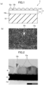
- FIG. 1(a) is a schematic sectional view depicting a metallic lustrous member with electromagnetic wave transmissibility (hereinafter referred to as “metallic lustrous member”) 1 according to one embodiment of the present invention, and an electromagnetic wave-transmissive metal film (hereinafter referred to as "metal film”) 3 using the metallic lustrous member
- FIG. 1(b) is an electron microscope photograph (SEM image) presenting a surface of the metallic lustrous member 1 according to this embodiment.
- SEM image electron microscope photograph
- an image size of the electron microscope photograph is 1.16 ⁇ m ⁇ 0.85 ⁇ m.
- the metallic lustrous member 1 comprises an indium oxide-containing layer 11 containing at least indium oxide and serving as an underlying layer, and a metal layer 12 laminated on the indium oxide-containing layer 11.
- the metal film 3 comprises the metallic lustrous member 1, and a substrate film 10.
- the indium oxide-containing layer 11 is provided on a surface of the substrate film 10 to be imparted with metallic luster.
- the indium oxide-containing layer 11 may be provided directly on the surface of the substrate film 10, or may be provided indirectly on the surface of the substrate film 10 through a protective film or the like provided on the surface of the substrate film 10.
- the indium oxide-containing layer 11 is provided on the surface of the substrate film 10 to be imparted with metallic luster, in a continuous state, i.e., without any gap therebetween.
- a continuous state it is possible to improve smoothness and corrosion resistance of the indium oxide-containing layer 11 and thus improve smoothness and corrosion resistance of the metallic lustrous member 1 and the metal film 3, and to facilitate forming the indium oxide-containing layer 11 without any in-plane variation.
- the metal layer 12 is laminated on the indium oxide-containing layer 11.
- the metal layer 12 includes a plurality of portions 12a. In a state in which the metal layer 12 is laminated on the indium oxide-containing layer 11, in at least part of the metal layer 12, the portions 12a are in a discontinuous state, i.e., in at least part of the metal layer 12, the portions 12a are separated from each other by a gap 12b. Because the portions 12a are separated from each other by the gap 12b, a sheet resistance in the portions 12a is increased, so that an interaction of the portions 12a with the electromagnetic wave is weakened to allow electromagnetic waves to be transmitted through the metal layer 12.
- Each of the portions 12a is an aggregate of sputtered particles formed by subjecting a metal to vapor deposition, sputtering or the like.
- a metal to vapor deposition, sputtering or the like.
- surface diffusibility of the particles on the substrate exerts an influence on the shape of the thin film.
- the present inventors have succeeded in allowing the metal layer to grow in a discontinuous state by providing the indium oxide-containing layer on the substrate to promote the surface diffusibility of the metal layer.
- the term "discontinuous state” means a state in which the portions 12a are separated from each other by the gap 12b, and therefore electrically insulated from each other.
- the configuration of the discontinuity is not particularly limited.
- it may include an island-shaped configuration and a cracked configuration.
- the term "island shape" means a structure in which the particles as the aggregate of the sputtered particles are independent of each other, and laid on the indium oxide-containing layer 11 in slightly spaced-apart relation to each other or in partially contact relation with each other, as presented in FIG. 1(b) .
- the substrate film 10 it is possible to use a transparent film made of a homopolymer or copolymer of polyethylene terephthalate (PET), polyethylene naphthalate (PEN), polybutylene terephthalate, polyamide, polyvinyl chloride, polycarbonate (PC), cycloolefin polymer (COP), polystyrene, polypropylene (PP), polyethylene, polycycloolefin, polyurethane, polymethylmethacrylate (PMMA), or ABS.
- PET polyethylene terephthalate
- PEN polyethylene naphthalate
- PC polycarbonate
- COP cycloolefin polymer
- PP polystyrene
- PP polypropylene
- PMMA polymethylmethacrylate
- ABS polymethylmethacrylate
- the transparent film is capable of withstanding high temperatures during vapor deposition, sputtering or the like.
- the transparent film is capable of withstanding high temperatures during vapor deposition, sputtering or the like.
- the transparent film is capable of withstanding high temperatures during vapor deposition, sputtering or the like.
- the transparent film is capable of withstanding high temperatures during vapor deposition, sputtering or the like.
- polyethylene terephthalate, polyethylene naphthalate, polymethylmethacrylate, polycarbonate, cycloolefin polymer, ABS, polypropylene, and polyurethane are preferable.
- polyethylene terephthalate, cycloolefin polymer, polycarbonate and polymethylmethacrylate are particularly preferable, because they have a good balance between heat resistance and cost.
- the substrate film 10 may be a single-layer film or may be a laminate film. From a viewpoint of processability and the like, the thickness thereof is preferably from about 6 to 250
- the substrate film 10 is merely one example of an object on which the metallic lustrous member 1 according to the present invention can be provided (this object will hereinafter be referred to as "substrate").
- the substrate includes a resin molded substrate, a glass substrate, and an article body to be imparted with metallic luster.
- the resin molded substrate include a resin substrate for an emblem of an automotive vehicle.
- the article body to be imparted with metallic luster includes a body of a door knob of an automotive vehicle using a smart key, and a housing (outer casing) of a mobile phone, a personal computer, a refrigerator or the like.
- the metallic lustrous member 1 according to the present invention can be provided on any of the above substrates.
- the substrate to be provided with the metallic lustrous member 1 preferably has the similar material to that of or satisfies the similar requirements to those of the above substrate film 10.
- the indium oxide-containing layer 11 As a material for the indium oxide-containing layer 11, it is possible to use indium oxide (In 2 O 3 ) itself, or a metal-containing substance such as indium tin oxide (ITO) or indium zinc oxide (IZO). Among them, ITO and IZO containing the second metal are more preferable in that they have high discharge stability in a sputtering process.
- ITO and IZO containing the second metal are more preferable in that they have high discharge stability in a sputtering process.
- the indium oxide-containing layer 11 it becomes possible to form a continuous film along the surface of the substrate. In this case, it also becomes possible to laminate the metal layer on the indium oxide-containing layer, in e.g., an island-shaped discontinuous structure.
- the metal layer As a material for the metal layer, it becomes possible to use not only chromium (Cr) or indium (In) but also any of some other metals such as aluminum, which have been hardly used as the material because they normally have difficulty in being formed into a discontinuous structure, as described in more detail later.
- the content rate by weight of tin (Sn) to In 2 O 3 in ITO is not particularly limited. For example, it may be from 2.5 wt% to 30 wt%, preferably from 3 wt% to 10 wt%. Further, for example, the content rate by weight of zinc oxide (ZnO) to In 2 O 3 in IZO is may be from 2 wt% to 20 wt%.
- the thickness of the indium oxide-containing layer 11 is generally preferably 1000 nm or less, more preferably 50 nm or less, still more preferably 20 nm or less.
- the thickness of the indium oxide-containing layer 11 is preferably 1 nm or more, and, from a viewpoint of reliably obtaining the discontinuous state, it is more preferably 2 nm or more.
- the metal layer 12 is essentially capable of bringing out sufficient lustrousness. Further, it is desirable that the melting point thereof is relatively low. This is because the metal layer 12 is created through thin-film growth using sputtering. For this reason, a metal having a melting point of about 1000°C or less is suitable as a material for the metal layer 12.
- the metal layer 12 is made of at least one metal selected from the group consisting of aluminum (Al), and optionally zinc (Zn), lead (Pb), copper (Cu) and silver (Ag).
- the thickness of the metal layer 12 is generally 20 nm or more.
- the thickness of the metal layer 12 is generally 100 nm or less.
- the thickness of the metal layer 12 is from 20 nm to 100 nm, more preferably from 30 nm to 70 nm. This thickness range is suited to forming a uniform film with good productivity, and can provide good appearance of a resin molded article as a final product.
- the ratio of the thickness of the metal layer to the thickness of the indium oxide-containing layer is preferably from 0.1 to 100, preferably from 0.3 to 35.
- a laminate of the metal layer and the indium oxide-containing layer has a sheet resistance of 100 to 100,000 ⁇ / ⁇ .
- the electromagnetic wave transmissibility of the laminate at a wavelength of 1 GHz is from about 10 to 0.01 [- dB]. More preferably, the sheet resistance is from 1,000 to 50,000 ⁇ / ⁇ .
- the value of the sheet resistance is largely influenced by not only the material and thickness of the metal layer but also the material and thickness of the indium oxide-containing layer serving as an underlying layer. Therefore, the value of the sheet resistance needs to be set while taking into account the relationship with the indium oxide-containing layer.
- the metal layer 11 is formed on the substrate 10 in a continuous state. In this case, although sufficient lustrousness can be obtained, the sheet resistance becomes significantly small, so that it is impossible to ensure the electromagnetic wave transmissibility. Differently, in the case where the metal layer 12 is laminated on the indium oxide-containing layer 11 formed on the substrate, the metal layer 11 is formed, in a discontinuous state, e.g., on the indium oxide-containing layer 11 formed in a continuous state, so that it is of course possible to obtain sufficient lustrousness and also possible to ensure the electromagnetic wave transmissibility.
- the metal layer 11 is not exactly clear, it is inferred as follows. That is, in a thin film forming process for the metal layer 11, easiness in forming a discontinuous structure of the metal layer 11 is relevant to surface diffusibility of the metal layer 11 on a to-be-coated member (in this embodiment, the indium oxide-containing layer 11) to be coated with the metal layer 11. Specifically, the discontinuous structure is more likely to be formed under the condition that: the temperature of the to-be-coated member is higher; the wettability of the metal layer with respect to the to-be-coated member is smaller; and the melting point of the metal layer is lower.
- the discontinuous structure is considered to be able to be formed in the similar manner.
- the metallic lustrous member 1 One example of a production method for the metallic lustrous member 1 will be described by taking an example in which the substrate film 10 is used as the substrate, i.e., the metal film 3 is produced. Although not particularly described, a metallic lustrous member using the substrate other than the substrate film 10 can also be produced by the similar method.
- the indium oxide-containing layer 11 is formed onto the substrate film 10.
- the indium oxide-containing layer 11 can be formed by vacuum deposition, sputtering, ion plating or the like. Among them, sputtering is preferable, from a viewpoint of being capable of strictly controlling the thickness of the indium oxide-containing layer 11 even when it has a relatively large area.
- the metal later 12 is laminated to the indium oxide-containing layer 11.
- sputtering can be used.
- the metal layer 12 is laminated such that it comes into direct contact with the indium oxide-containing layer 11 without interposing any additional layer therebetween.
- an additional layer may be interposed therebetween.
- the present invention will be more specifically described below by taking inventive examples and comparative examples.
- Various samples of the metal film 3 were prepared, and evaluated in terms of sheet resistance, electromagnetic wave transmission attenuation amount, and visible light reflectance.
- the sheet resistance and the electromagnetic wave transmission attenuation amount are evaluation indexes of the electromagnetic wave transmissibility
- the visible light reflectance is an evaluation index of the lustrousness. A larger value of each of the visible light reflectance and the sheet resistance is more desirable, and a smaller value of the electromagnetic wave transmission attenuation amount is more desirable.
- the sheet resistance was measured by an eddy-current measurement method in accordance with JIS-Z2316, using a non-contact type resistance measuring device NC-80MAP manufactured by Napson Corporation.
- This sheet resistance needs to be equal to or greater than 100 ⁇ / ⁇ , preferably equal to or greater than 200 ⁇ / ⁇ , more preferably equal to or greater than 600 ⁇ / ⁇ . If the sheet resistance is less than 100 ⁇ / ⁇ , there is a problem that a sufficient electromagnetic wave transmissibility cannot be obtained.
- An electromagnetic wave transmission attenuation amount at 1 GHz was evaluated using a KEC method measurement and evaluation jig, and a spectral analyzer CXA signal Analyzer NA9000A manufactured by Agilent technologies Inc.
- An electromagnetic wave transmissibility in a frequency band (76 to 80 GHz) of a millimeter-wave radar is correlated with an electromagnetic wave transmissibility in a microwave band (1 GHz), and thus they exhibit relatively close values.
- the electromagnetic wave transmissibility i.e., microwave electric field transmission attenuation amount, in the microwave microwave band (1 GHz) was used as an index.
- This microwave electric field transmission attenuation amount needs to be equal to or less than 10 [- dB], preferably, equal to or less than 5 [- dB], more preferably equal to or less than 2 [- dB]. If the electromagnetic wave transmission attenuation amount is equal to or greater than 10 [- dB], there is a problem that 90% or more of an electromagnetic wave is shielded.
- a reflectance at a measurement wavelength of 550 nm was measured using a spectrophotometer U4100 manufactured by Hitachi High Technologies Co., Ltd.
- the reflectance of an Al-deposited mirror was defined as a reflectance of 100%.
- the visible light reflectance need to be equal to or greater than 20%, preferably equal to or greater than 40%, more preferably equal to or greater than 50%. If the visible light reflectance is less than 20%, there is a problem that the lustrousness significantly deteriorates, resulting in failing to ensure excellent external appearance.
- the ITO is a composition obtained by adding Sn to In 2 O 3 in an amount of 10 wt%.
- a 50 nm-thick aluminum (Al) layer was formed on the ITO layer to obtain a metallic lustrous member (metal film).
- the temperature of the substrate film during formation of the Al layer was set at 130°C.
- FIG. 1(b) is an electron microscope photograph (SEM image) of a surface of the metallic lustrous member (metal film) obtained as a result of the above process
- FIG. 2 is an image of a cut surface in a partial region of FIG. 1(b) .
- an image size of the electron microscope photograph in FIG. 2 is 1.16 ⁇ m ⁇ 0.85 ⁇ m.
- the ITO layer of the metallic lustrous member is provided along the surface of the substrate film in a continuous state, so that high smoothness and corrosion resistance could be obtained
- the aluminum layer laminated on the ITO layer includes a plurality of portions 12a formed in a discontinuous state, so that the sheet resistance was 260 ⁇ / ⁇ , and the electromagnetic wave transmission attenuation amount at a wavelength of 1GHz was 4.5 [- dB], i.e., in terms of the electromagnetic wave transmissibility, a good result could be obtained.
- the visible light reflectance of the metallic lustrous member was 56%, i.e., in terms of the visible light reflectance, a good result could be obtained.
- Table 1 with regard to a result of "evaluation" of the visible light reflectance, when the visible light reflectance is greater than 50%, the lustrousness was evaluated as " ⁇ ", and, when the visible light reflectance is from 50% to greater than 40%, the lustrousness was evaluated as "O". Further, when the visible light reflectance is from 40% to greater than 20%, the lustrousness was evaluated as " ⁇ ", and, when the visible light reflectance is 20% or less, the lustrousness was evaluated as " ⁇ ".
- the thickness of the ITO layer was changed to a smaller value than that in Inventive Example 1.
- the remaining conditions were the same as those in Inventive Example 1.
- the content rate of Sn in the ITO layer was changed to a larger value than that in Inventive Example 1.
- the content rate was changed to a smaller value than that in Inventive Example 1.
- the content rate of Sn in the ITO layer is set to zero.
- this layer is not an ITO layer but an indium oxide (In 2 O 3 ) layer.
- the thickness of the aluminum layer was set to 40 nm. The remaining conditions were the same as those in Inventive Example 1.
- IZO As a material for the indium oxide-containing layer, IZO obtained by adding ZnO to indium oxide was used, instead of ITO. ZnO is added to In 2 O 3 in an amount of 11 wt%. The remaining conditions were the same as those in Inventive Example 1.
- the thickness of the aluminum layer laminated on the ITO layer was changed to a larger value than that in Inventive Example 1.
- the remaining conditions were the same as those in Inventive Example 1.
- the aluminum layer was formed directly on the substrate film without providing any ITO layer.
- the remaining conditions were the same as those in Inventive Example 1.
- the metal layer 12 formed in the metallic lustrous member 1 has a small thickness of about 20 to 100 nm, and can be used by itself as a metal thin film.
- the metal layer 12 may be formed on the indium oxide-containing layer 11 laminated on a substrate such as the substrate film 10 by sputtering to obtain a film. Further, separately from this, an adhesive is applied onto a substrate to produce an adhesive layer-attached substrate. Then, the film is laminated to the adhesive layer-attached substrate, such that the metal layer 12 comes in contact with the adhesive layer.
- the metal layer (metal thin film) 12 which has been located on the outermost surface side of the film can be transferred to the outermost surface side of the adhesive layer-attached substrate, by separating the film and the substrate from each other, after fully having contacted them.
- the metal film or the metallic lustrous member according to the present invention can be suitably used, e.g., to decorate a cover member of a millimeter-wave radar mounted to a front component such as a front grille or an emblem at a front end of an automotive vehicle.
- the present invention may also be applied to various other articles requiring both an aesthetic quality and electromagnetic wave transmissibility, such as a mobile phone, a smart phone, a tablet PC, a notebook PC, and a refrigerator.
Landscapes
- Chemical & Material Sciences (AREA)
- Engineering & Computer Science (AREA)
- Chemical Kinetics & Catalysis (AREA)
- Materials Engineering (AREA)
- Mechanical Engineering (AREA)
- Metallurgy (AREA)
- Organic Chemistry (AREA)
- Inorganic Chemistry (AREA)
- Ceramic Engineering (AREA)
- Laminated Bodies (AREA)
- Shielding Devices Or Components To Electric Or Magnetic Fields (AREA)
- Physical Vapour Deposition (AREA)
Applications Claiming Priority (2)
| Application Number | Priority Date | Filing Date | Title |
|---|---|---|---|
| JP2016208000A JP6400062B2 (ja) | 2016-10-24 | 2016-10-24 | 電磁波透過性金属光沢部材、これを用いた物品、及び、金属薄膜 |
| PCT/JP2017/038354 WO2018079547A1 (ja) | 2016-10-24 | 2017-10-24 | 電磁波透過性金属光沢部材、これを用いた物品、及び、金属薄膜 |
Publications (3)
| Publication Number | Publication Date |
|---|---|
| EP3536495A1 EP3536495A1 (en) | 2019-09-11 |
| EP3536495A4 EP3536495A4 (en) | 2020-05-13 |
| EP3536495B1 true EP3536495B1 (en) | 2025-05-21 |
Family
ID=62023596
Family Applications (1)
| Application Number | Title | Priority Date | Filing Date |
|---|---|---|---|
| EP17865289.7A Active EP3536495B1 (en) | 2016-10-24 | 2017-10-24 | Electromagnetic wave-permeable shiny metal member, article using same, and metal thin film |
Country Status (7)
Families Citing this family (32)
| Publication number | Priority date | Publication date | Assignee | Title |
|---|---|---|---|---|
| JP6980537B2 (ja) * | 2018-01-12 | 2021-12-15 | 株式会社ウェーブロック・アドバンスト・テクノロジー | 金属層保持用フィルム、金属調加飾シート中間体、金属調加飾シート、押出ラミネート体、金属調成形体、射出成形体、金属調成形体の製造方法、射出成形体の製造方法および押出ラミネート体の製造方法 |
| JP7516707B2 (ja) * | 2018-01-12 | 2024-07-17 | 日東電工株式会社 | 電波透過性金属光沢部材、これを用いた物品、及びその製造方法 |
| WO2019139156A1 (ja) * | 2018-01-12 | 2019-07-18 | 日東電工株式会社 | 積層体 |
| WO2019139122A1 (ja) * | 2018-01-12 | 2019-07-18 | 日東電工株式会社 | 電波透過性金属光沢部材、これを用いた物品、及びその製造方法 |
| WO2019208499A1 (ja) * | 2018-04-23 | 2019-10-31 | 日東電工株式会社 | 電磁波透過性金属光沢物品 |
| WO2019208494A1 (ja) * | 2018-04-23 | 2019-10-31 | 日東電工株式会社 | 電磁波透過性金属光沢物品、及び、金属薄膜 |
| CN112004666A (zh) * | 2018-04-23 | 2020-11-27 | 日东电工株式会社 | 电磁波透过性金属光泽物品 |
| JP7319080B2 (ja) * | 2018-04-23 | 2023-08-01 | 日東電工株式会社 | 電磁波透過性金属光沢物品、及び、金属薄膜 |
| WO2019208504A1 (ja) * | 2018-04-23 | 2019-10-31 | 日東電工株式会社 | 電磁波透過性金属光沢物品、及び、金属薄膜 |
| JP2019188809A (ja) * | 2018-04-23 | 2019-10-31 | 日東電工株式会社 | 電磁波透過性金属光沢物品 |
| WO2019208489A1 (ja) * | 2018-04-23 | 2019-10-31 | 日東電工株式会社 | 電磁波透過性金属光沢物品 |
| JP7319079B2 (ja) * | 2018-04-23 | 2023-08-01 | 日東電工株式会社 | 電磁波透過性金属光沢物品、及び、加飾部材 |
| JP7319077B2 (ja) * | 2018-04-23 | 2023-08-01 | 日東電工株式会社 | 電磁波透過性金属光沢物品、及び、金属薄膜 |
| JPWO2019208490A1 (ja) * | 2018-04-23 | 2021-05-13 | 日東電工株式会社 | 電磁波透過性金属光沢物品及びその製造方法 |
| WO2019208488A1 (ja) * | 2018-04-23 | 2019-10-31 | 日東電工株式会社 | 電磁波透過性金属光沢物品 |
| WO2019208493A1 (ja) * | 2018-04-23 | 2019-10-31 | 日東電工株式会社 | 電磁波透過性金属光沢物品、及び、加飾部材 |
| CN112020424A (zh) * | 2018-04-23 | 2020-12-01 | 日东电工株式会社 | 电磁波透过性金属光泽物品 |
| WO2019230955A1 (ja) * | 2018-06-01 | 2019-12-05 | 大日本印刷株式会社 | 金属調加飾用部材及びそれを用いた金属調加飾成形体 |
| WO2020067052A1 (ja) * | 2018-09-25 | 2020-04-02 | 積水化学工業株式会社 | 電波透過体 |
| JP7101634B2 (ja) * | 2019-03-29 | 2022-07-15 | 本田技研工業株式会社 | 樹脂成形品 |
| WO2020255383A1 (ja) * | 2019-06-21 | 2020-12-24 | 昭和電工マテリアルズ株式会社 | 装飾品 |
| JP2021024251A (ja) * | 2019-08-08 | 2021-02-22 | 日東電工株式会社 | 電磁波透過性積層体 |
| WO2021065840A1 (ja) * | 2019-09-30 | 2021-04-08 | 日東電工株式会社 | 積層体及び物品 |
| US12249761B2 (en) * | 2019-10-15 | 2025-03-11 | Motherson Innovations Company Limited | First surface decorative element |
| JP7647582B2 (ja) * | 2019-12-26 | 2025-03-18 | 大日本印刷株式会社 | 金属調加飾シート及びこれを備える金属調加飾成形体 |
| EP4082775A4 (en) * | 2019-12-27 | 2024-01-24 | Dai Nippon Printing Co., Ltd. | METAL FINISH DECORATIVE SHEET AND METAL FINISH DECORATIVE MOLDED BODY COMPRISING METAL FINISH DECORATIVE SHEET |
| JP7670682B2 (ja) * | 2020-03-09 | 2025-04-30 | 日東電工株式会社 | 電磁波透過性積層部材、及びその製造方法 |
| JP7670684B2 (ja) * | 2020-03-17 | 2025-04-30 | 日東電工株式会社 | 電磁波透過性金属光沢部材 |
| JP2023076328A (ja) | 2021-11-22 | 2023-06-01 | スタンレー電気株式会社 | ランプ装置 |
| EP4431983A1 (en) | 2021-12-21 | 2024-09-18 | Stanley Electric Co. Ltd. | Detecting module, and lamp device and lamp system provided with detecting module |
| JP7582243B2 (ja) | 2022-04-14 | 2024-11-13 | トヨタ自動車株式会社 | 電波透過性金属調部材及びその製造方法 |
| CN115074666B (zh) * | 2022-06-13 | 2023-11-03 | 桂林电子科技大学 | 一种多层复合ito薄膜的制备方法 |
Family Cites Families (28)
| Publication number | Priority date | Publication date | Assignee | Title |
|---|---|---|---|---|
| JP3476277B2 (ja) * | 1995-02-16 | 2003-12-10 | 三井化学株式会社 | 透明導電性積層体 |
| JPH11268183A (ja) * | 1998-03-19 | 1999-10-05 | Mitsui Chem Inc | ポリイミド−金属積層体およびその製造方法 |
| JP2001329363A (ja) * | 2000-05-18 | 2001-11-27 | Bridgestone Corp | 積層膜の形成方法及び積層膜 |
| JP4099946B2 (ja) * | 2001-01-11 | 2008-06-11 | 株式会社ファルテック | 金属光輝色を呈する成形品の製造方法 |
| JP3568493B2 (ja) * | 2001-06-18 | 2004-09-22 | 日本写真印刷株式会社 | 赤外線透過カバーパネル、赤外線透過カバーパネル用加飾シート |
| JP4667923B2 (ja) * | 2005-03-25 | 2011-04-13 | トヨタ自動車株式会社 | レーダ装置ビーム経路内用光輝装飾成形品 |
| JP4657070B2 (ja) * | 2005-09-27 | 2011-03-23 | 豊田合成株式会社 | レーダー装置カバー及びその製造方法 |
| JP4706596B2 (ja) | 2005-10-31 | 2011-06-22 | 豊田合成株式会社 | 樹脂製品及びその製造方法並びに金属皮膜の成膜方法 |
| JP4732147B2 (ja) * | 2005-11-21 | 2011-07-27 | 豊田合成株式会社 | 樹脂製品及びその製造方法並びに金属皮膜の成膜方法 |
| JP2008080712A (ja) | 2006-09-28 | 2008-04-10 | Toyoda Gosei Co Ltd | 光輝性及び不連続構造の金属皮膜を有する樹脂製品 |
| JP2009298006A (ja) | 2008-06-12 | 2009-12-24 | Toyoda Gosei Co Ltd | 電磁波透過性光輝樹脂製品及び製造方法 |
| JP2010005999A (ja) | 2008-06-30 | 2010-01-14 | Nissha Printing Co Ltd | クラックを有する金属膜加飾シートの製造方法 |
| CN102405421B (zh) * | 2009-02-27 | 2013-11-13 | 丰田自动车株式会社 | 车载雷达装置以及车载雷达装置用罩 |
| JP2011025634A (ja) * | 2009-07-29 | 2011-02-10 | Mitsubishi Electric Corp | 電磁波透過性加飾部品 |
| US8280594B2 (en) | 2009-09-28 | 2012-10-02 | Aisin Seiki Kabushiki Kaisha | Door opening/closing apparatus and coating film forming method |
| WO2011090010A1 (ja) | 2010-01-25 | 2011-07-28 | 東レフィルム加工株式会社 | 金属薄膜転写材料およびその製造方法 |
| JP5390427B2 (ja) | 2010-02-09 | 2014-01-15 | 関東化成工業株式会社 | 電磁波透過用金属被膜、電磁波透過用金属被膜の形成方法及び車載用レーダー装置 |
| KR101116375B1 (ko) * | 2010-06-21 | 2012-03-16 | 한국과학기술원 | 접착성의 금속필름 제조방법 및 그 금속필름 |
| JP5375855B2 (ja) * | 2011-02-22 | 2013-12-25 | トヨタ自動車株式会社 | 装飾被膜 |
| JP5817195B2 (ja) * | 2011-04-19 | 2015-11-18 | アイシン精機株式会社 | ドア開閉装置 |
| US20150293025A1 (en) * | 2012-12-18 | 2015-10-15 | Toray Industries Inc. | Metal dot substrate and method of manufacturing metal dot substrate |
| WO2014126135A1 (ja) * | 2013-02-13 | 2014-08-21 | 東洋紡株式会社 | 熱線反射電波透過透明積層体 |
| FR3009833B1 (fr) * | 2013-08-20 | 2015-10-16 | Saint Gobain | Procede d'obtention d'un substrat muni d'un revetement comprenant une couche mince metallique discontinue |
| JPWO2015025963A1 (ja) * | 2013-08-23 | 2017-03-02 | 王子ホールディングス株式会社 | 熱線遮蔽材 |
| JP2015182334A (ja) * | 2014-03-25 | 2015-10-22 | 東レ株式会社 | 金属ドット基板およびその製造方法 |
| JP6409588B2 (ja) * | 2015-01-21 | 2018-10-24 | Tdk株式会社 | 透明導電体及びタッチパネル |
| JP2016144930A (ja) | 2015-02-03 | 2016-08-12 | 王子ホールディングス株式会社 | 遮熱フィルム、遮熱合わせガラス、遮熱フィルムの製造方法および遮熱合わせガラスの製造方法 |
| WO2016125823A1 (ja) * | 2015-02-03 | 2016-08-11 | 王子ホールディングス株式会社 | 遮熱フィルム、遮熱合わせガラスおよびその製造方法 |
-
2016
- 2016-10-24 JP JP2016208000A patent/JP6400062B2/ja active Active
-
2017
- 2017-10-24 KR KR1020217011568A patent/KR20210045527A/ko not_active Ceased
- 2017-10-24 KR KR1020197014865A patent/KR20190061091A/ko not_active Ceased
- 2017-10-24 TW TW106136432A patent/TWI791466B/zh active
- 2017-10-24 KR KR1020197014909A patent/KR102271407B1/ko active Active
- 2017-10-24 WO PCT/JP2017/038354 patent/WO2018079547A1/ja active IP Right Grant
- 2017-10-24 US US16/344,754 patent/US11383478B2/en active Active
- 2017-10-24 EP EP17865289.7A patent/EP3536495B1/en active Active
- 2017-10-24 CN CN201780065919.0A patent/CN109890608A/zh active Pending
Also Published As
| Publication number | Publication date |
|---|---|
| KR102271407B1 (ko) | 2021-06-30 |
| JP2018069462A (ja) | 2018-05-10 |
| TW201827214A (zh) | 2018-08-01 |
| JP6400062B2 (ja) | 2018-10-03 |
| KR20190062604A (ko) | 2019-06-05 |
| KR20190061091A (ko) | 2019-06-04 |
| EP3536495A4 (en) | 2020-05-13 |
| EP3536495A1 (en) | 2019-09-11 |
| TWI791466B (zh) | 2023-02-11 |
| WO2018079547A1 (ja) | 2018-05-03 |
| KR20210045527A (ko) | 2021-04-26 |
| US11383478B2 (en) | 2022-07-12 |
| CN109890608A (zh) | 2019-06-14 |
| US20190275759A1 (en) | 2019-09-12 |
Similar Documents
| Publication | Publication Date | Title |
|---|---|---|
| EP3536495B1 (en) | Electromagnetic wave-permeable shiny metal member, article using same, and metal thin film | |
| US11577491B2 (en) | Metallic lustrous member with radio wave transmissibility, article using same, and production method therefor | |
| JP7319077B2 (ja) | 電磁波透過性金属光沢物品、及び、金属薄膜 | |
| WO2019208504A1 (ja) | 電磁波透過性金属光沢物品、及び、金属薄膜 | |
| JP6944425B2 (ja) | 電磁波透過性金属光沢部材、これを用いた物品、及び、金属薄膜 | |
| WO2019208499A1 (ja) | 電磁波透過性金属光沢物品 | |
| WO2021182380A1 (ja) | 電磁波透過性積層部材、及びその製造方法 | |
| JP7319081B2 (ja) | 電磁波透過性金属光沢物品 | |
| TW202003217A (zh) | 電磁波透過性金屬光澤物品 | |
| JP7319080B2 (ja) | 電磁波透過性金属光沢物品、及び、金属薄膜 | |
| JP7319078B2 (ja) | 電磁波透過性金属光沢物品 | |
| WO2019139122A1 (ja) | 電波透過性金属光沢部材、これを用いた物品、及びその製造方法 | |
| WO2019208494A1 (ja) | 電磁波透過性金属光沢物品、及び、金属薄膜 | |
| WO2019208488A1 (ja) | 電磁波透過性金属光沢物品 | |
| WO2019208490A1 (ja) | 電磁波透過性金属光沢物品及びその製造方法 | |
| WO2019208489A1 (ja) | 電磁波透過性金属光沢物品 |
Legal Events
| Date | Code | Title | Description |
|---|---|---|---|
| STAA | Information on the status of an ep patent application or granted ep patent |
Free format text: STATUS: THE INTERNATIONAL PUBLICATION HAS BEEN MADE |
|
| PUAI | Public reference made under article 153(3) epc to a published international application that has entered the european phase |
Free format text: ORIGINAL CODE: 0009012 |
|
| STAA | Information on the status of an ep patent application or granted ep patent |
Free format text: STATUS: REQUEST FOR EXAMINATION WAS MADE |
|
| 17P | Request for examination filed |
Effective date: 20190502 |
|
| AK | Designated contracting states |
Kind code of ref document: A1 Designated state(s): AL AT BE BG CH CY CZ DE DK EE ES FI FR GB GR HR HU IE IS IT LI LT LU LV MC MK MT NL NO PL PT RO RS SE SI SK SM TR |
|
| AX | Request for extension of the european patent |
Extension state: BA ME |
|
| DAV | Request for validation of the european patent (deleted) | ||
| DAX | Request for extension of the european patent (deleted) | ||
| A4 | Supplementary search report drawn up and despatched |
Effective date: 20200409 |
|
| RIC1 | Information provided on ipc code assigned before grant |
Ipc: B32B 3/14 20060101ALI20200403BHEP Ipc: C23C 14/34 20060101ALI20200403BHEP Ipc: B32B 9/00 20060101AFI20200403BHEP Ipc: C23C 14/08 20060101ALI20200403BHEP Ipc: C23C 14/14 20060101ALI20200403BHEP Ipc: C23C 28/00 20060101ALI20200403BHEP Ipc: C23C 14/18 20060101ALI20200403BHEP |
|
| STAA | Information on the status of an ep patent application or granted ep patent |
Free format text: STATUS: EXAMINATION IS IN PROGRESS |
|
| 17Q | First examination report despatched |
Effective date: 20220523 |
|
| GRAP | Despatch of communication of intention to grant a patent |
Free format text: ORIGINAL CODE: EPIDOSNIGR1 |
|
| STAA | Information on the status of an ep patent application or granted ep patent |
Free format text: STATUS: GRANT OF PATENT IS INTENDED |
|
| RIC1 | Information provided on ipc code assigned before grant |
Ipc: C23C 14/02 20060101ALI20241202BHEP Ipc: C23C 14/34 20060101ALI20241202BHEP Ipc: C23C 14/18 20060101ALI20241202BHEP Ipc: C23C 14/14 20060101ALI20241202BHEP Ipc: C23C 14/08 20060101ALI20241202BHEP Ipc: C23C 28/00 20060101ALI20241202BHEP Ipc: B32B 3/14 20060101ALI20241202BHEP Ipc: B32B 9/00 20060101AFI20241202BHEP |
|
| INTG | Intention to grant announced |
Effective date: 20241219 |
|
| P01 | Opt-out of the competence of the unified patent court (upc) registered |
Free format text: CASE NUMBER: APP_3164/2025 Effective date: 20250120 |
|
| GRAS | Grant fee paid |
Free format text: ORIGINAL CODE: EPIDOSNIGR3 |
|
| GRAA | (expected) grant |
Free format text: ORIGINAL CODE: 0009210 |
|
| STAA | Information on the status of an ep patent application or granted ep patent |
Free format text: STATUS: THE PATENT HAS BEEN GRANTED |
|
| AK | Designated contracting states |
Kind code of ref document: B1 Designated state(s): AL AT BE BG CH CY CZ DE DK EE ES FI FR GB GR HR HU IE IS IT LI LT LU LV MC MK MT NL NO PL PT RO RS SE SI SK SM TR |
|
| REG | Reference to a national code |
Ref country code: GB Ref legal event code: FG4D |
|
| REG | Reference to a national code |
Ref country code: CH Ref legal event code: EP |
|
| REG | Reference to a national code |
Ref country code: DE Ref legal event code: R096 Ref document number: 602017089604 Country of ref document: DE |
|
| REG | Reference to a national code |
Ref country code: IE Ref legal event code: FG4D |