WO2021182380A1 - 電磁波透過性積層部材、及びその製造方法 - Google Patents
電磁波透過性積層部材、及びその製造方法 Download PDFInfo
- Publication number
- WO2021182380A1 WO2021182380A1 PCT/JP2021/008947 JP2021008947W WO2021182380A1 WO 2021182380 A1 WO2021182380 A1 WO 2021182380A1 JP 2021008947 W JP2021008947 W JP 2021008947W WO 2021182380 A1 WO2021182380 A1 WO 2021182380A1
- Authority
- WO
- WIPO (PCT)
- Prior art keywords
- indium oxide
- containing layer
- electromagnetic wave
- layer
- laminated member
- Prior art date
Links
Images


Classifications
-
- B—PERFORMING OPERATIONS; TRANSPORTING
- B32—LAYERED PRODUCTS
- B32B—LAYERED PRODUCTS, i.e. PRODUCTS BUILT-UP OF STRATA OF FLAT OR NON-FLAT, e.g. CELLULAR OR HONEYCOMB, FORM
- B32B15/00—Layered products comprising a layer of metal
- B32B15/04—Layered products comprising a layer of metal comprising metal as the main or only constituent of a layer, which is next to another layer of the same or of a different material
-
- B—PERFORMING OPERATIONS; TRANSPORTING
- B32—LAYERED PRODUCTS
- B32B—LAYERED PRODUCTS, i.e. PRODUCTS BUILT-UP OF STRATA OF FLAT OR NON-FLAT, e.g. CELLULAR OR HONEYCOMB, FORM
- B32B3/00—Layered products comprising a layer with external or internal discontinuities or unevennesses, or a layer of non-planar form; Layered products having particular features of form
- B32B3/10—Layered products comprising a layer with external or internal discontinuities or unevennesses, or a layer of non-planar form; Layered products having particular features of form characterised by a discontinuous layer, i.e. formed of separate pieces of material
-
- B—PERFORMING OPERATIONS; TRANSPORTING
- B32—LAYERED PRODUCTS
- B32B—LAYERED PRODUCTS, i.e. PRODUCTS BUILT-UP OF STRATA OF FLAT OR NON-FLAT, e.g. CELLULAR OR HONEYCOMB, FORM
- B32B9/00—Layered products comprising a layer of a particular substance not covered by groups B32B11/00 - B32B29/00
-
- C—CHEMISTRY; METALLURGY
- C23—COATING METALLIC MATERIAL; COATING MATERIAL WITH METALLIC MATERIAL; CHEMICAL SURFACE TREATMENT; DIFFUSION TREATMENT OF METALLIC MATERIAL; COATING BY VACUUM EVAPORATION, BY SPUTTERING, BY ION IMPLANTATION OR BY CHEMICAL VAPOUR DEPOSITION, IN GENERAL; INHIBITING CORROSION OF METALLIC MATERIAL OR INCRUSTATION IN GENERAL
- C23C—COATING METALLIC MATERIAL; COATING MATERIAL WITH METALLIC MATERIAL; SURFACE TREATMENT OF METALLIC MATERIAL BY DIFFUSION INTO THE SURFACE, BY CHEMICAL CONVERSION OR SUBSTITUTION; COATING BY VACUUM EVAPORATION, BY SPUTTERING, BY ION IMPLANTATION OR BY CHEMICAL VAPOUR DEPOSITION, IN GENERAL
- C23C14/00—Coating by vacuum evaporation, by sputtering or by ion implantation of the coating forming material
- C23C14/06—Coating by vacuum evaporation, by sputtering or by ion implantation of the coating forming material characterised by the coating material
- C23C14/08—Oxides
-
- C—CHEMISTRY; METALLURGY
- C23—COATING METALLIC MATERIAL; COATING MATERIAL WITH METALLIC MATERIAL; CHEMICAL SURFACE TREATMENT; DIFFUSION TREATMENT OF METALLIC MATERIAL; COATING BY VACUUM EVAPORATION, BY SPUTTERING, BY ION IMPLANTATION OR BY CHEMICAL VAPOUR DEPOSITION, IN GENERAL; INHIBITING CORROSION OF METALLIC MATERIAL OR INCRUSTATION IN GENERAL
- C23C—COATING METALLIC MATERIAL; COATING MATERIAL WITH METALLIC MATERIAL; SURFACE TREATMENT OF METALLIC MATERIAL BY DIFFUSION INTO THE SURFACE, BY CHEMICAL CONVERSION OR SUBSTITUTION; COATING BY VACUUM EVAPORATION, BY SPUTTERING, BY ION IMPLANTATION OR BY CHEMICAL VAPOUR DEPOSITION, IN GENERAL
- C23C14/00—Coating by vacuum evaporation, by sputtering or by ion implantation of the coating forming material
- C23C14/06—Coating by vacuum evaporation, by sputtering or by ion implantation of the coating forming material characterised by the coating material
- C23C14/14—Metallic material, boron or silicon
Definitions
- the present invention relates to an electromagnetic wave transmitting laminated member and a method for manufacturing the same.
- a member having electromagnetic wave transmission and metallic luster has both a high-class appearance derived from the metallic luster and electromagnetic wave transmission, and is therefore suitably used for an apparatus for transmitting and receiving electromagnetic waves.
- Such an electromagnetic wave transmissive laminated member is a device for transmitting and receiving electromagnetic waves, and is used for various devices that require communication, for example, an automobile door handle provided with a smart key, an in-vehicle communication device, a mobile phone, a personal computer, and other electronic devices. It is expected to be applied to such applications. Furthermore, in recent years, with the development of IoT technology, it is expected to be applied in a wide range of fields such as home appliances such as refrigerators and household appliances, which have not been used for communication in the past.
- Patent Document 1 includes an indium oxide-containing layer provided on the surface of a substrate and a metal layer laminated on the indium oxide-containing layer, and the metal layer is at least partially provided. Described is an electromagnetic wave transmissive metallic luster member comprising a plurality of portions that are discontinuous with each other.
- the metal layer in the electromagnetic wave transmitting laminated member of the prior art could be formed only to a thickness of about 50 nm, although it depends on the forming method and the type of the substrate. If the thickness is larger than that, the metal formed in an island shape overlaps with each other, and the resistance value sharply decreases, so that the electromagnetic wave transmission is significantly impaired. Therefore, regarding the thickness of the metal layer, it is necessary to control the film thickness on the order of several nanometers, which makes stable production difficult and causes a problem that the yield is lowered.
- the present invention has been made to solve the above problems in the prior art, and provides an electromagnetic wave transmitting laminated member having excellent electromagnetic wave transmission and capable of controlling the thickness of a metal layer in a wide range.
- the purpose is.
- the present inventors have found that the above problems can be solved by setting the oxygen concentration in the indium oxide-containing layer within a specific range, and have completed the present invention. rice field.
- the present invention is as follows. [1] A substrate, an indium oxide-containing layer formed on the substrate, and a metal layer formed on the indium oxide-containing layer are provided.
- the metal layer contains a plurality of portions that are discontinuous with each other, at least in part.
- the oxygen atom ratio (O / (In + M) ratio) to the total of the indium atom and at least one metal atom M of Sn and Zn when the surface of the indium oxide-containing layer is measured by X-ray photoelectron spectroscopy is 1.15 or less, Electromagnetic wave transmissive laminated member.
- an indium oxide-containing layer is formed on the substrate by reactive sputtering while supplying an inert gas and an oxygen gas using a metal target containing indium as a main component. ] To [10].
- an electromagnetic wave transmitting laminated member which is excellent in electromagnetic wave transmission and can control the thickness of a metal layer in a wide range.
- FIG. 1A is a schematic cross-sectional view of an electromagnetic wave transmitting laminated member 1 according to an embodiment of the present invention.
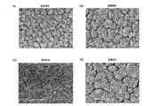
- FIG. 1B is an electron micrograph (SEM image) of the surface of the electromagnetic wave transmitting laminated member 1 according to the embodiment of the present invention.
- 2 (a) and 2 (b) show an example of an electron micrograph (TEM image) of a cross section of an electromagnetic wave transmitting laminated member according to an embodiment of the present invention.
- FIG. 3 is a diagram for explaining a method of measuring the thickness of the metal layer of the electromagnetic wave transmitting laminated member according to the embodiment of the present invention.
- 4 (a) to 4 (d) show electron micrographs (TEM images) of cross sections of the laminated members of Examples 4 to 7, respectively.
- 5 (a) and 5 (b) show electron micrographs (TEM images) of cross sections of the laminated members of Comparative Examples 1 and 3.
- the electromagnetic wave transmissive laminated member according to the embodiment of the present invention includes a substrate, an indium oxide-containing layer formed on the substrate, and a metal layer formed on the indium oxide-containing layer, and the metal layer is at least a part.
- the oxygen atom ratio (O / (In + M) ratio) to the total of is 1.15 or less.
- FIG. 1A shows a schematic cross-sectional view of the electromagnetic wave transmitting laminated member 1 according to the embodiment of the present invention
- FIG. 1B shows the electromagnetic wave transmitting laminated member 1 according to the embodiment of the present invention.
- An example of an electron micrograph (SEM image) of the surface is shown.
- the image size in the electron micrograph is 1.2 ⁇ m ⁇ 0.9 ⁇ m.
- the electromagnetic wave transmitting laminated member 1 includes a substrate 10, an indium oxide-containing layer 11 formed on the substrate 10, and a metal layer formed on the indium oxide-containing layer 11. Includes 12 and.
- the indium oxide-containing layer 11 is provided on the surface of the substrate 10.
- the indium oxide-containing layer 11 may be provided directly on the surface of the substrate 10, or may be indirectly provided via a protective film or the like provided on the surface of the substrate 10.
- the indium oxide-containing layer 11 is provided on the surface of the substrate 10 in a continuous state, in other words, without any gaps.
- the smoothness and corrosion resistance of the indium oxide-containing layer 11 and thus the electromagnetic wave transmitting laminated member 1 can be improved, and the indium oxide-containing layer 11 can be formed in the plane without variation. Is also easy.
- the metal layer 12 is laminated on the indium oxide-containing layer 11.
- the metal layer 12 includes a plurality of portions 12a. By being laminated on the indium oxide-containing layer 11, these portions 12a are separated from each other by a gap 12b at least in a discontinuous state, in other words, at least in a part. Since they are separated by the gap 12b, the sheet resistance of these portions 12a increases and the interaction with the radio waves decreases, so that the radio waves can be transmitted.
- Each of these portions 12a is an aggregate of sputtered particles formed by vapor deposition, sputtering, or the like of a metal.
- the sputtered particles form a thin film on a substrate such as the substrate 10
- the surface diffusivity of the particles on the substrate affects the shape of the thin film.
- the "discontinuous state” referred to in the present specification means a state in which they are separated from each other by a gap 12b, and as a result, they are electrically insulated from each other. By being electrically insulated, the sheet resistance is increased, and the desired electromagnetic wave transmission can be obtained.
- the discontinuous form is not particularly limited, and includes, for example, islands, cracks, and the like.
- the “island” means particles that are aggregates of sputtered particles, as shown in an electron micrograph (SEM image) of the surface of the metal layer of the electromagnetic wave transmitting laminated member in FIG. 1 (b). Means a structure in which the particles are laid out in a state where they are slightly separated from each other or partially in contact with each other.
- the crack structure is a structure in which a metal thin film is divided by cracks.
- the metal layer 12 having a crack structure can be formed, for example, by providing a metal thin film layer on an indium oxide-containing layer formed on a substrate and bending and stretching the metal thin film layer to cause cracks in the metal thin film layer.
- the metal layer 12 having a crack structure can be easily formed by providing a brittle layer made of a material having poor elasticity, that is, easily forming cracks by stretching, between the indium oxide-containing layer and the metal thin film layer. can.
- the mode in which the metal layer 12 is discontinuous is not particularly limited, but from the viewpoint of productivity, it is preferably "island-shaped".
- Electromagnetic wave transmission of the laminated member 1 can be evaluated by, for example, the amount of radio wave transmission attenuation.
- the amount of radio wave transmission attenuation can be measured, for example, by the method described later in the examples.
- the electromagnetic wave transmission laminated member having excellent electromagnetic wave transmission in the wave band is also excellent in electromagnetic wave transmission in the frequency band of the millimeter wave radar.
- the amount of radio wave transmission attenuation in the microwave band (28 GHz) is preferably less than 10 [ ⁇ dB], more preferably less than 5 [ ⁇ dB], and even more preferably less than 2 [ ⁇ dB]. .. If the amount of radio wave transmission attenuation in the microwave band (28 GHz) is 10 [ ⁇ dB] or more, there is a problem that 90% or more of the radio waves are blocked.
- the sheet resistance of the electromagnetic wave transmissive laminated member 1 also has a correlation with the electromagnetic wave transmissivity.
- the sheet resistance of the electromagnetic wave transmitting laminated member 1 is preferably 100 ⁇ / ⁇ or more.
- the amount of radio wave transmission attenuation in the microwave band (28 GHz) can be set to less than about 10 [ ⁇ dB].
- the sheet resistance of the electromagnetic wave transmitting laminated member 1 is more preferably 200 ⁇ / ⁇ or more, further preferably 600 ⁇ / ⁇ or more, and particularly preferably 1000 ⁇ / ⁇ or more.
- the sheet resistance of the electromagnetic wave transmitting laminated member 1 can be measured by the eddy current measuring method according to JIS-Z2316-1: 2014.
- the amount of radio wave transmission attenuation and sheet resistance of the electromagnetic wave transmission laminated member 1 are affected by the material and thickness of the indium oxide-containing layer 11 and the metal layer 12.
- Examples of the substrate 10 include resins, glasses, ceramics, and the like from the viewpoint of electromagnetic wave transmission.
- the substrate 10 may be any of a substrate film, a resin molded substrate, a glass substrate, or an article to which metallic luster should be imparted.
- examples of the base film include polyethylene terephthalate (PET), polyethylene naphthalate (PEN), polybutylene terephthalate, polyamide, polyvinyl chloride, polycarbonate (PC), cycloolefin polymer (COP), and polystyrene.
- PET polyethylene terephthalate
- PEN polyethylene naphthalate
- PC polycarbonate
- COP cycloolefin polymer
- polystyrene polystyrene
- Polypropylene (PP) polyethylene, polycycloolefin, polyurethane, acrylic (PMMA), ABS and other homopolymers and copolymers can be used.
- the layer 11 and the metal layer 12 can withstand high temperatures such as vapor deposition and sputtering.
- polyethylene terephthalate polyethylene naphthalate
- acrylic polycarbonate
- cycloolefin polymer ABS
- polypropylene polyurethane
- polyethylene terephthalate, cycloolefin polymer, polycarbonate, and acrylic are preferable because they have a good balance between heat resistance and cost.
- the base film may be a single-layer film or a laminated film. From the viewpoint of ease of processing and the like, the thickness is preferably, for example, 6 ⁇ m to 250 ⁇ m.
- the base film may be subjected to plasma treatment, easy adhesion treatment, or the like in order to strengthen the adhesive force with the indium oxide-containing layer 11 or the metal layer 12. Moreover, it is preferable that the base film does not contain particles.
- the base film is only an example of an object (base 10) on which the indium oxide-containing layer 11 can be formed.
- the substrate 10 includes a resin molded substrate, a glass substrate, and the article itself to which metallic luster should be imparted, in addition to the substrate film as described above.
- Examples of the resin molded base material and the articles to which the metallic luster should be imparted include vehicle structural parts, vehicle-mounted products, electronic device housings, home appliance housings, structural parts, mechanical parts, and various automobiles. Examples include parts for household appliances such as parts for electronic devices, furniture, kitchen utensils, medical equipment, parts for building materials, other structural parts, and exterior parts.
- the indium oxide-containing layer 11 is formed on the substrate 10.
- the indium oxide-containing layer 11 may be provided directly on the surface of the substrate 10, or may be indirectly provided via a protective film or the like provided on the surface of the substrate 10.
- the indium oxide-containing layer 11 is provided continuously on the surface of the substrate 10 to which metallic luster should be imparted, in other words, without any gaps.
- the smoothness and corrosion resistance of the indium oxide-containing layer 11, the metal layer 12, and the electromagnetic wave transmitting laminated member 1 can be improved. Further, it becomes easy to form the indium oxide-containing layer 11 in the plane without variation.
- the metal layer 12 Is easy to form in a discontinuous state.
- the surface diffusivity of the particles on the substrate affects the shape of the thin film, and the substrate. It is considered that the higher the temperature of the metal layer and the smaller the wettability of the metal layer with respect to the substrate, the easier it is to form a discontinuous structure. Then, it is considered that by providing the indium oxide-containing layer on the substrate, the surface diffusivity of the metal particles on the surface thereof is promoted, and the metal layer can be easily grown in a discontinuous state.
- the indium oxide-containing layer 11 has an indium atom and at least one metal of Sn and Zn when the surface thereof is measured by X-ray photoelectron spectroscopy.
- the oxygen atom ratio (O / (In + M) ratio) to the total with the atom M is 1.15 or less.
- the thickness of the metal layer 12 formed on the indium oxide-containing layer 11 can be controlled in a wide range.
- M in the oxygen atom ratio refers to both Sn and Zn metal atoms contained therein. It shall mean the total amount.
- the indium oxide-containing layer 11 has the oxygen atom ratio of 1.15 or less, preferably 1.13 or less.
- the lower limit of the oxygen atom ratio is not particularly limited, but is, for example, 0.5 or more.
- the thickness of the metal layer 12 can be controlled over a wide range because the oxygen atom ratio in the indium oxide-containing layer 11 is 1.15 or less, but it is presumed as follows.
- the ease of forming the discontinuous structure is related to the surface diffusion on the applied member (indium oxide-containing layer 11 in the present invention) to which the metal layer 12 is applied. It is considered that the higher the temperature of the applied member and the smaller the wettability of the metal layer 12 with respect to the applied member, the easier it is to form a discontinuous structure.
- the oxygen concentration of the indium oxide-containing layer 11, which is the member to which the metal layer 12 is applied low below a certain value, the wettability can be further reduced, and a discontinuous structure is formed. Is promoted. Therefore, it is presumed that the thickness of the discontinuous structure can be controlled in a wide range.
- the indium oxide-containing layer 11 can contain a metal-containing substance such as indium oxide (In 2 O 3 ), indium tin oxide (ITO), and indium zinc oxide (IZO).
- a metal-containing substance such as indium oxide (In 2 O 3 ), indium tin oxide (ITO), and indium zinc oxide (IZO).
- the thickness of the indium oxide-containing layer 11 is usually preferably 1000 nm or less, more preferably 50 nm or less, still more preferably 20 nm or less, from the viewpoint of sheet resistance, electromagnetic wave transmission, and productivity.
- the thickness of the indium oxide-containing layer 11 is preferably 1 nm or more, more preferably 2 nm or more, and further preferably 5 nm or more. preferable.
- the metal layer 12 is formed on the indium oxide-containing layer 11.
- the metal layer 12 is a layer having a metallic appearance, and is preferably a layer having a metallic luster.
- the material forming the metal layer 12 is not particularly limited, and may contain a metal or a resin, or may contain a metal and a resin.
- the thickness of the metal layer 12 can be controlled over a wide range by setting the oxygen atom ratio in the indium oxide-containing layer 11 within a specific range. Therefore, the thickness of the metal layer 12 can be set in a wide range of, for example, 10 nm to 200 nm, the yield is improved, and stable production is possible.
- the thickness of the metal layer 12 is usually preferably 10 nm or more from the viewpoint of exhibiting sufficient metallic luster, while it is usually preferably 200 nm or less from the viewpoint of sheet resistance and electromagnetic wave transmission.
- the thickness of the metal layer 12 is more preferably 10 nm to 100 nm, further preferably 10 nm to 70 nm. This thickness is also suitable for forming a uniform film with good productivity.
- the final product, the resin molded product looks good.
- the metal layer 12 is formed on the indium oxide-containing layer 11 and contains a plurality of portions that are discontinuous with each other at least in part.
- the metal layer 12 has a relatively low melting point as well as being able to exhibit sufficient brilliance. This is because the metal layer 12 is preferably formed by thin film growth using sputtering.
- a metal having a melting point of about 1100 ° C. or lower is suitable as the metal layer 12, and for example, aluminum (Al), zinc (Zn), lead (Pb), copper (Cu), and silver (Ag). ), And any of an alloy containing the metal as a main component is preferably contained.
- the metal layer 12 contains aluminum or an aluminum alloy because of the brilliance, stability, price, etc. of the substance.
- the aluminum content in the metal layer 12 is preferably 50% by mass or more.
- the equivalent circle diameter of the portion 12a of the metal layer 12 is not particularly limited, but is usually 10 to 1000 nm.
- the average particle size of the plurality of portions 12a means the average value of the equivalent circle diameters of the plurality of portions 12a.
- the circle-equivalent diameter of the portion 12a is the diameter of a perfect circle corresponding to the area of the portion 12a.
- the distance between the parts 12a is not particularly limited, but is usually 10 to 1000 nm.
- the ratio of the thickness of the metal layer 12 to the thickness of the indium oxide-containing layer 11 is preferably in the range of 0.02 to 100, and is preferably 0.1 to 100. Is more preferable, and the range of 0.3 to 35 is even more preferable. Within the above range, a uniform film can be formed with good productivity. In addition, the final product, the resin molded product, looks good. ⁇ 5. Other layers>
- electromagnetic wave transmitting laminated member 1 may be provided with other layers depending on the application, in addition to the above-mentioned indium oxide-containing layer 11 and the metal layer 12.
- Other layers include an optical adjustment layer (color adjustment layer) such as a high-refractive material for adjusting the appearance such as color, and a protective layer (scratch resistance layer) for improving durability such as scratch resistance. , Barrier layer (corrosion resistant layer), easy-adhesion layer, hard coat layer, antireflection layer, light extraction layer, anti-glare layer and the like.
- the method for producing the electromagnetic wave transmissive laminated member according to the present embodiment includes an indium oxide-containing layer forming step of forming an indium oxide-containing layer on a substrate and a metal layer forming step of forming a metal layer on the indium oxide-containing layer.
- an indium oxide-containing layer is formed on a substrate by reactive sputtering while supplying an inert gas and an oxygen gas using a metal target containing indium as a main component. It is a feature.
- Indium oxide-containing layer forming step In this step, the indium oxide-containing layer 11 is formed on the substrate 10.
- the formed indium oxide-containing layer 11 has an oxygen atom ratio (O / (In + M)) with respect to the sum of the indium atom and at least one metal atom M of Sn and Zn when the surface thereof is measured by X-ray photoelectron spectroscopy. ) Ratio) is 1.15 or less.
- an indium oxide-containing layer is formed on the substrate by reactive sputtering while supplying an inert gas and an oxygen gas using a metal target containing indium as a main component.
- the oxygen atom ratio in the above-mentioned predetermined range can be realized by appropriately setting the oxygen gas partial pressure ratio and performing reactive sputtering while adjusting the amount of oxygen to be supplied.
- indium oxides such as indium oxide (In 2 O 3 ), indium tin oxide (ITO), and indium zinc oxide (IZO) are often used as targets for forming the indium oxide-containing layer.
- rice field In such a method, since the target originally contains oxygen, it is difficult to adjust the oxygen concentration of the formed indium oxide-containing layer.
- an indium oxide-containing layer is formed by reactive sputtering while supplying an inert gas and an oxygen gas using a metal target containing indium containing no oxygen as a main component.
- the oxygen concentration in the indium oxide-containing layer can be suppressed to a low level, and as a result, the thickness of the metal layer 12 can be controlled over a wide range.
- the reactive sputtering for example, a pressure 0.1 to 1.0 Pa, direct current (DC) or radio frequency (RF) magnetron sputtering method can be applied.
- DC direct current
- RF radio frequency
- the metal target containing indium as a main component is not particularly limited as long as it does not contain oxygen.
- indium tin (Sn), zinc (Zn) and the like may be contained.
- the "main component” means the component having the highest content ratio (mass basis) among all the components in the metal target.
- Indium is preferably contained in a metal target in an amount of 70% by mass or more, more preferably 90% by mass or more.
- tin (Sn) When tin (Sn) is contained, it is preferably contained in the metal target in an amount of, for example, 2.5 to 30% by mass, more preferably 3 to 10% by mass.
- zinc (Zn) When zinc (Zn) is contained, it is preferably contained in the metal target in an amount of, for example, 2 to 20% by mass, more preferably 5 to 15% by mass.
- Argon and nitrogen are usually used as the inert gas.
- the oxygen gas partial pressure ratio (O 2 / Ar + O 2 ) can be appropriately set so that the oxygen atom ratio in the present invention can be obtained.
- the oxygen gas partial pressure ratio is usually preferably 28% or less, more preferably 27% or less, and further preferably 26% or less.
- the oxygen gas partial pressure ratio is, for example, 10% or more and 26% or less.
- the indium oxide-containing layer formed as described above preferably contains an indium oxide such as indium oxide (In 2 O 3 ), indium tin oxide (ITO), and indium zinc oxide (IZO).
- an indium oxide such as indium oxide (In 2 O 3 ), indium tin oxide (ITO), and indium zinc oxide (IZO).
- the metal layer 12 is laminated on the indium oxide-containing layer 11.
- sputtering can be used. It is preferable that the indium oxide-containing layer 11 and the metal layer 12 are in direct contact with each other without interposing another layer. However, if the mechanism of surface diffusion of the metal layer 12 on the indium oxide-containing layer 11 described above is ensured, another layer can be interposed.
- electromagnetic wave transmissive laminated members Since the electromagnetic wave transmissive laminated member of the present embodiment has electromagnetic wave transmissivity, it is preferable to use it for a device or an article for transmitting and receiving electromagnetic waves, its parts, and the like.
- applications for household goods such as structural parts for vehicles, vehicle-mounted products, housings for electronic devices, housings for home appliances, structural parts, mechanical parts, various automobile parts, electronic device parts, furniture, kitchen supplies, etc. , Medical equipment, building material parts, other structural parts, exterior parts, etc.
- ECU box electrical components, engine peripheral parts, drive system / gear peripheral parts, intake / exhaust system parts, cooling system parts, and the like.
- home appliances such as refrigerators, washing machines, vacuum cleaners, microwave ovens, air conditioners, lighting devices, electric water heaters, TVs, watches, ventilation fans, projectors, speakers, personal computers, and portable devices.
- home appliances such as refrigerators, washing machines, vacuum cleaners, microwave ovens, air conditioners, lighting devices, electric water heaters, TVs, watches, ventilation fans, projectors, speakers, personal computers, and portable devices.
- Examples thereof include telephones, smartphones, digital cameras, tablet PCs, portable music players, portable game machines, chargers, and electronic information devices such as batteries.
- Radio wave transmission attenuation The radio wave transmission attenuation at 28 GHz was measured and evaluated using a free space method measuring device LAF-26.5A manufactured by Keycom Co., Ltd. and a spectrum analyzer MS4644BCXA siginal Analyzer NA9000A manufactured by Anritsu and Azirent. (Evaluation of electromagnetic wave transmission) Less than 2 [-dB]: ⁇ 2 [-dB] or more and less than 5 [-dB]: ⁇ 5 [-dB] or more and less than 10 [-dB]: ⁇ 10 [-dB] or more: ⁇
- a square region having a side of 5 cm as shown in FIG. 3 A total of 5 points "a” to "e” obtained by appropriately extracting 3 and dividing the center lines A and B of the vertical side and the horizontal side of the square region 3 into 4 equal parts are used as measurement points. Selected.
- a viewing angle region including approximately five portions 12a was extracted. Approximately 5 parts 12a at each of these 5 measurement points, that is, the individual thicknesses of 25 (5 x 5) parts 12a are obtained, and the average value thereof is defined as the "maximum thickness". And said.
- ⁇ Thickness of indium oxide-containing layer> The thickness of the indium oxide-containing layer was measured using the same method as the metal layer. That is, the thickness of the indium oxide-containing layer at the portion corresponding to the 25 portions 12a selected at the time of measuring the thickness of the metal layer was obtained, and the average value thereof was obtained and used as the thickness of the indium oxide-containing layer.
- Example 1 As the base film, a PET film (thickness 50 ⁇ m) on which a hard coat layer containing no particles was formed was used. First, using an In—Sn alloy target (Sn ratio 5% by mass), the oxygen gas partial pressure ratio (O 2 / (Ar + O 2 )) is set to 26% by DC pulse sputtering (150 kHz), and hard coating is performed. ITO was formed on the layer. The temperature of the base film when forming the ITO layer was set to 130 ° C. Next, an aluminum (Al) layer was formed on the ITO layer by using AC sputtering (AC: 40 kHz) to obtain an electromagnetic wave transmitting laminated member shown in Table 1. The obtained aluminum layer was a discontinuous layer. The temperature of the base film when forming the Al layer was set to 130 ° C.
- AC sputtering AC: 40 kHz
- Example 2 to 7 The laminated members of Examples 2 to 7 shown in Table 1 were obtained in the same manner as in Example 1 except that the time for forming the ITO layer and the time for forming the aluminum (Al) layer were changed. Electron micrographs (TEM images) of cross sections of the laminated members of Examples 4 to 7 are shown in FIGS. 4 (a) to 4 (d), respectively.
- Comparative Example 1 The laminated member of Comparative Example 1 shown in Table 1 was obtained in the same manner as in Example 5 except that the oxygen gas partial pressure ratio (O 2 / (Ar + O 2 )) at the time of ITO film formation in Example 5 was changed to 29%. rice field. An electron micrograph (TEM image) of a cross section of the laminated member of Comparative Example 1 is shown in FIG. 5 (a).
- Comparative Examples 2 to 3 The laminated members of Comparative Examples 2 and 3 shown in Table 1 were obtained in the same manner as in Comparative Example 1 except that the time for forming the ITO layer and the time for forming the aluminum (Al) layer were changed.
- FIG. 5 (b) An electron micrograph (TEM image) of a cross section of the laminated member of Comparative Example 3 is shown in FIG. 5 (b).
- Table 1 shows the same as in Comparative Example 1 except that the target material was an ITO target (Sn ratio 10% by mass) and the oxygen gas partial pressure ratio (O 2 / (Ar + O 2)) at the time of ITO film formation was changed to 0%.
- the laminated member of Comparative Example 4 shown was obtained.
- the evaluation results are shown in Table 1 below.
- the laminated members of Comparative Examples 1 to 4 had extremely low sheet resistance and high radio wave transmission attenuation, and were inferior in electromagnetic wave transmission compared to Examples.
- TEM images electron micrographs of the cross sections of the laminated members of Comparative Examples 1 and 3 shown in FIGS. 5 (a) and 5 (b)
- this is due to the large number of island-shaped metal layer portions. It is probable that they were formed by overlapping.
- metals other than aluminum (Al) particularly used in the above examples metals having a relatively low melting point such as zinc (Zn), lead (Pb), copper (Cu), and silver (Ag) are used. It is considered that a discontinuous structure can be formed by the same method.
- the electromagnetic wave transmissive laminated member according to the present invention can be used for devices, articles, and parts thereof that transmit and receive electromagnetic waves.
- applications for household goods such as structural parts for vehicles, vehicle-mounted products, housings for electronic devices, housings for home appliances, structural parts, mechanical parts, various automobile parts, electronic device parts, furniture, kitchen supplies, etc. It can also be used for various applications that require both design and electromagnetic wave transmission, such as medical equipment, building material parts, other structural parts and exterior parts.
- Electromagnetic wave transmissive laminated member 10 Base 11 Indium oxide-containing layer 12 Metal layer 12a Part 12b Gap
Abstract
基体と、前記基体上に形成された酸化インジウム含有層と、前記酸化インジウム含有層上に形成された金属層と、を備え、前記金属層は少なくとも一部において互いに不連続の状態にある複数の部分を含んでおり、前記酸化インジウム含有層の表面をX線光電子分光法により測定したときの、インジウム原子と、Sn及びZnの少なくとも1種の金属原子との合計に対する酸素原子比率(O/(In+M)比)が1.15以下である、電磁波透過性積層部材。
Description
本発明は、電磁波透過性積層部材、及びその製造方法に関する。
従来、電磁波透過性及び金属光沢を有する部材が、その金属光沢に由来する外観の高級感と、電磁波透過性とを兼ね備えることから、電磁波を送受信する装置に好適に用いられている。
金属光沢調の部材に金属を使用した場合には、電磁波の送受信が実質的に不可能または妨害されてしまう。したがって、電磁波の送受信を妨げることなく、意匠性を損なわせないために、金属光沢と電磁波透過性の双方を兼ね備えた電磁波透過性積層部材が必要とされている。
このような電磁波透過性積層部材は、電磁波を送受信する装置として、通信を必要とする様々な機器、例えば、スマートキーを設けた自動車のドアハンドル、車載通信機器、携帯電話、パソコン等の電子機器等への応用が期待されている。更に、近年では、IoT技術の発達に伴い、従来は通信等行われることがなかった、冷蔵庫等の家電製品、生活機器等、幅広い分野での応用も期待されている。
電磁波透過性積層部材に関して、特許文献1には、基体の面に設けた酸化インジウム含有層と、前記酸化インジウム含有層に積層された金属層と、を備え、前記金属層は、少なくとも一部において互いに不連続の状態にある複数の部分を含むことを特徴とする電磁波透過性金属光沢部材が記載されている。
従来技術の電磁波透過性積層部材における金属層は、その形成方法や基体の種類にもよるが、50nm程度の厚みまでしか形成することができなかった。それ以上の厚みになると島状に形成された金属同士が重なり合ってしまい、抵抗値が急激に低下するため、電磁波透過性が著しく損なわれてしまう。そのため、金属層の厚みに関し、数ナノオーダーでの膜厚管理が必要となり、安定した生産が難しく、歩留まり低下を引き起こすという問題が生じていた。
本発明は、従来技術における上記問題を解決するためになされたものであり、優れた電磁波透過性を有し、かつ、金属層の厚みを広範囲に制御可能な、電磁波透過性積層部材を提供することを目的とする。
本発明者等は、上記課題を解決するために鋭意検討を重ねた結果、酸化インジウム含有層における酸素濃度を特定範囲とすることにより、上記課題を解決できることを見出し、本発明を完成するに至った。
すなわち、本発明は以下のとおりである。
[1]
基体と、前記基体上に形成された酸化インジウム含有層と、前記酸化インジウム含有層上に形成された金属層と、を備え、
前記金属層は少なくとも一部において互いに不連続の状態にある複数の部分を含んでおり、
前記酸化インジウム含有層の表面をX線光電子分光法により測定したときの、インジウム原子と、Sn及びZnの少なくとも1種の金属原子Mとの合計に対する酸素原子比率(O/(In+M)比)が1.15以下である、
電磁波透過性積層部材。
[2]
前記酸化インジウム含有層が連続状態で設けられている、前記[1]に記載の電磁波透過性積層部材。
[3]
前記酸化インジウム含有層が、酸化インジウム(In2O3)、インジウム錫酸化物(ITO)、又はインジウム亜鉛酸化物(IZO)のいずれかを含む、前記[1]または[2]に記載の電磁波透過性積層部材。
[4]
前記金属層が、アルミニウム又はアルミニウム合金を含有する層である前記[1]~[3]のいずれか1に記載の電磁波透過性積層部材。
[5]
前記酸化インジウム含有層の厚さは、1nm~1000nmである、前記[1]~[4]のいずれか1に記載の電磁波透過性積層部材。
[6]
前記金属層の厚さは、10nm~200nmである、前記[1]~[5]のいずれか1に記載の電磁波透過性積層部材。
[7]
前記金属層の厚さと前記酸化インジウム含有層の厚さとの比(前記金属層の厚さ/前記酸化インジウム含有層の厚さ)は、0.02~100である、前記[1]~[6]のいずれか1に記載の電磁波透過性積層部材。
[8]
シート抵抗が、100Ω/□以上である、前記[1]~[7]のいずれか1に記載の電磁波透過性積層部材。
[9]
前記複数の部分が島状に形成されている、前記[1]~[8]のいずれか1に記載の電磁波透過性積層部材。
[10]
前記基体が、基材フィルム、樹脂成型物基材、ガラス基材、又は金属光沢を付与すべき物品のいずれかである、前記[1]~[9]のいずれか1に記載の電磁波透過性積層部材。
[11]
基体上に酸化インジウム含有層を形成する酸化インジウム含有層形成工程と、
前記酸化インジウム含有層の上に金属層を形成する金属層形成工程と、を含み、
前記酸化インジウム含有層形成工程は、インジウムを主成分として含む金属ターゲットを用い、不活性ガスおよび酸素ガスを供給しながら、反応性スパッタリングにより前記基体上に酸化インジウム含有層を形成する、前記[1]~[10]のいずれか1に記載の電磁波透過性積層部材を製造する方法。
本発明によれば、電磁波透過性に優れ、かつ、金属層の厚みを広範囲に制御可能な、電磁波透過性積層部材を提供することができる。
以下、添付図面を参照しつつ、本発明を詳細に説明するが、本発明は以下の実施形態に限定されるものではなく、本発明の要旨を逸脱しない範囲において、任意に変形して実施できる。また、数値範囲を示す「~」とは、その前後に記載された数値を下限値及び上限値として含む意味で使用される。
<1.基本構成>
本発明の実施形態にかかる電磁波透過性積層部材は、基体と、基体上に形成された酸化インジウム含有層と、酸化インジウム含有層上に形成された金属層とを備え、金属層は少なくとも一部において互いに不連続の状態にある複数の部分を含んでおり、酸化インジウム含有層の表面をX線光電子分光法により測定したときの、インジウム原子と、Sn及びZnの少なくとも1種の金属原子Mとの合計に対する酸素原子比率(O/(In+M)比)が1.15以下であることを特徴とする。
本発明の実施形態にかかる電磁波透過性積層部材は、基体と、基体上に形成された酸化インジウム含有層と、酸化インジウム含有層上に形成された金属層とを備え、金属層は少なくとも一部において互いに不連続の状態にある複数の部分を含んでおり、酸化インジウム含有層の表面をX線光電子分光法により測定したときの、インジウム原子と、Sn及びZnの少なくとも1種の金属原子Mとの合計に対する酸素原子比率(O/(In+M)比)が1.15以下であることを特徴とする。
図1(a)に、本発明の一実施形態における電磁波透過性積層部材1の概略断面図を示し、また、図1(b)に、本発明の一実施形態における電磁波透過性積層部材1の表面の電子顕微鏡写真(SEM画像)の一例を示す。なお、電子顕微鏡写真における画像サイズは1.2μm×0.9μmである。
図1(a)に示すように、電磁波透過性積層部材1は、基体10と、基体10の上に形成された酸化インジウム含有層11と、酸化インジウム含有層11の上に形成された金属層12とを含む。
酸化インジウム含有層11は、基体10の面に設けられている。酸化インジウム含有層11は、基体10の面に直接設けられていてもよいし、基体10の面に設けた保護膜等を介して間接的に設けられてもよい。
酸化インジウム含有層11は、基体10の面に連続状態で、言い換えれば、隙間なく、設けるのが好ましい。連続状態で設けることにより、酸化インジウム含有層11、ひいては、電磁波透過性積層部材1の平滑性や耐食性を向上させることができ、また、酸化インジウム含有層11を面内にばらつきなく成膜することも容易となる。
金属層12は酸化インジウム含有層11に積層される。金属層12は複数の部分12aを含む。酸化インジウム含有層11に積層されることにより、これらの部分12aは、少なくとも一部において互いに不連続の状態、言い換えれば、少なくとも一部において隙間12bによって隔てられる。隙間12bによって隔てられるため、これらの部分12aのシート抵抗は大きくなり、電波との相互作用が低下するため、電波を透過させることができる。
これらの各部分12aは、金属を蒸着、スパッタ等することによって形成されたスパッタ粒子の集合体である。スパッタ粒子が基体10等の基体上で薄膜を形成する際には、基体上での粒子の表面拡散性が薄膜の形状に影響を及ぼす。
なお、本明細書でいう「不連続の状態」とは、隙間12bによって互いに隔てられており、この結果、互いに電気的に絶縁されている状態を意味する。電気的に絶縁されることにより、シート抵抗が大きくなり、所望とする電磁波透過性が得られることになる。不連続の形態は、特に限定されるものではなく、例えば、島状、クラック等が含まれる。
ここで「島状」とは、図1(b)の電磁波透過性積層部材の金属層の表面の電子顕微鏡写真(SEM画像)に示されているように、スパッタ粒子の集合体である粒子同士が各々独立しており、それらの粒子が、互いに僅かに離間し又は一部接触した状態で敷き詰められてなる構造を意味する。
また、クラック構造とは、金属薄膜がクラックにより分断された構造である。クラック構造の金属層12は、例えば基体上に形成した酸化インジウム含有層上に、金属薄膜層を設け、屈曲延伸して金属薄膜層にクラックを生じさせることにより形成することができる。この際、酸化インジウム含有層と金属薄膜層の間に伸縮性に乏しい、即ち延伸によりクラックを生成しやすい素材からなる脆性層を設けることにより、容易にクラック構造の金属層12を形成することができる。
上述のとおり金属層12が不連続となる態様は特に限定されないが、生産性の観点からは「島状」とすることが好ましい。
電磁波透過性積層部材1の電磁波透過性は、例えば電波透過減衰量により評価することができる。電波透過減衰量は、例えば、実施例で後述する方法で測定できる。
なお、マイクロ波帯域(28GHz)における電波透過減衰量とミリ波レーダーの周波数帯域(76~80GHz)における電波透過減衰量との間には相関性があり、比較的近い値を示すことから、マイクロ波帯域における電磁波透過性に優れる電磁波透過性積層部材は、ミリ波レーダーの周波数帯域における電磁波透過性にも優れる。
マイクロ波帯域(28GHz)における電波透過減衰量は、10[-dB]未満であることが好ましく、5[-dB]未満であるのがより好ましく、2[-dB]未満であることが更に好ましい。マイクロ波帯域(28GHz)における電波透過減衰量が10[-dB]以上であると、90%以上の電波が遮断されるという問題がある。
電磁波透過性積層部材1のシート抵抗も電磁波透過性と相関を有する。
電磁波透過性積層部材1のシート抵抗は100Ω/□以上であることが好ましい。この場合、マイクロ波帯域(28GHz)における電波透過減衰量は、10[-dB]未満程度とすることが可能である。
電磁波透過性積層部材1のシート抵抗は200Ω/□以上であることが更に好ましく、600Ω/□以上であることがより更に好ましく、1000Ω/□以上であることが特に好ましい。
電磁波透過性積層部材1のシート抵抗は、JIS-Z2316-1:2014に従って渦電流測定法により測定することができる。
電磁波透過性積層部材1の電波透過減衰量及びシート抵抗は、酸化インジウム含有層11や金属層12の材質や厚さ等により影響を受ける。
<2.基体>
基体10としては、電磁波透過性の観点から、例えば、樹脂、ガラス、セラミックス等が挙げられる。
基体10としては、電磁波透過性の観点から、例えば、樹脂、ガラス、セラミックス等が挙げられる。
基体10は、基材フィルム、樹脂成型物基材、ガラス基材、又は金属光沢を付与すべき物品のいずれかであってもよい。
より具体的には、基材フィルムとしては、例えば、ポリエチレンテレフタレート(PET)、ポリエチレンナフタレート(PEN)、ポリブチレンテレフタレート、ポリアミド、ポリ塩化ビニル、ポリカーボネート(PC)、シクロオレフィンポリマー(COP)、ポリスチレン、ポリプロピレン(PP)、ポリエチレン、ポリシクロオレフィン、ポリウレタン、アクリル(PMMA)、ABS等の単独重合体や共重合体からなる透明フィルムを用いることができる。
これらの部材によれば、光輝性や電磁波透過性に影響を与えることがない。但し、酸化インジウム含有層11や金属層12を後に形成する観点から、蒸着やスパッタ等の高温に耐え得るものであることが好ましい。
そのため、上記材料の中でも、例えば、ポリエチレンテレフタレート、ポリエチレンナフタレート、アクリル、ポリカーボネート、シクロオレフィンポリマー、ABS、ポリプロピレン、及びポリウレタンが好ましい。
なかでも、耐熱性とコストとのバランスがよいことから、ポリエチレンテレフタレート、シクロオレフィンポリマー、ポリカーボネート、及びアクリルが好ましい。
基材フィルムは、単層フィルムでもよいし積層フィルムでもよい。加工のし易さ等から、厚さは、例えば、6μm~250μmが好ましい。
基材フィルムは、酸化インジウム含有層11や金属層12との付着力を強くするために、プラズマ処理や易接着処理などが施されてもよい。また、基材フィルムは、粒子を含有しないものであることが好ましい。
ここで、基材フィルムは、その表面上に酸化インジウム含有層11を形成することができる対象(基体10)の一例にすぎない点に注意すべきである。
基体10には、上記のとおり基材フィルムの他、樹脂成型物基材、ガラス基材、金属光沢を付与すべき物品それ自体も含まれる。
樹脂成型物基材、及び金属光沢を付与すべき物品としては、例えば、車両用構造部品、車両搭載用品、電子機器の筐体、家電機器の筐体、構造用部品、機械部品、種々の自動車用部品、電子機器用部品、家具、台所用品等の家財向け用途、医療機器、建築資材の部品、その他の構造用部品、及び外装用部品等が挙げられる。
<3.酸化インジウム含有層>
酸化インジウム含有層11は、基体10の上に形成される。酸化インジウム含有層11は、基体10の面に直接設けられていてもよいし、基体10の面に設けられた保護膜等を介して間接的に設けられてもよい。
酸化インジウム含有層11は、基体10の上に形成される。酸化インジウム含有層11は、基体10の面に直接設けられていてもよいし、基体10の面に設けられた保護膜等を介して間接的に設けられてもよい。
酸化インジウム含有層11は、金属光沢を付与すべき基体10の面に連続状態で、言い換えれば、隙間なく、設けるのが好ましい。酸化インジウム含有層11が連続状態で設けられることにより、酸化インジウム含有層11、ひいては、金属層12や電磁波透過性積層部材1の平滑性や耐食性を向上させることができる。また、酸化インジウム含有層11を面内にばらつきなく成膜することも容易となる。
このように、基体10上に酸化インジウム含有層11を備えること、すなわち、基体10の上に酸化インジウム含有層11を形成し、その上に後述する金属層12を積層することで、金属層12を不連続の状態で形成しやすくなる。
上記メカニズムの詳細は必ずしも明らかではないが、金属の蒸着やスパッタによるスパッタ粒子が基体上で薄膜を形成する際には、基体上での粒子の表面拡散性が薄膜の形状に影響を及ぼし、基体の温度が高く、基体に対する金属層の濡れ性が小さい方が不連続構造を形成しやすいと考えられる。そして、基体上に酸化インジウム含有層を設けることにより、その表面上の金属粒子の表面拡散性が促進されて、金属層を不連続の状態で成長させやすくなると考えられる。
また、本発明の実施形態にかかる電磁波透過性積層部材において、酸化インジウム含有層11は、その表面をX線光電子分光法により測定したときの、インジウム原子と、Sn及びZnの少なくとも1種の金属原子Mとの合計に対する酸素原子比率(O/(In+M)比)が1.15以下であることを特徴とする。
酸化インジウム含有層11における上記酸素原子比率が1.15以下であることによって、酸化インジウム含有層11上に形成される金属層12の厚みを広範囲に制御することが可能となる。
なお、上記酸素原子比率(O/(In+M)比)におけるMとは、酸化インジウム含有層がSn及びZnの両方の金属原子を含有する場合には、含有するSn及びZnの両方の金属原子を合計した量を意味するものとする。
酸化インジウム含有層11は、上記酸素原子比率は1.15以下であり、好ましくは1.13以下である。また、上記酸素原子比率の下限値は特に限定されないが、例えば0.5以上である。
酸化インジウム含有層11における上記酸素原子比率が1.15以下であることにより、金属層12の厚みを広範囲に制御できる理由については明らかではないが、以下のように推測される。
すなわち、金属層12の形成プロセスにおいて、不連続構造の形成しやすさは、金属層12が付与される被付与部材(本発明では、酸化インジウム含有層11)上での表面拡散と関連性があり、被付与部材の温度が高く、被付与部材に対する金属層12の濡れ性が小さい方が不連続構造を形成しやすいと考えられる。
本発明においては、金属層12が付与される被付与部材である酸化インジウム含有層11の酸素濃度を一定値以下に低く抑えることにより、濡れ性を更に小さくすることができ、不連続構造の形成が促進される。そのため、当該不連続構造の厚みを広範囲に制御可能であると推察される。
酸化インジウム含有層11は、酸化インジウム(In2O3)、インジウム錫酸化物(ITO)や、インジウム亜鉛酸化物(IZO)のような金属含有物を含むことができる。
酸化インジウム含有層11が上記金属含有物を含むことにより、基体の面に沿って連続状態の膜を形成することもできる。また、この場合には、酸化インジウム含有層11の上に積層される金属層12を、例えば、島状の不連続構造としやすくなる。更に、この場合には、金属層12に、錫(Sn)又はインジウム(In)だけでなく、通常は不連続構造になり難く本用途には適用が難しかったアルミニウム等の様々な金属を含めやすくなる。
酸化インジウム含有層11の厚さは、シート抵抗や電磁波透過性、生産性の観点から、通常1000nm以下が好ましく、50nm以下がより好ましく、20nm以下が更に好ましい。
一方、積層される金属層12を不連続状態とするには、酸化インジウム含有層11の厚さは1nm以上であることが好ましく、2nm以上であることがより好ましく、5nm以上であることが更に好ましい。
<4.金属層>
金属層12は酸化インジウム含有層11の上に形成される。金属層12は、金属調の外観を有する層であり、金属光沢を有する層であることが好ましい。金属層12を形成する材料に特に限定はなく、金属、又は樹脂を含んでいてもよく、金属及び樹脂を含んでいてもよい。
金属層12は酸化インジウム含有層11の上に形成される。金属層12は、金属調の外観を有する層であり、金属光沢を有する層であることが好ましい。金属層12を形成する材料に特に限定はなく、金属、又は樹脂を含んでいてもよく、金属及び樹脂を含んでいてもよい。
本発明の実施形態にかかる電磁波透過性積層部材においては、酸化インジウム含有層11における上記酸素原子比率が特定範囲であることにより、金属層12の厚みを広範囲に制御できる。したがって、金属層12の厚さは、例えば、10nm~200nmの広範囲に設定することができ、歩留まりが向上し、安定した生産が可能となる。
十分な金属光沢を発揮するという観点で、金属層12の厚さは、通常10nm以上が好ましく、一方、シート抵抗や電磁波透過性の観点から、通常200nm以下が好ましい。
例えば、金属層12の厚さは、10nm~100nmがより好ましく、10nm~70nmが更に好ましい。この厚さは、均一な膜を生産性良く形成するのにも適する。また、最終製品である樹脂成形品の見栄えも良い。
金属層12は酸化インジウム含有層11上に形成され、少なくとも一部において互いに不連続の状態にある複数の部分を含む。
金属層12が酸化インジウム含有層11上で連続状態である場合、十分な金属光沢が得られるものの、電波透過減衰量が非常に大きくなるため、電磁波透過性を確保することはできない。
金属層12は、十分な光輝性を発揮し得ることは勿論、融点が比較的低いものであることが好ましい。金属層12は、スパッタリングを用いた薄膜成長によって形成するのが好ましいためである。
このような理由から、金属層12としては、融点が約1100℃以下の金属が適しており、例えば、アルミニウム(Al)、亜鉛(Zn)、鉛(Pb)、銅(Cu)、銀(Ag)から選択された少なくとも一種の金属、及び該金属を主成分とする合金のいずれかを含むことが好ましい。
特に、物質の光輝性や安定性、価格等の理由から、金属層12はアルミニウム又はアルミニウム合金を含むことがより好ましい。
また、アルミニウム合金を用いる場合には、金属層12におけるアルミニウム含有量を50質量%以上とすることが好ましい。
金属層12の部分12aの円相当径は特に限定されないが、通常10~1000nmである。複数の部分12aの平均粒径とは、複数の部分12aの円相当径の平均値を意味する。
部分12aの円相当径とは、部分12aの面積に相当する真円の直径のことである。
また、各部分12a同士の距離は特に限定されないが、通常は10~1000nmである。
金属層12の厚さと酸化インジウム含有層11の厚さとの比(金属層12の厚さ/酸化インジウム含有層11の厚さ)は、0.02~100の範囲が好ましく、0.1~100の範囲がより好ましく、0.3~35の範囲が更に好ましい。上記範囲とすることにより、均一な膜を生産性良く形成することができる。また、最終製品である樹脂成形品の見栄えも良い。
<5.その他の層>
<5.その他の層>
また、本発明の実施形態にかかる電磁波透過性積層部材1は、上述の酸化インジウム含有層11、及び金属層12の他に、用途に応じてその他の層を備えてもよい。
その他の層としては色味等の外観を調整するための高屈折材料等の光学調整層(色味調整層)、耐擦傷性等の耐久性を向上させるための保護層(耐擦傷性層)、バリア層(耐腐食層)、易接着層、ハードコート層、反射防止層、光取出し層、及びアンチグレア層等が挙げられる。
<6.電磁波透過性積層部材の製造方法>
本実施形態に係る電磁波透過性積層部材の製造方法は、基体上に酸化インジウム含有層を形成する酸化インジウム含有層形成工程と、酸化インジウム含有層の上に金属層を形成する金属層形成工程と、を含み、酸化インジウム含有層形成工程は、インジウムを主成分として含む金属ターゲットを用い、不活性ガスおよび酸素ガスを供給しながら、反応性スパッタリングにより基体上に酸化インジウム含有層を形成することを特徴とする。以下各工程について詳細に説明する。
本実施形態に係る電磁波透過性積層部材の製造方法は、基体上に酸化インジウム含有層を形成する酸化インジウム含有層形成工程と、酸化インジウム含有層の上に金属層を形成する金属層形成工程と、を含み、酸化インジウム含有層形成工程は、インジウムを主成分として含む金属ターゲットを用い、不活性ガスおよび酸素ガスを供給しながら、反応性スパッタリングにより基体上に酸化インジウム含有層を形成することを特徴とする。以下各工程について詳細に説明する。
(1)酸化インジウム含有層形成工程
本工程では、基体10上に酸化インジウム含有層11を形成する。形成される酸化インジウム含有層11は、その表面をX線光電子分光法により測定したときの、インジウム原子と、Sn及びZnの少なくとも1種の金属原子Mの合計に対する酸素原子比率(O/(In+M)比)が1.15以下となる。
本工程では、基体10上に酸化インジウム含有層11を形成する。形成される酸化インジウム含有層11は、その表面をX線光電子分光法により測定したときの、インジウム原子と、Sn及びZnの少なくとも1種の金属原子Mの合計に対する酸素原子比率(O/(In+M)比)が1.15以下となる。
上記酸素比率を実現するべく、本工程においては、インジウムを主成分として含む金属ターゲットを用い、不活性ガスおよび酸素ガスを供給しながら、反応性スパッタリングにより基体上に酸化インジウム含有層を形成する。かかる方法であれば、酸素ガス分圧比を適宜設定し、供給する酸素の量を調整しながら、反応性スパッタリングを行うことにより、上記所定範囲の酸素原子比率を実現できる。
従来、酸化インジウム含有層の形成には、酸化インジウム(In2O3)、インジウム錫酸化物(ITO)、及びインジウム亜鉛酸化物(IZO)等のインジウムの酸化物をターゲットとして用いられることが多かった。かかる方法では、元々ターゲットに酸素が含まれているため、形成される酸化インジウム含有層の酸素濃度を調整することが困難であった。
一方、本発明では、酸素を含まないインジウムを主成分とする金属ターゲット等を用い、不活性ガスおよび酸素ガスを供給しながら、反応性スパッタリングにより酸化インジウム含有層を形成する。これにより、酸化インジウム含有層内の酸素濃度を低く抑えることができ、その結果、金属層12の厚みを広範囲に制御することができる。
反応性スパッタリングとしては、例えば、圧力0.1~1.0Pa、直流(DC)あるいは高周波(RF)マグネトロンスパッタリング法を適用することができる。
インジウムを主成分とする金属ターゲットとしては、酸素を含むものでなければ、特に制限されない。例えば、インジウムの他に、錫(Sn)及び亜鉛(Zn)等を含有してもよい。組成式としては、InXM1-X(0.7≦x≦1、M=Sn及びZnからなる少なくとも1種の金属元素)と表すことができる。ここで「主成分」とは、金属ターゲット中の全成分の中で最も含有割合(質量基準)が多い成分を意味する。
インジウムは、金属ターゲット中に70質量%以上含有するのが好ましく、90質量%以上含有するのがより好ましい。
錫(Sn)を含有する場合は、金属ターゲット中に、例えば2.5~30質量%含有するのが好ましく、3~10質量%含有するのがより好ましい。
亜鉛(Zn)を含有する場合は、金属ターゲット中に、例えば2~20質量%含有するのが好ましく、5~15質量%含有するのがより好ましい。
不活性ガスとしては、アルゴン、窒素が通常用いられる。
不活性ガスとしてアルゴンを用いた場合の、酸素ガス分圧比(O2/Ar+O2)は、本発明における酸素原子比率が得られるように適宜設定することができる。上記酸素ガス分圧比は通常28%以下であることが好ましく、27%以下であることがより好ましく、26%以下であることが更に好ましい。また、上記酸素ガス分圧比は、例えば、10%以上、26%以下である。
不活性ガスとしてアルゴンを用いた場合の、酸素ガス分圧比(O2/Ar+O2)は、本発明における酸素原子比率が得られるように適宜設定することができる。上記酸素ガス分圧比は通常28%以下であることが好ましく、27%以下であることがより好ましく、26%以下であることが更に好ましい。また、上記酸素ガス分圧比は、例えば、10%以上、26%以下である。
以上のように形成された酸化インジウム含有層は、酸化インジウム(In2O3)、インジウム錫酸化物(ITO)、及びインジウム亜鉛酸化物(IZO)等のインジウムの酸化物を含むことが好ましい。
(2)酸化インジウム含有層形成工程
次いで、酸化インジウム含有層11の上に、金属層12を積層する。この場合も、例えば、スパッタリングを用いることができる。なお、酸化インジウム含有層11と金属層12の間には、他の層を介在させずに直接接触させるのが好ましい。但し、上に説明した酸化インジウム含有層11上における金属層12の表面拡散のメカニズムが確保されるのであれば、他の層を介在させることもできる。
次いで、酸化インジウム含有層11の上に、金属層12を積層する。この場合も、例えば、スパッタリングを用いることができる。なお、酸化インジウム含有層11と金属層12の間には、他の層を介在させずに直接接触させるのが好ましい。但し、上に説明した酸化インジウム含有層11上における金属層12の表面拡散のメカニズムが確保されるのであれば、他の層を介在させることもできる。
<7.電磁波透過性積層部材の用途>
本実施形態の電磁波透過性積層部材は、電磁波透過性を有することから電磁波を送受信する装置や物品及びその部品等に使用することが好ましい。例えば、車両用構造部品、車両搭載用品、電子機器の筐体、家電機器の筐体、構造用部品、機械部品、種々の自動車用部品、電子機器用部品、家具、台所用品等の家財向け用途、医療機器、建築資材の部品、その他の構造用部品や外装用部品等が挙げられる。
本実施形態の電磁波透過性積層部材は、電磁波透過性を有することから電磁波を送受信する装置や物品及びその部品等に使用することが好ましい。例えば、車両用構造部品、車両搭載用品、電子機器の筐体、家電機器の筐体、構造用部品、機械部品、種々の自動車用部品、電子機器用部品、家具、台所用品等の家財向け用途、医療機器、建築資材の部品、その他の構造用部品や外装用部品等が挙げられる。
より具体的には、車両関係では、インスツルメントパネル、コンソールボックス、ドアノブ、ドアトリム、シフトレバー、ペダル類、グローブボックス、バンパー、ボンネット、フェンダー、トランク、ドア、ルーフ、ピラー、座席シート、ステアリングホイール、ECUボックス、電装部品、エンジン周辺部品、駆動系・ギア周辺部品、吸気・排気系部品、及び冷却系部品等が挙げられる。
電子機器及び家電機器として、より具体的には、冷蔵庫、洗濯機、掃除機、電子レンジ、エアコン、照明機器、電気湯沸かし器、テレビ、時計、換気扇、プロジェクター、スピーカー等の家電製品類、パソコン、携帯電話、スマートフォン、デジタルカメラ、タブレット型PC、携帯音楽プレーヤー、携帯ゲーム機、充電器、及び電池等電子情報機器等が挙げられる。
以下、実施例及び比較例を挙げて、本発明をより具体的に説明する。
電磁波透過性積層部材1に関して各種試料を準備し、電磁波透過性の評価としてシート抵抗及び電波減衰量を、光輝性の評価として光沢度及びL*を測定した。また、酸化インジウム含有層及び金属層の厚さ、及び酸化インジウム含有層の酸素組成比を測定した。
なお、基体10としては、基材フィルムを用いた。
電磁波透過性積層部材1に関して各種試料を準備し、電磁波透過性の評価としてシート抵抗及び電波減衰量を、光輝性の評価として光沢度及びL*を測定した。また、酸化インジウム含有層及び金属層の厚さ、及び酸化インジウム含有層の酸素組成比を測定した。
なお、基体10としては、基材フィルムを用いた。
[電磁波透過性]
(1)シート抵抗
ナプソン社製非接触式抵抗測定装置NC-80MAPを用い、JIS-Z2316に準拠し、渦電流測定法により金属層と酸化インジウム含有層の積層体としてのシート抵抗を測定した。
(1)シート抵抗
ナプソン社製非接触式抵抗測定装置NC-80MAPを用い、JIS-Z2316に準拠し、渦電流測定法により金属層と酸化インジウム含有層の積層体としてのシート抵抗を測定した。
(2)電波透過減衰量
28GHzにおける電波透過減衰量を、キーコム社製フリースペース法測定装置LAF-26.5Aと、アンリツおよびアジレント社製スペクトルアナライザMS4644BCXA signal Analyzer NA9000Aを用いて測定評価した。
(電磁波透過性の評価)
2[-dB]未満:◎
2[-dB]以上5[-dB]未満:〇
5[-dB]以上10[-dB]未満:△
10[-dB]以上:×
28GHzにおける電波透過減衰量を、キーコム社製フリースペース法測定装置LAF-26.5Aと、アンリツおよびアジレント社製スペクトルアナライザMS4644BCXA signal Analyzer NA9000Aを用いて測定評価した。
(電磁波透過性の評価)
2[-dB]未満:◎
2[-dB]以上5[-dB]未満:〇
5[-dB]以上10[-dB]未満:△
10[-dB]以上:×
[光輝性]
(3)20°鏡面光沢度およびL*
日本電色工業社製ハンディ型光沢計PG-II Mを用い、JIS-Z8741に従って、金属層の20°鏡面光沢度([GU])およびL*を測定した。
(3)20°鏡面光沢度およびL*
日本電色工業社製ハンディ型光沢計PG-II Mを用い、JIS-Z8741に従って、金属層の20°鏡面光沢度([GU])およびL*を測定した。
(4)膜厚の測定方法
<金属層の厚さ>
金属層におけるバラツキ、更に詳細には、図1(a)に示す部分12aの厚さにおけるバラツキを考慮して、部分12aの厚さの平均値を金属層の厚さとした。なお、個々の部分12aの厚さは、基体10から垂直方向に最も厚いところの厚さとした。以下、この平均値を、便宜上、「最大の厚さ」と呼ぶ。図2(a)、図2(b)に、電磁波透過性積層部材の断面の電子顕微鏡写真(TEM画像)の例を示す。
最大の厚さを求めるに際し、まず、図2(a)、図2(b)に示すような電磁波透過性積層部材の表面に現れた金属層において、図3に示すような一辺5cmの正方形領域3を適当に抽出し、該正方形領域3の縦辺及び横辺それぞれの中心線A、Bをそれぞれ4等分することによって得られる計5箇所の点「a」~「e」を測定箇所として選択した。
次いで、選択した測定箇所それぞれにおける、図2(a)、図2(b)に示すような断面画像において、おおよそ5個の部分12aが含まれる視野角領域を抽出した。これら計5箇所の測定箇所それぞれにおける、おおよそ5個の部分12a、即ち、25個(5個×5箇所)の部分12aの個々の厚さを求め、それらの平均値を「最大の厚さ」とした。
<酸化インジウム含有層の厚さ>
酸化インジウム含有層の厚さは、金属層と同じ方法を用いて測定した。すなわち、金属層の厚さの測定時に選出した上記25個の部分12aに対応する箇所の酸化インジウム含有層の厚さを求め、それらの平均値を求め、酸化インジウム含有層の厚さとした。
酸化インジウム含有層の厚さは、金属層と同じ方法を用いて測定した。すなわち、金属層の厚さの測定時に選出した上記25個の部分12aに対応する箇所の酸化インジウム含有層の厚さを求め、それらの平均値を求め、酸化インジウム含有層の厚さとした。
(5)酸化インジウム含有層の酸素組成比
金属層形成前の酸化インジウム含有層に対して、アルバック・ファイ社製ESCA分析装置(Quantera SXM)を用いて、酸化インジウム含有層の表面を2nmクリーニング後(SiO2換算で約1nmのエッチング深さ)の表面に対し、モノクロAlKαのX線源を用いて、試料表面に対して光電子取出し角度45°にて定量分析を行い、元素比率(atomic%)を算出した。その後、得られたIn,Sn,O(atomic%)を用いて、O/(In+M)の酸素組成比(M=Sn)を算出した。
金属層形成前の酸化インジウム含有層に対して、アルバック・ファイ社製ESCA分析装置(Quantera SXM)を用いて、酸化インジウム含有層の表面を2nmクリーニング後(SiO2換算で約1nmのエッチング深さ)の表面に対し、モノクロAlKαのX線源を用いて、試料表面に対して光電子取出し角度45°にて定量分析を行い、元素比率(atomic%)を算出した。その後、得られたIn,Sn,O(atomic%)を用いて、O/(In+M)の酸素組成比(M=Sn)を算出した。
[実施例1]
基材フィルムとして、粒子を含有しないハードコート層が形成されたPETフィルム(厚さ50μm)を用いた。まず、In-Sn合金ターゲット(Sn比5質量%)を用いて、DCパルススパッタリング(150kHz)により、酸素ガス分圧比(O2/(Ar+O2))が26%になるようにして、ハードコート層上にITOを形成した。ITO層を形成する際の基材フィルムの温度は、130℃に設定した。
次いで、交流スパッタリング(AC:40kHz)を用いて、ITO層の上にアルミニウム(Al)層を形成し、表1に示す電磁波透過性積層部材を得た。得られたアルミニウム層は不連続層であった。Al層を形成する際の基材フィルムの温度は、130℃に設定した。
[実施例2~7]
ITO層を形成する時間、アルミニウム(Al)層を形成する時間を変更した以外は実施例1と同様にして、表1に示す実施例2~7の積層部材を得た。実施例4~7の積層部材の断面の電子顕微鏡写真(TEM画像)をそれぞれ図4(a)~図4(d)に示す。
ITO層を形成する時間、アルミニウム(Al)層を形成する時間を変更した以外は実施例1と同様にして、表1に示す実施例2~7の積層部材を得た。実施例4~7の積層部材の断面の電子顕微鏡写真(TEM画像)をそれぞれ図4(a)~図4(d)に示す。
[比較例1]
実施例5におけるITO成膜時の酸素ガス分圧比(O2/(Ar+O2))を29%に変更した以外は実施例5と同様にして、表1に示す比較例1の積層部材を得た。比較例1の積層部材の断面の電子顕微鏡写真(TEM画像)を図5(a)に示す。
[比較例2~3]
ITO層を形成する時間、アルミニウム(Al)層を形成する時間を変更した以外は比較例1と同様にして、表1に示す比較例2~3の積層部材を得た。比較例3の積層部材の断面の電子顕微鏡写真(TEM画像)を図5(b)に示す。
[比較例4]
ターゲット材料をITOターゲット(Sn比10質量%)、ITO成膜時の酸素ガス分圧比(O2/(Ar+O2))を0%に変更した以外は比較例1と同様にして、表1に示す比較例4の積層部材を得た。
以下の表1に評価結果を示す。

表1から明らかなように、実施例1~7の積層部材では、シート抵抗が高く、かつ電波透過減衰量が低くなっており、優れた電磁波透過性を示した。また、光輝性も十分であった。これは、図4(a)~図4(d)に示す実施例4~7の積層部材の断面の電子顕微鏡写真(TEM画像)からもわかるように、島状の不連続構造の金属層の形成が促進されたためと考えられる。
一方、比較例1~4の積層部材は、シート抵抗が著しく低く、かつ電波透過減衰量も高くなっており、実施例と比べ電磁波透過性が劣っていた。これは、図5(a)、図5(b)に示す比較例1、3の積層部材の断面の電子顕微鏡写真(TEM画像)からもわかるように、島状の金属層の部分同士の多くが重なり合って形成されたためと考えられる。
なお、以上の実施例で特に使用したアルミニウム(Al)以外の金属についても、亜鉛(Zn)、鉛(Pb)、銅(Cu)、銀(Ag)などの比較的融点の低い金属については、同様の手法で不連続構造を形成しうると考えられる。
本発明は前記実施例に限定されるものではなく、発明の趣旨から逸脱しない範囲で適宜変更して具体化することもできる。
以上、図面を参照しながら各種の実施の形態について説明したが、本発明はかかる例に限定されないことは言うまでもない。当業者であれば、特許請求の範囲に記載された範疇内において、各種の変更例又は修正例に想到し得ることは明らかであり、それらについても当然に本発明の技術的範囲に属するものと了解される。また、発明の趣旨を逸脱しない範囲において、上記実施の形態における各構成要素を任意に組み合わせてもよい。
なお、本出願は、2020年3月9日出願の日本特許出願(特願2020-040057)に基づくものであり、その内容は本出願の中に参照として援用される。
本発明に係る電磁波透過性積層部材は、電磁波を送受信する装置や物品及びその部品等に使用することができる。例えば、車両用構造部品、車両搭載用品、電子機器の筐体、家電機器の筐体、構造用部品、機械部品、種々の自動車用部品、電子機器用部品、家具、台所用品等の家財向け用途、医療機器、建築資材の部品、その他の構造用部品や外装用部品等、意匠性と電磁波透過性の双方が要求される様々な用途にも利用できる。
1 電磁波透過性積層部材
10 基体
11 酸化インジウム含有層
12 金属層
12a 部分
12b 隙間
10 基体
11 酸化インジウム含有層
12 金属層
12a 部分
12b 隙間
Claims (11)
- 基体と、前記基体上に形成された酸化インジウム含有層と、前記酸化インジウム含有層上に形成された金属層と、を備え、
前記金属層は少なくとも一部において互いに不連続の状態にある複数の部分を含んでおり、
前記酸化インジウム含有層の表面をX線光電子分光法により測定したときの、インジウム原子と、Sn及びZnの少なくとも1種の金属原子Mとの合計に対する酸素原子比率(O/(In+M)比)が1.15以下である、
電磁波透過性積層部材。 - 前記酸化インジウム含有層が連続状態で設けられている、請求項1に記載の電磁波透過性積層部材。
- 前記酸化インジウム含有層が、酸化インジウム(In2O3)、インジウム錫酸化物(ITO)、又はインジウム亜鉛酸化物(IZO)のいずれかを含む、請求項1または2に記載の電磁波透過性積層部材。
- 前記金属層が、アルミニウム又はアルミニウム合金を含有する層である請求項1~3のいずれか1項に記載の電磁波透過性積層部材。
- 前記酸化インジウム含有層の厚さは、1nm~1000nmである、請求項1~4のいずれか1項に記載の電磁波透過性積層部材。
- 前記金属層の厚さは、10nm~200nmである、請求項1~5のいずれか1項に記載の電磁波透過性積層部材。
- 前記金属層の厚さと前記酸化インジウム含有層の厚さとの比(前記金属層の厚さ/前記酸化インジウム含有層の厚さ)は、0.02~100である、請求項1~6のいずれか1項に記載の電磁波透過性積層部材。
- シート抵抗が、100Ω/□以上である、請求項1~7のいずれか1項に記載の電磁波透過性積層部材。
- 前記複数の部分が島状に形成されている、請求項1~8のいずれか1項に記載の電磁波透過性積層部材。
- 前記基体が、基材フィルム、樹脂成型物基材、ガラス基材、又は金属光沢を付与すべき物品のいずれかである、請求項1~9のいずれか1項に記載の電磁波透過性積層部材。
- 基体上に酸化インジウム含有層を形成する酸化インジウム含有層形成工程と、
前記酸化インジウム含有層の上に金属層を形成する金属層形成工程と、を含み、
前記酸化インジウム含有層形成工程は、インジウムを主成分として含む金属ターゲットを用い、不活性ガスおよび酸素ガスを供給しながら、反応性スパッタリングにより前記基体上に酸化インジウム含有層を形成する、請求項1~10のいずれか1項に記載の電磁波透過性積層部材を製造する方法。
Priority Applications (1)
| Application Number | Priority Date | Filing Date | Title |
|---|---|---|---|
| JP2022507170A JPWO2021182380A1 (ja) | 2020-03-09 | 2021-03-08 |
Applications Claiming Priority (2)
| Application Number | Priority Date | Filing Date | Title |
|---|---|---|---|
| JP2020-040057 | 2020-03-09 | ||
| JP2020040057 | 2020-03-09 |
Publications (1)
| Publication Number | Publication Date |
|---|---|
| WO2021182380A1 true WO2021182380A1 (ja) | 2021-09-16 |
Family
ID=77672344
Family Applications (1)
| Application Number | Title | Priority Date | Filing Date |
|---|---|---|---|
| PCT/JP2021/008947 WO2021182380A1 (ja) | 2020-03-09 | 2021-03-08 | 電磁波透過性積層部材、及びその製造方法 |
Country Status (3)
| Country | Link |
|---|---|
| JP (1) | JPWO2021182380A1 (ja) |
| TW (1) | TW202200808A (ja) |
| WO (1) | WO2021182380A1 (ja) |
Cited By (1)
| Publication number | Priority date | Publication date | Assignee | Title |
|---|---|---|---|---|
| WO2023190612A1 (ja) * | 2022-03-30 | 2023-10-05 | 日東電工株式会社 | 積層体、発光デバイス、及びセンシングデバイス |
Families Citing this family (1)
| Publication number | Priority date | Publication date | Assignee | Title |
|---|---|---|---|---|
| CN114635113B (zh) * | 2022-03-09 | 2023-04-07 | 北京科技大学 | 一种高亮度银白色电磁波透过复合薄膜的制备方法 |
Citations (6)
| Publication number | Priority date | Publication date | Assignee | Title |
|---|---|---|---|---|
| JP2000006299A (ja) * | 1998-06-23 | 2000-01-11 | Mitsui Chemicals Inc | 透明導電性積層体 |
| JP2007144988A (ja) * | 2005-10-31 | 2007-06-14 | Toyoda Gosei Co Ltd | 樹脂製品及びその製造方法並びに金属皮膜の成膜方法 |
| WO2014097943A1 (ja) * | 2012-12-18 | 2014-06-26 | 東レ株式会社 | 金属ドット基板および金属ドット基板の製造方法 |
| JP2017014585A (ja) * | 2015-07-02 | 2017-01-19 | Cbc株式会社 | 不連続金属膜の形成方法 |
| WO2018079547A1 (ja) * | 2016-10-24 | 2018-05-03 | 日東電工株式会社 | 電磁波透過性金属光沢部材、これを用いた物品、及び、金属薄膜 |
| WO2019139122A1 (ja) * | 2018-01-12 | 2019-07-18 | 日東電工株式会社 | 電波透過性金属光沢部材、これを用いた物品、及びその製造方法 |
-
2021
- 2021-03-08 WO PCT/JP2021/008947 patent/WO2021182380A1/ja active Application Filing
- 2021-03-08 JP JP2022507170A patent/JPWO2021182380A1/ja active Pending
- 2021-03-09 TW TW110108300A patent/TW202200808A/zh unknown
Patent Citations (6)
| Publication number | Priority date | Publication date | Assignee | Title |
|---|---|---|---|---|
| JP2000006299A (ja) * | 1998-06-23 | 2000-01-11 | Mitsui Chemicals Inc | 透明導電性積層体 |
| JP2007144988A (ja) * | 2005-10-31 | 2007-06-14 | Toyoda Gosei Co Ltd | 樹脂製品及びその製造方法並びに金属皮膜の成膜方法 |
| WO2014097943A1 (ja) * | 2012-12-18 | 2014-06-26 | 東レ株式会社 | 金属ドット基板および金属ドット基板の製造方法 |
| JP2017014585A (ja) * | 2015-07-02 | 2017-01-19 | Cbc株式会社 | 不連続金属膜の形成方法 |
| WO2018079547A1 (ja) * | 2016-10-24 | 2018-05-03 | 日東電工株式会社 | 電磁波透過性金属光沢部材、これを用いた物品、及び、金属薄膜 |
| WO2019139122A1 (ja) * | 2018-01-12 | 2019-07-18 | 日東電工株式会社 | 電波透過性金属光沢部材、これを用いた物品、及びその製造方法 |
Cited By (1)
| Publication number | Priority date | Publication date | Assignee | Title |
|---|---|---|---|---|
| WO2023190612A1 (ja) * | 2022-03-30 | 2023-10-05 | 日東電工株式会社 | 積層体、発光デバイス、及びセンシングデバイス |
Also Published As
| Publication number | Publication date |
|---|---|
| JPWO2021182380A1 (ja) | 2021-09-16 |
| TW202200808A (zh) | 2022-01-01 |
Similar Documents
| Publication | Publication Date | Title |
|---|---|---|
| CN111587179B (zh) | 电波透过性金属光泽构件、使用该构件的物品、及其制造方法 | |
| WO2021182380A1 (ja) | 電磁波透過性積層部材、及びその製造方法 | |
| WO2019208499A1 (ja) | 電磁波透過性金属光沢物品 | |
| CN112020423B (zh) | 电磁波透过性金属光泽物品、及金属薄膜 | |
| WO2021182381A1 (ja) | 電磁波透過性金属光沢部材、及びその製造方法 | |
| WO2019208504A1 (ja) | 電磁波透過性金属光沢物品、及び、金属薄膜 | |
| JP7319081B2 (ja) | 電磁波透過性金属光沢物品 | |
| JP7319080B2 (ja) | 電磁波透過性金属光沢物品、及び、金属薄膜 | |
| WO2019208494A1 (ja) | 電磁波透過性金属光沢物品、及び、金属薄膜 | |
| CN112004664B (zh) | 电磁波透过性金属光泽物品 | |
| JP7319078B2 (ja) | 電磁波透過性金属光沢物品 | |
| WO2021187069A1 (ja) | 電磁波透過性金属光沢部材 | |
| WO2019139122A1 (ja) | 電波透過性金属光沢部材、これを用いた物品、及びその製造方法 | |
| WO2019208490A1 (ja) | 電磁波透過性金属光沢物品及びその製造方法 | |
| WO2019208488A1 (ja) | 電磁波透過性金属光沢物品 | |
| WO2019208489A1 (ja) | 電磁波透過性金属光沢物品 |
Legal Events
| Date | Code | Title | Description |
|---|---|---|---|
| 121 | Ep: the epo has been informed by wipo that ep was designated in this application |
Ref document number: 21767817 Country of ref document: EP Kind code of ref document: A1 |
|
| ENP | Entry into the national phase |
Ref document number: 2022507170 Country of ref document: JP Kind code of ref document: A |
|
| NENP | Non-entry into the national phase |
Ref country code: DE |
|
| 122 | Ep: pct application non-entry in european phase |
Ref document number: 21767817 Country of ref document: EP Kind code of ref document: A1 |