EP2804035A1 - Festkörper-bildaufnahmevorrichtung und elektronische kamera - Google Patents
Festkörper-bildaufnahmevorrichtung und elektronische kamera Download PDFInfo
- Publication number
- EP2804035A1 EP2804035A1 EP13735697.8A EP13735697A EP2804035A1 EP 2804035 A1 EP2804035 A1 EP 2804035A1 EP 13735697 A EP13735697 A EP 13735697A EP 2804035 A1 EP2804035 A1 EP 2804035A1
- Authority
- EP
- European Patent Office
- Prior art keywords
- image sensor
- pixel
- light
- focus detection
- solid
- Prior art date
- Legal status (The legal status is an assumption and is not a legal conclusion. Google has not performed a legal analysis and makes no representation as to the accuracy of the status listed.)
- Granted
Links
Images








Classifications
-
- H—ELECTRICITY
- H04—ELECTRIC COMMUNICATION TECHNIQUE
- H04N—PICTORIAL COMMUNICATION, e.g. TELEVISION
- H04N13/00—Stereoscopic video systems; Multi-view video systems; Details thereof
- H04N13/20—Image signal generators
- H04N13/204—Image signal generators using stereoscopic image cameras
- H04N13/207—Image signal generators using stereoscopic image cameras using a single two-dimensional [2D] image sensor
- H04N13/236—Image signal generators using stereoscopic image cameras using a single two-dimensional [2D] image sensor using varifocal lenses or mirrors
-
- G—PHYSICS
- G02—OPTICS
- G02B—OPTICAL ELEMENTS, SYSTEMS OR APPARATUS
- G02B7/00—Mountings, adjusting means, or light-tight connections, for optical elements
- G02B7/28—Systems for automatic generation of focusing signals
- G02B7/34—Systems for automatic generation of focusing signals using different areas in a pupil plane
-
- G—PHYSICS
- G02—OPTICS
- G02B—OPTICAL ELEMENTS, SYSTEMS OR APPARATUS
- G02B7/00—Mountings, adjusting means, or light-tight connections, for optical elements
- G02B7/28—Systems for automatic generation of focusing signals
-
- G—PHYSICS
- G03—PHOTOGRAPHY; CINEMATOGRAPHY; ANALOGOUS TECHNIQUES USING WAVES OTHER THAN OPTICAL WAVES; ELECTROGRAPHY; HOLOGRAPHY
- G03B—APPARATUS OR ARRANGEMENTS FOR TAKING PHOTOGRAPHS OR FOR PROJECTING OR VIEWING THEM; APPARATUS OR ARRANGEMENTS EMPLOYING ANALOGOUS TECHNIQUES USING WAVES OTHER THAN OPTICAL WAVES; ACCESSORIES THEREFOR
- G03B13/00—Viewfinders; Focusing aids for cameras; Means for focusing for cameras; Autofocus systems for cameras
- G03B13/32—Means for focusing
- G03B13/34—Power focusing
- G03B13/36—Autofocus systems
-
- H—ELECTRICITY
- H04—ELECTRIC COMMUNICATION TECHNIQUE
- H04N—PICTORIAL COMMUNICATION, e.g. TELEVISION
- H04N13/00—Stereoscopic video systems; Multi-view video systems; Details thereof
- H04N13/20—Image signal generators
- H04N13/271—Image signal generators wherein the generated image signals comprise depth maps or disparity maps
-
- H—ELECTRICITY
- H04—ELECTRIC COMMUNICATION TECHNIQUE
- H04N—PICTORIAL COMMUNICATION, e.g. TELEVISION
- H04N23/00—Cameras or camera modules comprising electronic image sensors; Control thereof
- H04N23/50—Constructional details
- H04N23/54—Mounting of pick-up tubes, electronic image sensors, deviation or focusing coils
-
- H—ELECTRICITY
- H04—ELECTRIC COMMUNICATION TECHNIQUE
- H04N—PICTORIAL COMMUNICATION, e.g. TELEVISION
- H04N23/00—Cameras or camera modules comprising electronic image sensors; Control thereof
- H04N23/60—Control of cameras or camera modules
- H04N23/67—Focus control based on electronic image sensor signals
- H04N23/673—Focus control based on electronic image sensor signals based on contrast or high frequency components of image signals, e.g. hill climbing method
-
- H—ELECTRICITY
- H04—ELECTRIC COMMUNICATION TECHNIQUE
- H04N—PICTORIAL COMMUNICATION, e.g. TELEVISION
- H04N23/00—Cameras or camera modules comprising electronic image sensors; Control thereof
- H04N23/80—Camera processing pipelines; Components thereof
- H04N23/84—Camera processing pipelines; Components thereof for processing colour signals
- H04N23/843—Demosaicing, e.g. interpolating colour pixel values
-
- H—ELECTRICITY
- H04—ELECTRIC COMMUNICATION TECHNIQUE
- H04N—PICTORIAL COMMUNICATION, e.g. TELEVISION
- H04N25/00—Circuitry of solid-state image sensors [SSIS]; Control thereof
- H04N25/10—Circuitry of solid-state image sensors [SSIS]; Control thereof for transforming different wavelengths into image signals
- H04N25/11—Arrangement of colour filter arrays [CFA]; Filter mosaics
- H04N25/13—Arrangement of colour filter arrays [CFA]; Filter mosaics characterised by the spectral characteristics of the filter elements
- H04N25/134—Arrangement of colour filter arrays [CFA]; Filter mosaics characterised by the spectral characteristics of the filter elements based on three different wavelength filter elements
-
- H—ELECTRICITY
- H04—ELECTRIC COMMUNICATION TECHNIQUE
- H04N—PICTORIAL COMMUNICATION, e.g. TELEVISION
- H04N25/00—Circuitry of solid-state image sensors [SSIS]; Control thereof
- H04N25/10—Circuitry of solid-state image sensors [SSIS]; Control thereof for transforming different wavelengths into image signals
- H04N25/11—Arrangement of colour filter arrays [CFA]; Filter mosaics
- H04N25/13—Arrangement of colour filter arrays [CFA]; Filter mosaics characterised by the spectral characteristics of the filter elements
- H04N25/135—Arrangement of colour filter arrays [CFA]; Filter mosaics characterised by the spectral characteristics of the filter elements based on four or more different wavelength filter elements
- H04N25/136—Arrangement of colour filter arrays [CFA]; Filter mosaics characterised by the spectral characteristics of the filter elements based on four or more different wavelength filter elements using complementary colours
-
- H—ELECTRICITY
- H04—ELECTRIC COMMUNICATION TECHNIQUE
- H04N—PICTORIAL COMMUNICATION, e.g. TELEVISION
- H04N25/00—Circuitry of solid-state image sensors [SSIS]; Control thereof
- H04N25/10—Circuitry of solid-state image sensors [SSIS]; Control thereof for transforming different wavelengths into image signals
- H04N25/17—Colour separation based on photon absorption depth, e.g. full colour resolution obtained simultaneously at each pixel location
-
- H—ELECTRICITY
- H04—ELECTRIC COMMUNICATION TECHNIQUE
- H04N—PICTORIAL COMMUNICATION, e.g. TELEVISION
- H04N25/00—Circuitry of solid-state image sensors [SSIS]; Control thereof
- H04N25/70—SSIS architectures; Circuits associated therewith
- H04N25/703—SSIS architectures incorporating pixels for producing signals other than image signals
-
- H—ELECTRICITY
- H04—ELECTRIC COMMUNICATION TECHNIQUE
- H04N—PICTORIAL COMMUNICATION, e.g. TELEVISION
- H04N25/00—Circuitry of solid-state image sensors [SSIS]; Control thereof
- H04N25/70—SSIS architectures; Circuits associated therewith
- H04N25/703—SSIS architectures incorporating pixels for producing signals other than image signals
- H04N25/704—Pixels specially adapted for focusing, e.g. phase difference pixel sets
-
- H—ELECTRICITY
- H04—ELECTRIC COMMUNICATION TECHNIQUE
- H04N—PICTORIAL COMMUNICATION, e.g. TELEVISION
- H04N5/00—Details of television systems
- H04N5/76—Television signal recording
- H04N5/907—Television signal recording using static stores, e.g. storage tubes or semiconductor memories
-
- H—ELECTRICITY
- H10—SEMICONDUCTOR DEVICES; ELECTRIC SOLID-STATE DEVICES NOT OTHERWISE PROVIDED FOR
- H10F—INORGANIC SEMICONDUCTOR DEVICES SENSITIVE TO INFRARED RADIATION, LIGHT, ELECTROMAGNETIC RADIATION OF SHORTER WAVELENGTH OR CORPUSCULAR RADIATION
- H10F39/00—Integrated devices, or assemblies of multiple devices, comprising at least one element covered by group H10F30/00, e.g. radiation detectors comprising photodiode arrays
- H10F39/10—Integrated devices
- H10F39/12—Image sensors
-
- H—ELECTRICITY
- H10—SEMICONDUCTOR DEVICES; ELECTRIC SOLID-STATE DEVICES NOT OTHERWISE PROVIDED FOR
- H10F—INORGANIC SEMICONDUCTOR DEVICES SENSITIVE TO INFRARED RADIATION, LIGHT, ELECTROMAGNETIC RADIATION OF SHORTER WAVELENGTH OR CORPUSCULAR RADIATION
- H10F39/00—Integrated devices, or assemblies of multiple devices, comprising at least one element covered by group H10F30/00, e.g. radiation detectors comprising photodiode arrays
- H10F39/10—Integrated devices
- H10F39/12—Image sensors
- H10F39/18—Complementary metal-oxide-semiconductor [CMOS] image sensors; Photodiode array image sensors
- H10F39/182—Colour image sensors
-
- H—ELECTRICITY
- H10—SEMICONDUCTOR DEVICES; ELECTRIC SOLID-STATE DEVICES NOT OTHERWISE PROVIDED FOR
- H10F—INORGANIC SEMICONDUCTOR DEVICES SENSITIVE TO INFRARED RADIATION, LIGHT, ELECTROMAGNETIC RADIATION OF SHORTER WAVELENGTH OR CORPUSCULAR RADIATION
- H10F39/00—Integrated devices, or assemblies of multiple devices, comprising at least one element covered by group H10F30/00, e.g. radiation detectors comprising photodiode arrays
- H10F39/10—Integrated devices
- H10F39/12—Image sensors
- H10F39/18—Complementary metal-oxide-semiconductor [CMOS] image sensors; Photodiode array image sensors
- H10F39/182—Colour image sensors
- H10F39/1825—Multicolour image sensors having stacked structure, e.g. NPN, NPNPN or multiple quantum well [MQW] structures
-
- H—ELECTRICITY
- H10—SEMICONDUCTOR DEVICES; ELECTRIC SOLID-STATE DEVICES NOT OTHERWISE PROVIDED FOR
- H10F—INORGANIC SEMICONDUCTOR DEVICES SENSITIVE TO INFRARED RADIATION, LIGHT, ELECTROMAGNETIC RADIATION OF SHORTER WAVELENGTH OR CORPUSCULAR RADIATION
- H10F39/00—Integrated devices, or assemblies of multiple devices, comprising at least one element covered by group H10F30/00, e.g. radiation detectors comprising photodiode arrays
- H10F39/80—Constructional details of image sensors
- H10F39/802—Geometry or disposition of elements in pixels, e.g. address-lines or gate electrodes
- H10F39/8023—Disposition of the elements in pixels, e.g. smaller elements in the centre of the imager compared to larger elements at the periphery
-
- H—ELECTRICITY
- H10—SEMICONDUCTOR DEVICES; ELECTRIC SOLID-STATE DEVICES NOT OTHERWISE PROVIDED FOR
- H10F—INORGANIC SEMICONDUCTOR DEVICES SENSITIVE TO INFRARED RADIATION, LIGHT, ELECTROMAGNETIC RADIATION OF SHORTER WAVELENGTH OR CORPUSCULAR RADIATION
- H10F39/00—Integrated devices, or assemblies of multiple devices, comprising at least one element covered by group H10F30/00, e.g. radiation detectors comprising photodiode arrays
- H10F39/80—Constructional details of image sensors
- H10F39/803—Pixels having integrated switching, control, storage or amplification elements
-
- H—ELECTRICITY
- H10—SEMICONDUCTOR DEVICES; ELECTRIC SOLID-STATE DEVICES NOT OTHERWISE PROVIDED FOR
- H10F—INORGANIC SEMICONDUCTOR DEVICES SENSITIVE TO INFRARED RADIATION, LIGHT, ELECTROMAGNETIC RADIATION OF SHORTER WAVELENGTH OR CORPUSCULAR RADIATION
- H10F39/00—Integrated devices, or assemblies of multiple devices, comprising at least one element covered by group H10F30/00, e.g. radiation detectors comprising photodiode arrays
- H10F39/80—Constructional details of image sensors
- H10F39/805—Coatings
- H10F39/8053—Colour filters
-
- H—ELECTRICITY
- H10—SEMICONDUCTOR DEVICES; ELECTRIC SOLID-STATE DEVICES NOT OTHERWISE PROVIDED FOR
- H10F—INORGANIC SEMICONDUCTOR DEVICES SENSITIVE TO INFRARED RADIATION, LIGHT, ELECTROMAGNETIC RADIATION OF SHORTER WAVELENGTH OR CORPUSCULAR RADIATION
- H10F39/00—Integrated devices, or assemblies of multiple devices, comprising at least one element covered by group H10F30/00, e.g. radiation detectors comprising photodiode arrays
- H10F39/80—Constructional details of image sensors
- H10F39/806—Optical elements or arrangements associated with the image sensors
- H10F39/8063—Microlenses
-
- H—ELECTRICITY
- H10—SEMICONDUCTOR DEVICES; ELECTRIC SOLID-STATE DEVICES NOT OTHERWISE PROVIDED FOR
- H10F—INORGANIC SEMICONDUCTOR DEVICES SENSITIVE TO INFRARED RADIATION, LIGHT, ELECTROMAGNETIC RADIATION OF SHORTER WAVELENGTH OR CORPUSCULAR RADIATION
- H10F39/00—Integrated devices, or assemblies of multiple devices, comprising at least one element covered by group H10F30/00, e.g. radiation detectors comprising photodiode arrays
- H10F39/80—Constructional details of image sensors
- H10F39/811—Interconnections
-
- H—ELECTRICITY
- H10—SEMICONDUCTOR DEVICES; ELECTRIC SOLID-STATE DEVICES NOT OTHERWISE PROVIDED FOR
- H10F—INORGANIC SEMICONDUCTOR DEVICES SENSITIVE TO INFRARED RADIATION, LIGHT, ELECTROMAGNETIC RADIATION OF SHORTER WAVELENGTH OR CORPUSCULAR RADIATION
- H10F99/00—Subject matter not provided for in other groups of this subclass
-
- H—ELECTRICITY
- H10—SEMICONDUCTOR DEVICES; ELECTRIC SOLID-STATE DEVICES NOT OTHERWISE PROVIDED FOR
- H10K—ORGANIC ELECTRIC SOLID-STATE DEVICES
- H10K19/00—Integrated devices, or assemblies of multiple devices, comprising at least one organic element specially adapted for rectifying, amplifying, oscillating or switching, covered by group H10K10/00
- H10K19/20—Integrated devices, or assemblies of multiple devices, comprising at least one organic element specially adapted for rectifying, amplifying, oscillating or switching, covered by group H10K10/00 comprising components having an active region that includes an inorganic semiconductor
-
- H—ELECTRICITY
- H10—SEMICONDUCTOR DEVICES; ELECTRIC SOLID-STATE DEVICES NOT OTHERWISE PROVIDED FOR
- H10K—ORGANIC ELECTRIC SOLID-STATE DEVICES
- H10K39/00—Integrated devices, or assemblies of multiple devices, comprising at least one organic radiation-sensitive element covered by group H10K30/00
- H10K39/30—Devices controlled by radiation
- H10K39/32—Organic image sensors
-
- H—ELECTRICITY
- H10—SEMICONDUCTOR DEVICES; ELECTRIC SOLID-STATE DEVICES NOT OTHERWISE PROVIDED FOR
- H10F—INORGANIC SEMICONDUCTOR DEVICES SENSITIVE TO INFRARED RADIATION, LIGHT, ELECTROMAGNETIC RADIATION OF SHORTER WAVELENGTH OR CORPUSCULAR RADIATION
- H10F39/00—Integrated devices, or assemblies of multiple devices, comprising at least one element covered by group H10F30/00, e.g. radiation detectors comprising photodiode arrays
- H10F39/10—Integrated devices
- H10F39/12—Image sensors
- H10F39/199—Back-illuminated image sensors
Definitions
- the present application relates to a solid-state imaging device and an electronic camera.
- a contrast method, a phase-difference AF method, and the like are known as the technique for realizing high-speed AF (auto-focusing) by using an electronic camera.
- the contrast method is a method for detecting a focusing position by using a pixel for imaging.
- the phase-difference AF method requires a dedicated pixel for focus detection, and for example, there is known a technique for arranging the pixel for focus detection at some of the pixels for imaging of one image sensor (for example, see Patent Document 1).
- a technique using a dedicated image sensor for focus detection that is arranged separately from an image sensor for imaging for example, see Patent Document 2.
- there is known a technique for stacking two photoelectric conversion elements in layers for example, see Patent Document 3).
- the pixel for focus detection is arranged at some of the pixels for imaging of an image sensor, a spurious signal of a vertical stripe or a horizontal stripe is apt to be generated, resulting in a problem in which sophisticated pixel interpolation processing is required.
- the dedicated image sensor for focus detection is used, there is a problem in which a complicated optical system for dividing incoming light into the one for an image sensor for imaging and the one for an image sensor for focus detection is required.
- the technique for stacking elements in layers is specific to image capturing, and neither focus detection nor efficient color array is contemplated.
- a proposition of the present invention is to provide a solid-state imaging device and an electronic camera in which an AF method can be realized independently of a pixel for imaging without using sophisticated pixel interpolation processing and a complicated optical system.
- a solid-state imaging device includes a second image sensor having an organic photoelectric conversion film transmitting a specific light, and a first image sensor which is stacked in layers on a same semiconductor substrate as that of the second image sensor and which receives the specific light having transmitted the second image sensor, in which a pixel for focus detection is provided in the second image sensor or the first image sensor.
- the second image sensor is arranged in a specific color array as a color filter of the first image sensor.
- a color component of an image signal photoelectrically converted by the second image sensor and a color component of an image signal photoelectrically converted by the first image sensor are in a complementary color relationship.
- a light-receiving surface of the second image sensor and a light-receiving surface of the first image sensor are arranged on a same optical path.
- the pixel for focus detection is uniformly arranged at all pixels of the second image sensor or the first image sensor.
- the pixel for focus detection includes a photoelectric conversion part which receives at least one of light beams being obtained by dividing incoming light on each pixel by a pupil-division.
- An electronic camera is an electronic camera mounting the solid-state imaging device, in which there are provided an optical system which projects incoming light from an object on the second image sensor and the first image sensor being arranged on a same optical path, an imaging part which performs focus control of the optical system by using a focus detection signal output from the second image sensor and which captures an object image by using an image signal output from the first image sensor, and a recording part which records the object image onto a storage medium.
- the imaging part performs focus detection by using a phase difference detection method after inputting a focus detection signal, which corresponds to an image being obtained by dividing incoming light on the pixel for focus detection by a pupil-division, from the pixel for focus detection.
- an AF method can be realized independently of a pixel for imaging without using sophisticated pixel interpolation processing and a complicated optical system.
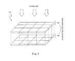
- Fig. 1 is a view showing an overview of a solid-state image sensor 101 according to the present embodiment.
- the solid-state image sensor 101 includes a first image sensor 102 that performs photoelectric conversion by using a photodiode, as with an ordinary solid-state image sensor, and a second image sensor 103 arranged on the same optical path on an incoming light side of the first image sensor 102.
- the second image sensor 103 includes an organic photoelectric conversion film which transmits specific light and photoelectrically converts non-transmitted light, and the specific light having transmitted the second image sensor 103 is received by the first image sensor 102.
- the first image sensor 102 and the second image sensor 103 are formed on the same semiconductor substrate, and each pixel position is in one-to-one correspondence to each other.
- the first row and first column pixel of the first image sensor 102 corresponds to the first row and first column pixel of the second image sensor 103.
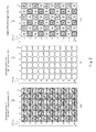
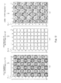
- Fig. 2(a) is a view showing an example of the pixel arrangement of the second image sensor 103.
- the horizontal direction is set to an x-axis and the vertical direction is set to a y-axis, and the coordinate of a pixel P is denoted as P(x, y).
- an organic photoelectric conversion film is alternatively arranged which photoelectrically converts the light of Mg (magenta) and Ye (yellow), while for each pixel of an even row, an organic photoelectric conversion film is alternatively arranged which photoelectrically converts the light of Cy (cyan) and Mg (magenta).
- each pixel of the second image sensor 103 includes a pixel for focus detection serving as a pair corresponding to a phase-difference AF method.
- Fig. 2(b) is a view showing an example of the pixel arrangement of the first image sensor 102. Note that, each pixel position of Fig. 2(b) is the same as that of Fig. 2(a) .
- a pixel (1, 1) of the second image sensor 103 corresponds to the pixel (1, 1) of the first image sensor 102.
- the first image sensor 102 is not provided with a color filter or the like, and photoelectrically converts the specific light transmitting the second image sensor 103 (the complementary color of light that is absorbed and photoelectrically converted by the organic photoelectric conversion film). Accordingly, as shown in Fig.
- an image of the color components of G (green) and B (blue) is obtained for each pixel of an odd row, and an image of the color components of R (red) and G (green) is obtained for each pixel of an even row.
- an image of the G component of the complementary color of Mg of the second image sensor 103 is obtained in the pixel P(1, 1).
- an image of the B component of the complementary color of Ye and an image of the R component of the complementary color of Cy are obtained, respectively.
- the second image sensor 103 including an organic photoelectric conversion film plays the role of the conventional color filter, and a complementary color image of the second image sensor 103 can be obtained by the first image sensor 102.
- a complementary color image of the second image sensor 103 can be obtained by the first image sensor 102.
- an image with a Bayer array is obtained from the first image sensor 102.
- Fig. 2 shows examples of the Bayer array, but even with other array, the same results can be achieved by arranging the first image sensor 102 and the second image sensor 103 so that each pixel of the former and each pixel of the latter have a complementary color relationship.
- the incoming light which would have been otherwise absorbed by the color filter, can be effectively utilized by the second image sensor 103.
- the solid-state image sensor 101 since a pixel for imaging is arranged in the first image sensor 102 and a pixel for focus detection is uniformly arranged overall in the second image sensor 103, there is no need to perform the complicated pixel interpolation processing, unlike the conventional art of arranging a pixel for focus detection at some of the pixels for imaging, and thus a signal for focus detection and a color image signal can be obtained from the second image sensor 103 and the first image sensor 102, respectively independently.
- Fig. 3 is a view showing a circuit example of the first image sensor 102.
- the first image sensor 102 has the pixel P(x, y) arranged in two dimensions, a vertical scanning circuit 151, a horizontal output circuit 152, and an electric current source PW. Note that, in the example of Fig. 3 , for ease of understanding, a configuration of 4 pixels of 2 rows by 2 columns is shown, but is not limiting, and actually a large number of pixels are arranged in two dimensions.
- the vertical scanning circuit 151 outputs timing signals ( ⁇ Tx(y), ⁇ R(y), ⁇ SEL(y)) for reading a signal from each pixel.
- timing signals ⁇ Tx(1), ⁇ R(1), and ⁇ SEL(1) are supplied to the pixels P(1, 1) and P(2, 1) of the first row.
- a signal is read from each pixel of vertical signal lines VLINE(1) and VLINE(2) connected to electric current sources PW(1) and PW(2) arranged in each column, respectively, and is temporarily held in the horizontal output circuit 152.
- the signal of each pixel temporarily held in the horizontal output circuit 152 for each row is sequentially output to the outside (as an output signal Vout). Note that, although not illustrated in Fig.
- a correlated double sampling (CDS circuit) for removing a variation in the signal between pixels an AD conversion circuit, a digital signal processing circuit, and the like may be arranged.
- Fig. 4 is a view showing a circuit example of the second image sensor 103.
- the second image sensor 103 has the pixel P(x, y) arranged in two dimensions, a vertical scanning circuit 161, a horizontal output circuit 162, a horizontal output circuit 163, an electric current source PW_A, and an electric current source PW_B.
- the second image sensor 103 includes 4 pixels of 2 rows by 2 columns, but not limited thereto, and actually a large number of pixels are arranged in two dimensions.
- each pixel P(x, y) of Fig. 4 corresponds to each pixel P(x, y) of Fig. 3 .
- the second image sensor 103 has, at one pixel position, two photoelectric conversion parts of a light-receiving part PC_A(x, y) and a light-receiving part PC_B(x, y) each including an organic photoelectric conversion film, and constitutes a pair of pixels serving as a pair of the phase-difference AF method.
- the vertical scanning circuit 161 outputs timing signals ( ⁇ R_A(y), ⁇ R_B(y), ⁇ SEL_A(y), and ⁇ SEL-B(y)) for reading a signal from each pixel.
- timing signals ⁇ R_A (1) and ⁇ SEL_A (1) are supplied to the light-receiving parts PC_A(1, 1) and P_A(2, 1) of the first row, and timing signals ⁇ R_B(1) and ⁇ SEL_B(1) are supplied to the light-receiving parts PC_B(1, 1) and P_B (2, 1).
- the signals of the light-receiving parts PC_A(1, 1) and P_A (2, 1) are read out to vertical signal lines VLINE_A(1) and VLINE_A(2) that are connected to the electric current sources PW_A(1) and PW_A (2) arranged at each column, respectively, and are temporarily held in a horizontal output circuit_A162.
- the signal of each pixel temporarily held in the horizontal output circuit_A162 for each row is sequentially output to the outside (as an output signal Vout_A).
- the signals of the light-receiving parts PC_B(1, 1) and P_B(2, 1) are read out to the vertical signal lines VLINE_B(1) and VLINE_B(2) that are connected to the electric current sources PW_B(1) and PW_B(2) arranged at each column, respectively, and are temporarily held in a horizontal output circuit_B162.
- the signal of each pixel temporarily held in the horizontal output circuit_B162 for each row is sequentially output to the outside (as an output signal Vout_B).
- the circuit examples of the first image sensor 102 and the second image sensor 103 have been described in Fig. 3 and Fig. 4 , respectively separately, but actually the first image sensor 102 and the second image sensor 103 are formed on the same semiconductor substrate and constitute one solid-state image sensor 101.
- Fig. 5 is a view showing a circuit example of one pixel P(x, y) arranged in two dimensions.
- the pixel P(x, y) has a photodiode PD, a transfer transistor Tx, a reset transistor R, an output transistor SF, and a selection transistor SEL as a circuit for constituting the first image sensor 102.
- the photodiode PD stores a charge corresponding to the amount of light of incoming light
- the transfer transistor Tx transfers the charge stored in the photodiode PD to a floating diffusion region (FD part) on the output transistor SF side.
- FD part floating diffusion region
- the output transistor SF constitutes the electric current source PW and a source follower via the selection transistor SEL, and outputs, to the vertical signal line VLINE, an electric signal corresponding to the charge stored in the FD part as an output signal OUT.
- the reset transistor R resets the charge of the FD part to a power-supply voltage Vcc.
- the circuit for constituting the second image sensor 103 has a light-receiving part PC including an organic photoelectric conversion film, reset transistors R_A and R_B, output transistors SF_A and SF_B, and selection transistors SEL_A and SEL_B.
- the light-receiving part PC including an organic photoelectric conversion film converts non-transmitted light into an electric signal corresponding to the amount of the non-transmitted light, as described in Fig.
- each transistor includes a MOS_FET.
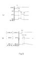
- Fig. 6 is a view showing an example of the timing signal of Fig. 5 .
- Fig. 6(a) is a view showing an operation timing of the first image sensor 102, in which, first, a selection signal ⁇ SEL becomes "High” at a timing T1 and the selection transistor SEL is turned on. Next, a reset signal ⁇ R becomes "High” at a timing T2, and the FD part is reset to the power-supply voltage Vcc and the output signal OUT also becomes a reset level.
- the transfer signal ⁇ Tx becomes "High” at a timing T3, and the charge stored in the photodiode PD is transferred to the FD part, and the output signal OUT starts to change in response to the charge amount and is then stabilized. Then, the transfer signal ⁇ Tx becomes "Low”, and the signal level of the output signal OUT to be read from a pixel to the vertical signal line VLINE is established. Then, the output signal OUT of each pixel read out to the vertical signal line VLINE is temporarily held in the horizontal output circuit_152 for each row, and, after that, is output from the solid-state image sensor 101 as the output signal Vout. In this manner, a signal is read from each pixel of the first image sensor 102.
- Fig. 6(b) is a view showing an operation timing of the second image sensor 103, wherein first, the selection signal ⁇ SEL_A (or ⁇ SEL_B) becomes "High” at a timing T11, and the selection transistor SEL_A (or SEL_B) is turned on. Next, the reset signal ⁇ R_A (or ⁇ R-B) becomes "High” at a timing T12, and the output signal OUT_A (or ⁇ OUT_B) is also set to the reset level.
- the reset signal ⁇ R_A (or ⁇ R-B) becomes "Low” at a timing T13, the charge accumulation of the light-receiving part PC by an organic photoelectric conversion film is started, and the output signal OUT_A (or output signal OUT_B) changes in response to the charge amount. Then, the resulting output signal OUT_A (or output signal OUT_B) is temporarily held in the horizontal output circuit_A162 (or horizontal output circuit_B163) for each row, and is then output from the solid-state image sensor 101 as the output signal Vout_A (or output signal Vout_B). In this manner, a signal is read from each pixel of the second image sensor 103.
- Fig. 7(a) is an example of the semiconductor layout of the solid-state image sensor 101. Note that Fig. 7(a) corresponds to each of the pixel P(1, 1) to the pixel P(2, 2) of Fig. 2 and Fig. 4 described earlier.
- Fig. 7(b) is a cross-sectional view of Fig. 7(a) along a cutout line A-B in the horizontal direction on the pixel P(1, 1) and the pixel (2, 1).
- Fig. 8(a) is an enlarged view of Fig. 7(b)
- Fig. 8(b) is a view illustrating the pixel positions along the cutout line A-B for ease of understanding.
- the pixel P(1, 1) at the same position of the first image sensor 102 and the second image sensor 103 receives incoming light from an object input from a same micro lens ML(1, 1).
- Fig. 7(b) is a cross-sectional view of Fig. 7(a) along a cutout line A-B in the horizontal direction on the pixel P(1, 1) and the pixel (2, 1).
- Fig. 8(a) is an enlarged view of Fig. 7(b)
- Fig. 8(b) is a view illustrating the pixel positions along the cutout line
- a wiring layer 301 has a three-layer structure, but it may have a two-layer structure or may have a four or more layer structure. Then, the output signal of the second image sensor 103 is extracted from a signal output end 302 via the wiring layer 301. Note that, on both sides of the signal output end 302, there are arranged separation layers 303 and 304. Moreover, at a distance from the separation layers 303 and 304, there are arranged photodiodes PD(1, 1) and PD(2, 1).
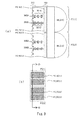
- Fig. 7(c) is a cross-sectional view of Fig. 7(a) along a cutout line C-D in the vertical direction on the pixel P(2, 1) and the pixel (2, 2). Furthermore, Fig. 9(a) is an enlarged view of Fig. 7(c) , and Fig. 9(b) is a view illustrating the pixel positions along the cutout line C-D for ease of understanding.
- the pixel P(2, 1) and pixel P(2, 2) at the same positions of the first image sensor 102 and the second image sensor 103 receive incoming light from an object input from the same micro lenses ML(2, 1) and ML(2, 2), respectively.
- Fig. 9(b) differs from Fig.
- the light-receiving part is pupil-divided into the light-receiving part PC_A(2, 1) and the light-receiving part PC_B(2, 1), and in that in the pixel P(2, 2), the light-receiving part is pupil-divided into the light-receiving part PC_A(2, 2) and the light-receiving part PC_B(2, 2).
- the light-receiving part PC_A(2, 1) and the light-receiving part PC_B(2, 1) can receive an image, serving as a pair, at a pupil position of the optical system, respectively, and perform focus detection by using a phase-difference AF method.
- the light-receiving part PC_A(2, 2) and the light-receiving part PC_B(2, 2) receive an image, serving as a pair, at the pupil position of the optical system, respectively. Note that, since the phase-difference AF method is a well-known technique, the detailed description thereof is omitted.
- the wiring layer 301 of Fig. 8(a) corresponds to a wiring layer 301 A and a wiring layer 301 B.
- the wiring layer 301 A outputs a signal of the light-receiving part PC_A(2, 1) of an organic photoelectric conversion film to the signal output end 305A
- the wiring layer 301 B outputs a signal of the light-receiving part PC_B(2, 1) of an organic photoelectric conversion film to the signal output end 305B.
- the wiring layer 301 of Fig. 8(a) only one wiring layer is visible because the wiring layer 301 A and the wiring layer 301 B overlap with each other.
- a signal of the light-receiving part PC_A(2, 2) of an organic photoelectric conversion film of the pixel P(2, 2) is output to a signal output end 306A
- a signal of the light-receiving part PC_B(2, 2) is output to a signal output end 306B.
- readout circuits such as an output transistor, a selection transistor, a reset transistor, and the like are arranged, in which the signal of each pixel is output to the outside from the solid-state image sensor 101.
- Fig. 10 is an enlarged view of the layout drawing of the pixel P(1, 1) of Fig. 7(a) .
- a hatched portion indicates a gate electrode
- white portions on both sides of the gate electrode indicate an NMOS type transistor including an n region.
- the charge stored in the photodiode PD of the first image sensor 102 is transferred to the FD part when the transfer signal ⁇ Tx is supplied to the gate electrode of the transfer transistor.
- the FD part is connected to the gate electrode of the output transistor SF, in which the transferred charge is converted into an electric signal, and when the selection signal ⁇ SEL is supplied to the gate electrode of the selection transistor SEL, the converted electric signal is read out to the vertical signal line VLINE. Note that, when the reset signal ⁇ R is supplied to the gate electrode of the reset transistor R, the charge of the FD part is reset to the power-supply voltage Vcc.
- an electric signal output from a transparent electrode of the light-receiving part PC_A(1, 1) of an organic photoelectric conversion film is connected to the gate electrode of the output transistor SF_A, and when the selection signal ⁇ SEL_A is supplied to the gate electrode of the selection transistor SEL_A, the electric signal is read out to the vertical signal line VLINE_A.
- an electric signal output from the transparent electrode of the light-receiving part PC_B(1, 1) is connected to the gate electrode of the output transistor SF_B, and when the selection signal ⁇ SEL_B is supplied to the gate electrode of the selection transistor SEL_B, the electric signal is read out to the vertical signal line VLINE_B.
- the reset signal ⁇ R_A (or ⁇ R-B) is supplied to the gate electrode of the reset transistor R_A (or R_B)
- the signal voltage of the light-receiving part PC_A(1, 1) (or PC_B(1, 1)) is reset to the reference voltage Vref.
- the high voltage Vpc for extracting an electric signal corresponding to an incoming light quantity from an opposing transparent electrode is supplied to a transparent electrode on an incoming light side.
- the solid-state image sensor 101 has the first image sensor 102 performing photoelectric conversion by using a conventional photodiode and the second image sensor 103 performing photoelectric conversion by using an organic photoelectric conversion film, wherein a signal for imaging can be acquired from the first image sensor 102 and a signal for focus detection corresponding to a phase-difference AF method can be acquired from the second image sensor 103.
- the solid-state image sensor 101 there is no need to arrange a pixel for focus detection at some of the pixels for imaging, unlike the conventional art, and there is no degradation in image quality due to a spurious signal of a vertical stripe or a horizontal stripe, and sophisticated pixel interpolation processing is not required.
- the first image sensor 102 for imaging and the second image sensor 103 for focus detection are stacked in layers so as to use incoming light of the same micro lens, a complicated optical system for dividing the incoming light into the light for an image sensor for imaging and the light for an image sensor for focus detection is not required, unlike the conventional art.
- the solid-state image sensor 101 according to the present embodiment does not require an optical device such as a prism or a mirror, while using two image sensors of the first image sensor 102 and the second image sensor 103, the arrangement and design of an optical system in configuring a camera are easy. Furthermore, in a dual-plate type imaging sensor using a prism, a mirror, and the like, adjustment and the like of the optical path length between two image sensors is indispensable, while in the solid-state image sensor 101 according to the present embodiment, the adjustment is not required because there is one optical path.
- the second image sensor 103 and the first image sensor 102 can detect color components having a complementary color relationship with each other, and the organic photoelectric conversion film of the second image sensor 103 can also be used as a color filter of the first image sensor 102, and incoming light can be efficiently used without being wasted.
- the solid-state image sensor 101 can realize a phase-difference AF method allowing for high-speed operation, without using sophisticated pixel interpolation processing and a complicated optical system.
- a phase-difference AF method capable of finding a focusing position at high speed is realized using the second image sensor 103, but a focusing position may be found by a contrast method through the use of the second image sensor 103.
- the contrast method is a method including the steps of: moving a focus lens while detecting the contrast of an image; and setting the position of a focus lens having the highest contrast, to a focusing position.
- the contrast may be calculated by adding two light-receiving parts (e.g., PC_A(x, y) and PC_B(x, y) of Fig. 11(a) ) provided in each pixel, or the light-receiving part of a pixel of the second image sensor 103 may be set to one light-receiving part without being divided.
- two light-receiving parts e.g., PC_A(x, y) and PC_B(x, y) of Fig. 11(a)
- the light-receiving parts PC_A(x, y) and PC_B(x, y) serving as a pair corresponding to the phase-difference AF method are arranged in each pixel P(x, y) of the second image sensor 103.
- both the two light-receiving parts of each pixel have been described as outputting a signal as a focus detection signal, but are not limited thereto.
- two light-receiving parts of each pixel may be constructed so that a signal is output only from either one of light-receiving parts.
- light-receiving parts, where adjacent pixels are read are light-receiving parts at mutually different positions of two light-receiving parts. In this manner, read-out drive of a signal can be performed in a conventional manner.
- a half of the light-receiving part PC_A(x, y) or the light-receiving part PC_B(x, y) may be arranged in one pixel P(x, y). That is, in Fig. 11(b) , AF control by the phase difference detection method can be performed, in which the pixel P(1, 1) having the light-receiving part PC_A(1, 1) arranged on the left side and the pixel P(2, 1) having the light-receiving part PC_B(2, 1) arranged on the right side are paired.
- the pixels for focus detection whose pupil division directions are various directions such as a vertical direction, a horizontal direction, and a diagonal direction may exist mixedly.
- the solid-state image sensor 101 captures a signal for imaging by the first image sensor 102 and captures a signal for focus detection by the second image sensor 103, and thus focus detection by high-speed phase-difference AF can be performed at any position in a captured image without affecting the image quality of the captured image.
- focus detection by the phase-difference AF method may be performed utilizing a signal for focus detection obtained from a pixel of the same color component.
- a signal for focus detection obtained from a pixel a pixel of an odd number column in the case of an odd row, and a pixel of an even number column in the case of an even row
- Mg a large number of pixels
- an error between the pixels corresponding to three colors of Mg, Ye, and Cy (a variation in sensitivity between pixels, a variation (DC offset) in reference level, or the like) is measured in advance, and error correction may be made when performing phase-difference AF processing.
- the output signal of the second image sensor 103 may be utilized not only for focus detection but also for white balance control.
- Fig. 12 is a view showing Modification 1 of the color array of a pixel described in Fig. 2 .
- the organic photoelectric conversion film of the second image sensor 103 is adapted to correspond to three colors of Mg, Ye, and Cy, and an image signal of three colors of R, G, and B can be detected by the first image sensor 102.
- the organic photoelectric conversion film of the second image sensor 103 may correspond to three colors of R, G, and B, and an image signal of three colors of Mg, Ye, and Cy may be detected by the first image sensor 102.
- a color component the first image sensor 102 photoelectrically converts and a color component the second image sensor 103 photoelectrically converts have a complementary color relationship with each other.
- Fig. 13 is a view showing Modification 2 of the color array of a pixel described in Fig. 2 .
- a light-receiving part serving as a pair corresponding to the phase-difference AF method is arranged in each pixel of the second image sensor 103, while in the modifications of Fig. 13 , a light-receiving part serving as a pair corresponding to the phase-difference AF method is arranged in some of the pixels of the second image sensor 103. Therefore, the circuit size of the solid-state image sensor 101 can be reduced.
- the electronic camera 101 includes an optical system 202, the solid-state image sensor 101, an image buffer 203, an image processing part 204, a controller 205, a display part 206, a memory 207, an operation part 208, and a memory card IF209.
- the optical system 202 forms an object image on the solid-state image sensor 101.
- the solid-state image sensor 101 has the first image sensor 102 and the second image sensor 103, as described earlier, a signal for imaging captured by the first image sensor 102 is taken in the image buffer 203, and a signal for focus detection acquired by the second image sensor 103 is input to the controller 205.
- the controller 205 controls the whole electronic camera 201 in response to a user operation using the operation part 208. For example, when a release button of the operation part 208 is half-pressed, the controller 205 performs focus detection by the phase-difference AF method through the use of the signal for focus detection obtained from the second image sensor, and controls the focusing position of the optical system 202.
- the controller 205 takes an image captured by the first image sensor 102 after the focus control, in the image buffer 203. Furthermore, the image taken in the image buffer 203 is subjected to white balance processing, color interpolation processing, contour enhancement processing, gamma correction processing, and the like by the image processing part 204, and is displayed on the display part 206 or stored into the memory card 209 via the memory card IF209.
- the second image sensor 103 outputs a signal for imaging, as with the first image sensor 102. Then, the controller 205 moves the focus lens of the optical system 202 while detecting the contrast of the signal for imaging which the second image sensor 103 outputs, and obtains a position of the focus lens, where the highest contrast is obtained, and sets this position to the focusing position.
Landscapes
- Engineering & Computer Science (AREA)
- Multimedia (AREA)
- Signal Processing (AREA)
- Physics & Mathematics (AREA)
- Spectroscopy & Molecular Physics (AREA)
- General Physics & Mathematics (AREA)
- Optics & Photonics (AREA)
- Inorganic Chemistry (AREA)
- Chemical & Material Sciences (AREA)
- Transforming Light Signals Into Electric Signals (AREA)
- Solid State Image Pick-Up Elements (AREA)
- Automatic Focus Adjustment (AREA)
- Focusing (AREA)
- Color Television Image Signal Generators (AREA)
- Electromagnetism (AREA)
- Studio Devices (AREA)
Applications Claiming Priority (2)
| Application Number | Priority Date | Filing Date | Title |
|---|---|---|---|
| JP2012005270A JP5556823B2 (ja) | 2012-01-13 | 2012-01-13 | 固体撮像装置および電子カメラ |
| PCT/JP2013/000012 WO2013105481A1 (ja) | 2012-01-13 | 2013-01-08 | 固体撮像装置および電子カメラ |
Publications (3)
| Publication Number | Publication Date |
|---|---|
| EP2804035A1 true EP2804035A1 (de) | 2014-11-19 |
| EP2804035A4 EP2804035A4 (de) | 2015-10-28 |
| EP2804035B1 EP2804035B1 (de) | 2020-04-15 |
Family
ID=48779720
Family Applications (1)
| Application Number | Title | Priority Date | Filing Date |
|---|---|---|---|
| EP13735697.8A Active EP2804035B1 (de) | 2012-01-13 | 2013-01-08 | Festkörper-bildaufnahmevorrichtung und elektronische kamera |
Country Status (8)
| Country | Link |
|---|---|
| US (5) | US9385148B2 (de) |
| EP (1) | EP2804035B1 (de) |
| JP (1) | JP5556823B2 (de) |
| KR (2) | KR101755084B1 (de) |
| CN (7) | CN107197179B (de) |
| BR (1) | BR112014016988A2 (de) |
| RU (1) | RU2602754C2 (de) |
| WO (1) | WO2013105481A1 (de) |
Cited By (4)
| Publication number | Priority date | Publication date | Assignee | Title |
|---|---|---|---|---|
| JP2016152417A (ja) * | 2015-02-16 | 2016-08-22 | 三星電子株式会社Samsung Electronics Co.,Ltd. | イメージセンサ、及びイメージセンサを含む撮像装置 |
| US10535687B2 (en) | 2015-01-22 | 2020-01-14 | Sony Semiconductor Solutions Corporation | Solid-state imaging device and electronic apparatus |
| US10692904B2 (en) | 2015-03-13 | 2020-06-23 | Sony Semiconductor Solutions Corporation | Solid-state image sensing device, drive method, and electronic apparatus |
| US10715753B2 (en) | 2016-05-11 | 2020-07-14 | Sony Corporation | Solid-state image pickup element and electronic apparatus |
Families Citing this family (60)
| Publication number | Priority date | Publication date | Assignee | Title |
|---|---|---|---|---|
| JP5556823B2 (ja) * | 2012-01-13 | 2014-07-23 | 株式会社ニコン | 固体撮像装置および電子カメラ |
| CN111711746A (zh) | 2012-03-30 | 2020-09-25 | 株式会社尼康 | 摄像装置以及摄像元件 |
| JP2014203070A (ja) * | 2013-04-10 | 2014-10-27 | 日本放送協会 | オートフォーカス用センサ、及び、オートフォーカス装置 |
| WO2014171284A1 (ja) * | 2013-04-19 | 2014-10-23 | オリンパスメディカルシステムズ株式会社 | 内視鏡装置 |
| JP6232589B2 (ja) * | 2013-06-24 | 2017-11-22 | パナソニックIpマネジメント株式会社 | 固体撮像装置およびその製造方法 |
| JP6136669B2 (ja) * | 2013-07-08 | 2017-05-31 | 株式会社ニコン | 撮像装置 |
| JP6368993B2 (ja) * | 2013-07-24 | 2018-08-08 | 株式会社ニコン | 撮像装置 |
| JP6108172B2 (ja) * | 2013-09-02 | 2017-04-05 | ソニー株式会社 | 固体撮像素子およびその製造方法、並びに電子機器 |
| CN110225270A (zh) * | 2013-10-02 | 2019-09-10 | 株式会社尼康 | 摄像元件以及摄像装置 |
| JP6305006B2 (ja) * | 2013-10-18 | 2018-04-04 | キヤノン株式会社 | 撮像装置、撮像システム、撮像装置の制御方法、プログラム、および、記憶媒体 |
| JP2015099862A (ja) * | 2013-11-19 | 2015-05-28 | 株式会社東芝 | 固体撮像装置および固体撮像装置の製造方法 |
| JP6458343B2 (ja) * | 2014-02-27 | 2019-01-30 | 株式会社ニコン | 撮像装置 |
| JP2015207594A (ja) * | 2014-04-17 | 2015-11-19 | パナソニックIpマネジメント株式会社 | 固体撮像装置 |
| US9432568B2 (en) * | 2014-06-30 | 2016-08-30 | Semiconductor Components Industries, Llc | Pixel arrangements for image sensors with phase detection pixels |
| US10554874B2 (en) | 2014-07-22 | 2020-02-04 | Sony Semiconductor Solutions Corporation | Solid-state imaging device and electronic equipment |
| JP6682175B2 (ja) * | 2014-07-31 | 2020-04-15 | キヤノン株式会社 | 固体撮像素子および撮像システム |
| JP6521586B2 (ja) * | 2014-07-31 | 2019-05-29 | キヤノン株式会社 | 固体撮像素子および撮像システム |
| JP2016058559A (ja) | 2014-09-10 | 2016-04-21 | ソニー株式会社 | 固体撮像装置およびその駆動方法、並びに電子機器 |
| US9967501B2 (en) | 2014-10-08 | 2018-05-08 | Panasonic Intellectual Property Management Co., Ltd. | Imaging device |
| TWI692090B (zh) | 2014-11-05 | 2020-04-21 | 日商索尼半導體解決方案公司 | 固體攝像元件及其製造方法 |
| TWI700824B (zh) * | 2015-02-09 | 2020-08-01 | 日商索尼半導體解決方案公司 | 攝像元件及電子裝置 |
| JP6578702B2 (ja) * | 2015-03-30 | 2019-09-25 | 株式会社ニコン | 撮像素子および撮像装置 |
| JP6536126B2 (ja) | 2015-03-31 | 2019-07-03 | 株式会社ニコン | 撮像素子および撮像装置 |
| JP2016191875A (ja) * | 2015-03-31 | 2016-11-10 | 株式会社ニコン | 焦点検出装置および撮影装置 |
| CN108140655A (zh) * | 2015-09-25 | 2018-06-08 | 株式会社尼康 | 拍摄元件以及拍摄装置 |
| KR102466671B1 (ko) * | 2015-10-02 | 2022-11-14 | 삼성전자주식회사 | 적층형 이미지 센서 |
| KR102491497B1 (ko) | 2015-11-30 | 2023-01-20 | 삼성전자주식회사 | 이미지 센서 및 이를 포함하는 전자 장치 |
| JP2017103420A (ja) * | 2015-12-04 | 2017-06-08 | 株式会社ニコン | 撮像素子 |
| US10546898B2 (en) | 2015-12-24 | 2020-01-28 | Sony Corporation | Imaging apparatus and electronic device |
| CN108702472A (zh) * | 2016-01-08 | 2018-10-23 | 株式会社尼康 | 摄像装置及电子相机 |
| JP6750635B2 (ja) * | 2016-01-08 | 2020-09-02 | 株式会社ニコン | 撮像素子および撮像装置 |
| JPWO2017119477A1 (ja) * | 2016-01-08 | 2018-11-22 | 株式会社ニコン | 撮像素子および撮像装置 |
| JP6782431B2 (ja) * | 2016-01-22 | 2020-11-11 | パナソニックIpマネジメント株式会社 | 撮像装置 |
| CN112788225B (zh) | 2016-01-29 | 2023-01-20 | 松下知识产权经营株式会社 | 摄像装置 |
| JP2017152658A (ja) * | 2016-02-26 | 2017-08-31 | 株式会社ニコン | 撮像素子および撮像装置 |
| US10063763B2 (en) * | 2016-07-07 | 2018-08-28 | Tdk Taiwan Corp. | Camera module |
| CN109791935A (zh) * | 2016-09-29 | 2019-05-21 | 株式会社尼康 | 摄像元件、焦点检测装置及电子相机 |
| CN108337409B (zh) * | 2017-01-19 | 2021-06-22 | 松下知识产权经营株式会社 | 摄像装置及照相机系统 |
| US10271037B2 (en) | 2017-01-20 | 2019-04-23 | Semiconductor Components Industries, Llc | Image sensors with hybrid three-dimensional imaging |
| US10075663B2 (en) | 2017-01-20 | 2018-09-11 | Semiconductor Components Industries, Llc | Phase detection pixels with high speed readout |
| WO2018186302A1 (ja) * | 2017-04-05 | 2018-10-11 | 株式会社ニコン | 撮像素子および撮像装置 |
| CN106973206B (zh) * | 2017-04-28 | 2020-06-05 | Oppo广东移动通信有限公司 | 摄像模组摄像处理方法、装置和终端设备 |
| KR102514047B1 (ko) | 2018-02-20 | 2023-03-24 | 삼성전자주식회사 | 복수의 기능이 통합된 이미지 센서 및 이를 포함하는 이미지 센서 모듈 |
| JP2018160936A (ja) * | 2018-07-12 | 2018-10-11 | 株式会社ニコン | 撮像装置 |
| JP2019086785A (ja) * | 2018-12-27 | 2019-06-06 | 株式会社ニコン | 撮像素子および撮像装置 |
| JP7378935B2 (ja) | 2019-02-06 | 2023-11-14 | キヤノン株式会社 | 画像処理装置 |
| JP7134911B2 (ja) * | 2019-04-22 | 2022-09-12 | キヤノン株式会社 | 固体撮像素子および撮像システム |
| FR3098990A1 (fr) * | 2019-07-19 | 2021-01-22 | Isorg | Pixel de capteur d’images |
| FR3098989B1 (fr) * | 2019-07-19 | 2023-08-25 | Isorg | Pixel de capteur d’images |
| FR3098991B1 (fr) * | 2019-07-19 | 2023-08-25 | Isorg | Pixel de capteur d’images |
| EP4075793A4 (de) * | 2019-12-10 | 2023-01-04 | Sony Semiconductor Solutions Corporation | Bildgebungsvorrichtung und elektronisches gerät |
| JP7071416B2 (ja) * | 2020-01-29 | 2022-05-18 | キヤノン株式会社 | 固体撮像素子および撮像システム |
| KR102825030B1 (ko) | 2020-07-20 | 2025-06-24 | 삼성전자주식회사 | 이미지 센서 및 전자 장치 |
| JP2022049487A (ja) * | 2020-09-16 | 2022-03-29 | ソニーグループ株式会社 | 固体撮像装置及び電子機器 |
| KR102778978B1 (ko) | 2020-11-18 | 2025-03-11 | 삼성전자주식회사 | 카메라 모듈 및 카메라 모듈을 포함하는 전자 장치 |
| US11477364B1 (en) | 2021-04-01 | 2022-10-18 | Visera Technologies Company Limited | Solid-state image sensor |
| KR102902655B1 (ko) | 2021-05-18 | 2025-12-19 | 삼성전자주식회사 | 이미지 센서 및 상기 이미지 센서를 포함하는 이미지 센싱 시스템 |
| CN117501704A (zh) * | 2021-09-28 | 2024-02-02 | 华为技术有限公司 | 一种摄像头模组及电子设备 |
| CN117256159B (zh) * | 2022-04-15 | 2025-10-17 | 北京小米移动软件有限公司 | 固体拍摄装置以及摄像头设备 |
| JP2024012869A (ja) * | 2022-07-19 | 2024-01-31 | 株式会社シグマ | 撮像装置及び撮像装置の画像データ読み出し方法 |
Family Cites Families (59)
| Publication number | Priority date | Publication date | Assignee | Title |
|---|---|---|---|---|
| JPS62230165A (ja) * | 1986-03-31 | 1987-10-08 | Ricoh Co Ltd | 2色原稿読取装置 |
| EP2295238A1 (de) * | 1998-08-19 | 2011-03-16 | The Trustees Of Princeton University | Organische lichtempfindliche optoelektronische Vorrichtung |
| JP2001021792A (ja) | 1999-07-09 | 2001-01-26 | Olympus Optical Co Ltd | 焦点検出システム |
| JP2003219259A (ja) * | 2002-01-23 | 2003-07-31 | Fuji Photo Film Co Ltd | デジタルカメラにおける片ぼけの補正方法及びデジタルカメラ |
| JP2004200902A (ja) | 2002-12-17 | 2004-07-15 | Nikon Corp | 画像処理装置、電子カメラ、及び画像処理プログラム |
| US6958862B1 (en) * | 2003-04-21 | 2005-10-25 | Foveon, Inc. | Use of a lenslet array with a vertically stacked pixel array |
| KR100659532B1 (ko) * | 2003-11-28 | 2006-12-19 | 삼성에스디아이 주식회사 | 평판표시장치 및 그의 제조방법 |
| JP4500706B2 (ja) | 2005-02-23 | 2010-07-14 | 富士フイルム株式会社 | 光電変換膜積層型固体撮像素子 |
| JP2007011070A (ja) | 2005-06-30 | 2007-01-18 | Olympus Imaging Corp | デジタル一眼レフカメラ |
| JP2007067075A (ja) * | 2005-08-30 | 2007-03-15 | Nippon Hoso Kyokai <Nhk> | カラー撮像素子 |
| JP4511442B2 (ja) * | 2005-09-30 | 2010-07-28 | 富士フイルム株式会社 | 感度可変型撮像素子及びこれを搭載した撮像装置 |
| US7419844B2 (en) * | 2006-03-17 | 2008-09-02 | Sharp Laboratories Of America, Inc. | Real-time CMOS imager having stacked photodiodes fabricated on SOI wafer |
| JP4449936B2 (ja) * | 2006-03-31 | 2010-04-14 | ソニー株式会社 | 撮像装置、カメラシステムおよびその駆動方法 |
| JP4807131B2 (ja) | 2006-04-05 | 2011-11-02 | 株式会社ニコン | 撮像素子および撮像装置 |
| US7711261B2 (en) | 2006-04-11 | 2010-05-04 | Nikon Corporation | Imaging device, camera and image processing method |
| JP4935162B2 (ja) | 2006-04-11 | 2012-05-23 | 株式会社ニコン | 撮像装置、カメラおよび画像処理方法 |
| JP4866656B2 (ja) | 2006-05-18 | 2012-02-01 | 富士フイルム株式会社 | 光電変換膜積層型カラー固体撮像装置 |
| JP2007324405A (ja) | 2006-06-01 | 2007-12-13 | Fujifilm Corp | 固体撮像素子 |
| JP4867552B2 (ja) * | 2006-09-28 | 2012-02-01 | 株式会社ニコン | 撮像装置 |
| JP4321579B2 (ja) * | 2006-11-28 | 2009-08-26 | ソニー株式会社 | 撮像装置 |
| US7859588B2 (en) * | 2007-03-09 | 2010-12-28 | Eastman Kodak Company | Method and apparatus for operating a dual lens camera to augment an image |
| US7676146B2 (en) * | 2007-03-09 | 2010-03-09 | Eastman Kodak Company | Camera using multiple lenses and image sensors to provide improved focusing capability |
| JP2008258474A (ja) | 2007-04-06 | 2008-10-23 | Sony Corp | 固体撮像装置および撮像装置 |
| JP4386096B2 (ja) * | 2007-05-18 | 2009-12-16 | ソニー株式会社 | 画像入力処理装置、および、その方法 |
| CN101345248B (zh) | 2007-07-09 | 2010-07-14 | 博立码杰通讯(深圳)有限公司 | 多光谱感光器件及其制作方法 |
| WO2009020031A1 (en) | 2007-08-06 | 2009-02-12 | Canon Kabushiki Kaisha | Image sensing apparatus |
| EP2179581B1 (de) * | 2007-08-10 | 2015-11-11 | Canon Kabushiki Kaisha | Bildaufnahmevorrichtung und steuerverfahren dafür |
| JP5171178B2 (ja) * | 2007-09-13 | 2013-03-27 | 富士フイルム株式会社 | イメージセンサ及びその製造方法 |
| US8022493B2 (en) * | 2007-09-27 | 2011-09-20 | Dongbu Hitek Co., Ltd. | Image sensor and manufacturing method thereof |
| JP2009099867A (ja) * | 2007-10-18 | 2009-05-07 | Fujifilm Corp | 光電変換素子及び撮像素子 |
| JP5032954B2 (ja) | 2007-11-27 | 2012-09-26 | 日本放送協会 | カラー撮像装置 |
| US8106426B2 (en) * | 2008-02-04 | 2012-01-31 | Sharp Laboratories Of America, Inc. | Full color CMOS imager filter |
| JP5298638B2 (ja) * | 2008-02-14 | 2013-09-25 | 株式会社ニコン | 画像処理装置、撮像装置、補正係数算出方法及び画像処理プログラム |
| WO2009104417A1 (ja) * | 2008-02-22 | 2009-08-27 | パナソニック株式会社 | 撮像装置 |
| JP5276371B2 (ja) | 2008-07-09 | 2013-08-28 | キヤノン株式会社 | 撮像装置 |
| JP5593602B2 (ja) * | 2008-09-24 | 2014-09-24 | ソニー株式会社 | 撮像素子および撮像装置 |
| JP5392533B2 (ja) * | 2008-10-10 | 2014-01-22 | ソニー株式会社 | 固体撮像素子、光学装置、信号処理装置及び信号処理システム |
| CN102077577B (zh) * | 2008-10-28 | 2013-05-15 | 松下电器产业株式会社 | 摄像组件 |
| KR101342968B1 (ko) * | 2008-11-27 | 2013-12-19 | 캐논 가부시끼가이샤 | 고체촬상소자 및 촬상장치 |
| JP2010141140A (ja) | 2008-12-11 | 2010-06-24 | Nippon Hoso Kyokai <Nhk> | カラーイメージセンサ |
| US20100157117A1 (en) * | 2008-12-18 | 2010-06-24 | Yu Wang | Vertical stack of image sensors with cutoff color filters |
| KR20110003169A (ko) * | 2009-07-03 | 2011-01-11 | 삼성전자주식회사 | 컬러유닛 및 이를 포함한 촬상소자 |
| FR2947952B1 (fr) * | 2009-07-07 | 2011-11-25 | Commissariat Energie Atomique | Dispositif photo-detecteur et procede de realisation de dispositif photo-detecteur |
| JP5671789B2 (ja) | 2009-08-10 | 2015-02-18 | ソニー株式会社 | 固体撮像装置とその製造方法および撮像装置 |
| US8624875B2 (en) * | 2009-08-24 | 2014-01-07 | Semiconductor Energy Laboratory Co., Ltd. | Method for driving touch panel |
| JP5537905B2 (ja) * | 2009-11-10 | 2014-07-02 | 富士フイルム株式会社 | 撮像素子及び撮像装置 |
| KR101709941B1 (ko) * | 2009-12-02 | 2017-02-27 | 삼성전자주식회사 | 이미지 센서, 이를 포함하는 이미지 처리 장치, 및 이미지 센서 제조 방법 |
| JP5509846B2 (ja) * | 2009-12-28 | 2014-06-04 | ソニー株式会社 | 固体撮像装置とその製造方法、及び電子機器 |
| CN201611903U (zh) * | 2010-01-08 | 2010-10-20 | 罗顿 | 一种红外线彩色数码照相机 |
| KR101643610B1 (ko) * | 2010-01-18 | 2016-07-29 | 삼성전자주식회사 | 디지털 촬영장치 및 방법 |
| KR101688523B1 (ko) * | 2010-02-24 | 2016-12-21 | 삼성전자주식회사 | 적층형 이미지 센서 |
| JP5552858B2 (ja) * | 2010-03-26 | 2014-07-16 | ソニー株式会社 | 固体撮像装置、固体撮像装置の駆動方法、及び、電子機器 |
| US20110317048A1 (en) * | 2010-06-29 | 2011-12-29 | Aptina Imaging Corporation | Image sensor with dual layer photodiode structure |
| JP2012049289A (ja) * | 2010-08-26 | 2012-03-08 | Sony Corp | 固体撮像装置とその製造方法、並びに電子機器 |
| JP5676988B2 (ja) * | 2010-09-14 | 2015-02-25 | キヤノン株式会社 | 焦点調節装置 |
| US8742309B2 (en) * | 2011-01-28 | 2014-06-03 | Aptina Imaging Corporation | Imagers with depth sensing capabilities |
| US8258560B1 (en) * | 2011-02-15 | 2012-09-04 | Aptina Imaging Corporation | Image sensors with stacked photo-diodes |
| JP5556823B2 (ja) * | 2012-01-13 | 2014-07-23 | 株式会社ニコン | 固体撮像装置および電子カメラ |
| US8569700B2 (en) * | 2012-03-06 | 2013-10-29 | Omnivision Technologies, Inc. | Image sensor for two-dimensional and three-dimensional image capture |
-
2012
- 2012-01-13 JP JP2012005270A patent/JP5556823B2/ja active Active
-
2013
- 2013-01-08 CN CN201710356584.XA patent/CN107197179B/zh active Active
- 2013-01-08 KR KR1020147022562A patent/KR101755084B1/ko active Active
- 2013-01-08 US US13/736,204 patent/US9385148B2/en active Active
- 2013-01-08 WO PCT/JP2013/000012 patent/WO2013105481A1/ja not_active Ceased
- 2013-01-08 CN CN201710356841.XA patent/CN107256876B/zh active Active
- 2013-01-08 CN CN201710356582.0A patent/CN107197178B/zh active Active
- 2013-01-08 CN CN201380005298.9A patent/CN104081245B/zh active Active
- 2013-01-08 CN CN201710356845.8A patent/CN107197142B/zh active Active
- 2013-01-08 KR KR1020177017747A patent/KR102028813B1/ko active Active
- 2013-01-08 EP EP13735697.8A patent/EP2804035B1/de active Active
- 2013-01-08 CN CN201710356430.0A patent/CN107197177B/zh active Active
- 2013-01-08 CN CN201710356863.6A patent/CN107197143B/zh active Active
- 2013-01-08 BR BR112014016988A patent/BR112014016988A2/pt not_active Application Discontinuation
- 2013-01-08 RU RU2014133174/28A patent/RU2602754C2/ru active
-
2016
- 2016-04-01 US US15/088,436 patent/US9654709B2/en active Active
-
2017
- 2017-04-12 US US15/485,596 patent/US10674102B2/en active Active
-
2020
- 2020-04-07 US US16/841,983 patent/US11588991B2/en active Active
-
2023
- 2023-01-26 US US18/101,863 patent/US12200380B2/en active Active
Cited By (4)
| Publication number | Priority date | Publication date | Assignee | Title |
|---|---|---|---|---|
| US10535687B2 (en) | 2015-01-22 | 2020-01-14 | Sony Semiconductor Solutions Corporation | Solid-state imaging device and electronic apparatus |
| JP2016152417A (ja) * | 2015-02-16 | 2016-08-22 | 三星電子株式会社Samsung Electronics Co.,Ltd. | イメージセンサ、及びイメージセンサを含む撮像装置 |
| US10692904B2 (en) | 2015-03-13 | 2020-06-23 | Sony Semiconductor Solutions Corporation | Solid-state image sensing device, drive method, and electronic apparatus |
| US10715753B2 (en) | 2016-05-11 | 2020-07-14 | Sony Corporation | Solid-state image pickup element and electronic apparatus |
Also Published As
Similar Documents
| Publication | Publication Date | Title |
|---|---|---|
| US12200380B2 (en) | Solid-state imaging device and electronic camera | |
| US10412349B2 (en) | Image sensor including phase detection pixel | |
| US8466998B2 (en) | Solid-state image sensor and imaging apparatus equipped with solid-state image sensor | |
| US20100309340A1 (en) | Image sensor having global and rolling shutter processes for respective sets of pixels of a pixel array | |
| CN103227897A (zh) | 固态图像传感器和相机系统 | |
| JP2005109370A (ja) | 固体撮像装置 | |
| JP6217794B2 (ja) | 固体撮像装置および電子カメラ | |
| JP6988874B2 (ja) | 撮像素子および撮像装置 | |
| JP5958497B2 (ja) | 固体撮像装置および電子カメラ | |
| JP6635098B2 (ja) | 撮像素子および撮像装置 | |
| JP4759396B2 (ja) | 固体撮像素子 |
Legal Events
| Date | Code | Title | Description |
|---|---|---|---|
| PUAI | Public reference made under article 153(3) epc to a published international application that has entered the european phase |
Free format text: ORIGINAL CODE: 0009012 |
|
| 17P | Request for examination filed |
Effective date: 20140626 |
|
| AK | Designated contracting states |
Kind code of ref document: A1 Designated state(s): AL AT BE BG CH CY CZ DE DK EE ES FI FR GB GR HR HU IE IS IT LI LT LU LV MC MK MT NL NO PL PT RO RS SE SI SK SM TR |
|
| DAX | Request for extension of the european patent (deleted) | ||
| RAP1 | Party data changed (applicant data changed or rights of an application transferred) |
Owner name: NIKON CORPORATION |
|
| RA4 | Supplementary search report drawn up and despatched (corrected) |
Effective date: 20150929 |
|
| RIC1 | Information provided on ipc code assigned before grant |
Ipc: H01L 27/14 20060101ALI20150923BHEP Ipc: H01L 27/146 20060101ALI20150923BHEP Ipc: G02B 7/34 20060101AFI20150923BHEP Ipc: G03B 13/36 20060101ALI20150923BHEP Ipc: H04N 5/369 20110101ALI20150923BHEP Ipc: G02B 7/28 20060101ALI20150923BHEP Ipc: H01L 27/30 20060101ALI20150923BHEP |
|
| STAA | Information on the status of an ep patent application or granted ep patent |
Free format text: STATUS: EXAMINATION IS IN PROGRESS |
|
| 17Q | First examination report despatched |
Effective date: 20180116 |
|
| GRAP | Despatch of communication of intention to grant a patent |
Free format text: ORIGINAL CODE: EPIDOSNIGR1 |
|
| STAA | Information on the status of an ep patent application or granted ep patent |
Free format text: STATUS: GRANT OF PATENT IS INTENDED |
|
| INTG | Intention to grant announced |
Effective date: 20191001 |
|
| GRAS | Grant fee paid |
Free format text: ORIGINAL CODE: EPIDOSNIGR3 |
|
| GRAJ | Information related to disapproval of communication of intention to grant by the applicant or resumption of examination proceedings by the epo deleted |
Free format text: ORIGINAL CODE: EPIDOSDIGR1 |
|
| GRAL | Information related to payment of fee for publishing/printing deleted |
Free format text: ORIGINAL CODE: EPIDOSDIGR3 |
|
| STAA | Information on the status of an ep patent application or granted ep patent |
Free format text: STATUS: EXAMINATION IS IN PROGRESS |
|
| GRAR | Information related to intention to grant a patent recorded |
Free format text: ORIGINAL CODE: EPIDOSNIGR71 |
|
| STAA | Information on the status of an ep patent application or granted ep patent |
Free format text: STATUS: GRANT OF PATENT IS INTENDED |
|
| GRAA | (expected) grant |
Free format text: ORIGINAL CODE: 0009210 |
|
| STAA | Information on the status of an ep patent application or granted ep patent |
Free format text: STATUS: THE PATENT HAS BEEN GRANTED |
|
| INTC | Intention to grant announced (deleted) | ||
| INTG | Intention to grant announced |
Effective date: 20200302 |
|
| AK | Designated contracting states |
Kind code of ref document: B1 Designated state(s): AL AT BE BG CH CY CZ DE DK EE ES FI FR GB GR HR HU IE IS IT LI LT LU LV MC MK MT NL NO PL PT RO RS SE SI SK SM TR |
|
| REG | Reference to a national code |
Ref country code: CH Ref legal event code: EP |
|
| REG | Reference to a national code |
Ref country code: DE Ref legal event code: R096 Ref document number: 602013067929 Country of ref document: DE |
|
| REG | Reference to a national code |
Ref country code: IE Ref legal event code: FG4D |
|
| REG | Reference to a national code |
Ref country code: AT Ref legal event code: REF Ref document number: 1257996 Country of ref document: AT Kind code of ref document: T Effective date: 20200515 |
|
| REG | Reference to a national code |
Ref country code: NL Ref legal event code: MP Effective date: 20200415 |
|
| REG | Reference to a national code |
Ref country code: LT Ref legal event code: MG4D |
|
| REG | Reference to a national code |
Ref country code: DE Ref legal event code: R082 Ref document number: 602013067929 Country of ref document: DE Representative=s name: VENNER SHIPLEY GERMANY LLP, DE Ref country code: DE Ref legal event code: R082 Ref document number: 602013067929 Country of ref document: DE Representative=s name: VENNER SHIPLEY LLP, DE |
|
| PG25 | Lapsed in a contracting state [announced via postgrant information from national office to epo] |
Ref country code: LT Free format text: LAPSE BECAUSE OF FAILURE TO SUBMIT A TRANSLATION OF THE DESCRIPTION OR TO PAY THE FEE WITHIN THE PRESCRIBED TIME-LIMIT Effective date: 20200415 Ref country code: NO Free format text: LAPSE BECAUSE OF FAILURE TO SUBMIT A TRANSLATION OF THE DESCRIPTION OR TO PAY THE FEE WITHIN THE PRESCRIBED TIME-LIMIT Effective date: 20200715 Ref country code: GR Free format text: LAPSE BECAUSE OF FAILURE TO SUBMIT A TRANSLATION OF THE DESCRIPTION OR TO PAY THE FEE WITHIN THE PRESCRIBED TIME-LIMIT Effective date: 20200716 Ref country code: FI Free format text: LAPSE BECAUSE OF FAILURE TO SUBMIT A TRANSLATION OF THE DESCRIPTION OR TO PAY THE FEE WITHIN THE PRESCRIBED TIME-LIMIT Effective date: 20200415 Ref country code: IS Free format text: LAPSE BECAUSE OF FAILURE TO SUBMIT A TRANSLATION OF THE DESCRIPTION OR TO PAY THE FEE WITHIN THE PRESCRIBED TIME-LIMIT Effective date: 20200815 Ref country code: NL Free format text: LAPSE BECAUSE OF FAILURE TO SUBMIT A TRANSLATION OF THE DESCRIPTION OR TO PAY THE FEE WITHIN THE PRESCRIBED TIME-LIMIT Effective date: 20200415 Ref country code: PT Free format text: LAPSE BECAUSE OF FAILURE TO SUBMIT A TRANSLATION OF THE DESCRIPTION OR TO PAY THE FEE WITHIN THE PRESCRIBED TIME-LIMIT Effective date: 20200817 Ref country code: SE Free format text: LAPSE BECAUSE OF FAILURE TO SUBMIT A TRANSLATION OF THE DESCRIPTION OR TO PAY THE FEE WITHIN THE PRESCRIBED TIME-LIMIT Effective date: 20200415 |
|
| REG | Reference to a national code |
Ref country code: AT Ref legal event code: MK05 Ref document number: 1257996 Country of ref document: AT Kind code of ref document: T Effective date: 20200415 |
|
| PG25 | Lapsed in a contracting state [announced via postgrant information from national office to epo] |
Ref country code: HR Free format text: LAPSE BECAUSE OF FAILURE TO SUBMIT A TRANSLATION OF THE DESCRIPTION OR TO PAY THE FEE WITHIN THE PRESCRIBED TIME-LIMIT Effective date: 20200415 Ref country code: BG Free format text: LAPSE BECAUSE OF FAILURE TO SUBMIT A TRANSLATION OF THE DESCRIPTION OR TO PAY THE FEE WITHIN THE PRESCRIBED TIME-LIMIT Effective date: 20200715 Ref country code: RS Free format text: LAPSE BECAUSE OF FAILURE TO SUBMIT A TRANSLATION OF THE DESCRIPTION OR TO PAY THE FEE WITHIN THE PRESCRIBED TIME-LIMIT Effective date: 20200415 Ref country code: LV Free format text: LAPSE BECAUSE OF FAILURE TO SUBMIT A TRANSLATION OF THE DESCRIPTION OR TO PAY THE FEE WITHIN THE PRESCRIBED TIME-LIMIT Effective date: 20200415 |
|
| PG25 | Lapsed in a contracting state [announced via postgrant information from national office to epo] |
Ref country code: AL Free format text: LAPSE BECAUSE OF FAILURE TO SUBMIT A TRANSLATION OF THE DESCRIPTION OR TO PAY THE FEE WITHIN THE PRESCRIBED TIME-LIMIT Effective date: 20200415 |
|
| REG | Reference to a national code |
Ref country code: DE Ref legal event code: R097 Ref document number: 602013067929 Country of ref document: DE |
|
| PG25 | Lapsed in a contracting state [announced via postgrant information from national office to epo] |
Ref country code: ES Free format text: LAPSE BECAUSE OF FAILURE TO SUBMIT A TRANSLATION OF THE DESCRIPTION OR TO PAY THE FEE WITHIN THE PRESCRIBED TIME-LIMIT Effective date: 20200415 Ref country code: DK Free format text: LAPSE BECAUSE OF FAILURE TO SUBMIT A TRANSLATION OF THE DESCRIPTION OR TO PAY THE FEE WITHIN THE PRESCRIBED TIME-LIMIT Effective date: 20200415 Ref country code: AT Free format text: LAPSE BECAUSE OF FAILURE TO SUBMIT A TRANSLATION OF THE DESCRIPTION OR TO PAY THE FEE WITHIN THE PRESCRIBED TIME-LIMIT Effective date: 20200415 Ref country code: EE Free format text: LAPSE BECAUSE OF FAILURE TO SUBMIT A TRANSLATION OF THE DESCRIPTION OR TO PAY THE FEE WITHIN THE PRESCRIBED TIME-LIMIT Effective date: 20200415 Ref country code: SM Free format text: LAPSE BECAUSE OF FAILURE TO SUBMIT A TRANSLATION OF THE DESCRIPTION OR TO PAY THE FEE WITHIN THE PRESCRIBED TIME-LIMIT Effective date: 20200415 Ref country code: CZ Free format text: LAPSE BECAUSE OF FAILURE TO SUBMIT A TRANSLATION OF THE DESCRIPTION OR TO PAY THE FEE WITHIN THE PRESCRIBED TIME-LIMIT Effective date: 20200415 Ref country code: IT Free format text: LAPSE BECAUSE OF FAILURE TO SUBMIT A TRANSLATION OF THE DESCRIPTION OR TO PAY THE FEE WITHIN THE PRESCRIBED TIME-LIMIT Effective date: 20200415 Ref country code: RO Free format text: LAPSE BECAUSE OF FAILURE TO SUBMIT A TRANSLATION OF THE DESCRIPTION OR TO PAY THE FEE WITHIN THE PRESCRIBED TIME-LIMIT Effective date: 20200415 |
|
| PLBE | No opposition filed within time limit |
Free format text: ORIGINAL CODE: 0009261 |
|
| STAA | Information on the status of an ep patent application or granted ep patent |
Free format text: STATUS: NO OPPOSITION FILED WITHIN TIME LIMIT |
|
| PG25 | Lapsed in a contracting state [announced via postgrant information from national office to epo] |
Ref country code: SK Free format text: LAPSE BECAUSE OF FAILURE TO SUBMIT A TRANSLATION OF THE DESCRIPTION OR TO PAY THE FEE WITHIN THE PRESCRIBED TIME-LIMIT Effective date: 20200415 Ref country code: PL Free format text: LAPSE BECAUSE OF FAILURE TO SUBMIT A TRANSLATION OF THE DESCRIPTION OR TO PAY THE FEE WITHIN THE PRESCRIBED TIME-LIMIT Effective date: 20200415 |
|
| 26N | No opposition filed |
Effective date: 20210118 |
|
| PG25 | Lapsed in a contracting state [announced via postgrant information from national office to epo] |
Ref country code: SI Free format text: LAPSE BECAUSE OF FAILURE TO SUBMIT A TRANSLATION OF THE DESCRIPTION OR TO PAY THE FEE WITHIN THE PRESCRIBED TIME-LIMIT Effective date: 20200415 |
|
| PG25 | Lapsed in a contracting state [announced via postgrant information from national office to epo] |
Ref country code: MC Free format text: LAPSE BECAUSE OF FAILURE TO SUBMIT A TRANSLATION OF THE DESCRIPTION OR TO PAY THE FEE WITHIN THE PRESCRIBED TIME-LIMIT Effective date: 20200415 |
|
| REG | Reference to a national code |
Ref country code: CH Ref legal event code: PL |
|
| PG25 | Lapsed in a contracting state [announced via postgrant information from national office to epo] |
Ref country code: LU Free format text: LAPSE BECAUSE OF NON-PAYMENT OF DUE FEES Effective date: 20210108 |
|
| REG | Reference to a national code |
Ref country code: BE Ref legal event code: MM Effective date: 20210131 |
|
| PG25 | Lapsed in a contracting state [announced via postgrant information from national office to epo] |
Ref country code: CH Free format text: LAPSE BECAUSE OF NON-PAYMENT OF DUE FEES Effective date: 20210131 Ref country code: LI Free format text: LAPSE BECAUSE OF NON-PAYMENT OF DUE FEES Effective date: 20210131 |
|
| PG25 | Lapsed in a contracting state [announced via postgrant information from national office to epo] |
Ref country code: IE Free format text: LAPSE BECAUSE OF NON-PAYMENT OF DUE FEES Effective date: 20210108 |
|
| PG25 | Lapsed in a contracting state [announced via postgrant information from national office to epo] |
Ref country code: BE Free format text: LAPSE BECAUSE OF NON-PAYMENT OF DUE FEES Effective date: 20210131 |
|
| PG25 | Lapsed in a contracting state [announced via postgrant information from national office to epo] |
Ref country code: HU Free format text: LAPSE BECAUSE OF FAILURE TO SUBMIT A TRANSLATION OF THE DESCRIPTION OR TO PAY THE FEE WITHIN THE PRESCRIBED TIME-LIMIT; INVALID AB INITIO Effective date: 20130108 |
|
| P01 | Opt-out of the competence of the unified patent court (upc) registered |
Effective date: 20230517 |
|
| PG25 | Lapsed in a contracting state [announced via postgrant information from national office to epo] |
Ref country code: CY Free format text: LAPSE BECAUSE OF FAILURE TO SUBMIT A TRANSLATION OF THE DESCRIPTION OR TO PAY THE FEE WITHIN THE PRESCRIBED TIME-LIMIT Effective date: 20200415 |
|
| PG25 | Lapsed in a contracting state [announced via postgrant information from national office to epo] |
Ref country code: MK Free format text: LAPSE BECAUSE OF FAILURE TO SUBMIT A TRANSLATION OF THE DESCRIPTION OR TO PAY THE FEE WITHIN THE PRESCRIBED TIME-LIMIT Effective date: 20200415 |
|
| PG25 | Lapsed in a contracting state [announced via postgrant information from national office to epo] |
Ref country code: TR Free format text: LAPSE BECAUSE OF FAILURE TO SUBMIT A TRANSLATION OF THE DESCRIPTION OR TO PAY THE FEE WITHIN THE PRESCRIBED TIME-LIMIT Effective date: 20200415 |
|
| PG25 | Lapsed in a contracting state [announced via postgrant information from national office to epo] |
Ref country code: MT Free format text: LAPSE BECAUSE OF FAILURE TO SUBMIT A TRANSLATION OF THE DESCRIPTION OR TO PAY THE FEE WITHIN THE PRESCRIBED TIME-LIMIT Effective date: 20200415 |
|
| PGFP | Annual fee paid to national office [announced via postgrant information from national office to epo] |
Ref country code: GB Payment date: 20251127 Year of fee payment: 14 |
|
| PGFP | Annual fee paid to national office [announced via postgrant information from national office to epo] |
Ref country code: FR Payment date: 20251128 Year of fee payment: 14 |
|
| PGFP | Annual fee paid to national office [announced via postgrant information from national office to epo] |
Ref country code: DE Payment date: 20251203 Year of fee payment: 14 |