EP2565951B1 - Unité électroluminescente et appareil d'éclairage - Google Patents
Unité électroluminescente et appareil d'éclairage Download PDFInfo
- Publication number
- EP2565951B1 EP2565951B1 EP11775017.4A EP11775017A EP2565951B1 EP 2565951 B1 EP2565951 B1 EP 2565951B1 EP 11775017 A EP11775017 A EP 11775017A EP 2565951 B1 EP2565951 B1 EP 2565951B1
- Authority
- EP
- European Patent Office
- Prior art keywords
- light emitting
- heat transfer
- emitting unit
- led chip
- transfer plate
- Prior art date
- Legal status (The legal status is an assumption and is not a legal conclusion. Google has not performed a legal analysis and makes no representation as to the accuracy of the status listed.)
- Active
Links
Images


Classifications
-
- H—ELECTRICITY
- H05—ELECTRIC TECHNIQUES NOT OTHERWISE PROVIDED FOR
- H05K—PRINTED CIRCUITS; CASINGS OR CONSTRUCTIONAL DETAILS OF ELECTRIC APPARATUS; MANUFACTURE OF ASSEMBLAGES OF ELECTRICAL COMPONENTS
- H05K1/00—Printed circuits
- H05K1/02—Details
- H05K1/0201—Thermal arrangements, e.g. for cooling, heating or preventing overheating
- H05K1/0203—Cooling of mounted components
-
- H—ELECTRICITY
- H01—ELECTRIC ELEMENTS
- H01L—SEMICONDUCTOR DEVICES NOT COVERED BY CLASS H10
- H01L33/00—Semiconductor devices with at least one potential-jump barrier or surface barrier specially adapted for light emission; Processes or apparatus specially adapted for the manufacture or treatment thereof or of parts thereof; Details thereof
- H01L33/48—Semiconductor devices with at least one potential-jump barrier or surface barrier specially adapted for light emission; Processes or apparatus specially adapted for the manufacture or treatment thereof or of parts thereof; Details thereof characterised by the semiconductor body packages
- H01L33/64—Heat extraction or cooling elements
-
- F—MECHANICAL ENGINEERING; LIGHTING; HEATING; WEAPONS; BLASTING
- F21—LIGHTING
- F21K—NON-ELECTRIC LIGHT SOURCES USING LUMINESCENCE; LIGHT SOURCES USING ELECTROCHEMILUMINESCENCE; LIGHT SOURCES USING CHARGES OF COMBUSTIBLE MATERIAL; LIGHT SOURCES USING SEMICONDUCTOR DEVICES AS LIGHT-GENERATING ELEMENTS; LIGHT SOURCES NOT OTHERWISE PROVIDED FOR
- F21K9/00—Light sources using semiconductor devices as light-generating elements, e.g. using light-emitting diodes [LED] or lasers
- F21K9/20—Light sources comprising attachment means
- F21K9/27—Retrofit light sources for lighting devices with two fittings for each light source, e.g. for substitution of fluorescent tubes
-
- F—MECHANICAL ENGINEERING; LIGHTING; HEATING; WEAPONS; BLASTING
- F21—LIGHTING
- F21K—NON-ELECTRIC LIGHT SOURCES USING LUMINESCENCE; LIGHT SOURCES USING ELECTROCHEMILUMINESCENCE; LIGHT SOURCES USING CHARGES OF COMBUSTIBLE MATERIAL; LIGHT SOURCES USING SEMICONDUCTOR DEVICES AS LIGHT-GENERATING ELEMENTS; LIGHT SOURCES NOT OTHERWISE PROVIDED FOR
- F21K9/00—Light sources using semiconductor devices as light-generating elements, e.g. using light-emitting diodes [LED] or lasers
- F21K9/90—Methods of manufacture
-
- F—MECHANICAL ENGINEERING; LIGHTING; HEATING; WEAPONS; BLASTING
- F21—LIGHTING
- F21V—FUNCTIONAL FEATURES OR DETAILS OF LIGHTING DEVICES OR SYSTEMS THEREOF; STRUCTURAL COMBINATIONS OF LIGHTING DEVICES WITH OTHER ARTICLES, NOT OTHERWISE PROVIDED FOR
- F21V19/00—Fastening of light sources or lamp holders
- F21V19/001—Fastening of light sources or lamp holders the light sources being semiconductors devices, e.g. LEDs
- F21V19/003—Fastening of light source holders, e.g. of circuit boards or substrates holding light sources
- F21V19/004—Fastening of light source holders, e.g. of circuit boards or substrates holding light sources by deformation of parts or snap action mountings, e.g. using clips
-
- H—ELECTRICITY
- H01—ELECTRIC ELEMENTS
- H01L—SEMICONDUCTOR DEVICES NOT COVERED BY CLASS H10
- H01L24/00—Arrangements for connecting or disconnecting semiconductor or solid-state bodies; Methods or apparatus related thereto
- H01L24/93—Batch processes
- H01L24/95—Batch processes at chip-level, i.e. with connecting carried out on a plurality of singulated devices, i.e. on diced chips
- H01L24/97—Batch processes at chip-level, i.e. with connecting carried out on a plurality of singulated devices, i.e. on diced chips the devices being connected to a common substrate, e.g. interposer, said common substrate being separable into individual assemblies after connecting
-
- H—ELECTRICITY
- H05—ELECTRIC TECHNIQUES NOT OTHERWISE PROVIDED FOR
- H05K—PRINTED CIRCUITS; CASINGS OR CONSTRUCTIONAL DETAILS OF ELECTRIC APPARATUS; MANUFACTURE OF ASSEMBLAGES OF ELECTRICAL COMPONENTS
- H05K1/00—Printed circuits
- H05K1/18—Printed circuits structurally associated with non-printed electric components
- H05K1/181—Printed circuits structurally associated with non-printed electric components associated with surface mounted components
-
- F—MECHANICAL ENGINEERING; LIGHTING; HEATING; WEAPONS; BLASTING
- F21—LIGHTING
- F21K—NON-ELECTRIC LIGHT SOURCES USING LUMINESCENCE; LIGHT SOURCES USING ELECTROCHEMILUMINESCENCE; LIGHT SOURCES USING CHARGES OF COMBUSTIBLE MATERIAL; LIGHT SOURCES USING SEMICONDUCTOR DEVICES AS LIGHT-GENERATING ELEMENTS; LIGHT SOURCES NOT OTHERWISE PROVIDED FOR
- F21K9/00—Light sources using semiconductor devices as light-generating elements, e.g. using light-emitting diodes [LED] or lasers
- F21K9/20—Light sources comprising attachment means
-
- F—MECHANICAL ENGINEERING; LIGHTING; HEATING; WEAPONS; BLASTING
- F21—LIGHTING
- F21V—FUNCTIONAL FEATURES OR DETAILS OF LIGHTING DEVICES OR SYSTEMS THEREOF; STRUCTURAL COMBINATIONS OF LIGHTING DEVICES WITH OTHER ARTICLES, NOT OTHERWISE PROVIDED FOR
- F21V29/00—Protecting lighting devices from thermal damage; Cooling or heating arrangements specially adapted for lighting devices or systems
- F21V29/50—Cooling arrangements
- F21V29/70—Cooling arrangements characterised by passive heat-dissipating elements, e.g. heat-sinks
- F21V29/74—Cooling arrangements characterised by passive heat-dissipating elements, e.g. heat-sinks with fins or blades
- F21V29/76—Cooling arrangements characterised by passive heat-dissipating elements, e.g. heat-sinks with fins or blades with essentially identical parallel planar fins or blades, e.g. with comb-like cross-section
- F21V29/767—Cooling arrangements characterised by passive heat-dissipating elements, e.g. heat-sinks with fins or blades with essentially identical parallel planar fins or blades, e.g. with comb-like cross-section the planes containing the fins or blades having directions perpendicular to the light emitting axis
-
- F—MECHANICAL ENGINEERING; LIGHTING; HEATING; WEAPONS; BLASTING
- F21—LIGHTING
- F21Y—INDEXING SCHEME ASSOCIATED WITH SUBCLASSES F21K, F21L, F21S and F21V, RELATING TO THE FORM OR THE KIND OF THE LIGHT SOURCES OR OF THE COLOUR OF THE LIGHT EMITTED
- F21Y2103/00—Elongate light sources, e.g. fluorescent tubes
- F21Y2103/10—Elongate light sources, e.g. fluorescent tubes comprising a linear array of point-like light-generating elements
-
- F—MECHANICAL ENGINEERING; LIGHTING; HEATING; WEAPONS; BLASTING
- F21—LIGHTING
- F21Y—INDEXING SCHEME ASSOCIATED WITH SUBCLASSES F21K, F21L, F21S and F21V, RELATING TO THE FORM OR THE KIND OF THE LIGHT SOURCES OR OF THE COLOUR OF THE LIGHT EMITTED
- F21Y2105/00—Planar light sources
- F21Y2105/10—Planar light sources comprising a two-dimensional array of point-like light-generating elements
-
- F—MECHANICAL ENGINEERING; LIGHTING; HEATING; WEAPONS; BLASTING
- F21—LIGHTING
- F21Y—INDEXING SCHEME ASSOCIATED WITH SUBCLASSES F21K, F21L, F21S and F21V, RELATING TO THE FORM OR THE KIND OF THE LIGHT SOURCES OR OF THE COLOUR OF THE LIGHT EMITTED
- F21Y2107/00—Light sources with three-dimensionally disposed light-generating elements
- F21Y2107/90—Light sources with three-dimensionally disposed light-generating elements on two opposite sides of supports or substrates
-
- F—MECHANICAL ENGINEERING; LIGHTING; HEATING; WEAPONS; BLASTING
- F21—LIGHTING
- F21Y—INDEXING SCHEME ASSOCIATED WITH SUBCLASSES F21K, F21L, F21S and F21V, RELATING TO THE FORM OR THE KIND OF THE LIGHT SOURCES OR OF THE COLOUR OF THE LIGHT EMITTED
- F21Y2115/00—Light-generating elements of semiconductor light sources
- F21Y2115/10—Light-emitting diodes [LED]
-
- H—ELECTRICITY
- H01—ELECTRIC ELEMENTS
- H01L—SEMICONDUCTOR DEVICES NOT COVERED BY CLASS H10
- H01L2224/00—Indexing scheme for arrangements for connecting or disconnecting semiconductor or solid-state bodies and methods related thereto as covered by H01L24/00
- H01L2224/01—Means for bonding being attached to, or being formed on, the surface to be connected, e.g. chip-to-package, die-attach, "first-level" interconnects; Manufacturing methods related thereto
- H01L2224/42—Wire connectors; Manufacturing methods related thereto
- H01L2224/44—Structure, shape, material or disposition of the wire connectors prior to the connecting process
- H01L2224/45—Structure, shape, material or disposition of the wire connectors prior to the connecting process of an individual wire connector
- H01L2224/45001—Core members of the connector
- H01L2224/45099—Material
- H01L2224/451—Material with a principal constituent of the material being a metal or a metalloid, e.g. boron (B), silicon (Si), germanium (Ge), arsenic (As), antimony (Sb), tellurium (Te) and polonium (Po), and alloys thereof
- H01L2224/45117—Material with a principal constituent of the material being a metal or a metalloid, e.g. boron (B), silicon (Si), germanium (Ge), arsenic (As), antimony (Sb), tellurium (Te) and polonium (Po), and alloys thereof the principal constituent melting at a temperature of greater than or equal to 400°C and less than 950°C
- H01L2224/45124—Aluminium (Al) as principal constituent
-
- H—ELECTRICITY
- H01—ELECTRIC ELEMENTS
- H01L—SEMICONDUCTOR DEVICES NOT COVERED BY CLASS H10
- H01L2224/00—Indexing scheme for arrangements for connecting or disconnecting semiconductor or solid-state bodies and methods related thereto as covered by H01L24/00
- H01L2224/01—Means for bonding being attached to, or being formed on, the surface to be connected, e.g. chip-to-package, die-attach, "first-level" interconnects; Manufacturing methods related thereto
- H01L2224/42—Wire connectors; Manufacturing methods related thereto
- H01L2224/44—Structure, shape, material or disposition of the wire connectors prior to the connecting process
- H01L2224/45—Structure, shape, material or disposition of the wire connectors prior to the connecting process of an individual wire connector
- H01L2224/45001—Core members of the connector
- H01L2224/45099—Material
- H01L2224/451—Material with a principal constituent of the material being a metal or a metalloid, e.g. boron (B), silicon (Si), germanium (Ge), arsenic (As), antimony (Sb), tellurium (Te) and polonium (Po), and alloys thereof
- H01L2224/45138—Material with a principal constituent of the material being a metal or a metalloid, e.g. boron (B), silicon (Si), germanium (Ge), arsenic (As), antimony (Sb), tellurium (Te) and polonium (Po), and alloys thereof the principal constituent melting at a temperature of greater than or equal to 950°C and less than 1550°C
- H01L2224/45139—Silver (Ag) as principal constituent
-
- H—ELECTRICITY
- H01—ELECTRIC ELEMENTS
- H01L—SEMICONDUCTOR DEVICES NOT COVERED BY CLASS H10
- H01L2224/00—Indexing scheme for arrangements for connecting or disconnecting semiconductor or solid-state bodies and methods related thereto as covered by H01L24/00
- H01L2224/01—Means for bonding being attached to, or being formed on, the surface to be connected, e.g. chip-to-package, die-attach, "first-level" interconnects; Manufacturing methods related thereto
- H01L2224/42—Wire connectors; Manufacturing methods related thereto
- H01L2224/44—Structure, shape, material or disposition of the wire connectors prior to the connecting process
- H01L2224/45—Structure, shape, material or disposition of the wire connectors prior to the connecting process of an individual wire connector
- H01L2224/45001—Core members of the connector
- H01L2224/45099—Material
- H01L2224/451—Material with a principal constituent of the material being a metal or a metalloid, e.g. boron (B), silicon (Si), germanium (Ge), arsenic (As), antimony (Sb), tellurium (Te) and polonium (Po), and alloys thereof
- H01L2224/45138—Material with a principal constituent of the material being a metal or a metalloid, e.g. boron (B), silicon (Si), germanium (Ge), arsenic (As), antimony (Sb), tellurium (Te) and polonium (Po), and alloys thereof the principal constituent melting at a temperature of greater than or equal to 950°C and less than 1550°C
- H01L2224/45144—Gold (Au) as principal constituent
-
- H—ELECTRICITY
- H01—ELECTRIC ELEMENTS
- H01L—SEMICONDUCTOR DEVICES NOT COVERED BY CLASS H10
- H01L2224/00—Indexing scheme for arrangements for connecting or disconnecting semiconductor or solid-state bodies and methods related thereto as covered by H01L24/00
- H01L2224/01—Means for bonding being attached to, or being formed on, the surface to be connected, e.g. chip-to-package, die-attach, "first-level" interconnects; Manufacturing methods related thereto
- H01L2224/42—Wire connectors; Manufacturing methods related thereto
- H01L2224/47—Structure, shape, material or disposition of the wire connectors after the connecting process
- H01L2224/48—Structure, shape, material or disposition of the wire connectors after the connecting process of an individual wire connector
- H01L2224/4805—Shape
- H01L2224/4809—Loop shape
- H01L2224/48091—Arched
-
- H—ELECTRICITY
- H01—ELECTRIC ELEMENTS
- H01L—SEMICONDUCTOR DEVICES NOT COVERED BY CLASS H10
- H01L2224/00—Indexing scheme for arrangements for connecting or disconnecting semiconductor or solid-state bodies and methods related thereto as covered by H01L24/00
- H01L2224/01—Means for bonding being attached to, or being formed on, the surface to be connected, e.g. chip-to-package, die-attach, "first-level" interconnects; Manufacturing methods related thereto
- H01L2224/42—Wire connectors; Manufacturing methods related thereto
- H01L2224/47—Structure, shape, material or disposition of the wire connectors after the connecting process
- H01L2224/48—Structure, shape, material or disposition of the wire connectors after the connecting process of an individual wire connector
- H01L2224/481—Disposition
- H01L2224/48135—Connecting between different semiconductor or solid-state bodies, i.e. chip-to-chip
- H01L2224/48137—Connecting between different semiconductor or solid-state bodies, i.e. chip-to-chip the bodies being arranged next to each other, e.g. on a common substrate
-
- H—ELECTRICITY
- H01—ELECTRIC ELEMENTS
- H01L—SEMICONDUCTOR DEVICES NOT COVERED BY CLASS H10
- H01L2224/00—Indexing scheme for arrangements for connecting or disconnecting semiconductor or solid-state bodies and methods related thereto as covered by H01L24/00
- H01L2224/01—Means for bonding being attached to, or being formed on, the surface to be connected, e.g. chip-to-package, die-attach, "first-level" interconnects; Manufacturing methods related thereto
- H01L2224/42—Wire connectors; Manufacturing methods related thereto
- H01L2224/47—Structure, shape, material or disposition of the wire connectors after the connecting process
- H01L2224/48—Structure, shape, material or disposition of the wire connectors after the connecting process of an individual wire connector
- H01L2224/481—Disposition
- H01L2224/48151—Connecting between a semiconductor or solid-state body and an item not being a semiconductor or solid-state body, e.g. chip-to-substrate, chip-to-passive
- H01L2224/48221—Connecting between a semiconductor or solid-state body and an item not being a semiconductor or solid-state body, e.g. chip-to-substrate, chip-to-passive the body and the item being stacked
- H01L2224/48225—Connecting between a semiconductor or solid-state body and an item not being a semiconductor or solid-state body, e.g. chip-to-substrate, chip-to-passive the body and the item being stacked the item being non-metallic, e.g. insulating substrate with or without metallisation
- H01L2224/48227—Connecting between a semiconductor or solid-state body and an item not being a semiconductor or solid-state body, e.g. chip-to-substrate, chip-to-passive the body and the item being stacked the item being non-metallic, e.g. insulating substrate with or without metallisation connecting the wire to a bond pad of the item
- H01L2224/48228—Connecting between a semiconductor or solid-state body and an item not being a semiconductor or solid-state body, e.g. chip-to-substrate, chip-to-passive the body and the item being stacked the item being non-metallic, e.g. insulating substrate with or without metallisation connecting the wire to a bond pad of the item the bond pad being disposed in a recess of the surface of the item
-
- H—ELECTRICITY
- H01—ELECTRIC ELEMENTS
- H01L—SEMICONDUCTOR DEVICES NOT COVERED BY CLASS H10
- H01L2224/00—Indexing scheme for arrangements for connecting or disconnecting semiconductor or solid-state bodies and methods related thereto as covered by H01L24/00
- H01L2224/01—Means for bonding being attached to, or being formed on, the surface to be connected, e.g. chip-to-package, die-attach, "first-level" interconnects; Manufacturing methods related thereto
- H01L2224/42—Wire connectors; Manufacturing methods related thereto
- H01L2224/47—Structure, shape, material or disposition of the wire connectors after the connecting process
- H01L2224/49—Structure, shape, material or disposition of the wire connectors after the connecting process of a plurality of wire connectors
- H01L2224/491—Disposition
- H01L2224/4911—Disposition the connectors being bonded to at least one common bonding area, e.g. daisy chain
- H01L2224/49113—Disposition the connectors being bonded to at least one common bonding area, e.g. daisy chain the connectors connecting different bonding areas on the semiconductor or solid-state body to a common bonding area outside the body, e.g. converging wires
-
- H—ELECTRICITY
- H01—ELECTRIC ELEMENTS
- H01L—SEMICONDUCTOR DEVICES NOT COVERED BY CLASS H10
- H01L2224/00—Indexing scheme for arrangements for connecting or disconnecting semiconductor or solid-state bodies and methods related thereto as covered by H01L24/00
- H01L2224/01—Means for bonding being attached to, or being formed on, the surface to be connected, e.g. chip-to-package, die-attach, "first-level" interconnects; Manufacturing methods related thereto
- H01L2224/42—Wire connectors; Manufacturing methods related thereto
- H01L2224/47—Structure, shape, material or disposition of the wire connectors after the connecting process
- H01L2224/49—Structure, shape, material or disposition of the wire connectors after the connecting process of a plurality of wire connectors
- H01L2224/491—Disposition
- H01L2224/4912—Layout
- H01L2224/49171—Fan-out arrangements
-
- H—ELECTRICITY
- H01—ELECTRIC ELEMENTS
- H01L—SEMICONDUCTOR DEVICES NOT COVERED BY CLASS H10
- H01L2224/00—Indexing scheme for arrangements for connecting or disconnecting semiconductor or solid-state bodies and methods related thereto as covered by H01L24/00
- H01L2224/73—Means for bonding being of different types provided for in two or more of groups H01L2224/10, H01L2224/18, H01L2224/26, H01L2224/34, H01L2224/42, H01L2224/50, H01L2224/63, H01L2224/71
- H01L2224/732—Location after the connecting process
- H01L2224/73251—Location after the connecting process on different surfaces
- H01L2224/73265—Layer and wire connectors
-
- H—ELECTRICITY
- H01—ELECTRIC ELEMENTS
- H01L—SEMICONDUCTOR DEVICES NOT COVERED BY CLASS H10
- H01L24/00—Arrangements for connecting or disconnecting semiconductor or solid-state bodies; Methods or apparatus related thereto
- H01L24/01—Means for bonding being attached to, or being formed on, the surface to be connected, e.g. chip-to-package, die-attach, "first-level" interconnects; Manufacturing methods related thereto
- H01L24/42—Wire connectors; Manufacturing methods related thereto
- H01L24/44—Structure, shape, material or disposition of the wire connectors prior to the connecting process
- H01L24/45—Structure, shape, material or disposition of the wire connectors prior to the connecting process of an individual wire connector
-
- H—ELECTRICITY
- H01—ELECTRIC ELEMENTS
- H01L—SEMICONDUCTOR DEVICES NOT COVERED BY CLASS H10
- H01L25/00—Assemblies consisting of a plurality of individual semiconductor or other solid state devices ; Multistep manufacturing processes thereof
- H01L25/03—Assemblies consisting of a plurality of individual semiconductor or other solid state devices ; Multistep manufacturing processes thereof all the devices being of a type provided for in the same subgroup of groups H01L27/00 - H01L33/00, or in a single subclass of H10K, H10N, e.g. assemblies of rectifier diodes
- H01L25/04—Assemblies consisting of a plurality of individual semiconductor or other solid state devices ; Multistep manufacturing processes thereof all the devices being of a type provided for in the same subgroup of groups H01L27/00 - H01L33/00, or in a single subclass of H10K, H10N, e.g. assemblies of rectifier diodes the devices not having separate containers
- H01L25/075—Assemblies consisting of a plurality of individual semiconductor or other solid state devices ; Multistep manufacturing processes thereof all the devices being of a type provided for in the same subgroup of groups H01L27/00 - H01L33/00, or in a single subclass of H10K, H10N, e.g. assemblies of rectifier diodes the devices not having separate containers the devices being of a type provided for in group H01L33/00
- H01L25/0753—Assemblies consisting of a plurality of individual semiconductor or other solid state devices ; Multistep manufacturing processes thereof all the devices being of a type provided for in the same subgroup of groups H01L27/00 - H01L33/00, or in a single subclass of H10K, H10N, e.g. assemblies of rectifier diodes the devices not having separate containers the devices being of a type provided for in group H01L33/00 the devices being arranged next to each other
-
- H—ELECTRICITY
- H01—ELECTRIC ELEMENTS
- H01L—SEMICONDUCTOR DEVICES NOT COVERED BY CLASS H10
- H01L2924/00—Indexing scheme for arrangements or methods for connecting or disconnecting semiconductor or solid-state bodies as covered by H01L24/00
- H01L2924/0001—Technical content checked by a classifier
- H01L2924/00011—Not relevant to the scope of the group, the symbol of which is combined with the symbol of this group
-
- H—ELECTRICITY
- H01—ELECTRIC ELEMENTS
- H01L—SEMICONDUCTOR DEVICES NOT COVERED BY CLASS H10
- H01L2924/00—Indexing scheme for arrangements or methods for connecting or disconnecting semiconductor or solid-state bodies as covered by H01L24/00
- H01L2924/0001—Technical content checked by a classifier
- H01L2924/00014—Technical content checked by a classifier the subject-matter covered by the group, the symbol of which is combined with the symbol of this group, being disclosed without further technical details
-
- H—ELECTRICITY
- H01—ELECTRIC ELEMENTS
- H01L—SEMICONDUCTOR DEVICES NOT COVERED BY CLASS H10
- H01L2924/00—Indexing scheme for arrangements or methods for connecting or disconnecting semiconductor or solid-state bodies as covered by H01L24/00
- H01L2924/10—Details of semiconductor or other solid state devices to be connected
- H01L2924/11—Device type
- H01L2924/12—Passive devices, e.g. 2 terminal devices
- H01L2924/1203—Rectifying Diode
- H01L2924/12035—Zener diode
-
- H—ELECTRICITY
- H01—ELECTRIC ELEMENTS
- H01L—SEMICONDUCTOR DEVICES NOT COVERED BY CLASS H10
- H01L2924/00—Indexing scheme for arrangements or methods for connecting or disconnecting semiconductor or solid-state bodies as covered by H01L24/00
- H01L2924/10—Details of semiconductor or other solid state devices to be connected
- H01L2924/11—Device type
- H01L2924/12—Passive devices, e.g. 2 terminal devices
- H01L2924/1204—Optical Diode
- H01L2924/12041—LED
-
- H—ELECTRICITY
- H01—ELECTRIC ELEMENTS
- H01L—SEMICONDUCTOR DEVICES NOT COVERED BY CLASS H10
- H01L2924/00—Indexing scheme for arrangements or methods for connecting or disconnecting semiconductor or solid-state bodies as covered by H01L24/00
- H01L2924/10—Details of semiconductor or other solid state devices to be connected
- H01L2924/11—Device type
- H01L2924/12—Passive devices, e.g. 2 terminal devices
- H01L2924/1204—Optical Diode
- H01L2924/12042—LASER
-
- H—ELECTRICITY
- H01—ELECTRIC ELEMENTS
- H01L—SEMICONDUCTOR DEVICES NOT COVERED BY CLASS H10
- H01L2924/00—Indexing scheme for arrangements or methods for connecting or disconnecting semiconductor or solid-state bodies as covered by H01L24/00
- H01L2924/15—Details of package parts other than the semiconductor or other solid state devices to be connected
- H01L2924/181—Encapsulation
-
- H—ELECTRICITY
- H01—ELECTRIC ELEMENTS
- H01L—SEMICONDUCTOR DEVICES NOT COVERED BY CLASS H10
- H01L33/00—Semiconductor devices with at least one potential-jump barrier or surface barrier specially adapted for light emission; Processes or apparatus specially adapted for the manufacture or treatment thereof or of parts thereof; Details thereof
- H01L33/48—Semiconductor devices with at least one potential-jump barrier or surface barrier specially adapted for light emission; Processes or apparatus specially adapted for the manufacture or treatment thereof or of parts thereof; Details thereof characterised by the semiconductor body packages
- H01L33/483—Containers
- H01L33/486—Containers adapted for surface mounting
-
- H—ELECTRICITY
- H01—ELECTRIC ELEMENTS
- H01L—SEMICONDUCTOR DEVICES NOT COVERED BY CLASS H10
- H01L33/00—Semiconductor devices with at least one potential-jump barrier or surface barrier specially adapted for light emission; Processes or apparatus specially adapted for the manufacture or treatment thereof or of parts thereof; Details thereof
- H01L33/48—Semiconductor devices with at least one potential-jump barrier or surface barrier specially adapted for light emission; Processes or apparatus specially adapted for the manufacture or treatment thereof or of parts thereof; Details thereof characterised by the semiconductor body packages
- H01L33/62—Arrangements for conducting electric current to or from the semiconductor body, e.g. lead-frames, wire-bonds or solder balls
-
- H—ELECTRICITY
- H05—ELECTRIC TECHNIQUES NOT OTHERWISE PROVIDED FOR
- H05K—PRINTED CIRCUITS; CASINGS OR CONSTRUCTIONAL DETAILS OF ELECTRIC APPARATUS; MANUFACTURE OF ASSEMBLAGES OF ELECTRICAL COMPONENTS
- H05K1/00—Printed circuits
- H05K1/02—Details
- H05K1/0271—Arrangements for reducing stress or warp in rigid printed circuit boards, e.g. caused by loads, vibrations or differences in thermal expansion
-
- H—ELECTRICITY
- H05—ELECTRIC TECHNIQUES NOT OTHERWISE PROVIDED FOR
- H05K—PRINTED CIRCUITS; CASINGS OR CONSTRUCTIONAL DETAILS OF ELECTRIC APPARATUS; MANUFACTURE OF ASSEMBLAGES OF ELECTRICAL COMPONENTS
- H05K1/00—Printed circuits
- H05K1/02—Details
- H05K1/03—Use of materials for the substrate
- H05K1/05—Insulated conductive substrates, e.g. insulated metal substrate
- H05K1/056—Insulated conductive substrates, e.g. insulated metal substrate the metal substrate being covered by an organic insulating layer
-
- H—ELECTRICITY
- H05—ELECTRIC TECHNIQUES NOT OTHERWISE PROVIDED FOR
- H05K—PRINTED CIRCUITS; CASINGS OR CONSTRUCTIONAL DETAILS OF ELECTRIC APPARATUS; MANUFACTURE OF ASSEMBLAGES OF ELECTRICAL COMPONENTS
- H05K2201/00—Indexing scheme relating to printed circuits covered by H05K1/00
- H05K2201/10—Details of components or other objects attached to or integrated in a printed circuit board
- H05K2201/10007—Types of components
- H05K2201/10106—Light emitting diode [LED]
-
- H—ELECTRICITY
- H05—ELECTRIC TECHNIQUES NOT OTHERWISE PROVIDED FOR
- H05K—PRINTED CIRCUITS; CASINGS OR CONSTRUCTIONAL DETAILS OF ELECTRIC APPARATUS; MANUFACTURE OF ASSEMBLAGES OF ELECTRICAL COMPONENTS
- H05K3/00—Apparatus or processes for manufacturing printed circuits
- H05K3/10—Apparatus or processes for manufacturing printed circuits in which conductive material is applied to the insulating support in such a manner as to form the desired conductive pattern
- H05K3/20—Apparatus or processes for manufacturing printed circuits in which conductive material is applied to the insulating support in such a manner as to form the desired conductive pattern by affixing prefabricated conductor pattern
- H05K3/202—Apparatus or processes for manufacturing printed circuits in which conductive material is applied to the insulating support in such a manner as to form the desired conductive pattern by affixing prefabricated conductor pattern using self-supporting metal foil pattern
-
- Y—GENERAL TAGGING OF NEW TECHNOLOGICAL DEVELOPMENTS; GENERAL TAGGING OF CROSS-SECTIONAL TECHNOLOGIES SPANNING OVER SEVERAL SECTIONS OF THE IPC; TECHNICAL SUBJECTS COVERED BY FORMER USPC CROSS-REFERENCE ART COLLECTIONS [XRACs] AND DIGESTS
- Y02—TECHNOLOGIES OR APPLICATIONS FOR MITIGATION OR ADAPTATION AGAINST CLIMATE CHANGE
- Y02P—CLIMATE CHANGE MITIGATION TECHNOLOGIES IN THE PRODUCTION OR PROCESSING OF GOODS
- Y02P70/00—Climate change mitigation technologies in the production process for final industrial or consumer products
- Y02P70/50—Manufacturing or production processes characterised by the final manufactured product
-
- Y—GENERAL TAGGING OF NEW TECHNOLOGICAL DEVELOPMENTS; GENERAL TAGGING OF CROSS-SECTIONAL TECHNOLOGIES SPANNING OVER SEVERAL SECTIONS OF THE IPC; TECHNICAL SUBJECTS COVERED BY FORMER USPC CROSS-REFERENCE ART COLLECTIONS [XRACs] AND DIGESTS
- Y10—TECHNICAL SUBJECTS COVERED BY FORMER USPC
- Y10S—TECHNICAL SUBJECTS COVERED BY FORMER USPC CROSS-REFERENCE ART COLLECTIONS [XRACs] AND DIGESTS
- Y10S362/00—Illumination
- Y10S362/80—Light emitting diode
Landscapes
- Engineering & Computer Science (AREA)
- Microelectronics & Electronic Packaging (AREA)
- General Engineering & Computer Science (AREA)
- Manufacturing & Machinery (AREA)
- Physics & Mathematics (AREA)
- Optics & Photonics (AREA)
- Computer Hardware Design (AREA)
- Power Engineering (AREA)
- Led Device Packages (AREA)
Claims (13)
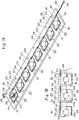
- Unité d'émission de lumière (1) comprenant : un substrat de montage (2) ; et une pluralité d'éléments électroluminescents à semi-conducteurs (3) disposés sur un côté de surface du substrat de montage (2),
dans laquelle le substrat de montage (2) est pourvu d'une plaque de transfert de chaleur (21) qui est constituée d'une première plaque métallique et dans laquelle les éléments électroluminescents à semi-conducteurs (3) sont montés sur un côté de surface de la plaque de transfert de chaleur (21), d'un motif de câblage (22) qui est disposé sur l'autre côté de surface de la plaque de transfert de chaleur (21) et auquel les éléments électroluminescents à semi-conducteurs (3) sont connectés électriquement, et d'une couche isolante (23) interposée entre la plaque de transfert de chaleur (21) et le motif de câblage (22),
dans laquelle les éléments électroluminescents à semi-conducteurs (3) sont des puces de DEL,
caractérisée en ce que
le motif de câblage (22) est constitué d'une deuxième plaque métallique,
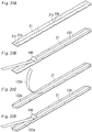
chacune des puces de DEL est pourvue d'une première électrode (31) et d'une deuxième électrode (32) sur un côté de surface de chacune des puces de DEL dans une direction d'épaisseur, la première électrode (31) et la deuxième électrode (32) sont connectées électriquement, par l'intermédiaire de fils de liaison (26), au motif de câblage (22), et la plaque de transfert de chaleur (21) est formée avec des trous traversants (21b) pour le passage des fils de liaison (26) respectifs à travers ceux-ci. - Unité d'émission de lumière (1) selon la revendication 1, dans laquelle la couche isolante (23) comprend une charge dans une résine thermodurcissable, la charge ayant une conductivité thermique supérieure à celle de la résine thermodurcissable.
- Unité d'émission de lumière (1) selon la revendication 1 ou 2, dans laquelle, dans la plaque de transfert de chaleur (21), la première plaque métallique est une plaque d'aluminium, un film d'aluminium avec une pureté supérieure à celle de la plaque d'aluminium est lamifié sur un côté de la plaque d'aluminium qui est opposé à la couche isolante (23), et un film augmentant la réflexion constitué de films diélectriques de deux types qui diffèrent par leur indice de réfraction est lamifié sur le film d'aluminium.
- Unité d'émission de lumière (1) selon l'une des revendications 1 à 3, comprenant une unité de conversion de couleur (37) qui comprend un matériau translucide et un matériau fluorescent qui émet une lumière d'une couleur différente d'une couleur d'émission de la puce de DEL lorsqu'il est excité par la lumière émise à partir de la puce de DEL,
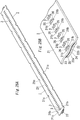
dans laquelle l'unité de conversion de couleur (37) est en contact avec la plaque de transfert de chaleur (21). - Unité d'émission de lumière (1) selon l'une quelconque des revendications 1 à 4, dans laquelle la plaque de transfert de chaleur (21) a une forme allongée, les éléments électroluminescents à semi-conducteurs (3) sont agencés le long d'une direction longitudinale de la plaque de transfert de chaleur (21), et un substrat de base allongé (24) est prévu, lequel a une plus petite différence de coefficient de dilatation linéaire avec la première plaque métallique qu'avec la deuxième plaque métallique, et est disposé sur un côté du motif de câblage (22) qui est opposé à la plaque de transfert de chaleur (21).
- Unité d'émission de lumière (1) selon la revendication 5, dans laquelle le substrat de base (24) est constitué d'un substrat en résine dans lequel une charge est mélangée avec une résine, la charge ayant une conductivité thermique supérieure à celle de la résine.
- Unité d'émission de lumière (1) selon la revendication 5, dans laquelle le substrat de base (24) est constitué d'une troisième plaque métallique constituée du même matériau que celui de la première plaque métallique, et une deuxième couche isolante (25) constituée du même matériau que celui d'une première couche isolante (23), qui est la couche isolante (23), est interposée entre le substrat de base (24) et le motif de câblage (22).
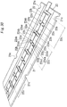
- Unité d'émission de lumière (1) selon l'une quelconque des revendications 1 à 4 comprenant en outre une deuxième plaque de transfert de chaleur (24) constituée d'une première plaque métallique, de sorte qu'une paire de plaques de transfert de chaleur (21) est formée, et les deux plaques de transfert de chaleur (21, 24) sont disposées à distance l'une de l'autre dans une direction d'épaisseur ;
dans laquelle les éléments électroluminescents à semi-conducteurs (3) sont en outre montés sur un côté de surface de la deuxième plaque de transfert de chaleur (24), qui est du côté opposé aux côtés de surface de la paire de plaques de transfert de chaleur (21, 24) qui se font mutuellement face ; et
l'unité d'émission de lumière (1) comprend en outre une deuxième couche isolante (25), qui est interposée entre le motif de câblage (22) et la deuxième plaque de transfert de chaleur (24). - Unité d'émission de lumière (1) selon la revendication 8, dans laquelle les éléments électroluminescents à semi-conducteurs (3) montés sur un côté de surface de la deuxième plaque de transfert de chaleur (24) sont des puces de DEL.
- Unité d'émission de lumière (1) selon la revendication 9, dans laquelle, dans la deuxième plaque de transfert de chaleur (24), la première plaque métallique est une plaque d'aluminium, un film d'aluminium avec une pureté supérieure à celle de la plaque d'aluminium est lamifié sur un côté de la plaque d'aluminium qui est opposé à la deuxième couche isolante (25), et un film augmentant la réflexion constitué de films diélectriques de deux types qui diffèrent par leur indice de réfraction est lamifié sur le film d'aluminium.
- Unité d'émission de lumière (1) selon la revendication 9 ou 10 comprenant une deuxième unité de conversion de couleur (37) qui comprend un matériau translucide et un matériau fluorescent qui émet une lumière d'une couleur différente d'une couleur d'émission d'une puce de DEL correspondante des puces de DEL lorsqu'il est excité par la lumière émise à partir de la puce de DEL correspondante des puces de DEL,
dans laquelle chaque unité de conversion de couleur (37) est en contact avec une plaque de transfert de chaleur correspondante de la paire de plaques de transfert de chaleur (21, 24). - Unité d'émission de lumière (1) selon l'une quelconque des revendications 9 à 11, dans laquelle chacune des puces de DEL est pourvue d'une première électrode (31) et d'une deuxième électrode (32) sur un côté de surface de chacune des puces de DEL dans une direction d'épaisseur, la première électrode (31) et la deuxième électrode (32) sont connectées électriquement, par l'intermédiaire de fils, au motif de câblage (22), et chacune de la paire de plaques de transfert de chaleur (21) est formée avec des trous traversants (21b) pour le passage des fils respectifs à travers ceux-ci.
- Appareil d'éclairage comprenant l'unité d'émission de lumière (1) selon l'une quelconque des revendications 1 à 12.
Applications Claiming Priority (6)
| Application Number | Priority Date | Filing Date | Title |
|---|---|---|---|
| JP2010101182 | 2010-04-26 | ||
| JP2010125097A JP2011249737A (ja) | 2010-04-26 | 2010-05-31 | リードフレーム、配線板およびそれを用いたledユニット |
| JP2011072773A JP5011442B1 (ja) | 2011-03-29 | 2011-03-29 | 発光ユニットおよび照明装置 |
| JP2011072772A JP5011441B1 (ja) | 2011-03-29 | 2011-03-29 | 発光ユニットおよび照明装置 |
| JP2011072774A JP2012209366A (ja) | 2011-03-29 | 2011-03-29 | 両面発光ユニットおよび照明装置 |
| PCT/JP2011/060193 WO2011136236A1 (fr) | 2010-04-26 | 2011-04-26 | Grille de connexion, carte de câblage, unité électroluminescente, et appareil d'éclairage |
Publications (3)
| Publication Number | Publication Date |
|---|---|
| EP2565951A1 EP2565951A1 (fr) | 2013-03-06 |
| EP2565951A4 EP2565951A4 (fr) | 2017-05-03 |
| EP2565951B1 true EP2565951B1 (fr) | 2019-07-31 |
Family
ID=47629989
Family Applications (1)
| Application Number | Title | Priority Date | Filing Date |
|---|---|---|---|
| EP11775017.4A Active EP2565951B1 (fr) | 2010-04-26 | 2011-04-26 | Unité électroluminescente et appareil d'éclairage |
Country Status (5)
| Country | Link |
|---|---|
| US (1) | US8967827B2 (fr) |
| EP (1) | EP2565951B1 (fr) |
| KR (1) | KR101495580B1 (fr) |
| CN (1) | CN102893418B (fr) |
| WO (1) | WO2011136236A1 (fr) |
Families Citing this family (64)
| Publication number | Priority date | Publication date | Assignee | Title |
|---|---|---|---|---|
| US8851356B1 (en) | 2008-02-14 | 2014-10-07 | Metrospec Technology, L.L.C. | Flexible circuit board interconnection and methods |
| US8007286B1 (en) | 2008-03-18 | 2011-08-30 | Metrospec Technology, Llc | Circuit boards interconnected by overlapping plated through holes portions |
| US10334735B2 (en) | 2008-02-14 | 2019-06-25 | Metrospec Technology, L.L.C. | LED lighting systems and methods |
| US8143631B2 (en) | 2008-03-06 | 2012-03-27 | Metrospec Technology Llc | Layered structure for use with high power light emitting diode systems |
| US11266014B2 (en) | 2008-02-14 | 2022-03-01 | Metrospec Technology, L.L.C. | LED lighting systems and method |
| JP5528900B2 (ja) * | 2010-04-30 | 2014-06-25 | ローム株式会社 | 発光素子モジュール |
| DE102011003608A1 (de) * | 2010-08-20 | 2012-02-23 | Tridonic Gmbh & Co. Kg | Gehäustes LED-Modul |
| JP5283195B2 (ja) * | 2010-09-07 | 2013-09-04 | シーシーエス株式会社 | Led配線基板及び光照射装置 |
| JP5049382B2 (ja) * | 2010-12-21 | 2012-10-17 | パナソニック株式会社 | 発光装置及びそれを用いた照明装置 |
| JP2012186450A (ja) * | 2011-02-16 | 2012-09-27 | Rohm Co Ltd | Ledモジュール |
| JP5404705B2 (ja) * | 2011-07-25 | 2014-02-05 | 京セラコネクタプロダクツ株式会社 | 半導体発光素子取付用モジュールの製造方法、及び、半導体発光素子モジュールの製造方法 |
| KR101869554B1 (ko) * | 2011-08-19 | 2018-06-21 | 엘지이노텍 주식회사 | 표시장치 |
| JP5236843B1 (ja) * | 2011-10-11 | 2013-07-17 | パナソニック株式会社 | 発光装置およびこれを用いた照明装置 |
| CN104094426B (zh) * | 2012-02-02 | 2017-09-01 | 西铁城时计株式会社 | 半导体发光装置及其制造方法 |
| US8587099B1 (en) * | 2012-05-02 | 2013-11-19 | Texas Instruments Incorporated | Leadframe having selective planishing |
| JP2014135471A (ja) * | 2012-12-10 | 2014-07-24 | Nitto Denko Corp | 発光装置、発光装置集合体および電極付基板 |
| JP5938623B2 (ja) * | 2012-06-21 | 2016-06-22 | パナソニックIpマネジメント株式会社 | 実装基板およびその製造方法、ledモジュール |
| JP5954657B2 (ja) * | 2012-06-21 | 2016-07-20 | パナソニックIpマネジメント株式会社 | 実装基板およびその製造方法、ledモジュール |
| JP6007249B2 (ja) * | 2012-07-19 | 2016-10-12 | シャープ株式会社 | 列発光装置およびその製造方法 |
| EP2888517A1 (fr) * | 2012-08-22 | 2015-07-01 | Metrospec Technology, L.L.C. | Systèmes et procédés d'éclairage à led |
| JP6209874B2 (ja) * | 2012-08-31 | 2017-10-11 | 日亜化学工業株式会社 | 発光装置及びその製造方法 |
| US9494285B2 (en) | 2013-01-13 | 2016-11-15 | Mag Instrument, Inc | Lighting devices |
| US9748164B2 (en) * | 2013-03-05 | 2017-08-29 | Nichia Corporation | Semiconductor device |
| US10094523B2 (en) * | 2013-04-19 | 2018-10-09 | Cree, Inc. | LED assembly |
| KR102085888B1 (ko) | 2013-05-08 | 2020-03-06 | 엘지이노텍 주식회사 | 발광 소자 |
| TW201500774A (zh) * | 2013-06-25 | 2015-01-01 | Hon Hai Prec Ind Co Ltd | 透鏡及其製作方法 |
| TWI589964B (zh) * | 2013-12-26 | 2017-07-01 | 鴻海精密工業股份有限公司 | 發光裝置及背光模組 |
| CN103872207A (zh) * | 2014-02-21 | 2014-06-18 | 东莞美盛电器制品有限公司 | 一种强光led光源模块及其生产工艺 |
| CH709337B1 (fr) * | 2014-03-04 | 2016-12-30 | Robert Alderton | Unité d'éclairage LED et procédé de fabrication d'une telle unité. |
| CN103968347A (zh) * | 2014-04-04 | 2014-08-06 | 厦门市东林电子有限公司 | 一种led灯的金属散热支架及led光源板和集成散热式led灯 |
| KR102273875B1 (ko) * | 2014-08-01 | 2021-07-05 | 엘지디스플레이 주식회사 | 백라이트부용 led 어레이 및 이의 제조방법 |
| JP6372257B2 (ja) * | 2014-08-29 | 2018-08-15 | 東芝ライテック株式会社 | 車両用発光モジュール、車両用照明装置、および車両用灯具 |
| WO2016106053A1 (fr) | 2014-12-22 | 2016-06-30 | Mag Instrument Inc. | Appareil d'éclairage à efficacité améliorée pourvu d'une del montée directement sur un dissipateur thermique |
| DE102015107657A1 (de) | 2015-05-15 | 2016-12-01 | Alanod Gmbh & Co. Kg | Verfahren zur Herstellung eines Anschlussträgers, Anschlussträger sowie optoelektronisches Halbleiterbauteil mit einem Anschlussträger |
| JP6380314B2 (ja) * | 2015-09-24 | 2018-08-29 | 日亜化学工業株式会社 | 発光装置 |
| WO2017075110A1 (fr) * | 2015-10-26 | 2017-05-04 | Hoffman Jeremy P | Bande linéaire lumineuse à del, structure de montage et ensemble attache |
| JP6728676B2 (ja) * | 2015-12-26 | 2020-07-22 | 日亜化学工業株式会社 | 発光装置 |
| US10381294B2 (en) * | 2016-02-01 | 2019-08-13 | Advanced Semiconductor Engineering, Inc. | Semiconductor package device |
| US20170328544A1 (en) * | 2016-05-16 | 2017-11-16 | GE Lighting Solutions, LLC | Snap-in assembling of led boards in luminaires |
| JP6720747B2 (ja) | 2016-07-19 | 2020-07-08 | 日亜化学工業株式会社 | 半導体装置、基台及びそれらの製造方法 |
| CN205863332U (zh) * | 2016-07-29 | 2017-01-04 | 泰科电子(上海)有限公司 | 测温组件、电器组件、电池包连接组件及汽车电池包 |
| JP6246879B1 (ja) | 2016-09-20 | 2017-12-13 | 株式会社東芝 | 光半導体モジュール及びその製造方法 |
| JP7320452B2 (ja) * | 2017-03-21 | 2023-08-03 | ルミレッズ ホールディング ベーフェー | 平坦なキャリア上へのled素子の取り付け |
| US10260683B2 (en) | 2017-05-10 | 2019-04-16 | Cree, Inc. | Solid-state lamp with LED filaments having different CCT's |
| TW201901894A (zh) * | 2017-05-18 | 2019-01-01 | 復盛精密工業股份有限公司 | 具線路之導線架的製作方法及其結構 |
| JP6680274B2 (ja) * | 2017-06-27 | 2020-04-15 | 日亜化学工業株式会社 | 発光装置及び樹脂付リードフレーム |
| DE102017126044A1 (de) * | 2017-11-08 | 2019-05-09 | HELLA GmbH & Co. KGaA | Schaltungsanordnung einer Leuchteinheit eines Scheinwerfers für ein Fahrzeug |
| JP6958274B2 (ja) * | 2017-11-16 | 2021-11-02 | 富士電機株式会社 | 電力用半導体装置 |
| CN110020578A (zh) | 2018-01-10 | 2019-07-16 | 广东欧珀移动通信有限公司 | 图像处理方法、装置、存储介质及电子设备 |
| US20190267526A1 (en) | 2018-02-26 | 2019-08-29 | Semicon Light Co., Ltd. | Semiconductor Light Emitting Devices And Method Of Manufacturing The Same |
| US10775851B2 (en) * | 2018-03-30 | 2020-09-15 | Sara Stewart | Memory aid |
| CN110504244A (zh) * | 2018-05-18 | 2019-11-26 | 深圳市聚飞光电股份有限公司 | Led及发光装置 |
| JP7197765B2 (ja) * | 2018-08-03 | 2022-12-28 | 日亜化学工業株式会社 | 発光装置 |
| US10566513B1 (en) * | 2018-09-17 | 2020-02-18 | Chieh-Chen Tseng | LED circuit structure |
| US10849200B2 (en) | 2018-09-28 | 2020-11-24 | Metrospec Technology, L.L.C. | Solid state lighting circuit with current bias and method of controlling thereof |
| DE102018124471B3 (de) * | 2018-10-04 | 2019-12-05 | Ledvance Gmbh | Verfahren zum Herstellen eines Leadframes für eine Röhrenlampe, Leadframe und Röhrenlampe |
| US10801679B2 (en) * | 2018-10-08 | 2020-10-13 | RAB Lighting Inc. | Apparatuses and methods for assembling luminaires |
| TWI688308B (zh) * | 2018-10-12 | 2020-03-11 | 聯嘉光電股份有限公司 | 均勻發光之led線形光源元件及其方法 |
| US11032976B1 (en) | 2020-03-16 | 2021-06-15 | Hgci, Inc. | Light fixture for indoor grow application and components thereof |
| USD933872S1 (en) | 2020-03-16 | 2021-10-19 | Hgci, Inc. | Light fixture |
| USD933881S1 (en) | 2020-03-16 | 2021-10-19 | Hgci, Inc. | Light fixture having heat sink |
| CN114286513B (zh) * | 2021-11-30 | 2024-02-06 | 通元科技(惠州)有限公司 | 一种非对称预应力消除型led背板及其制作方法 |
| US11729915B1 (en) * | 2022-03-22 | 2023-08-15 | Tactotek Oy | Method for manufacturing a number of electrical nodes, electrical node module, electrical node, and multilayer structure |
| CN116772131A (zh) * | 2023-06-26 | 2023-09-19 | 惠科股份有限公司 | 灯板、灯板的制备方法及显示装置 |
Family Cites Families (33)
| Publication number | Priority date | Publication date | Assignee | Title |
|---|---|---|---|---|
| US5660461A (en) | 1994-12-08 | 1997-08-26 | Quantum Devices, Inc. | Arrays of optoelectronic devices and method of making same |
| JP3627478B2 (ja) | 1997-11-25 | 2005-03-09 | 松下電工株式会社 | 光源装置 |
| US6548832B1 (en) | 1999-06-09 | 2003-04-15 | Sanyo Electric Co., Ltd. | Hybrid integrated circuit device |
| JP2001068742A (ja) | 1999-08-25 | 2001-03-16 | Sanyo Electric Co Ltd | 混成集積回路装置 |
| JP2000353826A (ja) * | 1999-06-09 | 2000-12-19 | Sanyo Electric Co Ltd | 混成集積回路装置および光照射装置 |
| US6489637B1 (en) | 1999-06-09 | 2002-12-03 | Sanyo Electric Co., Ltd. | Hybrid integrated circuit device |
| JP4412787B2 (ja) * | 1999-06-09 | 2010-02-10 | 三洋電機株式会社 | 金属基板を採用した照射装置および照射モジュール |
| JP4190095B2 (ja) | 1999-07-29 | 2008-12-03 | 三洋電機株式会社 | 混成集積回路装置 |
| JP3696020B2 (ja) * | 2000-01-20 | 2005-09-14 | 三洋電機株式会社 | 混成集積回路装置 |
| TW567619B (en) * | 2001-08-09 | 2003-12-21 | Matsushita Electric Ind Co Ltd | LED lighting apparatus and card-type LED light source |
| US20080043444A1 (en) | 2004-04-27 | 2008-02-21 | Kyocera Corporation | Wiring Board for Light-Emitting Element |
| JP2006147999A (ja) | 2004-11-24 | 2006-06-08 | Kyocera Corp | 発光素子用配線基板並びに発光装置 |
| JP2006066631A (ja) | 2004-08-26 | 2006-03-09 | Kyocera Corp | 配線基板および電気装置並びに発光装置 |
| JP2006093470A (ja) | 2004-09-24 | 2006-04-06 | Toshiba Corp | リードフレーム、発光装置、発光装置の製造方法 |
| KR100631901B1 (ko) * | 2005-01-31 | 2006-10-11 | 삼성전기주식회사 | Led 패키지 프레임 및 이를 채용하는 led 패키지 |
| KR100610650B1 (ko) * | 2005-06-17 | 2006-08-09 | (주) 파이오닉스 | 엘이디 패키지 및 그 제조방법 |
| JP4810913B2 (ja) | 2005-07-26 | 2011-11-09 | パナソニック電工株式会社 | 光源装置、及びそれを用いた照明器具 |
| JP2007258619A (ja) | 2006-03-24 | 2007-10-04 | Ngk Spark Plug Co Ltd | 発光素子収納用パッケージ |
| US8779444B2 (en) * | 2006-11-03 | 2014-07-15 | Relume Technologies, Inc. | LED light engine with applied foil construction |
| JP4245041B2 (ja) * | 2006-11-27 | 2009-03-25 | セイコーエプソン株式会社 | 照明装置及びプロジェクタ |
| EP1928026A1 (fr) * | 2006-11-30 | 2008-06-04 | Toshiba Lighting & Technology Corporation | Dispositif d'éclairage doté d'éléments luminescents semi-conducteurs |
| JPWO2008078791A1 (ja) | 2006-12-27 | 2010-04-30 | 昭和電工株式会社 | 発光装置の製造方法 |
| KR100802393B1 (ko) * | 2007-02-15 | 2008-02-13 | 삼성전기주식회사 | 패키지 기판 및 그 제조방법 |
| US7938558B2 (en) * | 2007-05-04 | 2011-05-10 | Ruud Lighting, Inc. | Safety accommodation arrangement in LED package/lens structure |
| JP4888280B2 (ja) | 2007-08-28 | 2012-02-29 | パナソニック電工株式会社 | 発光装置 |
| JP5538671B2 (ja) | 2007-09-19 | 2014-07-02 | シャープ株式会社 | 発光装置およびledランプ |
| JP2009105379A (ja) | 2007-10-05 | 2009-05-14 | Panasonic Electric Works Co Ltd | 発光装置 |
| JP5149601B2 (ja) * | 2007-11-27 | 2013-02-20 | パナソニック株式会社 | 発光装置 |
| JP2009130300A (ja) | 2007-11-27 | 2009-06-11 | Panasonic Electric Works Co Ltd | 発光装置の製造方法 |
| TW200923262A (en) * | 2007-11-30 | 2009-06-01 | Tysun Inc | High heat dissipation optic module for light emitting diode and its manufacturing method |
| EP2256830B1 (fr) | 2008-03-26 | 2019-05-01 | Shimane Prefectural Government | Module électroluminescent à semi-conducteur et dispositif électroluminescent à semi-conducteur |
| JP4627088B2 (ja) | 2008-04-22 | 2011-02-09 | 明和ベンディクス株式会社 | Led発光体を内蔵してなる照明装置 |
| US7973332B2 (en) * | 2008-05-26 | 2011-07-05 | Rohm Co., Ltd. | Lamp and method of making the same |
-
2011
- 2011-04-26 CN CN201180020874.8A patent/CN102893418B/zh not_active Expired - Fee Related
- 2011-04-26 WO PCT/JP2011/060193 patent/WO2011136236A1/fr active Application Filing
- 2011-04-26 US US13/641,483 patent/US8967827B2/en not_active Expired - Fee Related
- 2011-04-26 KR KR1020127026385A patent/KR101495580B1/ko active IP Right Grant
- 2011-04-26 EP EP11775017.4A patent/EP2565951B1/fr active Active
Non-Patent Citations (1)
| Title |
|---|
| None * |
Also Published As
| Publication number | Publication date |
|---|---|
| EP2565951A1 (fr) | 2013-03-06 |
| WO2011136236A1 (fr) | 2011-11-03 |
| KR101495580B1 (ko) | 2015-02-25 |
| US8967827B2 (en) | 2015-03-03 |
| CN102893418A (zh) | 2013-01-23 |
| EP2565951A4 (fr) | 2017-05-03 |
| KR20120123601A (ko) | 2012-11-08 |
| CN102893418B (zh) | 2015-07-22 |
| US20130070452A1 (en) | 2013-03-21 |
Similar Documents
| Publication | Publication Date | Title |
|---|---|---|
| EP2565951B1 (fr) | Unité électroluminescente et appareil d'éclairage | |
| EP2469613B1 (fr) | Dispositif électroluminescent et appareil d'éclairage l'utilisant | |
| KR101182742B1 (ko) | 반도체 발광모듈 및 그 제조방법 | |
| EP2363884B1 (fr) | Ensemble d'éclairage et dispositif d'affichage le comprenant | |
| US8592830B2 (en) | LED unit | |
| US20050045903A1 (en) | Surface-mounted light-emitting diode and method | |
| US9196584B2 (en) | Light-emitting device and lighting apparatus using the same | |
| KR20080059224A (ko) | Led조명 기구 | |
| JP2011249737A (ja) | リードフレーム、配線板およびそれを用いたledユニット | |
| KR101051488B1 (ko) | 발광 다이오드 유닛의 제조 방법과, 이 방법에 의하여 제조된 발광 다이오드 유닛 | |
| EP2478750B1 (fr) | Module d'éclairage et dispositif électroluminescent | |
| US20130250562A1 (en) | Wiring board device, luminaire, and manufacturing method of the wiring board device | |
| US20120256205A1 (en) | Led lighting module with uniform light output | |
| KR100985917B1 (ko) | 대전력 광원 램프를 위한 효과적인 열방출 구조의 리드프레임, 전자 소자 및 그 제조 방법 | |
| JP5011442B1 (ja) | 発光ユニットおよび照明装置 | |
| KR100638881B1 (ko) | 금속 기판에 led 패키지를 삽입한 led 어셈블리 | |
| JP2009283385A (ja) | 照明装置 | |
| JP2013093409A (ja) | リードフレーム、配線板およびそれを用いたledユニット | |
| KR20110070520A (ko) | 발광소자 패키지 및 그 제조방법 |
Legal Events
| Date | Code | Title | Description |
|---|---|---|---|
| PUAI | Public reference made under article 153(3) epc to a published international application that has entered the european phase |
Free format text: ORIGINAL CODE: 0009012 |
|
| 17P | Request for examination filed |
Effective date: 20121019 |
|
| AK | Designated contracting states |
Kind code of ref document: A1 Designated state(s): AL AT BE BG CH CY CZ DE DK EE ES FI FR GB GR HR HU IE IS IT LI LT LU LV MC MK MT NL NO PL PT RO RS SE SI SK SM TR |
|
| DAX | Request for extension of the european patent (deleted) | ||
| RAP1 | Party data changed (applicant data changed or rights of an application transferred) |
Owner name: PANASONIC INTELLECTUAL PROPERTY MANAGEMENT CO., LT |
|
| RA4 | Supplementary search report drawn up and despatched (corrected) |
Effective date: 20170330 |
|
| RIC1 | Information provided on ipc code assigned before grant |
Ipc: H01L 23/00 20060101ALI20170325BHEP Ipc: F21K 9/20 20160101ALI20170325BHEP Ipc: F21Y 103/10 20160101ALN20170325BHEP Ipc: H05K 1/18 20060101ALI20170325BHEP Ipc: F21K 9/27 20160101ALI20170325BHEP Ipc: H01L 33/62 20100101ALI20170325BHEP Ipc: H05K 1/05 20060101ALN20170325BHEP Ipc: H01L 25/075 20060101ALN20170325BHEP Ipc: F21V 19/00 20060101ALI20170325BHEP Ipc: H05K 3/20 20060101ALN20170325BHEP Ipc: H01L 33/64 20100101ALI20170325BHEP Ipc: F21Y 115/10 20160101ALN20170325BHEP Ipc: F21Y 107/90 20160101ALN20170325BHEP Ipc: F21Y 105/10 20160101ALN20170325BHEP Ipc: F21K 9/90 20160101ALI20170325BHEP Ipc: H05K 1/02 20060101AFI20170325BHEP Ipc: H01L 33/48 20100101ALN20170325BHEP |
|
| RIC1 | Information provided on ipc code assigned before grant |
Ipc: H01L 33/62 20100101ALI20180920BHEP Ipc: F21K 9/27 20160101ALI20180920BHEP Ipc: F21K 9/20 20160101ALI20180920BHEP Ipc: H05K 3/20 20060101ALN20180920BHEP Ipc: H01L 33/64 20100101ALI20180920BHEP Ipc: F21Y 115/10 20160101ALN20180920BHEP Ipc: F21V 19/00 20060101ALI20180920BHEP Ipc: H01L 33/48 20100101ALN20180920BHEP Ipc: H05K 1/18 20060101ALI20180920BHEP Ipc: F21Y 103/10 20160101ALN20180920BHEP Ipc: F21Y 107/90 20160101ALN20180920BHEP Ipc: H05K 1/05 20060101ALN20180920BHEP Ipc: F21K 9/90 20160101ALI20180920BHEP Ipc: H05K 1/02 20060101AFI20180920BHEP Ipc: H01L 25/075 20060101ALN20180920BHEP Ipc: H01L 23/00 20060101ALI20180920BHEP Ipc: F21Y 105/10 20160101ALN20180920BHEP |
|
| GRAP | Despatch of communication of intention to grant a patent |
Free format text: ORIGINAL CODE: EPIDOSNIGR1 |
|
| STAA | Information on the status of an ep patent application or granted ep patent |
Free format text: STATUS: GRANT OF PATENT IS INTENDED |
|
| RIC1 | Information provided on ipc code assigned before grant |
Ipc: H01L 33/48 20100101ALN20181011BHEP Ipc: F21Y 115/10 20130306ALN20181011BHEP Ipc: H01L 33/62 20100101ALI20181011BHEP Ipc: H05K 3/20 20060101ALN20181011BHEP Ipc: H01L 25/075 20060101ALN20181011BHEP Ipc: F21K 9/20 20130306ALI20181011BHEP Ipc: F21Y 103/10 20130306ALN20181011BHEP Ipc: H05K 1/02 20060101AFI20181011BHEP Ipc: H01L 33/64 20100101ALI20181011BHEP Ipc: F21Y 105/10 20130306ALN20181011BHEP Ipc: F21V 19/00 20060101ALI20181011BHEP Ipc: F21K 9/90 20130306ALI20181011BHEP Ipc: F21Y 107/90 20130306ALN20181011BHEP Ipc: H01L 23/00 20060101ALI20181011BHEP Ipc: H05K 1/18 20060101ALI20181011BHEP Ipc: F21K 9/27 20130306ALI20181011BHEP Ipc: H05K 1/05 20060101ALN20181011BHEP |
|
| INTG | Intention to grant announced |
Effective date: 20181030 |
|
| RIN1 | Information on inventor provided before grant (corrected) |
Inventor name: TANAKA, KENICHIRO Inventor name: KUZUHARA, IKKO Inventor name: URANO, YOJI Inventor name: YOKOTANI, RYOJI |
|
| RIC1 | Information provided on ipc code assigned before grant |
Ipc: F21Y 103/10 20160101ALN20181011BHEP Ipc: H05K 1/05 20060101ALN20181011BHEP Ipc: F21K 9/90 20160101ALI20181011BHEP Ipc: F21V 19/00 20060101ALI20181011BHEP Ipc: F21K 9/20 20160101ALI20181011BHEP Ipc: H01L 33/62 20100101ALI20181011BHEP Ipc: F21Y 105/10 20160101ALN20181011BHEP Ipc: H05K 3/20 20060101ALN20181011BHEP Ipc: F21Y 115/10 20160101ALN20181011BHEP Ipc: F21Y 107/90 20160101ALN20181011BHEP Ipc: H01L 33/48 20100101ALN20181011BHEP Ipc: H05K 1/18 20060101ALI20181011BHEP Ipc: H05K 1/02 20060101AFI20181011BHEP Ipc: H01L 33/64 20100101ALI20181011BHEP Ipc: H01L 23/00 20060101ALI20181011BHEP Ipc: F21K 9/27 20160101ALI20181011BHEP Ipc: H01L 25/075 20060101ALN20181011BHEP |
|
| RIC1 | Information provided on ipc code assigned before grant |
Ipc: F21Y 105/10 20160101ALN20181011BHEP Ipc: F21Y 115/10 20160101ALN20181011BHEP Ipc: F21V 19/00 20060101ALI20181011BHEP Ipc: F21K 9/20 20160101ALI20181011BHEP Ipc: F21Y 103/10 20160101ALN20181011BHEP Ipc: H05K 1/05 20060101ALN20181011BHEP Ipc: F21K 9/90 20160101ALI20181011BHEP Ipc: H01L 33/62 20100101ALI20181011BHEP Ipc: H01L 33/64 20100101ALI20181011BHEP Ipc: H05K 3/20 20060101ALN20181011BHEP Ipc: F21Y 107/90 20160101ALN20181011BHEP Ipc: H01L 23/00 20060101ALI20181011BHEP Ipc: H05K 1/02 20060101AFI20181011BHEP Ipc: H01L 25/075 20060101ALN20181011BHEP Ipc: F21K 9/27 20160101ALI20181011BHEP Ipc: H05K 1/18 20060101ALI20181011BHEP Ipc: H01L 33/48 20100101ALN20181011BHEP |
|
| GRAJ | Information related to disapproval of communication of intention to grant by the applicant or resumption of examination proceedings by the epo deleted |
Free format text: ORIGINAL CODE: EPIDOSDIGR1 |
|
| STAA | Information on the status of an ep patent application or granted ep patent |
Free format text: STATUS: REQUEST FOR EXAMINATION WAS MADE |
|
| REG | Reference to a national code |
Ref country code: DE Ref legal event code: R079 Ref document number: 602011060894 Country of ref document: DE Free format text: PREVIOUS MAIN CLASS: H01L0033620000 Ipc: H05K0001020000 |
|
| GRAP | Despatch of communication of intention to grant a patent |
Free format text: ORIGINAL CODE: EPIDOSNIGR1 |
|
| STAA | Information on the status of an ep patent application or granted ep patent |
Free format text: STATUS: GRANT OF PATENT IS INTENDED |
|
| INTC | Intention to grant announced (deleted) | ||
| RIC1 | Information provided on ipc code assigned before grant |
Ipc: H01L 33/64 20100101ALI20190221BHEP Ipc: H01L 33/62 20100101ALI20190221BHEP Ipc: F21K 9/20 20160101ALI20190221BHEP Ipc: F21K 9/27 20160101ALI20190221BHEP Ipc: H01L 23/00 20060101ALI20190221BHEP Ipc: H01L 25/075 20060101ALN20190221BHEP Ipc: H01L 33/48 20100101ALN20190221BHEP Ipc: F21Y 115/10 20160101ALN20190221BHEP Ipc: F21Y 105/10 20160101ALN20190221BHEP Ipc: H05K 3/20 20060101ALN20190221BHEP Ipc: F21K 9/90 20160101ALI20190221BHEP Ipc: F21Y 107/90 20160101ALN20190221BHEP Ipc: H05K 1/05 20060101ALN20190221BHEP Ipc: F21V 19/00 20060101ALI20190221BHEP Ipc: F21Y 103/10 20160101ALN20190221BHEP Ipc: H05K 1/18 20060101ALI20190221BHEP Ipc: H05K 1/02 20060101AFI20190221BHEP |
|
| INTG | Intention to grant announced |
Effective date: 20190305 |
|
| GRAS | Grant fee paid |
Free format text: ORIGINAL CODE: EPIDOSNIGR3 |
|
| GRAA | (expected) grant |
Free format text: ORIGINAL CODE: 0009210 |
|
| STAA | Information on the status of an ep patent application or granted ep patent |
Free format text: STATUS: THE PATENT HAS BEEN GRANTED |
|
| AK | Designated contracting states |
Kind code of ref document: B1 Designated state(s): AL AT BE BG CH CY CZ DE DK EE ES FI FR GB GR HR HU IE IS IT LI LT LU LV MC MK MT NL NO PL PT RO RS SE SI SK SM TR |
|
| REG | Reference to a national code |
Ref country code: CH Ref legal event code: EP Ref country code: GB Ref legal event code: FG4D |
|
| REG | Reference to a national code |
Ref country code: AT Ref legal event code: REF Ref document number: 1162400 Country of ref document: AT Kind code of ref document: T Effective date: 20190815 |
|
| REG | Reference to a national code |
Ref country code: IE Ref legal event code: FG4D |
|
| REG | Reference to a national code |
Ref country code: DE Ref legal event code: R096 Ref document number: 602011060894 Country of ref document: DE |
|
| REG | Reference to a national code |
Ref country code: NL Ref legal event code: MP Effective date: 20190731 |
|
| REG | Reference to a national code |
Ref country code: LT Ref legal event code: MG4D |
|
| REG | Reference to a national code |
Ref country code: AT Ref legal event code: MK05 Ref document number: 1162400 Country of ref document: AT Kind code of ref document: T Effective date: 20190731 |
|
| PG25 | Lapsed in a contracting state [announced via postgrant information from national office to epo] |
Ref country code: FI Free format text: LAPSE BECAUSE OF FAILURE TO SUBMIT A TRANSLATION OF THE DESCRIPTION OR TO PAY THE FEE WITHIN THE PRESCRIBED TIME-LIMIT Effective date: 20190731 Ref country code: BG Free format text: LAPSE BECAUSE OF FAILURE TO SUBMIT A TRANSLATION OF THE DESCRIPTION OR TO PAY THE FEE WITHIN THE PRESCRIBED TIME-LIMIT Effective date: 20191031 Ref country code: NO Free format text: LAPSE BECAUSE OF FAILURE TO SUBMIT A TRANSLATION OF THE DESCRIPTION OR TO PAY THE FEE WITHIN THE PRESCRIBED TIME-LIMIT Effective date: 20191031 Ref country code: SE Free format text: LAPSE BECAUSE OF FAILURE TO SUBMIT A TRANSLATION OF THE DESCRIPTION OR TO PAY THE FEE WITHIN THE PRESCRIBED TIME-LIMIT Effective date: 20190731 Ref country code: AT Free format text: LAPSE BECAUSE OF FAILURE TO SUBMIT A TRANSLATION OF THE DESCRIPTION OR TO PAY THE FEE WITHIN THE PRESCRIBED TIME-LIMIT Effective date: 20190731 Ref country code: HR Free format text: LAPSE BECAUSE OF FAILURE TO SUBMIT A TRANSLATION OF THE DESCRIPTION OR TO PAY THE FEE WITHIN THE PRESCRIBED TIME-LIMIT Effective date: 20190731 Ref country code: PT Free format text: LAPSE BECAUSE OF FAILURE TO SUBMIT A TRANSLATION OF THE DESCRIPTION OR TO PAY THE FEE WITHIN THE PRESCRIBED TIME-LIMIT Effective date: 20191202 Ref country code: NL Free format text: LAPSE BECAUSE OF FAILURE TO SUBMIT A TRANSLATION OF THE DESCRIPTION OR TO PAY THE FEE WITHIN THE PRESCRIBED TIME-LIMIT Effective date: 20190731 Ref country code: LT Free format text: LAPSE BECAUSE OF FAILURE TO SUBMIT A TRANSLATION OF THE DESCRIPTION OR TO PAY THE FEE WITHIN THE PRESCRIBED TIME-LIMIT Effective date: 20190731 |
|
| PG25 | Lapsed in a contracting state [announced via postgrant information from national office to epo] |
Ref country code: RS Free format text: LAPSE BECAUSE OF FAILURE TO SUBMIT A TRANSLATION OF THE DESCRIPTION OR TO PAY THE FEE WITHIN THE PRESCRIBED TIME-LIMIT Effective date: 20190731 Ref country code: IS Free format text: LAPSE BECAUSE OF FAILURE TO SUBMIT A TRANSLATION OF THE DESCRIPTION OR TO PAY THE FEE WITHIN THE PRESCRIBED TIME-LIMIT Effective date: 20191130 Ref country code: LV Free format text: LAPSE BECAUSE OF FAILURE TO SUBMIT A TRANSLATION OF THE DESCRIPTION OR TO PAY THE FEE WITHIN THE PRESCRIBED TIME-LIMIT Effective date: 20190731 Ref country code: ES Free format text: LAPSE BECAUSE OF FAILURE TO SUBMIT A TRANSLATION OF THE DESCRIPTION OR TO PAY THE FEE WITHIN THE PRESCRIBED TIME-LIMIT Effective date: 20190731 Ref country code: AL Free format text: LAPSE BECAUSE OF FAILURE TO SUBMIT A TRANSLATION OF THE DESCRIPTION OR TO PAY THE FEE WITHIN THE PRESCRIBED TIME-LIMIT Effective date: 20190731 Ref country code: GR Free format text: LAPSE BECAUSE OF FAILURE TO SUBMIT A TRANSLATION OF THE DESCRIPTION OR TO PAY THE FEE WITHIN THE PRESCRIBED TIME-LIMIT Effective date: 20191101 |
|
| PG25 | Lapsed in a contracting state [announced via postgrant information from national office to epo] |
Ref country code: TR Free format text: LAPSE BECAUSE OF FAILURE TO SUBMIT A TRANSLATION OF THE DESCRIPTION OR TO PAY THE FEE WITHIN THE PRESCRIBED TIME-LIMIT Effective date: 20190731 |
|
| PG25 | Lapsed in a contracting state [announced via postgrant information from national office to epo] |
Ref country code: PL Free format text: LAPSE BECAUSE OF FAILURE TO SUBMIT A TRANSLATION OF THE DESCRIPTION OR TO PAY THE FEE WITHIN THE PRESCRIBED TIME-LIMIT Effective date: 20190731 Ref country code: IT Free format text: LAPSE BECAUSE OF FAILURE TO SUBMIT A TRANSLATION OF THE DESCRIPTION OR TO PAY THE FEE WITHIN THE PRESCRIBED TIME-LIMIT Effective date: 20190731 Ref country code: RO Free format text: LAPSE BECAUSE OF FAILURE TO SUBMIT A TRANSLATION OF THE DESCRIPTION OR TO PAY THE FEE WITHIN THE PRESCRIBED TIME-LIMIT Effective date: 20190731 Ref country code: DK Free format text: LAPSE BECAUSE OF FAILURE TO SUBMIT A TRANSLATION OF THE DESCRIPTION OR TO PAY THE FEE WITHIN THE PRESCRIBED TIME-LIMIT Effective date: 20190731 Ref country code: EE Free format text: LAPSE BECAUSE OF FAILURE TO SUBMIT A TRANSLATION OF THE DESCRIPTION OR TO PAY THE FEE WITHIN THE PRESCRIBED TIME-LIMIT Effective date: 20190731 |
|
| PG25 | Lapsed in a contracting state [announced via postgrant information from national office to epo] |
Ref country code: SM Free format text: LAPSE BECAUSE OF FAILURE TO SUBMIT A TRANSLATION OF THE DESCRIPTION OR TO PAY THE FEE WITHIN THE PRESCRIBED TIME-LIMIT Effective date: 20190731 Ref country code: CZ Free format text: LAPSE BECAUSE OF FAILURE TO SUBMIT A TRANSLATION OF THE DESCRIPTION OR TO PAY THE FEE WITHIN THE PRESCRIBED TIME-LIMIT Effective date: 20190731 Ref country code: IS Free format text: LAPSE BECAUSE OF FAILURE TO SUBMIT A TRANSLATION OF THE DESCRIPTION OR TO PAY THE FEE WITHIN THE PRESCRIBED TIME-LIMIT Effective date: 20200224 Ref country code: SK Free format text: LAPSE BECAUSE OF FAILURE TO SUBMIT A TRANSLATION OF THE DESCRIPTION OR TO PAY THE FEE WITHIN THE PRESCRIBED TIME-LIMIT Effective date: 20190731 |
|
| REG | Reference to a national code |
Ref country code: DE Ref legal event code: R097 Ref document number: 602011060894 Country of ref document: DE |
|
| PLBE | No opposition filed within time limit |
Free format text: ORIGINAL CODE: 0009261 |
|
| STAA | Information on the status of an ep patent application or granted ep patent |
Free format text: STATUS: NO OPPOSITION FILED WITHIN TIME LIMIT |
|
| PG2D | Information on lapse in contracting state deleted |
Ref country code: IS |
|
| PG25 | Lapsed in a contracting state [announced via postgrant information from national office to epo] |
Ref country code: IS Free format text: LAPSE BECAUSE OF FAILURE TO SUBMIT A TRANSLATION OF THE DESCRIPTION OR TO PAY THE FEE WITHIN THE PRESCRIBED TIME-LIMIT Effective date: 20191030 |
|
| 26N | No opposition filed |
Effective date: 20200603 |
|
| PG25 | Lapsed in a contracting state [announced via postgrant information from national office to epo] |
Ref country code: SI Free format text: LAPSE BECAUSE OF FAILURE TO SUBMIT A TRANSLATION OF THE DESCRIPTION OR TO PAY THE FEE WITHIN THE PRESCRIBED TIME-LIMIT Effective date: 20190731 |
|
| REG | Reference to a national code |
Ref country code: DE Ref legal event code: R119 Ref document number: 602011060894 Country of ref document: DE |
|
| PG25 | Lapsed in a contracting state [announced via postgrant information from national office to epo] |
Ref country code: MC Free format text: LAPSE BECAUSE OF FAILURE TO SUBMIT A TRANSLATION OF THE DESCRIPTION OR TO PAY THE FEE WITHIN THE PRESCRIBED TIME-LIMIT Effective date: 20190731 |
|
| REG | Reference to a national code |
Ref country code: CH Ref legal event code: PL |
|
| PG25 | Lapsed in a contracting state [announced via postgrant information from national office to epo] |
Ref country code: FR Free format text: LAPSE BECAUSE OF NON-PAYMENT OF DUE FEES Effective date: 20200430 Ref country code: CH Free format text: LAPSE BECAUSE OF NON-PAYMENT OF DUE FEES Effective date: 20200430 Ref country code: LU Free format text: LAPSE BECAUSE OF NON-PAYMENT OF DUE FEES Effective date: 20200426 Ref country code: DE Free format text: LAPSE BECAUSE OF NON-PAYMENT OF DUE FEES Effective date: 20201103 Ref country code: LI Free format text: LAPSE BECAUSE OF NON-PAYMENT OF DUE FEES Effective date: 20200430 |
|
| REG | Reference to a national code |
Ref country code: BE Ref legal event code: MM Effective date: 20200430 |
|
| PG25 | Lapsed in a contracting state [announced via postgrant information from national office to epo] |
Ref country code: BE Free format text: LAPSE BECAUSE OF NON-PAYMENT OF DUE FEES Effective date: 20200430 |
|
| GBPC | Gb: european patent ceased through non-payment of renewal fee |
Effective date: 20200426 |
|
| PG25 | Lapsed in a contracting state [announced via postgrant information from national office to epo] |
Ref country code: GB Free format text: LAPSE BECAUSE OF NON-PAYMENT OF DUE FEES Effective date: 20200426 Ref country code: IE Free format text: LAPSE BECAUSE OF NON-PAYMENT OF DUE FEES Effective date: 20200426 |
|
| PG25 | Lapsed in a contracting state [announced via postgrant information from national office to epo] |
Ref country code: MT Free format text: LAPSE BECAUSE OF FAILURE TO SUBMIT A TRANSLATION OF THE DESCRIPTION OR TO PAY THE FEE WITHIN THE PRESCRIBED TIME-LIMIT Effective date: 20190731 Ref country code: CY Free format text: LAPSE BECAUSE OF FAILURE TO SUBMIT A TRANSLATION OF THE DESCRIPTION OR TO PAY THE FEE WITHIN THE PRESCRIBED TIME-LIMIT Effective date: 20190731 |
|
| PG25 | Lapsed in a contracting state [announced via postgrant information from national office to epo] |
Ref country code: MK Free format text: LAPSE BECAUSE OF FAILURE TO SUBMIT A TRANSLATION OF THE DESCRIPTION OR TO PAY THE FEE WITHIN THE PRESCRIBED TIME-LIMIT Effective date: 20190731 |