EP2426720A1 - Versetzter Dünnfilmtransistor und Herstellungsverfahren dafür - Google Patents
Versetzter Dünnfilmtransistor und Herstellungsverfahren dafür Download PDFInfo
- Publication number
- EP2426720A1 EP2426720A1 EP10175294A EP10175294A EP2426720A1 EP 2426720 A1 EP2426720 A1 EP 2426720A1 EP 10175294 A EP10175294 A EP 10175294A EP 10175294 A EP10175294 A EP 10175294A EP 2426720 A1 EP2426720 A1 EP 2426720A1
- Authority
- EP
- European Patent Office
- Prior art keywords
- layer
- copper
- thin film
- film transistor
- oxide
- Prior art date
- Legal status (The legal status is an assumption and is not a legal conclusion. Google has not performed a legal analysis and makes no representation as to the accuracy of the status listed.)
- Withdrawn
Links
- 239000010409 thin film Substances 0.000 title claims abstract description 53
- 238000000034 method Methods 0.000 title claims abstract description 41
- 229910052802 copper Inorganic materials 0.000 claims abstract description 138
- 239000010949 copper Substances 0.000 claims abstract description 138
- RYGMFSIKBFXOCR-UHFFFAOYSA-N Copper Chemical compound [Cu] RYGMFSIKBFXOCR-UHFFFAOYSA-N 0.000 claims abstract description 134
- 229910000881 Cu alloy Inorganic materials 0.000 claims abstract description 87
- 229910052760 oxygen Inorganic materials 0.000 claims description 44
- QVGXLLKOCUKJST-UHFFFAOYSA-N atomic oxygen Chemical compound [O] QVGXLLKOCUKJST-UHFFFAOYSA-N 0.000 claims description 43
- 239000001301 oxygen Substances 0.000 claims description 43
- 239000000758 substrate Substances 0.000 claims description 35
- 238000004544 sputter deposition Methods 0.000 claims description 27
- 238000000137 annealing Methods 0.000 claims description 26
- 238000000151 deposition Methods 0.000 claims description 26
- 239000000463 material Substances 0.000 claims description 22
- 238000001755 magnetron sputter deposition Methods 0.000 claims description 15
- 238000005275 alloying Methods 0.000 claims description 10
- 238000001465 metallisation Methods 0.000 claims description 10
- 229910052804 chromium Inorganic materials 0.000 claims description 9
- 239000007789 gas Substances 0.000 claims description 9
- 229910052749 magnesium Inorganic materials 0.000 claims description 7
- 229910052748 manganese Inorganic materials 0.000 claims description 7
- 239000000956 alloy Substances 0.000 claims description 6
- 239000011261 inert gas Substances 0.000 claims description 4
- 239000000203 mixture Substances 0.000 claims description 4
- 230000001590 oxidative effect Effects 0.000 claims description 2
- XLOMVQKBTHCTTD-UHFFFAOYSA-N Zinc monoxide Chemical compound [Zn]=O XLOMVQKBTHCTTD-UHFFFAOYSA-N 0.000 description 10
- 230000015572 biosynthetic process Effects 0.000 description 9
- 230000008569 process Effects 0.000 description 8
- 239000010408 film Substances 0.000 description 7
- VYPSYNLAJGMNEJ-UHFFFAOYSA-N Silicium dioxide Chemical compound O=[Si]=O VYPSYNLAJGMNEJ-UHFFFAOYSA-N 0.000 description 6
- 230000004888 barrier function Effects 0.000 description 6
- 239000011651 chromium Substances 0.000 description 6
- 238000004519 manufacturing process Methods 0.000 description 6
- 238000007254 oxidation reaction Methods 0.000 description 6
- 229910052814 silicon oxide Inorganic materials 0.000 description 6
- 239000011787 zinc oxide Substances 0.000 description 5
- XKRFYHLGVUSROY-UHFFFAOYSA-N Argon Chemical compound [Ar] XKRFYHLGVUSROY-UHFFFAOYSA-N 0.000 description 4
- -1 aluminum zinc tin oxide Chemical compound 0.000 description 4
- 239000011572 manganese Substances 0.000 description 4
- 229910052581 Si3N4 Inorganic materials 0.000 description 3
- XUIMIQQOPSSXEZ-UHFFFAOYSA-N Silicon Chemical compound [Si] XUIMIQQOPSSXEZ-UHFFFAOYSA-N 0.000 description 3
- GWEVSGVZZGPLCZ-UHFFFAOYSA-N Titan oxide Chemical compound O=[Ti]=O GWEVSGVZZGPLCZ-UHFFFAOYSA-N 0.000 description 3
- 229910052786 argon Inorganic materials 0.000 description 3
- 239000011777 magnesium Substances 0.000 description 3
- TWNQGVIAIRXVLR-UHFFFAOYSA-N oxo(oxoalumanyloxy)alumane Chemical compound O=[Al]O[Al]=O TWNQGVIAIRXVLR-UHFFFAOYSA-N 0.000 description 3
- 238000002161 passivation Methods 0.000 description 3
- 229910052710 silicon Inorganic materials 0.000 description 3
- 239000010703 silicon Substances 0.000 description 3
- HQVNEWCFYHHQES-UHFFFAOYSA-N silicon nitride Chemical compound N12[Si]34N5[Si]62N3[Si]51N64 HQVNEWCFYHHQES-UHFFFAOYSA-N 0.000 description 3
- 230000003068 static effect Effects 0.000 description 3
- OGIDPMRJRNCKJF-UHFFFAOYSA-N titanium oxide Inorganic materials [Ti]=O OGIDPMRJRNCKJF-UHFFFAOYSA-N 0.000 description 3
- VYZAMTAEIAYCRO-UHFFFAOYSA-N Chromium Chemical compound [Cr] VYZAMTAEIAYCRO-UHFFFAOYSA-N 0.000 description 2
- QPLDLSVMHZLSFG-UHFFFAOYSA-N Copper oxide Chemical compound [Cu]=O QPLDLSVMHZLSFG-UHFFFAOYSA-N 0.000 description 2
- ZOKXTWBITQBERF-UHFFFAOYSA-N Molybdenum Chemical compound [Mo] ZOKXTWBITQBERF-UHFFFAOYSA-N 0.000 description 2
- BQCADISMDOOEFD-UHFFFAOYSA-N Silver Chemical compound [Ag] BQCADISMDOOEFD-UHFFFAOYSA-N 0.000 description 2
- RTAQQCXQSZGOHL-UHFFFAOYSA-N Titanium Chemical compound [Ti] RTAQQCXQSZGOHL-UHFFFAOYSA-N 0.000 description 2
- 229910052782 aluminium Inorganic materials 0.000 description 2
- XAGFODPZIPBFFR-UHFFFAOYSA-N aluminium Chemical compound [Al] XAGFODPZIPBFFR-UHFFFAOYSA-N 0.000 description 2
- 239000012298 atmosphere Substances 0.000 description 2
- 230000008901 benefit Effects 0.000 description 2
- 239000011248 coating agent Substances 0.000 description 2
- 238000000576 coating method Methods 0.000 description 2
- BERDEBHAJNAUOM-UHFFFAOYSA-N copper(I) oxide Inorganic materials [Cu]O[Cu] BERDEBHAJNAUOM-UHFFFAOYSA-N 0.000 description 2
- KRFJLUBVMFXRPN-UHFFFAOYSA-N cuprous oxide Chemical compound [O-2].[Cu+].[Cu+] KRFJLUBVMFXRPN-UHFFFAOYSA-N 0.000 description 2
- 230000008021 deposition Effects 0.000 description 2
- 238000005530 etching Methods 0.000 description 2
- PCHJSUWPFVWCPO-UHFFFAOYSA-N gold Chemical compound [Au] PCHJSUWPFVWCPO-UHFFFAOYSA-N 0.000 description 2
- 229910052737 gold Inorganic materials 0.000 description 2
- 239000010931 gold Substances 0.000 description 2
- 229910052750 molybdenum Inorganic materials 0.000 description 2
- 239000011733 molybdenum Substances 0.000 description 2
- 229910052709 silver Inorganic materials 0.000 description 2
- 239000004332 silver Substances 0.000 description 2
- 229910052715 tantalum Inorganic materials 0.000 description 2
- GUVRBAGPIYLISA-UHFFFAOYSA-N tantalum atom Chemical compound [Ta] GUVRBAGPIYLISA-UHFFFAOYSA-N 0.000 description 2
- 229910052719 titanium Inorganic materials 0.000 description 2
- 239000010936 titanium Substances 0.000 description 2
- WFKWXMTUELFFGS-UHFFFAOYSA-N tungsten Chemical compound [W] WFKWXMTUELFFGS-UHFFFAOYSA-N 0.000 description 2
- 229910052721 tungsten Inorganic materials 0.000 description 2
- 239000010937 tungsten Substances 0.000 description 2
- 239000005751 Copper oxide Substances 0.000 description 1
- GYHNNYVSQQEPJS-UHFFFAOYSA-N Gallium Chemical compound [Ga] GYHNNYVSQQEPJS-UHFFFAOYSA-N 0.000 description 1
- 229910000583 Nd alloy Inorganic materials 0.000 description 1
- 229910001370 Se alloy Inorganic materials 0.000 description 1
- 229910045601 alloy Inorganic materials 0.000 description 1
- 239000005407 aluminoborosilicate glass Substances 0.000 description 1
- 239000005354 aluminosilicate glass Substances 0.000 description 1
- UBSJOWMHLJZVDJ-UHFFFAOYSA-N aluminum neodymium Chemical compound [Al].[Nd] UBSJOWMHLJZVDJ-UHFFFAOYSA-N 0.000 description 1
- AINNHYSCPOKHAO-UHFFFAOYSA-N aluminum;selenium Chemical compound [Se]=[Al] AINNHYSCPOKHAO-UHFFFAOYSA-N 0.000 description 1
- 239000012300 argon atmosphere Substances 0.000 description 1
- 229910052788 barium Inorganic materials 0.000 description 1
- DSAJWYNOEDNPEQ-UHFFFAOYSA-N barium atom Chemical compound [Ba] DSAJWYNOEDNPEQ-UHFFFAOYSA-N 0.000 description 1
- 239000005388 borosilicate glass Substances 0.000 description 1
- 239000000919 ceramic Substances 0.000 description 1
- 238000004140 cleaning Methods 0.000 description 1
- 229910000431 copper oxide Inorganic materials 0.000 description 1
- 230000002950 deficient Effects 0.000 description 1
- 230000001419 dependent effect Effects 0.000 description 1
- 238000010292 electrical insulation Methods 0.000 description 1
- 229910052733 gallium Inorganic materials 0.000 description 1
- 239000011521 glass Substances 0.000 description 1
- 239000012535 impurity Substances 0.000 description 1
- 229910052738 indium Inorganic materials 0.000 description 1
- APFVFJFRJDLVQX-UHFFFAOYSA-N indium atom Chemical compound [In] APFVFJFRJDLVQX-UHFFFAOYSA-N 0.000 description 1
- HRHKULZDDYWVBE-UHFFFAOYSA-N indium;oxozinc;tin Chemical compound [In].[Sn].[Zn]=O HRHKULZDDYWVBE-UHFFFAOYSA-N 0.000 description 1
- 239000004973 liquid crystal related substance Substances 0.000 description 1
- 229910052751 metal Inorganic materials 0.000 description 1
- 239000002184 metal Substances 0.000 description 1
- 230000004048 modification Effects 0.000 description 1
- 238000012986 modification Methods 0.000 description 1
- KYKLWYKWCAYAJY-UHFFFAOYSA-N oxotin;zinc Chemical compound [Zn].[Sn]=O KYKLWYKWCAYAJY-UHFFFAOYSA-N 0.000 description 1
- 230000009467 reduction Effects 0.000 description 1
- 239000000126 substance Substances 0.000 description 1
- YSRUGFMGLKANGO-UHFFFAOYSA-N zinc hafnium(4+) indium(3+) oxygen(2-) Chemical compound [O-2].[Zn+2].[In+3].[Hf+4] YSRUGFMGLKANGO-UHFFFAOYSA-N 0.000 description 1
- YVTHLONGBIQYBO-UHFFFAOYSA-N zinc indium(3+) oxygen(2-) Chemical compound [O--].[Zn++].[In+3] YVTHLONGBIQYBO-UHFFFAOYSA-N 0.000 description 1
Images


Classifications
-
- H—ELECTRICITY
- H01—ELECTRIC ELEMENTS
- H01L—SEMICONDUCTOR DEVICES NOT COVERED BY CLASS H10
- H01L29/00—Semiconductor devices adapted for rectifying, amplifying, oscillating or switching, or capacitors or resistors with at least one potential-jump barrier or surface barrier, e.g. PN junction depletion layer or carrier concentration layer; Details of semiconductor bodies or of electrodes thereof ; Multistep manufacturing processes therefor
- H01L29/40—Electrodes ; Multistep manufacturing processes therefor
- H01L29/43—Electrodes ; Multistep manufacturing processes therefor characterised by the materials of which they are formed
- H01L29/45—Ohmic electrodes
-
- H—ELECTRICITY
- H01—ELECTRIC ELEMENTS
- H01L—SEMICONDUCTOR DEVICES NOT COVERED BY CLASS H10
- H01L23/00—Details of semiconductor or other solid state devices
- H01L23/52—Arrangements for conducting electric current within the device in operation from one component to another, i.e. interconnections, e.g. wires, lead frames
- H01L23/522—Arrangements for conducting electric current within the device in operation from one component to another, i.e. interconnections, e.g. wires, lead frames including external interconnections consisting of a multilayer structure of conductive and insulating layers inseparably formed on the semiconductor body
- H01L23/532—Arrangements for conducting electric current within the device in operation from one component to another, i.e. interconnections, e.g. wires, lead frames including external interconnections consisting of a multilayer structure of conductive and insulating layers inseparably formed on the semiconductor body characterised by the materials
- H01L23/53204—Conductive materials
- H01L23/53209—Conductive materials based on metals, e.g. alloys, metal silicides
- H01L23/53228—Conductive materials based on metals, e.g. alloys, metal silicides the principal metal being copper
- H01L23/53238—Additional layers associated with copper layers, e.g. adhesion, barrier, cladding layers
-
- H—ELECTRICITY
- H01—ELECTRIC ELEMENTS
- H01L—SEMICONDUCTOR DEVICES NOT COVERED BY CLASS H10
- H01L29/00—Semiconductor devices adapted for rectifying, amplifying, oscillating or switching, or capacitors or resistors with at least one potential-jump barrier or surface barrier, e.g. PN junction depletion layer or carrier concentration layer; Details of semiconductor bodies or of electrodes thereof ; Multistep manufacturing processes therefor
- H01L29/40—Electrodes ; Multistep manufacturing processes therefor
- H01L29/43—Electrodes ; Multistep manufacturing processes therefor characterised by the materials of which they are formed
- H01L29/49—Metal-insulator-semiconductor electrodes, e.g. gates of MOSFET
- H01L29/4908—Metal-insulator-semiconductor electrodes, e.g. gates of MOSFET for thin film semiconductor, e.g. gate of TFT
-
- H—ELECTRICITY
- H01—ELECTRIC ELEMENTS
- H01L—SEMICONDUCTOR DEVICES NOT COVERED BY CLASS H10
- H01L29/00—Semiconductor devices adapted for rectifying, amplifying, oscillating or switching, or capacitors or resistors with at least one potential-jump barrier or surface barrier, e.g. PN junction depletion layer or carrier concentration layer; Details of semiconductor bodies or of electrodes thereof ; Multistep manufacturing processes therefor
- H01L29/66—Types of semiconductor device ; Multistep manufacturing processes therefor
- H01L29/66007—Multistep manufacturing processes
- H01L29/66075—Multistep manufacturing processes of devices having semiconductor bodies comprising group 14 or group 13/15 materials
- H01L29/66227—Multistep manufacturing processes of devices having semiconductor bodies comprising group 14 or group 13/15 materials the devices being controllable only by the electric current supplied or the electric potential applied, to an electrode which does not carry the current to be rectified, amplified or switched, e.g. three-terminal devices
- H01L29/66409—Unipolar field-effect transistors
- H01L29/66477—Unipolar field-effect transistors with an insulated gate, i.e. MISFET
- H01L29/66742—Thin film unipolar transistors
-
- H—ELECTRICITY
- H01—ELECTRIC ELEMENTS
- H01L—SEMICONDUCTOR DEVICES NOT COVERED BY CLASS H10
- H01L29/00—Semiconductor devices adapted for rectifying, amplifying, oscillating or switching, or capacitors or resistors with at least one potential-jump barrier or surface barrier, e.g. PN junction depletion layer or carrier concentration layer; Details of semiconductor bodies or of electrodes thereof ; Multistep manufacturing processes therefor
- H01L29/66—Types of semiconductor device ; Multistep manufacturing processes therefor
- H01L29/66007—Multistep manufacturing processes
- H01L29/66969—Multistep manufacturing processes of devices having semiconductor bodies not comprising group 14 or group 13/15 materials
-
- H—ELECTRICITY
- H01—ELECTRIC ELEMENTS
- H01L—SEMICONDUCTOR DEVICES NOT COVERED BY CLASS H10
- H01L29/00—Semiconductor devices adapted for rectifying, amplifying, oscillating or switching, or capacitors or resistors with at least one potential-jump barrier or surface barrier, e.g. PN junction depletion layer or carrier concentration layer; Details of semiconductor bodies or of electrodes thereof ; Multistep manufacturing processes therefor
- H01L29/66—Types of semiconductor device ; Multistep manufacturing processes therefor
- H01L29/68—Types of semiconductor device ; Multistep manufacturing processes therefor controllable by only the electric current supplied, or only the electric potential applied, to an electrode which does not carry the current to be rectified, amplified or switched
- H01L29/76—Unipolar devices, e.g. field effect transistors
- H01L29/772—Field effect transistors
- H01L29/78—Field effect transistors with field effect produced by an insulated gate
- H01L29/786—Thin film transistors, i.e. transistors with a channel being at least partly a thin film
- H01L29/7869—Thin film transistors, i.e. transistors with a channel being at least partly a thin film having a semiconductor body comprising an oxide semiconductor material, e.g. zinc oxide, copper aluminium oxide, cadmium stannate
-
- H—ELECTRICITY
- H01—ELECTRIC ELEMENTS
- H01L—SEMICONDUCTOR DEVICES NOT COVERED BY CLASS H10
- H01L2924/00—Indexing scheme for arrangements or methods for connecting or disconnecting semiconductor or solid-state bodies as covered by H01L24/00
- H01L2924/0001—Technical content checked by a classifier
- H01L2924/0002—Not covered by any one of groups H01L24/00, H01L24/00 and H01L2224/00
Definitions
- the present invention relates to a thin film transistor and a method of forming a thin film transistor. Specifically, it relates to a staggered, in particular an inverted staggered thin film transistor, e.g., an inverted staggered transparent oxide thin film transistor, and manufacturing methods thereof.
- TFTs Thin film transistors play an important role in liquid crystal display applications and other industries.
- source and drain electrodes are directly deposited on the active channel island.
- the device performance may suffer from the contact resistance between the source and the active channel or between the drain and the active channel.
- a staggered thin film transistor includes an annealed layer stack including an oxide containing layer, a copper alloy layer deposited on the oxide containing layer, a copper containing oxide layer, and a copper containing layer.
- a method of forming a staggered thin film transistor includes providing an oxide containing layer of the thin film transistor, depositing a copper alloy layer on the oxide containing layer, depositing a copper containing oxide layer on the copper alloy layer, and depositing a copper containing layer on the copper containing oxide layer.
- the method further includes annealing the oxide containing layer, the copper alloy layer, the copper containing oxide layer and the copper containing layer.
- Embodiments are also directed to methods of using and operating the staggered thin film transistor. These method steps may be performed manually or automated, e.g. controlled by a computer programmed by appropriate software, by any combination of the two or in any other manner.
- staggered TFT shall include both bottom-gate and top-gate versions of a TFT while “inverted staggered TFT” shall refer to a bottom-gate TFT.
- inverted staggered structure will be described.
- Embodiments of the invention are applicable to staggered and other TFT structures, such as coplanar TFTs.
- a layer of the TFT is a region of the TFT consisting of material(s). Therein at least one physical or chemical property of a layer is different as compared to an adjacent layer of the TFT.
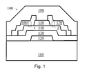
- Fig. 1 shows the structure of an inverted staggered thin film transistor 100.
- the TFT 100 includes a substrate 110.
- the substrate may be a glass substrate.
- the substrate may be plastic substrate, ceramic substrate or metal substrate, possibly provided with an insulating film such silicon oxide.
- the substrate may include at least one material chosen from silicon oxide, barium borosilicate glass, aluminoborosilicate glass, aluminosilicate glass, and combinations thereof.
- a gate 120 is formed on the substrate 110.
- the gate 120 may include at least one material chosen from copper, titanium, molybdenum, chromium, tantalum, tungsten, aluminum, silver, gold, ITO, an alloy material thereof, e.g., an aluminum-neodymium alloy or an aluminum-selenium alloy, and combinations thereof.
- the gate may be deposited on the substrate, e.g., by sputtering, such as magnetron sputtering.
- the TFT 100 includes a gate dielectric 130 formed on the gate 120 and the substrate 110.
- the gate dielectric may include at least one material chosen from silicon oxide, silicon nitride, silicon oxynitride, aluminum oxide, titanium oxide, and combinations thereof.
- TFT 100 includes an active channel region 140, e.g., an active channel island including a transparent oxide.
- the active channel region 140 is formed on the gate dielectric 130.
- the active channel region may include at least one material chosen from transparent oxide, zinc oxide, zinc tin oxide, zinc indium tin oxide, indium zinc oxide, indium gallium zinc oxide, hafnium indium zinc oxide, aluminum zinc tin oxide, copper oxide, and combinations thereof.
- An etch stop layer 150 may be formed on the active channel 140.
- the etch stop layer may include at least one material chosen from silicon oxide, silicon nitride, silicon oxynitride, aluminum oxide, titanium oxide, and combinations thereof.
- a source 160 and a drain 170 are formed on the active channel 140.
- the source and drain may include at least one material chosen from copper, titanium, molybdenum, chromium, tantalum, tungsten, aluminum, silver, gold, ITO, alloys thereof, and combinations thereof.
- the etch stop layer 150 can be between the source 160 and the drain 170.
- a passivation layer 180 may be formed on the whole structure, also separating the source 160 and the drain 170.
- the passivation layer may include at least one material chosen from silicon oxide, silicon nitride, silicon oxynitride, aluminum oxide, titanium oxide, and combinations thereof.
- a contact resistance may exist between the source 160 and the active channel region 140 and/or between the drain 170 and the active channel region 140.
- the metallization of the electrodes 160, 170 is copper-based, e.g., for connection to copper wires, and the active channel is made of a transparent oxide such as zinc oxide, a contact resistance exists.
- the contact resistance may decrease the performance of the TFT.
- a thin film transistor is provided.
- the thin film transistor may be an inverted staggered TFT.
- the thin film transistor includes an annealed layer stack.
- the annealed layer stack includes a conductive oxide layer, a copper alloy layer, a copper containing oxide layer, and a copper containing layer.
- the conductive oxide layer may be the active channel region.
- the copper alloy layer, copper containing oxide layer and copper containing layer may be sub-layers of the source or the drain electrode.
- the copper alloy layer may be deposited on the conductive oxide layer.
- the copper containing oxide layer may alternatively be absent. If it is present, it may be deposited on the copper alloy layer.
- the copper containing layer may be deposited on the copper containing oxide layer, or on the copper alloy layer if the copper containing oxide layer is not present.
- Fig. 2 shows a layer stack 200 of this type.
- the layer stack 200 includes conductive oxide layer 210, which may, e.g., be identical with the active channel 140.
- the layer stack 200 further includes copper alloy layer 220, copper containing oxide layer 230, and copper containing layer 240.
- Layers 220, 230, 240 may, e.g., be sub-layers of source electrode 160 or drain electrode 170.
- the layer stack 200 shown in Fig. 2 may, e.g., be part of the TFT structure shown in Fig. 1 , and may correspond to the regions 1 or 2 represented by dashed boxes in Fig. 1 .
- the TFT structure may include more than one layer stack according to embodiments described herein, e.g., at least two separate layer stacks as represented by the dashed boxes 1 and 2 in Fig. 1 , and corresponding to a source/active channel layer stack and a drain/active channel layer stack.
- the copper alloy layer 220 is formed on, and contacts, the conductive oxide layer 210.
- the copper containing oxide layer 230 is formed on, and contacts, the copper alloy layer 220.
- the copper containing layer 240 is formed on, and contacts, the copper containing oxide layer 230.
- the conductive oxide layer may be a transparent oxide layer, particularly a ZnO-containing layer, a ZTO-containing layer, a ZITO-containing layer, an IZO-containing layer, an IGZO-containing layer, a HIZO-containing layer, an AZTO-containing layer, a Cu 2 O-containing layer, and combinations thereof.
- the conductive oxide layer may be formed on a gate dielectric, e.g., as shown in Fig. 1 .
- the copper alloy layer may be formed on the conductive oxide layer, e.g., after formation of an etch stop layer.
- the copper alloy layer may be formed by depositing a first buffer film, e.g., by sputtering a Cu alloy, wherein the alloying material may be Mn, Mg, Cr, Mo, Ca and combinations thereof.
- Sputtering may be magnetron sputtering, e.g. static magnetron sputtering, reactive magnetron sputtering or static reactive magnetron sputtering.
- the copper target may, e.g., be Cu4N.
- At least the conductive oxide layer and the first buffer film may be annealed.
- the first buffer film is at least partly oxidized.
- the alloying element may be oxidized.
- the oxygen contained in the conductive oxide layer may oxidize the alloying element. This process will be called copper alloy self-forming barrier process.
- the copper alloy layer may include at least one material selected from the group consisting of: an alloy material that is at least partly oxidized, Cu, Mn, Mg, Cr, Mo, Ca, oxides of Cu, Mn, Mg, Cr, Mo, Ca, and combinations thereof.
- the copper alloy layer may be a sputtered, annealed copper alloy layer. Annealing may be vacuum annealing.
- the copper alloy layer may be an oxidized or partly oxidized copper alloy layer, e.g., a partly oxidized copper alloy layer in which the alloying material(s) is/are oxidized.
- the copper alloy layer may include at least 80% by weight copper, or at least 90 % by weight copper, or at least 95 % by weight copper, or even at least 99.5 % by weight copper.
- the copper alloy layer may, e.g., include at most 20% by weight of material other than copper, or at most 10 % by weight of material other than copper, e.g., alloying material, or at most 5 % by weight, or even at most 0.5 % by weight.
- the annealing may be carried out, e.g., after forming the whole layer stack according to embodiments described herein, or after forming at least some further layers.
- An "annealed layer stack” shall refer to a layer stack, at least one layer of which besides the copper alloy layer is annealed, more specifically at least one layer besides the first buffer layer.
- the copper containing oxide layer is formed on the first buffer film, respectively on the conductive oxide layer.
- the copper containing oxide layer may be a second buffer film. It may be deposited, for instance by sputtering such as reactive magnetron sputtering. For example, substantially pure copper such as Cu4N may be sputtered in a gas atmosphere including argon and oxygen.
- the copper containing oxide layer may include at least one material chosen from: CuO, Cu 2 O, and combinations thereof.
- the copper containing oxide layer may include at least 79 % by weight copper, or at least 90 % by weight copper, or even at least 99.9 % by weight copper.
- the copper containing oxide layer may, e.g., include at most 20 % by weight of material other than copper, e.g., oxygen, or at most 10 % by weight, or even at most 0.1 % by weight.
- oxygen from the copper containing oxide layer may oxidize the copper alloy layer. This process may occur additionally or alternatively to the oxidization by oxygen from the conductive oxide layer. At least one layer chosen from the conductive oxide layer and the copper containing oxide layer may have an oxygen depletion zone adjacent to the copper alloy layer. In particular, the oxygen depletion zone may be due to the Cu alloy self-forming barrier process at the interface with the conductive oxide layer and/or the copper containing oxide layer. The thickness of the Cu alloy layer may such that the Cu alloy layer is completely oxidized after the self-forming barrier process. The thickness may be very thin to achieve this.
- the copper containing layer may be formed on the copper containing oxide layer, e.g., by sputtering.
- sputtering may be carried out by sputtering directly on the copper containing oxide layer, e.g., in pure argon atmosphere.
- the same sputter target e.g., a rotary sputter target, may be used as in the case of sputtering the copper containing oxide layer.
- the sputter target may be used without sputter cleaning between formation of the copper containing oxide layer and the copper containing layer.
- Cu4N may be used as sputter target.
- the copper containing layer may include at least 90 % by weight copper, or at least 95 % by weight copper, or even at least 99.99 % by weight copper.
- the copper containing oxide layer may, e.g., include at most 10 % by weight of material other than copper, or at most 5 % by weight, or even at most 0.01 % by weight.
- the copper containing layer may substantially consist of copper. Therein, “substantially consisting of copper” means consisting of copper apart from impurities.
- the copper containing layer may be thicker than the copper containing oxide layer and/or the copper alloy layer. It may form the main portion of a source or drain electrode, or a terminal for circuitry such as copper wires.
- Fig. 3 shows an annealed layer stack 200 including the conductive oxide layer 210.
- the conductive oxide layer 210 includes an oxygen depletion zone 215 adjacent to the contact region with the copper alloy layer 220.
- the oxygen depletion is schematically illustrated by open circles in the zone 215, and the at least partial oxidization of copper alloy layer 220 is indicated by a pattern of vertical lines.
- the copper containing oxide layer 230 may also include an oxygen depletion zone adjacent to the copper alloy layer.
- the layer stack 200 shown in Fig. 3 is annealed after formation of its layers 210-240.
- the layers may have thicknesses in the following ranges according to some embodiments.
- the conductive oxide layer may have a thickness from 20 nm to 150 nm.
- the copper alloy layer may have a thickness from 2 nm to 30 nm.
- the copper containing oxide layer may have a thickness from 2 nm to 50 nm, e.g. from 2 nm to 30 nm.
- the copper containing layer may have a thickness from 50 nm to 500 nm, e.g., from 100 nm to 400 nm.
- the thickness of an oxygen depletion zone may be in the range from 0.1 nm to 3 nm.
- the contact resistance depends on the material characteristics of contacting layers.
- the conductivity of the conductive oxide layer e.g., a transparent oxide layer such as ZnO, depends on the concentration of oxygen vacancies in the material.
- the conductivity may be proportional to the concentration of vacancies.
- the oxygen content of the conductive oxide layer and/or the copper containing oxide layer may be adapted such that the desired oxidization of the copper alloy layer is achieved.
- the properties of the copper alloy layer, in particular of the alloying element or the alloying elements may be adapted such that the desired oxidization of the copper alloy is achieved.
- the oxygen donation or reception properties of the layers may be adapted such that the desired concentration of oxygen vacancies in oxygen depletion zones of the respective layers is achieved.
- Further control is provided by controlling the deposition parameters of the layers and the annealing parameters. For instance, the power at the sputtering cathodes, the pressure of the sputtering gas or the partial pressures of the sputtering gases, the composition of the sputtering gases such as the argon/oxygen mixture, and the deposition time may be varied. Additionally or alternatively, the annealing time and/or the annealing temperature may be controlled. In this way, the extent of the reduction of the contact resistance and the properties of the adhesion/barrier layer may be controlled and adapted to the process requirements for TFT production.
- the resistivity properties between any pair of layers of the layer stack may be matched such that the contact resistance is low. This will be referred to as matching of the contact resistance or RC-matching.
- the contact resistance may be matched by annealing.
- the contact resistance, or actually values (R C .W), between RC-matched layers may, e.g., be from 1 to 10000 ⁇ cm.
- the conductive oxide layer and the copper alloy layer may be RC-matched.
- an oxygen depletion zone of the conductive oxide layer provides RC-matching to the copper alloy layer.
- the oxidization of the copper alloy layer by oxygen from the oxygen depletion zone of the conductive oxide layer may further contribute to RC-matching.
- the copper alloy layer and the copper containing oxide layer are RC-matched.
- an oxygen depletion zone of the copper containing oxide layer may provide RC-matching to the copper alloy layer.
- the oxidization of the copper alloy layer by oxygen from the oxygen depletion zone of the copper containing oxide layer may further contribute to RC-matching.
- any of the oxygen depletion zones may be adapted to match the resistivity properties of the corresponding adjacent layers, i.e., it may be adapted for RC-matching.
- the annealed layer stack may be an annealed RC-matched layer stack.
- the layer stack is referred to as RC-matched if at least one layer pair chosen from the pair conductive oxide layer/copper alloy layer and from the pair copper alloy layer/copper containing oxide layer is RC-matched.
- a method of forming a staggered thin film transistor includes providing a conductive oxide layer of the thin film transistor, depositing a copper alloy layer on the conductive oxide layer, depositing a copper containing oxide layer on the copper alloy layer, and depositing a copper containing layer on the copper containing oxide layer.
- the method further includes annealing the copper alloy layer and at least one of the layers chosen from the conductive oxide layer, the copper containing oxide layer, and the copper containing layer. Annealing may include annealing the conductive oxide layer, the copper alloy layer, the copper containing oxide layer and the copper containing layer.
- Annealing may include oxidizing at least one alloy material of the copper alloy layer with oxygen from at least one layer chosen from: the conductive oxide layer and the copper containing oxide layer.
- the copper alloy layer in particular the alloying element or the alloying elements of the copper alloy layer, may be exclusively oxidized with oxygen from the conductive oxide layer and/or the copper containing oxide layer.
- Annealing may include forming at least one oxygen depletion zone in the conductive oxide layer and/or the copper containing oxide layer. Therein, the oxygen depletion zone may be adapted for RC-matching the conductive oxide layer and the copper alloy layer and/or for RC-matching the copper alloy layer and the copper containing oxide layer.
- Annealing may include forming an RC-matched layer stack, wherein the RC-matched layer stack may be any layer stack according to embodiments described herein.
- Depositing of the copper alloy layer may include sputtering of a copper alloy.
- Sputtering may be magnetron sputtering, such as static and/or reactive magnetron sputtering of the copper alloy.
- the copper alloy may, e.g., be chosen from: Mn, Mg, Cr or mixtures thereof.
- Depositing of the copper containing oxide layer may include sputtering of copper in an oxygen-containing gas environment.
- the gas environment may include Ar and O 2 .
- Sputtering may include magnetron sputtering of copper, e.g., reactive magnetron sputtering, such as reactive magnetron with rotary targets.
- Depositing of the copper containing layer may include sputtering of copper in an inert gas environment.
- the inert gas environment includes Ar.
- Sputtering my include magnetron sputtering of copper, e.g., reactive magnetron sputtering, such as reactive magnetron with rotary targets.
- sputtering of the copper containing layer may include sputtering with the same targets as in the sputtering of the copper containing oxide layer.
- the targets may be untreated (in particular not cleaned) between sputtering the copper containing oxide layer and sputtering the copper containing layer.
- the copper alloy layer, the copper containing oxide layer, and the copper containing layer may form an electrode of the thin film transistor in contact with the conductive oxide layer forming the active channel region of the thin film transistor.
- embodiments of the present invention are not limited thereto.
- the self-formation of a barrier layer and/or of at least one oxygen depletion zone may be applied to other layers of the TFT structure as well.
- a method of forming a gate metallization includes depositing a gate electrode metallization on a substrate of a thin film transistor.
- the thin film transistor may be a thin film transistor according to embodiments described herein, in particular a staggered/ inverted staggered TFT with a layer stack as described herein.
- the method of forming a gate metallization may further include annealing the gate electrode metallization to at least partly oxidize the gate electrode metallization by oxygen from the substrate.
- the annealing of the gate electrode metallization may be identical with the annealing of the layer stack, or it may be a separate annealing.
- the annealed layer stack according to the embodiments described above can also be at the interface between the substrate and the gate electrode of the thin film transistor.
- the conductive oxide layer is replaced by the substrate.
- the substrate may be made of the substrate materials described in the foregoing, and contains oxygen.
- the substrate may contain oxygen in the form of an oxide such as silicon oxide.
- the copper alloy layer may then be oxidized by the oxygen from the substrate and/or from the copper containing oxide layer. RC-matching occurs only between the copper alloy layer, the copper containing oxide layer and the copper containing layer. These three layers form, or form a part of, the gate electrode.
- the gate electrode may be a multi-layer electrode.
- Figs. 2 and 3 also illustrate these embodiments, wherein the layer with reference sign 210 is now the substrate or an oxygen-containing coating of the substrate, e.g., the substrate 110 of Fig. 1 .
- the copper alloy layer 220, the copper containing oxide layer 230, and the copper containing layer 240 may, e.g., be included in the gate electrode 120 of Fig. 1 .
- the annealed layer stack includes an oxygen containing layer, in particular an oxide containing layer.
- the oxide containing layer may be the conductive oxide layer as described above.
- the oxide containing layer may be the substrate or a part thereof, such as a coating of the substrate.
- the annealed layer stack includes the copper alloy layer, the copper containing oxide layer and the copper containing layer, which may have the properties described above. If the oxide containing layer is the conductive oxide layer, these three layers may be part of the source and/or drain electrode of the thin film transistor. If the oxide containing layer is the substrate or a part thereof, these three layers may form, or be part of, the gate electrode.
- the thin film transistor may include at least two annealed layer stacks according to the embodiments described herein.
- the thin film transistor may include a first annealed layer stack at the interface of the substrate and the gate electrode, and a second annealed layer stack at the interface of the active channel and the source/drain electrode(s).
- the method of forming the first and second annealed layer stacks may be substantially the same (the oxide containing layer being the substrate in the first annealed layer stack and being the conductive oxide layer of the active channel in the second annealed layer stack).
- annealed layer stacks and the methods of forming the same can be adopted both for drain/source electrodes and gate electrodes constitutes an advantage.
- the complexity of the production process can be reduced.
- the same apparatuses can be used for the formation of these parts of the thin film transistors. Production costs as well as costs of the equipment of the production site may be lowered, and throughput be increased.
- Fig. 4 schematically illustrates a method of forming a thin film transistor.
- the method includes providing 410 a substrate and forming 420 a gate electrode on the substrate.
- Forming the gate electrode may include depositing 422 a copper alloy layer on the substrate, depositing 424 a copper containing oxide layer on the copper alloy layer, and depositing 426 a copper containing layer on the copper containing oxide layer.
- the method may include annealing 428 the substrate, the copper alloy layer, the copper containing oxide layer and the copper containing layer.
- the method may further include forming 430 a gate dielectric on the substrate and the gate electrode, and forming 440 an active channel region on the gate dielectric.
- the gate dielectric is formed such that it provides an electrical insulation between the gate electrode and the active channel region.
- the active channel region includes, or consists of, a conductive oxide layer.
- the method may include forming 450 an etch stop layer on the active channel region.
- the method may further include forming 460 a source electrode and forming a drain electrode on the conductive oxide layer of the active channel region.
- the formation of source and drain electrode may include forming an electrode layer and separating the electrode layer into a source electrode and a drain electrode by etching, such as etching to the etch stop layer.
- Forming the source electrode and the drain electrode, respectively forming the electrode layer may include depositing 462 a second copper alloy layer on the conductive oxide layer, depositing 464 a second copper containing oxide layer on the second copper alloy layer, and depositing 466 a second copper containing layer on the second copper containing oxide layer.
- the method may include annealing 468 the conductive oxide layer, the second copper alloy layer, the second copper containing oxide layer and the second copper containing layer.
- the method may include forming 480 a passivation layer on the source electrode, the drain electrode, and/or on the etch stop layer, separating the source and the drain electrode.
- the method includes either formation steps 420-426 of the gate electrode or formation steps 460-466 of the drain/source electrodes, or includes both the formation steps 420-426 and 460-466.
- the method includes at least one annealing step, e.g., step 428 or step 468 or both.
Landscapes
- Engineering & Computer Science (AREA)
- Microelectronics & Electronic Packaging (AREA)
- Power Engineering (AREA)
- Physics & Mathematics (AREA)
- Condensed Matter Physics & Semiconductors (AREA)
- General Physics & Mathematics (AREA)
- Computer Hardware Design (AREA)
- Ceramic Engineering (AREA)
- Manufacturing & Machinery (AREA)
- Thin Film Transistor (AREA)
- Electrodes Of Semiconductors (AREA)
- Formation Of Insulating Films (AREA)
Priority Applications (7)
| Application Number | Priority Date | Filing Date | Title |
|---|---|---|---|
| EP10175294A EP2426720A1 (de) | 2010-09-03 | 2010-09-03 | Versetzter Dünnfilmtransistor und Herstellungsverfahren dafür |
| US12/879,593 US20120056173A1 (en) | 2010-09-03 | 2010-09-10 | Staggered thin film transistor and method of forming the same |
| KR1020137008425A KR20130102576A (ko) | 2010-09-03 | 2011-08-09 | 스태거드 박막 트랜지스터 및 그 형성 방법 |
| CN201180044614.4A CN103140929B (zh) | 2010-09-03 | 2011-08-09 | 错列薄膜晶体管及形成错列薄膜晶体管的方法 |
| JP2013526392A JP2013541192A (ja) | 2010-09-03 | 2011-08-09 | スタガー薄膜トランジスタおよびその形成方法 |
| PCT/EP2011/063712 WO2012028432A1 (en) | 2010-09-03 | 2011-08-09 | Staggered thin film transistor and method of forming the same |
| TW100129784A TW201232784A (en) | 2010-09-03 | 2011-08-19 | Staggered thin film transistor and method of forming the same |
Applications Claiming Priority (1)
| Application Number | Priority Date | Filing Date | Title |
|---|---|---|---|
| EP10175294A EP2426720A1 (de) | 2010-09-03 | 2010-09-03 | Versetzter Dünnfilmtransistor und Herstellungsverfahren dafür |
Publications (1)
| Publication Number | Publication Date |
|---|---|
| EP2426720A1 true EP2426720A1 (de) | 2012-03-07 |
Family
ID=43104661
Family Applications (1)
| Application Number | Title | Priority Date | Filing Date |
|---|---|---|---|
| EP10175294A Withdrawn EP2426720A1 (de) | 2010-09-03 | 2010-09-03 | Versetzter Dünnfilmtransistor und Herstellungsverfahren dafür |
Country Status (7)
| Country | Link |
|---|---|
| US (1) | US20120056173A1 (de) |
| EP (1) | EP2426720A1 (de) |
| JP (1) | JP2013541192A (de) |
| KR (1) | KR20130102576A (de) |
| CN (1) | CN103140929B (de) |
| TW (1) | TW201232784A (de) |
| WO (1) | WO2012028432A1 (de) |
Cited By (1)
| Publication number | Priority date | Publication date | Assignee | Title |
|---|---|---|---|---|
| EP2828892A4 (de) * | 2012-03-19 | 2015-03-04 | Ricoh Co Ltd | Elektrisch leitfähige dünnschicht, beschichtungsflüssigkeit zur bildung der elektrisch leitfähigen dünnschicht, feldeffekttransistor und verfahren zur herstellung des feldeffekttransistors |
Families Citing this family (35)
| Publication number | Priority date | Publication date | Assignee | Title |
|---|---|---|---|---|
| US8962386B2 (en) * | 2011-11-25 | 2015-02-24 | Semiconductor Energy Laboratory Co., Ltd. | Semiconductor device and method for manufacturing the same |
| WO2013183254A1 (ja) * | 2012-06-08 | 2013-12-12 | パナソニック株式会社 | 薄膜トランジスタ及び薄膜トランジスタの製造方法 |
| JP5972065B2 (ja) * | 2012-06-20 | 2016-08-17 | 富士フイルム株式会社 | 薄膜トランジスタの製造方法 |
| US9379247B2 (en) * | 2012-06-28 | 2016-06-28 | Cbrite Inc. | High mobility stabile metal oxide TFT |
| US8823003B2 (en) | 2012-08-10 | 2014-09-02 | Apple Inc. | Gate insulator loss free etch-stop oxide thin film transistor |
| WO2014067463A1 (zh) * | 2012-11-02 | 2014-05-08 | 京东方科技集团股份有限公司 | 薄膜晶体管及其制作方法、阵列基板、显示装置和阻挡层 |
| US9601557B2 (en) | 2012-11-16 | 2017-03-21 | Apple Inc. | Flexible display |
| TWI594333B (zh) * | 2013-12-31 | 2017-08-01 | 國立交通大學 | 降低氧化物薄膜電晶體之接觸電阻的方法 |
| KR102163730B1 (ko) * | 2014-03-25 | 2020-10-08 | 삼성전자주식회사 | 트랜지스터와 그 제조방법 및 트랜지스터를 포함하는 전자소자 |
| US9600112B2 (en) | 2014-10-10 | 2017-03-21 | Apple Inc. | Signal trace patterns for flexible substrates |
| KR102260886B1 (ko) * | 2014-12-10 | 2021-06-07 | 삼성디스플레이 주식회사 | 박막 트랜지스터 |
| KR20180075733A (ko) | 2016-12-26 | 2018-07-05 | 엘지디스플레이 주식회사 | 플렉서블 표시장치 |
| US10224224B2 (en) | 2017-03-10 | 2019-03-05 | Micromaterials, LLC | High pressure wafer processing systems and related methods |
| US10847360B2 (en) | 2017-05-25 | 2020-11-24 | Applied Materials, Inc. | High pressure treatment of silicon nitride film |
| US10622214B2 (en) | 2017-05-25 | 2020-04-14 | Applied Materials, Inc. | Tungsten defluorination by high pressure treatment |
| WO2018222771A1 (en) | 2017-06-02 | 2018-12-06 | Applied Materials, Inc. | Dry stripping of boron carbide hardmask |
| WO2019036157A1 (en) | 2017-08-18 | 2019-02-21 | Applied Materials, Inc. | HIGH PRESSURE AND HIGH TEMPERATURE RECOVERY CHAMBER |
| US10276411B2 (en) | 2017-08-18 | 2019-04-30 | Applied Materials, Inc. | High pressure and high temperature anneal chamber |
| CN111095524B (zh) | 2017-09-12 | 2023-10-03 | 应用材料公司 | 用于使用保护阻挡物层制造半导体结构的设备和方法 |
| US10643867B2 (en) | 2017-11-03 | 2020-05-05 | Applied Materials, Inc. | Annealing system and method |
| EP3707746B1 (de) | 2017-11-11 | 2023-12-27 | Micromaterials LLC | Gaszufuhrsystem für hochdruckprozesskammer |
| WO2019099125A1 (en) | 2017-11-16 | 2019-05-23 | Applied Materials, Inc. | High pressure steam anneal processing apparatus |
| JP2021503714A (ja) | 2017-11-17 | 2021-02-12 | アプライド マテリアルズ インコーポレイテッドApplied Materials,Incorporated | 高圧処理システムのためのコンデンサシステム |
| WO2019147400A1 (en) | 2018-01-24 | 2019-08-01 | Applied Materials, Inc. | Seam healing using high pressure anneal |
| WO2019173006A1 (en) * | 2018-03-09 | 2019-09-12 | Applied Materials, Inc. | High pressure annealing process for metal containing materials |
| US10714331B2 (en) | 2018-04-04 | 2020-07-14 | Applied Materials, Inc. | Method to fabricate thermally stable low K-FinFET spacer |
| US10950429B2 (en) | 2018-05-08 | 2021-03-16 | Applied Materials, Inc. | Methods of forming amorphous carbon hard mask layers and hard mask layers formed therefrom |
| US10566188B2 (en) | 2018-05-17 | 2020-02-18 | Applied Materials, Inc. | Method to improve film stability |
| US10704141B2 (en) | 2018-06-01 | 2020-07-07 | Applied Materials, Inc. | In-situ CVD and ALD coating of chamber to control metal contamination |
| US10748783B2 (en) | 2018-07-25 | 2020-08-18 | Applied Materials, Inc. | Gas delivery module |
| US10675581B2 (en) | 2018-08-06 | 2020-06-09 | Applied Materials, Inc. | Gas abatement apparatus |
| WO2020092002A1 (en) | 2018-10-30 | 2020-05-07 | Applied Materials, Inc. | Methods for etching a structure for semiconductor applications |
| SG11202103763QA (en) | 2018-11-16 | 2021-05-28 | Applied Materials Inc | Film deposition using enhanced diffusion process |
| WO2020117462A1 (en) | 2018-12-07 | 2020-06-11 | Applied Materials, Inc. | Semiconductor processing system |
| US11901222B2 (en) | 2020-02-17 | 2024-02-13 | Applied Materials, Inc. | Multi-step process for flowable gap-fill film |
Citations (5)
| Publication number | Priority date | Publication date | Assignee | Title |
|---|---|---|---|---|
| JPH06333925A (ja) * | 1993-05-20 | 1994-12-02 | Nippon Steel Corp | 半導体集積回路及びその製造方法 |
| US20080038882A1 (en) * | 2006-08-09 | 2008-02-14 | Kazushige Takechi | Thin-film device and method of fabricating the same |
| US20090090942A1 (en) * | 2007-09-04 | 2009-04-09 | Samsung Electronics Co. Ltd. | Wiring structure, array substrate, display device having the same and method of manufacturing the same |
| US20090153056A1 (en) * | 2007-12-17 | 2009-06-18 | Au Optronics Corporation | Pixel structure, display panel, eletro-optical apparatus, and method thererof |
| US20100051934A1 (en) * | 2008-08-26 | 2010-03-04 | Jong-Hyun Choung | Thin film transistor array panel and method of manufacturing the same |
Family Cites Families (22)
| Publication number | Priority date | Publication date | Assignee | Title |
|---|---|---|---|---|
| JP4954366B2 (ja) * | 2000-11-28 | 2012-06-13 | 株式会社半導体エネルギー研究所 | 半導体装置の作製方法 |
| JP4496518B2 (ja) * | 2002-08-19 | 2010-07-07 | 日立金属株式会社 | 薄膜配線 |
| JP3940385B2 (ja) * | 2002-12-19 | 2007-07-04 | 株式会社神戸製鋼所 | 表示デバイスおよびその製法 |
| KR100905662B1 (ko) * | 2003-06-26 | 2009-06-30 | 엘지디스플레이 주식회사 | 액정표시장치 제조 방법 및 배선 구조 |
| KR20070049278A (ko) * | 2005-11-08 | 2007-05-11 | 삼성전자주식회사 | 배선, 이를 포함하는 박막 트랜지스터 기판과 그 제조 방법 |
| KR20080037296A (ko) * | 2006-10-25 | 2008-04-30 | 삼성전자주식회사 | 박막 트랜지스터 기판 및 그 제조방법 |
| US7919795B2 (en) * | 2006-12-21 | 2011-04-05 | Samsung Electronics Co., Ltd. | Wire structure, method for fabricating wire, thin film transistor substrate, and method for fabricating the thin film transistor substrate |
| WO2008081806A1 (ja) * | 2006-12-28 | 2008-07-10 | Ulvac, Inc. | 配線膜の形成方法、トランジスタ、及び電子装置 |
| KR100858088B1 (ko) * | 2007-02-28 | 2008-09-10 | 삼성전자주식회사 | 박막 트랜지스터 및 그 제조 방법 |
| JP4871777B2 (ja) * | 2007-04-16 | 2012-02-08 | 株式会社アルバック | エッチング液及びトランジスタ製造方法 |
| JP5121299B2 (ja) * | 2007-05-09 | 2013-01-16 | アルティアム サービシズ リミテッド エルエルシー | 液晶表示装置 |
| KR101296654B1 (ko) * | 2007-12-26 | 2013-08-14 | 엘지디스플레이 주식회사 | 구리 배선, 이를 이용한 평판 표시 장치, 및 그 구리배선의 형성 방법 |
| WO2010013636A1 (ja) * | 2008-07-29 | 2010-02-04 | 株式会社アルバック | 配線膜、薄膜トランジスタ、ターゲット、配線膜の形成方法 |
| JP5571887B2 (ja) * | 2008-08-19 | 2014-08-13 | アルティアム サービシズ リミテッド エルエルシー | 液晶表示装置及びその製造方法 |
| JP5269533B2 (ja) * | 2008-09-26 | 2013-08-21 | 三菱マテリアル株式会社 | 薄膜トランジスター |
| JP5360959B2 (ja) * | 2008-10-24 | 2013-12-04 | 三菱マテリアル株式会社 | バリア膜とドレイン電極膜およびソース電極膜が高い密着強度を有する薄膜トランジスター |
| US8237163B2 (en) * | 2008-12-18 | 2012-08-07 | Lg Display Co., Ltd. | Array substrate for display device and method for fabricating the same |
| CN103456794B (zh) * | 2008-12-19 | 2016-08-10 | 株式会社半导体能源研究所 | 晶体管的制造方法 |
| JP4752927B2 (ja) * | 2009-02-09 | 2011-08-17 | ソニー株式会社 | 薄膜トランジスタおよび表示装置 |
| WO2010098101A1 (ja) * | 2009-02-27 | 2010-09-02 | 株式会社アルバック | トランジスタ、トランジスタの製造方法及びその製造装置 |
| CN102422426B (zh) * | 2009-05-01 | 2016-06-01 | 株式会社半导体能源研究所 | 半导体装置的制造方法 |
| KR101687311B1 (ko) * | 2009-10-07 | 2016-12-16 | 삼성디스플레이 주식회사 | 표시 장치 및 이의 제조 방법 |
-
2010
- 2010-09-03 EP EP10175294A patent/EP2426720A1/de not_active Withdrawn
- 2010-09-10 US US12/879,593 patent/US20120056173A1/en not_active Abandoned
-
2011
- 2011-08-09 WO PCT/EP2011/063712 patent/WO2012028432A1/en active Application Filing
- 2011-08-09 KR KR1020137008425A patent/KR20130102576A/ko active Search and Examination
- 2011-08-09 JP JP2013526392A patent/JP2013541192A/ja active Pending
- 2011-08-09 CN CN201180044614.4A patent/CN103140929B/zh not_active Expired - Fee Related
- 2011-08-19 TW TW100129784A patent/TW201232784A/zh unknown
Patent Citations (5)
| Publication number | Priority date | Publication date | Assignee | Title |
|---|---|---|---|---|
| JPH06333925A (ja) * | 1993-05-20 | 1994-12-02 | Nippon Steel Corp | 半導体集積回路及びその製造方法 |
| US20080038882A1 (en) * | 2006-08-09 | 2008-02-14 | Kazushige Takechi | Thin-film device and method of fabricating the same |
| US20090090942A1 (en) * | 2007-09-04 | 2009-04-09 | Samsung Electronics Co. Ltd. | Wiring structure, array substrate, display device having the same and method of manufacturing the same |
| US20090153056A1 (en) * | 2007-12-17 | 2009-06-18 | Au Optronics Corporation | Pixel structure, display panel, eletro-optical apparatus, and method thererof |
| US20100051934A1 (en) * | 2008-08-26 | 2010-03-04 | Jong-Hyun Choung | Thin film transistor array panel and method of manufacturing the same |
Cited By (2)
| Publication number | Priority date | Publication date | Assignee | Title |
|---|---|---|---|---|
| EP2828892A4 (de) * | 2012-03-19 | 2015-03-04 | Ricoh Co Ltd | Elektrisch leitfähige dünnschicht, beschichtungsflüssigkeit zur bildung der elektrisch leitfähigen dünnschicht, feldeffekttransistor und verfahren zur herstellung des feldeffekttransistors |
| US9978877B2 (en) | 2012-03-19 | 2018-05-22 | Ricoh Company, Ltd. | Electroconductive thin film, coating liquid for forming electroconductive thin film, field-effect transistor, and method for producing field-effect transistor |
Also Published As
| Publication number | Publication date |
|---|---|
| KR20130102576A (ko) | 2013-09-17 |
| CN103140929A (zh) | 2013-06-05 |
| US20120056173A1 (en) | 2012-03-08 |
| WO2012028432A1 (en) | 2012-03-08 |
| TW201232784A (en) | 2012-08-01 |
| CN103140929B (zh) | 2015-12-02 |
| JP2013541192A (ja) | 2013-11-07 |
Similar Documents
| Publication | Publication Date | Title |
|---|---|---|
| EP2426720A1 (de) | Versetzter Dünnfilmtransistor und Herstellungsverfahren dafür | |
| US10763371B2 (en) | Thin-film transistor, method of manufacturing the same, and display device | |
| KR102518392B1 (ko) | 박막트랜지스터 어레이 기판 | |
| TWI437697B (zh) | Wiring structure and a display device having a wiring structure | |
| TWI559553B (zh) | 氧化物半導體薄膜電晶體、製造其之方法及包含其之有機電致發光裝置 | |
| JP5250929B2 (ja) | トランジスタおよびその製造方法 | |
| KR101700882B1 (ko) | 산화물 반도체 박막 트랜지스터 | |
| KR101175085B1 (ko) | 반도체 장치, 반도체 장치를 갖는 액정 표시 장치, 반도체 장치의 제조 방법 | |
| TWI455322B (zh) | 薄膜電晶體及其製造方法 | |
| US20140091306A1 (en) | Wiring structure and display device | |
| JP2009533884A (ja) | 半導体素子及びその製造方法 | |
| CN107278331B (zh) | 薄膜晶体管及其制造方法 | |
| KR20140074742A (ko) | 트랜지스터와 그 제조방법 및 트랜지스터를 포함하는 전자소자 | |
| JP6654770B2 (ja) | 薄膜トランジスタ基板及び表示装置 | |
| KR20120021454A (ko) | 트랜지스터와 그 제조방법 및 트랜지스터를 포함하는 전자소자 | |
| US20150349139A1 (en) | Oxide Thin Film Transistor and Manufacturing Method Thereof, Array Substrate and Display Device | |
| KR20080069810A (ko) | 박막 트랜지스터 기판 및 이의 제조 방법 | |
| KR20140106042A (ko) | 박막 트랜지스터 기판 및 그 제조방법 | |
| CN101090123A (zh) | 具铜导线结构的薄膜晶体管及其制造方法 | |
| US20200220020A1 (en) | Thin-film transistor and method for preparing the same, display substrate and display device | |
| CN110034191A (zh) | 薄膜晶体管、其制造方法及包括该薄膜晶体管的显示装置 | |
| KR20160060848A (ko) | 박막 트랜지스터 및 그 제조 방법 | |
| KR102278505B1 (ko) | 박막 트랜지스터, 박막 트랜지스터를 포함하는 박막 트랜지스터 표시판 및 박막 트랜지스터의 제조 방법 | |
| KR102180511B1 (ko) | 박막 트랜지스터 표시판 및 이의 제조 방법 | |
| KR20110044633A (ko) | 단일 구리 타겟을 이용한 박막트랜지스터 제조 방법 및 그 방법에 의한 박막 트랜지스터 |
Legal Events
| Date | Code | Title | Description |
|---|---|---|---|
| AK | Designated contracting states |
Kind code of ref document: A1 Designated state(s): AL AT BE BG CH CY CZ DE DK EE ES FI FR GB GR HR HU IE IS IT LI LT LU LV MC MK MT NL NO PL PT RO SE SI SK SM TR |
|
| AX | Request for extension of the european patent |
Extension state: BA ME RS |
|
| PUAI | Public reference made under article 153(3) epc to a published international application that has entered the european phase |
Free format text: ORIGINAL CODE: 0009012 |
|
| 17P | Request for examination filed |
Effective date: 20120907 |
|
| 17Q | First examination report despatched |
Effective date: 20140305 |
|
| GRAP | Despatch of communication of intention to grant a patent |
Free format text: ORIGINAL CODE: EPIDOSNIGR1 |
|
| INTG | Intention to grant announced |
Effective date: 20160321 |
|
| RIC1 | Information provided on ipc code assigned before grant |
Ipc: H01L 29/45 20060101ALI20160311BHEP Ipc: H01L 23/532 20060101ALI20160311BHEP Ipc: H01L 29/66 20060101AFI20160311BHEP Ipc: H01L 29/49 20060101ALI20160311BHEP Ipc: H01L 29/786 20060101ALI20160311BHEP |
|
| STAA | Information on the status of an ep patent application or granted ep patent |
Free format text: STATUS: THE APPLICATION IS DEEMED TO BE WITHDRAWN |
|
| 18D | Application deemed to be withdrawn |
Effective date: 20160802 |