EP2421034B1 - Substrate carrying mechanism and substrate carrying method - Google Patents
Substrate carrying mechanism and substrate carrying method Download PDFInfo
- Publication number
- EP2421034B1 EP2421034B1 EP11178081.3A EP11178081A EP2421034B1 EP 2421034 B1 EP2421034 B1 EP 2421034B1 EP 11178081 A EP11178081 A EP 11178081A EP 2421034 B1 EP2421034 B1 EP 2421034B1
- Authority
- EP
- European Patent Office
- Prior art keywords
- substrate
- detecting units
- wafer
- holding member
- notch
- Prior art date
- Legal status (The legal status is an assumption and is not a legal conclusion. Google has not performed a legal analysis and makes no representation as to the accuracy of the status listed.)
- Active
Links
- 239000000758 substrate Substances 0.000 title claims description 233
- 238000000034 method Methods 0.000 title claims description 60
- 230000007246 mechanism Effects 0.000 title claims description 57
- 238000012545 processing Methods 0.000 claims description 130
- 238000012546 transfer Methods 0.000 claims description 97
- 238000005259 measurement Methods 0.000 claims description 15
- 235000012431 wafers Nutrition 0.000 description 287
- 238000006073 displacement reaction Methods 0.000 description 92
- 238000001444 catalytic combustion detection Methods 0.000 description 82
- 230000002159 abnormal effect Effects 0.000 description 24
- 238000001514 detection method Methods 0.000 description 23
- 230000004048 modification Effects 0.000 description 23
- 238000012986 modification Methods 0.000 description 23
- 238000010438 heat treatment Methods 0.000 description 22
- 238000000576 coating method Methods 0.000 description 20
- 230000008569 process Effects 0.000 description 20
- 239000011248 coating agent Substances 0.000 description 18
- 238000003672 processing method Methods 0.000 description 14
- 230000002950 deficient Effects 0.000 description 9
- 230000014509 gene expression Effects 0.000 description 9
- 235000013290 Sagittaria latifolia Nutrition 0.000 description 8
- 235000015246 common arrowhead Nutrition 0.000 description 8
- 239000004065 semiconductor Substances 0.000 description 8
- 230000007257 malfunction Effects 0.000 description 6
- 230000008859 change Effects 0.000 description 4
- 101100221835 Arabidopsis thaliana CPL2 gene Proteins 0.000 description 3
- 101150075071 TRS1 gene Proteins 0.000 description 3
- 230000005540 biological transmission Effects 0.000 description 3
- 238000001816 cooling Methods 0.000 description 3
- 238000010586 diagram Methods 0.000 description 3
- 239000000126 substance Substances 0.000 description 3
- 101100221836 Arabidopsis thaliana CPL3 gene Proteins 0.000 description 2
- 101100065702 Arabidopsis thaliana ETC3 gene Proteins 0.000 description 2
- 238000010276 construction Methods 0.000 description 2
- 239000007888 film coating Substances 0.000 description 2
- 238000009501 film coating Methods 0.000 description 2
- 239000002245 particle Substances 0.000 description 2
- 230000002093 peripheral effect Effects 0.000 description 2
- 230000009467 reduction Effects 0.000 description 2
- 101100221837 Arabidopsis thaliana CPL4 gene Proteins 0.000 description 1
- 101100536545 Arabidopsis thaliana TCL2 gene Proteins 0.000 description 1
- -1 CPL11 Proteins 0.000 description 1
- 101000931525 Homo sapiens Forkhead box protein G1 Proteins 0.000 description 1
- 101001031356 Sphaenorhynchus lacteus Buforin-2 Proteins 0.000 description 1
- 239000000969 carrier Substances 0.000 description 1
- 230000003292 diminished effect Effects 0.000 description 1
- 239000000835 fiber Substances 0.000 description 1
- 239000012634 fragment Substances 0.000 description 1
- 230000003760 hair shine Effects 0.000 description 1
- 239000004973 liquid crystal related substance Substances 0.000 description 1
Images


Classifications
-
- H—ELECTRICITY
- H01—ELECTRIC ELEMENTS
- H01L—SEMICONDUCTOR DEVICES NOT COVERED BY CLASS H10
- H01L21/00—Processes or apparatus adapted for the manufacture or treatment of semiconductor or solid state devices or of parts thereof
- H01L21/67—Apparatus specially adapted for handling semiconductor or electric solid state devices during manufacture or treatment thereof; Apparatus specially adapted for handling wafers during manufacture or treatment of semiconductor or electric solid state devices or components ; Apparatus not specifically provided for elsewhere
- H01L21/68—Apparatus specially adapted for handling semiconductor or electric solid state devices during manufacture or treatment thereof; Apparatus specially adapted for handling wafers during manufacture or treatment of semiconductor or electric solid state devices or components ; Apparatus not specifically provided for elsewhere for positioning, orientation or alignment
- H01L21/681—Apparatus specially adapted for handling semiconductor or electric solid state devices during manufacture or treatment thereof; Apparatus specially adapted for handling wafers during manufacture or treatment of semiconductor or electric solid state devices or components ; Apparatus not specifically provided for elsewhere for positioning, orientation or alignment using optical controlling means
-
- H—ELECTRICITY
- H01—ELECTRIC ELEMENTS
- H01L—SEMICONDUCTOR DEVICES NOT COVERED BY CLASS H10
- H01L21/00—Processes or apparatus adapted for the manufacture or treatment of semiconductor or solid state devices or of parts thereof
- H01L21/67—Apparatus specially adapted for handling semiconductor or electric solid state devices during manufacture or treatment thereof; Apparatus specially adapted for handling wafers during manufacture or treatment of semiconductor or electric solid state devices or components ; Apparatus not specifically provided for elsewhere
- H01L21/677—Apparatus specially adapted for handling semiconductor or electric solid state devices during manufacture or treatment thereof; Apparatus specially adapted for handling wafers during manufacture or treatment of semiconductor or electric solid state devices or components ; Apparatus not specifically provided for elsewhere for conveying, e.g. between different workstations
- H01L21/67739—Apparatus specially adapted for handling semiconductor or electric solid state devices during manufacture or treatment thereof; Apparatus specially adapted for handling wafers during manufacture or treatment of semiconductor or electric solid state devices or components ; Apparatus not specifically provided for elsewhere for conveying, e.g. between different workstations into and out of processing chamber
- H01L21/67745—Apparatus specially adapted for handling semiconductor or electric solid state devices during manufacture or treatment thereof; Apparatus specially adapted for handling wafers during manufacture or treatment of semiconductor or electric solid state devices or components ; Apparatus not specifically provided for elsewhere for conveying, e.g. between different workstations into and out of processing chamber characterized by movements or sequence of movements of transfer devices
-
- H—ELECTRICITY
- H01—ELECTRIC ELEMENTS
- H01L—SEMICONDUCTOR DEVICES NOT COVERED BY CLASS H10
- H01L21/00—Processes or apparatus adapted for the manufacture or treatment of semiconductor or solid state devices or of parts thereof
- H01L21/67—Apparatus specially adapted for handling semiconductor or electric solid state devices during manufacture or treatment thereof; Apparatus specially adapted for handling wafers during manufacture or treatment of semiconductor or electric solid state devices or components ; Apparatus not specifically provided for elsewhere
- H01L21/677—Apparatus specially adapted for handling semiconductor or electric solid state devices during manufacture or treatment thereof; Apparatus specially adapted for handling wafers during manufacture or treatment of semiconductor or electric solid state devices or components ; Apparatus not specifically provided for elsewhere for conveying, e.g. between different workstations
- H01L21/67703—Apparatus specially adapted for handling semiconductor or electric solid state devices during manufacture or treatment thereof; Apparatus specially adapted for handling wafers during manufacture or treatment of semiconductor or electric solid state devices or components ; Apparatus not specifically provided for elsewhere for conveying, e.g. between different workstations between different workstations
-
- H—ELECTRICITY
- H01—ELECTRIC ELEMENTS
- H01L—SEMICONDUCTOR DEVICES NOT COVERED BY CLASS H10
- H01L21/00—Processes or apparatus adapted for the manufacture or treatment of semiconductor or solid state devices or of parts thereof
- H01L21/02—Manufacture or treatment of semiconductor devices or of parts thereof
- H01L21/027—Making masks on semiconductor bodies for further photolithographic processing not provided for in group H01L21/18 or H01L21/34
- H01L21/0271—Making masks on semiconductor bodies for further photolithographic processing not provided for in group H01L21/18 or H01L21/34 comprising organic layers
- H01L21/0273—Making masks on semiconductor bodies for further photolithographic processing not provided for in group H01L21/18 or H01L21/34 comprising organic layers characterised by the treatment of photoresist layers
- H01L21/0274—Photolithographic processes
-
- H—ELECTRICITY
- H01—ELECTRIC ELEMENTS
- H01L—SEMICONDUCTOR DEVICES NOT COVERED BY CLASS H10
- H01L21/00—Processes or apparatus adapted for the manufacture or treatment of semiconductor or solid state devices or of parts thereof
- H01L21/67—Apparatus specially adapted for handling semiconductor or electric solid state devices during manufacture or treatment thereof; Apparatus specially adapted for handling wafers during manufacture or treatment of semiconductor or electric solid state devices or components ; Apparatus not specifically provided for elsewhere
- H01L21/677—Apparatus specially adapted for handling semiconductor or electric solid state devices during manufacture or treatment thereof; Apparatus specially adapted for handling wafers during manufacture or treatment of semiconductor or electric solid state devices or components ; Apparatus not specifically provided for elsewhere for conveying, e.g. between different workstations
- H01L21/67739—Apparatus specially adapted for handling semiconductor or electric solid state devices during manufacture or treatment thereof; Apparatus specially adapted for handling wafers during manufacture or treatment of semiconductor or electric solid state devices or components ; Apparatus not specifically provided for elsewhere for conveying, e.g. between different workstations into and out of processing chamber
- H01L21/67742—Mechanical parts of transfer devices
-
- H—ELECTRICITY
- H01—ELECTRIC ELEMENTS
- H01L—SEMICONDUCTOR DEVICES NOT COVERED BY CLASS H10
- H01L21/00—Processes or apparatus adapted for the manufacture or treatment of semiconductor or solid state devices or of parts thereof
- H01L21/67—Apparatus specially adapted for handling semiconductor or electric solid state devices during manufacture or treatment thereof; Apparatus specially adapted for handling wafers during manufacture or treatment of semiconductor or electric solid state devices or components ; Apparatus not specifically provided for elsewhere
- H01L21/68—Apparatus specially adapted for handling semiconductor or electric solid state devices during manufacture or treatment thereof; Apparatus specially adapted for handling wafers during manufacture or treatment of semiconductor or electric solid state devices or components ; Apparatus not specifically provided for elsewhere for positioning, orientation or alignment
-
- H—ELECTRICITY
- H01—ELECTRIC ELEMENTS
- H01L—SEMICONDUCTOR DEVICES NOT COVERED BY CLASS H10
- H01L21/00—Processes or apparatus adapted for the manufacture or treatment of semiconductor or solid state devices or of parts thereof
- H01L21/67—Apparatus specially adapted for handling semiconductor or electric solid state devices during manufacture or treatment thereof; Apparatus specially adapted for handling wafers during manufacture or treatment of semiconductor or electric solid state devices or components ; Apparatus not specifically provided for elsewhere
- H01L21/683—Apparatus specially adapted for handling semiconductor or electric solid state devices during manufacture or treatment thereof; Apparatus specially adapted for handling wafers during manufacture or treatment of semiconductor or electric solid state devices or components ; Apparatus not specifically provided for elsewhere for supporting or gripping
- H01L21/6838—Apparatus specially adapted for handling semiconductor or electric solid state devices during manufacture or treatment thereof; Apparatus specially adapted for handling wafers during manufacture or treatment of semiconductor or electric solid state devices or components ; Apparatus not specifically provided for elsewhere for supporting or gripping with gripping and holding devices using a vacuum; Bernoulli devices
-
- H—ELECTRICITY
- H01—ELECTRIC ELEMENTS
- H01L—SEMICONDUCTOR DEVICES NOT COVERED BY CLASS H10
- H01L21/00—Processes or apparatus adapted for the manufacture or treatment of semiconductor or solid state devices or of parts thereof
- H01L21/67—Apparatus specially adapted for handling semiconductor or electric solid state devices during manufacture or treatment thereof; Apparatus specially adapted for handling wafers during manufacture or treatment of semiconductor or electric solid state devices or components ; Apparatus not specifically provided for elsewhere
- H01L21/683—Apparatus specially adapted for handling semiconductor or electric solid state devices during manufacture or treatment thereof; Apparatus specially adapted for handling wafers during manufacture or treatment of semiconductor or electric solid state devices or components ; Apparatus not specifically provided for elsewhere for supporting or gripping
- H01L21/687—Apparatus specially adapted for handling semiconductor or electric solid state devices during manufacture or treatment thereof; Apparatus specially adapted for handling wafers during manufacture or treatment of semiconductor or electric solid state devices or components ; Apparatus not specifically provided for elsewhere for supporting or gripping using mechanical means, e.g. chucks, clamps or pinches
- H01L21/68707—Apparatus specially adapted for handling semiconductor or electric solid state devices during manufacture or treatment thereof; Apparatus specially adapted for handling wafers during manufacture or treatment of semiconductor or electric solid state devices or components ; Apparatus not specifically provided for elsewhere for supporting or gripping using mechanical means, e.g. chucks, clamps or pinches the wafers being placed on a robot blade, or gripped by a gripper for conveyance
-
- H—ELECTRICITY
- H01—ELECTRIC ELEMENTS
- H01L—SEMICONDUCTOR DEVICES NOT COVERED BY CLASS H10
- H01L22/00—Testing or measuring during manufacture or treatment; Reliability measurements, i.e. testing of parts without further processing to modify the parts as such; Structural arrangements therefor
- H01L22/10—Measuring as part of the manufacturing process
- H01L22/12—Measuring as part of the manufacturing process for structural parameters, e.g. thickness, line width, refractive index, temperature, warp, bond strength, defects, optical inspection, electrical measurement of structural dimensions, metallurgic measurement of diffusions
-
- H—ELECTRICITY
- H01—ELECTRIC ELEMENTS
- H01L—SEMICONDUCTOR DEVICES NOT COVERED BY CLASS H10
- H01L22/00—Testing or measuring during manufacture or treatment; Reliability measurements, i.e. testing of parts without further processing to modify the parts as such; Structural arrangements therefor
- H01L22/20—Sequence of activities consisting of a plurality of measurements, corrections, marking or sorting steps
- H01L22/24—Optical enhancement of defects or not directly visible states, e.g. selective electrolytic deposition, bubbles in liquids, light emission, colour change
-
- Y—GENERAL TAGGING OF NEW TECHNOLOGICAL DEVELOPMENTS; GENERAL TAGGING OF CROSS-SECTIONAL TECHNOLOGIES SPANNING OVER SEVERAL SECTIONS OF THE IPC; TECHNICAL SUBJECTS COVERED BY FORMER USPC CROSS-REFERENCE ART COLLECTIONS [XRACs] AND DIGESTS
- Y10—TECHNICAL SUBJECTS COVERED BY FORMER USPC
- Y10S—TECHNICAL SUBJECTS COVERED BY FORMER USPC CROSS-REFERENCE ART COLLECTIONS [XRACs] AND DIGESTS
- Y10S414/00—Material or article handling
- Y10S414/135—Associated with semiconductor wafer handling
- Y10S414/141—Associated with semiconductor wafer handling includes means for gripping wafer
Definitions
- the present invention relates to a substrate carrying mechanism for carrying a substrate and a substrate carrying method.
- a semiconductor device fabricating system for fabricating semiconductor devices or LCD panels is provided with processing modules that process substrates (hereinafter, referred to also as "wafers").
- a substrate carrying mechanism carries substrates sequentially to the processing modules to subject the substrates to predetermined processes.
- the substrate carrying mechanism has, for example, a base, and a substrate holding fork capable of being advanced and being retracted along the base, of turning about a vertical axis and of moving vertically.
- Substrate carrying mechanisms mentioned in, for example, Patent documents 1 and 2 are provided with sensors for determining whether or not a substrate received from the processing module is held at a correct position on the holding fork.
- a semiconductor device fabricating system disclosed in Patent document 1 is provided with a substrate carrying mechanism including a carrying robot having an arm, i.e., holding fork, for holding a substrate.
- This semiconductor device fabricating system determines a positional error of a substrate in each of a plurality of units of the semiconductor device fabricating system from the position of the substrate on the arm (holding fork).
- the semiconductor device fabricating system is provided with correcting means for correcting the positional error of the substrate by adjusting a carrying distance for which the substrate is carried between the units.
- the positional error of the substrate is determined by measuring positions of a plurality of parts of the edge of the substrate.
- the substrate carrying mechanism disclosed in Patent document 2 has a carrying arm unit, a pick-up unit (holding fork), a position measuring unit for measuring the position of a substrate, a center-position calculating unit, a displacement calculating unit, and an arm control unit.
- the position measuring unit mentioned in Patent document 2 is mounted on the pick-up unit (holding fork) to measure the position of a substrate held by the pick-up unit.
- the center-position calculating unit calculates the position of the center of the substrate by using data provided by the position measuring unit.
- the displacement calculating unit calculates a positional error of the center of the substrate with respect to a predetermined reference position.
- the arm control unit controls the movement of the carrying arm unit such that the positional error of the center of the substrate is corrected while the substrate held by the pick-up unit (holding fork) is being carried to a desired position.
- EP 0 597 637 A1 discloses a system and method for automated positioning of a substrate in a processing chamber having a central transfer chamber; a plurality of peripheral chambers positioned around the periphery of said central transfer chamber; and a micro-processor controlled wafer transfer robot disposed in said transfer chamber and having a wafer support for loading, moving and unloading wafer to and from said peripheral chambers.
- US 2006/0169208 A1 discloses a substrate treatment apparatus that treats a substrate under treatment and has an interface section, a substrate loading/unloading section, a reduced pressure atmosphere conveyance chamber, and an exposure treatment chamber.
- the interface section has a conveyance mechanism that can freely load and unload the substrate under treatment from another device into the apparatus or vice versa.
- EP 1 791 169 A1 teaches to measure an edge of a surface of a wafer and each of search alignment marks on the wafer by an inline measurement instrument or the like that operates independently of an exposure apparatus.
- a substrate transfer device comprises a plurality of support pins disposed at positions set apart from one another around a support shaft of a stage, which support a substrate, e.g., a wafer W, on the bottom surface thereof, a base at which the support pins are mounted, a vertical drive means (Z-direction drive means) for raising/lowering the substrate by driving the support pins up/down via the base and a horizontal drive means (X-direction drive means, Y-direction drive means) for adjusting the position of the substrate along the horizontal direction (X and Y directions) by horizontally driving the support pins via the base.
- Z-direction drive means for raising/lowering the substrate by driving the support pins up/down via the base
- a horizontal drive means X-direction drive means, Y-direction drive means
- US 2002/0002422 A1 teaches a semiconductor processing system that includes a transfer apparatus for transferring a wafer.
- the transfer apparatus has a pick arm member with wings.
- the reference distances between the wafer located at the normal position and the wings are stored in a memory of a CPU.
- Detection ranges of line sensors are set in a standby position in front of a process chamber in order to detect the distances between the wafer and the wings.
- the amount of positional shift of the wafer is detected based on the reference distances and the detected distances.
- the substrate carrying mechanism disclosed in Patent document 1 is provided with only two sensors. Therefore, a two-dimensional positional error of a wafer in a horizontal plane cannot be accurately measured.
- the substrate carrying mechanism disclosed in Patent document 2 is provided with three position measuring units and hence a two-dimensional positional error of a wafer in a horizontal plane can be measured.
- Some semiconductor substrate namely, wafer
- a notch to be used for positioning the wafer in its edge.
- the substrate carrying mechanism disclosed in Patent document 2 determines the position of the edge of a wafer by data provided by the three position measuring units.
- the position measuring units measures the position of a part of the notch
- the part of the notch is understood to be a part of the edge not provided with the notch, Therefore, if one of the position measuring unit measures the position of a part of the notch, a positional error of the wafer cannot be accurately determined.
- a known holding fork is provided with a guide structure having a guide wall having a downward tapered inner surface that surrounds a wafer to position a wafer at a correct horizontal position on the holding fork.
- a wafer placed on the holding fork is guided to a predetermined position on the holding fork by the guide structure.
- a coating film such as a resist film
- a holding fork that positions a wafer at a horizontal position by holding the wafer by using, for example, vacuum attraction instead of using the guide structure Since the holding fork that holds a wafer by vacuum attraction is not provided with the guide structure, the wafer is liable to be dislocated in a horizontal plane. There is the possibility that a trouble is caused in the holding fork or the wafer by some cause and the position measuring units can operate abnormally under such a condition.
- the present embodiment has been made in consideration of such problems and it is therefore an object of the present embodiment to provide a substrate carrying mechanism and a substrate carrying method capable of accurately measuring a positional error of a substrate provided with a notch in its edge while the substrate held by a folding fork is being carried, of readily correcting the positional error of the displaced substrate, and of finding and correcting the state of the holding fork and the state of the substrate or position measuring units simultaneously.
- the present embodiment is characterized by the following means for solving the foregoing problems.
- a substrate carrying mechanism includes: a base; a substrate holding member placed on the base and capable of holding a substrate and of being advanced and retracted relative to the base; characterized in that said base is turnable about a vertical axis; three or more detecting units respectively for detecting different parts of the edge of a substrate held by the substrate holding member when the substrate holding member holding the substrate is retracted, the three or more detecting units being provided on the base or on a support member held on the base; and a controller for deciding whether or not a part of a notch formed in the edge of the substrate has been detected by one of the detecting units on the basis of measurements measured by the three or more detecting units, wherein the controller is adapted, in a case that a number of the three or more detecting units is four or more, when it is decided that a part of the notch has been detected by one of the detecting units, to determine a transfer position where the substrate is to be transferred to a succeeding processing unit on the basis of measurements measured by the detecting units
- a substrate carrying method to be carried out by a substrate carrying mechanism including a base turnable about a vertical axis, a substrate holding member placed on the base and capable of being advanced and retracted relative to the base, and three or more detecting units for detecting different parts of an edge of a substrate held by the substrate holding member when the substrate holding member holding a substrate received from a processing unit is retracted, the three or more detecting units being provided on the base or on a support member held on the base, said substrate carrying method comprising the steps of: a step for detecting different part of an edge of a substrate held by the substrate holding member when the substrate holding member holding a substrate received from a processing unit is retracted, and a step for deciding whether or not a part of a notch formed in the edge of a substrate received from a processing unit by one of the detecting units has been detected on the basis of measurements measured by the detecting units; wherein the step for deciding whether or not a part of a notch formed in the edge of a substrate received
- the substrate carrying mechanism and the substrate carrying method according to the present invention can accurately measure a displacement of a substrate having a notch formed in its edge from the reference position when the substrate is held and carried by the substrate holding member, can readily correct a positional error of the substrate, and can find and correct the state of the substrate holding member and the state of the substrate or the detecting units.
- a substrate processing system provided with a substrate carrying mechanism according to the present invention will be described as applied to a coating and developing system.
- a resist pattern forming system built by connecting an exposure system to a coating and developing system, namely, a substrate processing system relating to a first embodiment according to the present invention will be briefly described with reference to Figs. 1 to 4 .
- Fig. 1 Is a plan view of a resist pattern forming system relating to the first embodiment.
- Fig. 2 is a schematic perspective view of the resist pattern forming system relating to the first embodiment.
- Fig. 3 is a side view of the resist pattern forming system relating to the first embodiment.
- Fig. 4 is a perspective view of a third unit, namely a COT layer.
- the resist pattern forming system has a carrier block S1, a processing block S2 and an Interface block S3.
- An exposure system S4 is connected to the Interface block S3 of the resist pattern forming system.
- the carrier block S1, the processing block S2, the interface block S3 and the exposure system S4 are arranged and connected in that order.
- the carrier block S1 has carrier support tables 21 and a transfer device C. Carriers 20 are placed on the carrier support tables 21.
- the transfer device C takes out a wafer W from the carrier 20 and transfers the wafer W to the processing block S2.
- the transfer device C receives a processed wafer W processed in the processing block S2 and returns the processed wafer W into the carrier 20.
- the processing block S2 has a shelf unit U1, a shelf unit U2, a first processing unit (DEV layer) B1, a second processing unit (BCT layer), a third processing unit (COT layer) B3 and a fourth processing unit (TCT layer) B4.
- the first processing unit (DEV layer) B1 carries out a developing process.
- the second processing unit (BCT layer) B2 carries out an antireflection film forming process for forming an antireflection film under a resist film.
- the third processing unit (COT layer) B3 carries out a resist solution application process.
- the fourth processing unit (TCT layer) B4 carries out an antireflection film forming process for forming an antireflection film over a resist film.
- the shelf unit U1 is formed by stacking up different types of modules. As shown in Fig. 3 by way of example, a transfer modules TRS1, TRS1, CPL11, CPL2, BF2, CPL3, BF3, CPL 4 and TRS4 are stacked up in that order in the shelf unit U1. As shown in Fig. 1 , a vertically movable transfer arm D is installed near the shelf unit U1. The transfer arm D carries a wafer W from one to another of the processing modules of the shelf unit U1.
- the shelf unit U2 is formed by stacking up different types of processing modules. As shown in Figs.2 and 3 by way of example, transfer modules TRS6, TRS6 and CPL12 are stacked up in that order in the shelf unit U2.
- the transfer modules indicated by a symbol CPL in Fig. 3 serve also as cooling modules.
- the transfer modules indicated by a symbol BF in Fig. 3 serve also buffer modules each capable of storing a plurality of wafers W.
- the fist processing unit (DEV layer) B1 has developing modules 22, a carrying arm A1 and a shuttle arm E.
- the developing modules 22 are stacked up in two layers in the first processing unit (DEV layer) B1.
- the carrying arm A1 carries a wafer W to the developing modules 22 stacked up in two layers; that is, the carrying arm A1 carries wafers W to both the developing modules stacked up in two layers.
- the shuttle arm E carries a wafer W from the transfer module CPL11 of the shelf unit U1 directly to the transfer module CPL12 of the shelf unit U2.
- the second processing unit (BCT layer) B2, the third processing unit (COT layer) 63 and the fourth processing unit (TCT layer) B4 have coating modules and processing modules, such as heating/cooling modules, and carrying arms A2, A3 and A4, respectively.
- the processing modules carry out a pretreatment process before a coating process to be carried out by the coating module, and a posttreatment process after the coating process.
- the carrying arms A2, A3 and A4 are installed between the coating modules and the processing modules to transfer a wafer W from one to another of the coating modules and the processing modules.
- the second processing unit (BCT layer) B2, the third processing unit (COT layer) B3 and the fourth processing unit (TCT layer) B4 are the same in construction and use different chemical solutions, respectively.
- the chemical solution to be used by the second processing unit (BCT layer) B2 and the fourth processing unit (TCT layer) B4 is an antireflection film forming solution
- the chemical solution to be used by the third processing unit (COT layer) B3 is a resist solution.
- the carrying arms A1 to A4 correspond to substrate carrying mechanisms of the present embodiment.
- the carrying arms A1 to A4 will be described later.
- the transfer device C, the transfer arm D and an interface arm F correspond to substrate carrying mechanisms of the present embodiment as well.
- the carrying arms A1 to A4 will be described as substrate carrying mechanisms as typical examples of the carrying arms A1 to A4, the transfer device C, the transfer arm D and the interface arm F.
- the carrying arm A1 is provided with a support member 53 for supporting detecting units 5.
- the transfer device C, the transfer arm D and the interface arm F may be provided with a support member 53 for supporting detecting units 5 as shown in Fig. 1 .
- the third processing unit (COT layer) B3 will be described as a typical example of the second processing unit (BCT layer) B2, the third processing unit (COT layer) B3 and the fourth processing unit (TCT layer) B4.
- the third processing unit (COT layer) B3 has a coating module 23, a shelf unit U3 and the carrying arm A3.
- the shelf unit U3 is built by stacking up processing modules serving as thermal processing modules, such as heating modules and cooling modules.
- the shelf unit U3 is disposed opposite to the coating module 23.
- the carrying arm A3 moves in a space between the coating module 23 and the shelf unit U3.
- Indicated at 4 in Fig. 4 are transfer openings through which a wafer W is transferred between the carrying arm A3 and each processing module.
- the Interface arm F is installed in the interface block S3 near the shelf unit U2 of the processing block S2.
- the interface arm F transfers a wafer W between the exposure system S4 and each of the processing modules of the shelf unit U2.
- the transfer device C transfers wafers W sequentially from the carrier block S1 to one of the transfer modules of the shelf unit U1, such as the transfer module CPL2 corresponding to the second processing unit (BCT layer) B2.
- the wafer W transferred to the transfer module CPL2 is transferred to the carrying arm A2 of the second processing unit (BCT layer) B2.
- the carrying arm A2 carries the wafer W to one of the processing module, such as the coating modules and the thermal processing modules.
- the processing module received the wafer W processes the wafer W to form an antireflection film on the wafer W.
- the wafer W coated with the antireflection film is transferred through the carrying arm A2, the transfer module BF2 of the shelf unit U1, the transfer arm D, and the transfer module CPL3 of the shelf unit U1 to the carrying arm A3 of the third processing unit (COT layer) B3.
- the carrying arm A3 carries the wafer W to the processing modules, such as the coating module and the thermal processing module, and then the processing module forms a resist film on the wafer W.
- the carrying arm A3 carries the wafer W to the transfer module BF3 of the shelf unit U1.
- An antireflection film is formed over the resist film formed on the wafer W in the fourth processing unit (TCT layer) B4 in case of need.
- the wafer W is transferred through the transfer module CPL4 to the carrying arm A4 of the fourth processing unit(TCT layer) B4.
- the carrying arm A4 carries the wafer W to the processing modules which form an antireflection film over the resist film, such as the coating module and the thermal processing module. After the antireflection film has been formed on the wafer W, the carrying arm A4 carries the wafer to the transfer module TRS4 of the shelf unit U1.
- the wafer W provided with the resist film or with the resist film and the antireflection film formed on the resist film is transferred through the transfer arm D, the transfer modules BF3 and TRS4 to the transfer module CPL11.
- the shuttle arm E carries the wafer W from the transfer module CPL11 directly to the transfer module CPL12.
- the interface arm F of the Interface block S3 receives the wafer W from the transfer module CPL12.
- the Interface arm F carries the wafer W to the exposure system S4 to subject the wafer W to a predetermined exposure process.
- the interface arm F transfers the wafer W processed by the exposure process to the transfer module TRS6 of the shelf unit U2 in the processing block 52.
- the wafer W is subjected to a developing process in the first processing unit (DEV layer) B1.
- the wafer W processed by the developing process is returned through the carrying arm A1, the transfer module TRS1 of the shelf unit U1 and the transfer device C to the carrier 20.
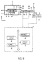
- Fig. 5 is a perspective view of the carrying arm A3
- Figs. 6A and 6B are a plan view and a side view, respectively, of the carrying arm A3.
- the carrying arm A3 has two holding forks 3 (3A and 3B), a base 31, a turning mechanism 32, linear drive mechanisms 33A and 33B, a lifting table 34, detecting units 5 (5A to 5D) and a controller 6.
- the controller 6 will be described later with reference to Figs. 8 and 9 .
- the two holding forks 3A and 3B are arranged such that the holding forks 3A and 3B can overlap each other.
- the base 31 can be turned about a vertical axis by the turning mechanism 32.
- the holding forks 3A and 3B have base end parts supported on the linear drive mechanisms 33A and 33B, respectively.
- the holding forks 3A and 3B can be advanced and retracted relative to the base 31 by the linear drive mechanisms 33A and 33B, respectively.
- the holding forks 3 correspond to the holding units of the present embodiment.
- the holding forks 3A and 3B do not necessarily need to be arranged vertically and may be horizontally arranged.
- the number of the holding forks may be one or may be three or greater.
- the plurality holding forks may be arranged either in a vertical or a horizontal arrangement.
- the linear drive mechanisms 33A and 33B are placed inside the base 31.
- a motor M shown in Fig. 9 is interlocked with the linear drive mechanisms 33A and 33B by a transmission mechanism using timing belts or the like.
- the motor M drives the linear drive mechanisms 33A and 33B to advance and retract the holding forks 3A and 3B relative to the base 31.
- the transmission mechanism may be a generally known one, such as a ball screw mechanism or a power transmission using timing belts.
- a drive mechanism 33 for driving the linear drive mechanisms 33A and 33B is disposed below the base 31.
- the motor M drives the linear drive mechanisms 33A and 33B to advance and retract the holding forks 3A and 3B relative to the base 31.
- An encoder 38 is connected to the motor M.
- a pulse counter 39 shown in Fig. 9 counts pulses generated by the encoder 38.
- the lifting table 34 lies under the turning mechanism 32.
- the lifting table 34 can be vertically moved along a straight vertical Z-axis guide rail, not shown, parallel to the Z-axis by a lifting mechanism.
- the lifting mechanism may be a generally known mechanism, such as a ball screw mechanism or a mechanism using a timing belt.
- the Z-axis guide rail and the lifting mechanism are covered with a cover 35. Upper vertical end parts of the cover 35 are connected.
- the cover 35 can slide along a straight Y-axis guide rail 36 parallel to the Y-axis.
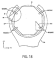
- Fig. 7 is an enlarged plan view of the holding fork 3A, in which holding protrusions 4 (4A to 4D) are enlarged relative to the holding fork 3A to facilitate illustration.
- Fig. 8 is a block diagram of the detecting units 5 and the controller 6. The controller 6 shown in Fig. 8 is identical with the controller 6 illustrated in Figs. 9 and 11 .
- the holding forks 3A and 3B are formed in a generally circular shape so as to surround a wafer W.
- the holding protrusions 4 protrude radially Inward from the Inner surface of the holding fork 3A (3B) and are arranged at equal circumferential intervals.
- a wafer W is held on the holding fork 3A (3B) with parts of the edge thereof seated on the holding protrusions 4.
- the number of the holding protrusions 4 is three or greater.
- the holding fork 3A (3B) shown in Figs. 5 and 6 is provided with four holding protrusions 4A, 4B, 4C and 4D to hold the wafer W by the four parts of the edge.
- the holding protrusions 4A to 4D are provided with suction parts 41A to 41D, respectively.
- the suction parts 41A to 41D attract the parts of the edge by vacuum suction to hold the wafer W on the holding protrusions 4A to 4D.
- the suction parts 41A to 41D has suction holes 42A to 42D formed in the holding protrusions 4A to 4D, respectively.
- the suction holes 42A to 42D connect to vacuum pipes 43A and 43B of the holding forks 3A and 3B, respectively.
- the vacuum pipe 43A (43B) is extended inside, the upper surface or the lower surface of the holding fork 3A (35) and is connected to a vacuum exhaust unit, not shown.
- the vacuum suction parts 41A to 41D thus formed can attract a wafer W by vacuum suction.
- the holding fork 3A (3B) holds a wafer W on the holding protrusions 4A to 4D by the suction parts 41A to 41D. Therefore, the holding fork 3A (3B) does not need any guide structure provided with a guide wall having a downward tapered inner surface and capable of surrounding a wafer W to guide the wafer W to a predetermined position. Therefore, when a wafer W coated with a coating film, such as a resist film, is placed on the holding fork 3A (3B), there is no possibility that the coating film coating the edge of the wafer W is abraded by the guide to produce particles.
- a coating film such as a resist film
- This embodiment can accurately measure a positional error of a wafer W on the holding fork 3A (3B) and can readily correct the positional error. Therefore, the holding fork 3A (3B) may be provided with a simple support structure Instead of the guide structure and does not necessarily need the suction parts.
- the number of the detecting units 5 (5A to 5D) is four.
- the detecting units 5 (5A to 5D) detect positions of different parts of the edge of the wafer W, respectively.
- the detecting units 5 (5A to 5D) coincide with parts of the edge of a wafer W held by the holding fork 3A (3B) in a plane.
- the detecting units 5 (5A to 5D) are arranged at angular Intervals on a circle corresponding to the edge of a wafer W held by the retracted holding fork 3A (3B).
- Each detecting unit 5 includes a light source 51 (51A, 51B, 51C or 51D) and a photodetector 52 formed by arranging a plurality of light-sensing elements.
- the photodetector 52 may be, for example, a linear image sensor 52 (52A, 52B, 52C or 52D).
- the light source 51 (51A, 51B, 51C or 51D) and the linear image sensor 52 (52A, 52B, 52C or 52D) are disposed opposite to each other on the opposite sides, respectively, of the wafer W held by the retracted holding fork 3A (3B).
- the detecting units 5A to 5D detect parts of the edge of the wafer W held by the retracted holding fork 3A (3B).
- either the light source 51 (51A to 51D) or the linear image sensor 52 (52A to 52D) is disposed below the two holding forks 3A and 3B and the other is disposed above the same.
- the light source 51 (51A to 51D) or the linear image sensor 52 (52A to 52D) is disposed below the two holding forks 3A and 3B, the light source 51 (51A to 51D) or the linear image sensor 52 (52A to 52D) may be attached to the base 31 or may be attached to the side of the lower holding fork 3B on the side of the base 31.
- the linear image sensor 52 (52A to 52D) or the linear image sensor may be attached to the base 31 or may be attached to the side of the upper holding fork 3A not facing the base 31.
- the light sources 51 are attached to the base 31 and the linear image sensors 52 are attached to the support member 53 held on the base 31.
- the detecting units 5 are thus constructed, the light sources 51 and the linear image sensors 52 can be used for detecting the positions of parts of the edge of the wafer W held by either of the holding arms 3A and 3B. Therefore, the respective numbers of the light sources 51 and the linear image sensors 52 for each of the carrying arms A1 to A4 are not large.
- detecting units 5 may be used for each of the two holding forks 3A and 3B.
- the light sources 51 and the linear image sensors 52 of each detecting unit 5 for the holding fork 3A (3B) are disposed on the opposite sides, respectively, of a wafer W held by the retracted holding fork 3A (3B).
- the number of the detecting units 5 in each of the carrying arms A1 to A4 may be greater than four.
- the light source 51 will be described on an assumption that the light source 51 is provided with an LED (light-emitting diode) or LEDs. More concretely, the light source may be a linear light source provided with a plurality of LEDs arranged on a straight line or may be a linear light source provided with a single LED and a linear light-conducting member.
- the linear image sensor 52 may be any one of linear image sensors, such as linear CCD sensors (linear charge-coupled device sensors), linear fiber sensors, photoelectric sensors and such. Image sensing elements of the linear image sensor 52 may be CCDs, photoelectric sensors or such. In the following description, the linear image sensors 52 are supposed to be linear CCD sensors.
- the detecting unit 5A has the light source 51, the linear CCD sensor 52, a linear CCD sensor control unit 54, a digital-to-analog converter (DAC) 55, and an analog-to-digital converter (ADC) 56.
- the detecting units 5B, 5C and 5D, not shown in Fig. 8 have the same configuration as the detecting unit 5A.
- the linear CCD sensor control unit 54 shifts operating times of the CCDs of the linear CCD sensor according to a clock signal generated by a clock, not shown, to move signal charges sequentially from element to element.
- the linear CCD sensor control unit 54 is a timing signal generator also.
- the linear CCD sensor control unit 54 controls current to the light source 51 also.
- the DAC 55 converts a digital control signal generated by the linear CCD sensor control unit 54 into an analog signal to be given to the light source 51.
- the ADC 56 converts an analog signal, namely, a detection signal, generated by the linear CCD sensor 52 into a digital signal to be provided by the detecting unit 5A
- the detecting unit 5 gives the detection signal conveying a detected value to the controller 6.
- the controller 6 controls, through an amplifier 57, five motors for five-axis driving, namely, X-axis drive motors M1 and M2 included in the linear drive mechanisms 33A and 33B, a Y-axis drive motor M3 installed in the base 31, a Z-axis drive motor M4 installed on the lifting table 34, and a rotational drive motor M5 included in the turning mechanism 32.
- the DAC 55 converts a control signal provided by the linear CCD sensor control unit 54 into an analog control signal and gives the analog control signal to the light source 51, and then the light source 51 shines in a bright line.
- the linear CCD sensor 52 receives light emitted by the light source 51. Charges in the linear CCD sensor 52 are moved sequentially at times according to a control signal provided by the linear CCD sensor control unit 54. Then, the linear CCD sensor 52 generates a signal conveying an amount of light received by the linear CCD sensor 52 when charges are moved.
- An output detection signal conveying a detected value provided by the linear CCD sensor 52 Is converted into a digital detection signal, by the ADC 56, and then, the digital detection signal is given to an arithmetic processing unit 61 included In the controller 6.
- the controller 6 including the arithmetic processing unit 61 measures the position of the edge of the wafer W on the basis of the digital detection signal, calculates the position of the center of the wafer W, calculates the radius of the wafer W, and decides whether or not none of the four detecting units 5A to 5D detected a notch WN formed in the wafer W. If it Is decided that one of the four detecting unit 5A to 5D detected the notch WN, the position of the holding fork 3A or 3B is corrected on the basis of detected values detected by the three detecting units 5 excluding the detecting unit that detected the notch WN.
- Heating modules 7 are components of the self units U3 of the first processing unit (DEV layer) B1, the second processing unit (BCT layer) B2, the third processing unit (COT layer) B3 and the fourth processing unit (TCT layer) B4.
- Fig. 9 shows the controller 6 in connection with the carrying arm A3 and the heating module 7 of the third processing unit (COT layer) B3.
- the heating module 7 processes a wafer W by a heating process.
- a hot plate 72 is disposed In a processing vessel 71.
- the hot plate 72 is provided with lifting pins 73.
- a lifting mechanism 74 moves the lifting pins 73 vertically.
- Indicated at 70 In Fig. 9 is a transfer opening through which a wafer W is carried into and out of the processing vessel 71.
- the controller 6 has the arithmetic processing unit 61, a storage device 62, a display 63 and an alarm generator 64.
- the arithmetic processing unit 61 Is a computer including, for example, a memory and a CPU (central processing unit).
- the arithmetic processing unit 61 reads a program stored in the storage device 62, sends control signals according to instructions included in the program to the components of the resist pattern forming system to make the resist pattern forming system execute resist pattern forming processes.
- the arithmetic processing unit 61 reads a program stored In the storage device 62, and sends control signals to the motors M1 to M5 of the carrying arm A3 according to instructions include in the program to execute transfer operations for transferring a wafer W and carrying operations for carrying a wafer W.
- the storage device 62 is a computer-adaptive storage medium storing programs to be executed by the arithmetic processing unit 61.
- the storage medium may be, for example, a flexible disk, a compact disk, a hard disk or a magnetooptical disk (MO disk).
- the display 63 Is, for example, a screen combined with a computer. Operations for selecting substrate processing processes and for entering parameters of the substrate processing processes can be achieved by operating the display 63.
- the alarm generator 64 generates an alarm when a trouble occurs in the components of the resist pattern forming system including the carrying arm A3.
- the arithmetic processing unit 61 sends predetermined control signals to the linear drive mechanisms 33A and 33B of the carrying arm A3, the motors M1 to M5 on the base 31, the lifting table 34 and the turning mechanism 32, the encoder 38 and the counter 39 to control the same.
- a program to be executed to carry out a substrate carrying method of the present embodiment is stored in the storage device 62.
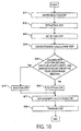
- Fig. 10 is a flow chart showing steps of the substrate carrying method.
- Figs. 11A to 11E are drawings of assistance in explaining operations of the heating module 7 and the carrying arm A3 for transferring a wafer W from the heating module 7 to the carrying arm A3.
- Fig. 12 is a graph typically showing the amounts of light received respectively by the image sensing elements of the linear image sensor.
- FIG. 13 is a plan view of a wafer W and the four linear image sensors 52A to 52D in a state in which none of the linear image sensors 52A to 52D have detected a notch WN formed in the wafer W.
- Fig. 14 is a plan view of a wafer W and the four linear image sensors 52A to 52D In a state In which the linear image sensor 52B has detected a notch WN formed In the wafer W.
- the substrate carrying method has a reception step (step S11), a retraction step (step S12), a detection step (step S13), a center-position calculation step (step S14), a decision step (step S15), a selection step (step S16 or step S16'), a displacement calculation step (step S17) and a transfer step (step S18)
- step S11 the lifting pins 73 supporting a wafer Ware raised to lift up the wafer W above the hot plate 72 by the lifting pins 73 as shown in Fig. 11A .
- the holding fork 3A is advanced from its home position along the X-axis into a space under the wafer W as shown in Fig. 11B .
- the holding fork 3A is raised as shown In Fig. 11C to receive the wafer W from the hot plate 72 of the heating module 7 by picking up the wafer W from the lifting pins 73 and holding the wafer W by the holding protrusions 4A to 4D.
- step S12 the lifting pins 73 are lowered after the wafer W has been held by the holding fork 3A. Then, the holding fork 3A is retracted along the X-axis from the heating module 7 to the home position as shown in Fig. 11E .
- step S12 the controller 6 calculates the position of the edge of the wafer W on the bases of values detected by he linear image sensors 52 after the holding fork 3A holding the wafer W has been retracted as shown in Fig. 11E .
- the light sources 51 below the holding fork 3A emit light upward after the holding form 3A holding the wafer W has been retracted to the home position in the retraction step (step S12).
- the linear image sensors 52 disposed above the holding arm 3A retracted to the home position receive the light emitted by the light source 51.
- the linear image sensors are linear CCD sensors each provided with CCDs, namely, image sensing devices, linearly arranged parallel to a diameter of the wafer W, the boundary between the CCDs that received the light and those not received the light can be determined on the basis of values measured by the CCDs.
- the boundary corresponds to a part of the edge of the wafer W.
- the horizontal position of the part of the edge of the wafer W can be measured.
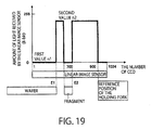
- a first value n1 Is a value detected (hereinafter, referred to as "amount of light received") by the CCDs not received the light emitted by the light source 51 and a second value n2 is an amount of light detected by the CCDs received the light emitted by the light source 51.
- a position E at the boundary of the first value n1 and the second value n2 corresponds to a part of the edge of the wafer W.
- the first value n1 can be, for example, 0 and the second value n2 can be, for example, a predetermined value not greater than 255.
- the number of the CCD at a reference position where the light emitted by the light source 51 is shaded by the holding fork 3A (3B) Is 900, which will be described later with reference to Fig. 15 .
- the LED serving as the light source 51 may be replaced by one of various kinds of light sources.
- Each of the CCDs of the linear image sensor 52 may be replaced by any of various kinds of light-receiving elements.
- an angle between a direction in which the linear image sensor 52A is extended and the Y-axis, an angle between a direction in which the linear image sensor 52B is extended and the Y-axis, an angle between a direction in which the linear image sensor 52C is extended and the Y-axis and an angle between a direction in which the linear image sensor 52D is extended and the Y-axis are angles ⁇ 1, ⁇ 2, ⁇ 3 and ⁇ 4, respectively.
- points a, b, c and d are those on the linear image sensors 52 corresponding to parts of the edge of the wafer W above the linear image sensors 52 when the wafer W is held at the reference position and points a', b', c' and d' are those on the linear image sensors 52 corresponding to the parts of the edge of the wafer W above the linear image sensors 52 when the wafer W is held by the holding fork 3A and is displaced from the reference position.
- ⁇ a, ⁇ b, ⁇ c and ⁇ d are distances between the points a and a', between the points b and b', between the points c and c' and between the points d and respectively.
- the distances ⁇ a, ⁇ b, ⁇ c and ⁇ d are expressed by Expressions (1), (2), (3) and (4).
- the coordinates (X', Y') of the center position o' namely, the position of the center of the displaced wafer W, are calculated using the coordinates of the three points out of the four points a', b', c' and d'.
- the center position o' of the center of the displaced wafer W is calculated by substituting the respective coordinates (X1', Y1'), (X2', Y2'), (X3', Y3') of the points a', b' and c' into Expression (13) and (14).
- X ⁇ X ⁇ 1 ⁇ ⁇ 2 ⁇ Y ⁇ 3 ⁇ ⁇ - Y ⁇ 2 ⁇ ⁇ + X ⁇ 2 ⁇ ⁇ 2 ⁇ Y ⁇ 1 ⁇ ⁇ - Y ⁇ 3 ⁇ ⁇ + X ⁇ 3 ⁇ ⁇ 2 ⁇ Y ⁇ 2 ⁇ ⁇ - Y ⁇ 1 ⁇ ⁇ - Y ⁇ 1 ⁇ ⁇ - Y ⁇ 3 ⁇ ⁇ ⁇ Y ⁇ 3 ⁇ ⁇ - Y ⁇ 2 ⁇ ⁇ ⁇ Y ⁇ 2 ⁇ ⁇ - Y ⁇ 1 ⁇ ⁇ 2 X ⁇ 1 ⁇ ⁇ ⁇ Y ⁇ 3 ⁇ ⁇ - Y ⁇ 2 ⁇ + X ⁇ 2 ⁇ ⁇ ⁇ ⁇ Y ⁇ 1 ⁇ ⁇ - Y ⁇ 3 ⁇ + X ⁇ 2 ⁇ ⁇ ⁇ Y ⁇ 1 ⁇ ⁇ - Y
- a radius R' is calculated by substituting the respective coordinates (X1', Y1'), (X2', Y2'), (X3', Y3') and (X', Y') of the points a', b' and c' and the center position o' into Expression (15).
- R ⁇ X ⁇ - X ⁇ 1 2 + Y ⁇ - Y ⁇ 1 2
- the coordinates (X', Y') of the center o' of the displaced wafer W are calculated by using the coordinates of combinations each of three points, such as a combination of points a', b' and d', a combination of points a', c' and d' and a combination of points b', c' and d', excluding the combination of the points a', b' and c') for use in the following decision step (step S15).
- step S15 a decision is made as to whether or not the notch WN in the edge of the wafer W has been detected by any one of the four linear image sensors 52A to 52D.
- the radius R' calculated by using the coordinates of any three points out of the points a', b', c' and d' is substantially equal to the radius R.
- the radius R' is substantially equal to the radius R, it is decided that the notch WN is not detected by any one of the four linear image sensors 52A to 52D.
- detected values detected by the three linear image sensors 52 out of the four image sensors 52A to 52D may be selected in the selection step (step S16).
- the radius R' calculated by using the coordinates of the three points out of the four points a', b', c' and d' excluding the point near the notch WN is substantially equal to the radius R as shown in Fig. 14
- the radius R' calculated by using the coordinates of the three points including the point near the notch WN is not equal to the radius R.
- it is decided that the notch WN of the wafer W is detected by one of the four linear image sensors 52A to 52D.
- the notch WN of the wafer W is near the point b' in a plane.
- detected values detected by the three linear image sensors 52 excluding the linear image sensor 52 detected the notch WN of the wafer W are selected.
- the detected values detected by the three linear image sensors 52A, 52C and 52D are selected.
- step S17 displacements ⁇ X and ⁇ Y, namely, the differences between the calculated coordinates (X', Y') of the center o' and the coordinates (X, Y) of the reference position o are calculated.
- Displacements ⁇ X and ⁇ Y are calculated by using detected values detected by the linear image sensors, namely, the linear image sensors 52A, 52C and 52D in Fig. 14 , excluding the linear image sensor detected the notch WN of the wafer W, namely, the linear image sensor 52B in Fig. 14 .
- Expressions (16) and (17) are used.
- step S18 carrying distances with respect to the X-axis and the Y-axis by which the holding fork carries the wafer W to the next processing module are adjusted by the displacements ⁇ X and ⁇ Y calculated In the displacement calculation step (step S17) such that the wafer W Is placed at a proper transfer position in the next processing module.
- step S18 the transfer position In the next processing module is corrected such that the calculated center o' coincides with the reference position o.
- the wafer W is transferred to the substrate holding device of a succeeding processing modules.
- the succeeding processing module corresponds to the succeeding processing unit of the present embodiment.
- This embodiment can accurately detect the displacement of a wafer W provided with a notch WN in its edge by the decision step (step S15) when the wafer W is held and carried, and a positional error of the displaced wafer W can be readily corrected. Even in a case where a wafer W is carried by the holding fork not provided with the guide structure, the displacement of the wafer W can be correctly measured and a positional error of the, wafer W corresponding to the displacement can be readily corrected.
- the detection step (step S13), the center-position calculation step (step S14) and the displacement calculation step (step S17) may be executed after the wafer W has been carried to the succeeding processing module to detect a displacement of the wafer W caused while the wafer W is being carried to the succeeding processing module.
- This embodiment can detect various abnormal states by using detected values, i.e., amounts of light, measured by the CCDs of the linear CCD sensors 52.
- detected values i.e., amounts of light
- Methods of detecting the abnormal bend of the holding fork 3A (3B), an abnormal state of a wafer W, an abnormal state of the light source 51 and an abnormal state of the linear CCD sensor 52 will be described.
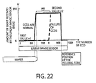
- Fig. 15 typically showing the relation between the numbers of the CCDs and the amounts of light received.
- the detecting unit 5 When the detecting unit 5 is separated from the holding forks 3A (3B), part of light emitted by the light source 51 is shaded by the holding forks 3A (3B). Detected values provided by the linear CCD sensors 52 when the partly shaded light is received by the linear CCD sensors 52 are stored beforehand. The shape of the holding forks 3A (3B) can be periodically monitored on the basis of a measured value provided by the linear CCD sensors 52 when the holding fork 3A (3B) is retracted.
- the detecting unit 5 is designed such that the position of the holding fork 3A (3B) at different positions can be detected when the holding forks 3A (3B) is retracted.
- the number of the CCD at a position where the amount of light received by the linear image sensor changes is stored as the predetermined reference position of the holding forks 3A (3B).
- the reference position of the holding fork 3A (3B) is a position where the shape of the holding forks 3A (3B) having a normal shape is detected when the holding forks 3A (3B) is retracted to its the home position.
- the number of the CCD corresponding to the reference position of the holding forks 3A (3B) Is 900.
- the number of the CCD corresponding to the reference position becomes, for example, about 700.
- the number of the CCD corresponding to the reference position changes, it is decided that the holding fork 3A (3B) is bent.
- step S18 When it is decided, on the basis of the change of the number of the CCD corresponding to the reference position, that the holding fork 3A (3B) is bent several millimeters and a carrying operation for carrying a wafer W can be continued by using the bent holding fork 3A (3B), the wafer W is carried in the transfer step (step S18), and controller 6 makes the alarm generator 64 generate an alarm upon the completion of the carrying operation. If it is decided that the bend of the holding fork 3A (3B) is extraordinarily large, the controller discontinues the carrying operation for carrying the wafer W and makes the alarm generator 64 generate an alarm.
- the controller 6 compares a position to which the holding fork 3A (3B) holding a wafer W has been retracted with the reference position of the holding fork 3A (3B) to decide whether or not the shape of the holding fork 3A (3B) is abnormal.
- the resist pattern forming system can operate at a high operating ratio. Since the position of the center of a wafer W is calculated and the bend of the carrying fork 3A (3B) is examined in every carrying cycle, breakage of the carrying fork 3A (3B) can be immediately detected.
- FIGs. 16 and 18 are enlarged plan views of the holding fork 3A holding a wafer W, in which the holding protrusions 4A, 4B, 4C and 4D and a notch WN are omitted to facilitate illustration.
- Figs. 17 and 19 are views of assistance in explaining a method of deciding that the wafer W is in an abnormal state.
- Figs. 17 and 19 typical show the relation between the number of the CCD of the linear image sensor 52 and the amount of light received by the CCD.
- the position of the edge of the wafer W can be determined by detecting the boundary between the CCD that received the first amount n1 of light and the CCD that received the second amount n2 of light. Accordingly, a state in which a wafer W is held abnormally by the holding fork 3A (3B) can be detected from the amounts of light received by the CCDs.
- a wafer W is displaced from the reference position SP and part of the wafer W juts out from the holding fork 3A and no part of the wafer W coincides with the linear image sensor 52C in a circular area I as shown in Fig. 16 .
- the amount of light received by the CCDs of the linear image sensor 52C excluding those shaded by the holding fork 3A is the second value n2 as indicated by a broken line in Fig. 17
- the amount of light received by any one of the CCDs not shaded by the holding fork 3A is not the first value n1.
- the controller 6 decides that the wafer W juts out partly from the holding fork 3A.
- the controller 6 can decide that the wafer W is broken.
- the controller 6 discontinues the carrying operation for carrying the wafer W and makes the alarm generator 64 generate an alarm.
- the controller 6 decides whether or not the wafer W is partly jutting out from the holding arm 3A (3B) and whether or not the wafer W is broken on the basis of detected values detected after the holding fork 3A (3B) holding the wafer W has been retracted. Since the center of a wafer W is calculated in every carrying cycle and the state of a wafer W can be decided, a wafer W partly jutting out from the holding arm 3A (3B) or a broken wafer W can be immediately detected.
- a method of detecting a failure of the light source 51 will be described with reference to Fig. 20 typically showing the relation between the number of the CCD of the linear image sensor 52 and the amount of light received.
- the CCDs normally not shaded by a wafer W held by the holding fork 3A receive the light. It can be decided that the light source 51 is in an abnormal state from detected values detected by those CCDs.
- the light source 51 is provided with LEDs. Possible troubles that occur in the light source 51 are, for example, burn-out of the LEDs, reduction of the luminous intensity of the LEDs, the unclean lenses combined with the LEDs and the breakage of some of cables connecting the LEDs to the controller 6.
- the controller 6 decides that a trouble occurred In the light source 51.
- the carrying operation in the transfer step (step S18) is continued to carry the wafer W.
- the controller 6 makes the alarm generator 64 generate an alarm upon the completion of the carrying operation. If the luminous intensities of the LEDs, for example, have greatly diminished and it is decided that a failure occurred in the light source 51, the controller 6 discontinues the carrying operation for carrying the wafer W and makes the alarm generator 64 generate an alarm.
- the controller 6 decides whether or not a failure occurred in the light source 51 on the basis of detected values detected by the CCDs that are not expected to be shaded from the light emitted by the light source 51 by a wafer W held by the holding fork 3A (3B).
- the resist pattern forming system can operate at a high operating ratio. Since the center of a wafer W is calculated and the state of the light source 51 can be examined in every carrying cycle, a failure of the light source 51 can be immediately found.
- Figs. 21 and 22 are graphs typically showing the relation between the number of the CCD of the linear image sensor 52 and the amount of light received by the CCD.
- the linear image sensor 52 detects the amount of light emitted by the light source 51. A decision can be made as to whether or not the light source is in an abnormal state on the basis of the detected amount of light.
- the method of detecting an abnormal state of the linear image sensor 52 similarly to the method of detecting the bend of the holding fork 3A (3B), stores beforehand a measured amount of light emitted by the light source 51 as a reference value. An abnormal state of the linear image sensor 52 can be determined on the basis of the reference value.
- a trouble such as a failure of the CCD or CCDs or breakage of some of cables connecting the linear image sensor 51 to the controller 6, occurred In the linear image sensor 52.
- the amount of light received by the CCD not shaded by a wafer W held by the light source by the holding fork 3A from light emitted by the light source does not coincide with the second value n2, which is the amount of light to be naturally measured by the CCD.
- the controller 6 decides that the linear image sensor 52 is defective if the CCD or CCDs of the linear image sensor 52 measure a value other than the second value n2 when any wafer W is not held by the holding fork 3A.
- a position E where the measured value changes from the first value n1 to the second value n2 is different from a position E0 where the measured value changes from the first value n1 to the second value n2 when the linear image sensor 52 is in a normal state; that is, the detected position of the edge of the wafer W is different from the position E0 of the same when none of the CCDs are not defective.
- the position E0 of the edge of the wafer W when the linear image sensor 52 is normal is stored beforehand and the controller 6 decides that a failure has occurred in the linear image sensor 52 when the detected position E of the edge of the wafer W is different from the stored position E0.
- the wafer W is carried in the transfer step (step S18) and the controller 6 makes the alarm generator 64 generate an alarm upon the completion of the carrying operation.
- the number of the defective CCDs is large and it is decided that the linear image sensor 52 is in an abnormal state, the operation for carrying the wafer W is discontinued and an alarm is generated,
- the controller 6 compares the reference value detected when the linear Image sensor 52 is in a norman state and a detected value detected when the holding fork 3A (3B) holding a wafer W is retracted to decide whether or not the linear image sensor 52 is in an abnormal state.
- the resist pattern forming system can operate at a high operating ratio. Since the state of the linear image sensor 52 is examined in every carrying cycle, the defective state of the linear image sensor 52 can be immediately detected.
- the linear image sensor 52 of this embodiment may be replaced by a camera and the position of a wafer W may be determined from an image formed by the camera.
- positional information about four points on the edge of a wafer W is necessary. Therefore, four cameras are not necessarily needed to obtain positional information about four points on the edge of a wafer W.
- a single camera capable of obtaining positional information about four points on the edge of a camera may be used.
- the camera may be supported above the two holding forks 3A and 3B by a support member connected to the base 31.
- a method of obtaining positional information about four points on the edge of a wafer W by using a camera forms an image of the wafer W held by the holding fork 3A (3B) retracted to the home position by the camera, and then the image formed by the camera is processed to obtain positional information about four points on the edge of the wafer W. Then, a query is made to see whether or not any one of the four points coincides with a notch WN formed in the wafer W. If any one of the four points coincides with the notch WN, the position of the holding fork 3A (3B) is adjusted on the basis of positional information about the three points excluding the positional information about the point coinciding with the notch WN.
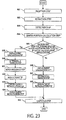
- a substrate processing method relating to a second embodiment according to the present invention will be described with reference to Figs. 23 to 25 .
- a substrate processing method relating to the second embodiment is different from the substrate processing method relating to the first embodiment in that the holding fork Is moved relative to the detecting units when any one of the detecting units detects a notch WN in a wafer W.
- the substrate processing method is carried out also by the resist pattern forming system in the first embodiment built by combining the substrate processing system and the exposure system and hence the description of the substrate processing system will be omitted.
- the substrate processing system is provided, similarly to the substrate processing system in the first embodiment, with four detecting units 5.
- the number of the necessary detecting units 5 is three or greater. Therefore, one of the four detecting units 5 may be omitted.
- Fig. 23 is a flow chart of the substrate carrying method.
- the holding fork 3A of the carrying arm A3 receives a wafer W from the heating module 7.
- the state of the heating module 7 and the carrying arm A3 is the same as that illustrated in Fig. 11 .
- a reception step (step S21), a retraction step (step S22), a detection step (step S23) and a center-position calculation step (step S24) may be considered to be the same as the reception step (step S11), the retraction step (step S12), the detection step (step S13) and the center-position calculation step (step S14) mentioned above.
- a decision step (step S25) a decision is made as to whether or not any one of the four linear image sensors 52A to 52D detected a notch WN in the edge of the wafer W.
- Fig. 24 is an enlarged plan view showing a state in which the holding fork 3A holding the wafer W and none of the linear image sensors 52A to 52D coincide with the notch WN.
- Fig. 24 it is supposed that the wafer W is held at a reference position and the center of the wafer W coincides with the center of the holding fork 3A In a plane to facilitate explanation.
- points a', b', c' and d' on the linear image sensors 52A, 52B, 52C and 52D corresponds to parts of the edge of the wafer W, respectively.
- a radius R1' calculated by using Expression (15) and positional data on the points d', a' and b' provided by the linear image sensors 52D, 52A and 52B is typically indicated by a straight line L1 with an arrow head extending from the center of the wafer W to the linear image sensor 52A.
- a radius R2' calculated by using positional data on the points a', b' and c' provided by the linear image sensors 52A, 52B and 52C is typically indicated by a straight line L2 with an arrow head extending from the center of the wafer W to the linear image sensor 52B.
- a radius R3' calculates by using positional data on the points b', c' and d' provided by the linear image sensors 52B, 52C and 52D is typically indicated by a straight line L3 with an arrow head extending from the center of the wafer W to the linear image sensor 52C.
- a radius R4' calculated by using positional data on the points c', d' and a' provide by the linear image sensors 52C, 52D and 52A is typically indicated by a straight line L4 with an arrow head extending from the center of the wafer W to the linear image sensor 52D.
- step S25 When it is decided in the decision step (step S25) that none of the four linear image sensors 52A to 52D detected the notch WN of the wafer W, a displacement calculation step (step S26), an intermodule transfer step (step S27) and a displacement recalculation step (step S28) are executed.
- the displacement calculation step (step S26) calculates, similarly to the displacement calculation step (step S17), displacement ⁇ x and ⁇ Y of the calculated center o' at o'(X', Y') from the center o of the wafer W at the reference position o(X, Y) by using Expressions (16) and (17).
- the intermodule transfer step (step S27) the carrying arm A3 whose holding fork 3A is holding the wafer W is moved from a preceding processing module to the succeeding processing module.
- Operations In the displacement recalculation step (step S28) are the same as those of the displacement calculation step (step S26).
- the displacement recalculation step (step S28) may be skipped.
- the notch WN of the wafer W coincides with one of the linear image sensors 52A to 52D in a plane.
- Fig. 25 is an enlarged plan view of the holding fork 3A holding the wafer W in a state in which one of the linear image sensors 52A to 52D coincides with the notch WN of the wafer W.
- Fig. 25 it is supposed that the wafer W is held at the reference position and the center of the wafer W coincides with the center of the holding fork 3A in a plane to facilitate explanation.
- points a', b', c' and d' on the linear image sensors 52 correspond to parts of the edge of the wafer W, respectively.
- a radius R1' calculated by using positional data on the points d', a' and b' provided by the linear image sensors 52D, 52A and 52B is typically indicated by a straight line L1 with an arrow head extending from a point near the center of the wafer W to the linear image sensor 52A.
- a radius R2' calculated by using positional data on the points a', b' and c' provided by the linear image sensors 52A, 52B and 52C is typically indicated by a straight line L2 with an arrow head extending from a point near the center of the wafer W to the linear image sensor 52B.
- a radius R3' calculated by using positional data on the points b', c' and d' provided by the linear image sensors 52B, 52C and 52D is typically Indicated by a straight line L3 with an arrow head extending from a point near the center of the wafer W to the linear image sensor 52C.
- a radius R4' calculated by using positional data on the points c', d' and a' provided by the linear image sensors 52C, 52D and 52A is typically Indicated by a straight line L4 with an arrow head extending from a point near the center of the wafer W to the linear image sensor 52D.
- Expression (15) is used for calculating the radii R1', R2', R3' and R4'.
- the radii R2' and R4' are equal to the radius R, and the radii R1' and R3' are slightly shorter than the radius R. Then, it is decided in decision step (step S25) that the notch WN of the wafer W has been detected by some of the four linear image sensors 52A to 52D.
- the radius R2' ought to be different from the radius R.
- the radius R2' is approximately equal to the radius R in some cases. It is considered that the radius R2' is approximately equal to the radius R because the radius R2' calculated by using positional data on the points a', b' and c' is equal to the radius R. Therefore, it can be decided in the decision step (step S25) that the notch WN of the wafer W has been detected by some one of the four linear image sensors 52A to 52D though, It is difficult to decide whether the notch WN is at the point b' or at the point d' in some cases.
- a displacement recalculation step (step S34) is executed after a displacement calculation step (step S29).
- Step S29 Operations in the displacement calculation step (step S29) may be similar to those in the displacement calculation step (step S26).
- an intermodule transfer step (step S30) the carrying arm A3 having the holding fork 3A holding the wafer W is moved from a preceding processing module to the succeeding processing module.
- a notch avoidance step (step S31) the holding fork 3A is moved relative to the linear image sensors 52A to 52D such that the notch WN is not detected by any one of the linear image sensors 52A to 52D. More concretely, the holding fork 3A is advanced slightly such that the coincidence of the notch WN with any one of the liner image sensors 52A to 52D is avoided.
- a distance by which the holding fork 3A is advanced in the notch avoidance step (step S31) is not shorter than a predetermined distance effective in displacing the wafer W such that none of the linear image sensors 52A to 52D detect the notch WN.
- the notch WN is a triangular depression having a depth, namely, a dimension along the diameter of the wafer W, of, for example, 1 mm and a circumferential width, namely, a dimension along the circumference of the wafer W, of, for example, 3 mm
- the predetermined distance is, for example, 4 mm.
- the displacement of the wafer W can be corrected by executing a redetection step (step S32), a center-position recalculation step (step S33) and a displacement recalculation step (step S34).
- Operations to be carried out in the redetection step (step S32), the center-position recalculation step (step S33) and the displacement recalculation step (step S34), respectively, may be similar to those to be carried out in the detection step (step S23), the center-position calculation step (step S24) and the displacement calculation step (step S26), respectively.
- the holding fork 3A is moved such that none of the linear image sensors 52A to 52D detect the notch WN in the notch avoidance step (step S31), none of the linear image sensors 52A to 52D coincide with the notch WN. Therefore, the displacements ⁇ X and ⁇ Y of the wafer W can be accurately determined by using positional data provided by the three linear image sensors out of the four linear image sensors 52A to 52D in the redetection step (step S32), the center-position recalculation step (step S33) and the displacement recalculation step (step S34).
- step S35 the wafer W is carried to the succeeding processing module in a carrying step (step S35).
- the movement of the holding fork 3A is corrected by distances respectively corresponding to the displacements ⁇ X and ⁇ Y calculated in the displacement recalculation step (step S28 or step S34) such that the wafer W can be transferred to a predetermined position, namely, a transfer position, in the succeeding processing module.
- the transfer position is corrected in the carrying step (step S35) such that the calculated center position o' coincides with the reference position o.
- displacements calculated in the displacement calculation step are not used in the carrying step (step S35) because there is the possibility that an error is made in the intermodule transfer step (step S27 or step S30) after the displacement calculation step (step S26 or step S29) has been completed and before the displacement recalculation step (step S28 or step S34) is executed. If the displacements calculated in the displacement calculation step (step S26 or step S29) and those calculated in the displacement recalculation step (step S28 or step S34) are equal, the displacements calculated in the displacement calculation step (step S26 or step S29) may be used.
- the substrate carrying operation is ended when the wafer W is transferred to the substrate support unit of the succeeding processing module after the carrying step (step S35).
- the displacement of the wafer W can be accurately measured by executing the decision step (step S25) and the notch avoidance step (step S31) even if the wafer W is provided with a notch WN and errors in the displacement can be readily corrected.
- a positional error of the displaced wafer W can be accurately measured when a holding fork not provided with the guide structure for guiding the wafer W to a predetermined position on the holding fork is used and the positional error can be readily corrected.
- the number of the detecting units 5 does not necessarily need to be four and may be three.
- the second embodiment similarly to the first embodiment, can detect the extraordinary bend of the holding fork, an abnormal state of the wafer W, malfunction of the light source and malfunction of the linear image sensor.
- the second embodiment either generates an alarm upon the completion of the carrying operation or discontinues the carrying operation and generates an alarm, depending on the degree of a trouble that occurred in the resist film forming system.
- a substrate processing method in a first modification of the second embodiment according to the present invention will be described with reference to Fig. 26 .
- the substrate processing method in this modification is different from the substrate processing method In the second embodiment in that the holding fork is moved relative to the detecting units during the intermodule transfer step in which a wafer W is moved to the succeeding processing module when any one of the detecting units detects the notch WN of the wafer W.
- a substrate processing method in this modification is the same as the substrate processing method in the first embodiment and is carried out by the resist pattern forming system built by connecting the exposure system to the coating and developing system and hence the description of the substrate processing system will be omitted.
- This modification similarly to the second embodiment, needs at least three detecting units 5 and hence one of the four detecting units 5 may be omitted.
- Fig. 26 is flow chart of a substrate carrying method.
- the substrate carrying method relating to this modification will be described on an assumption that holding fork 3A of the carrying arm A3 receives a wafer W from the heating module 7 by way of example.
- the state of the heating module 7 and the carrying arm A3 when the wafer W is transferred from the heating module 7 to the carrying arm A3 is the same as that illustrated in Figs. 11A to 11E .
- Operations in a reception step (step S41), a retraction step (step S42), a detection step (step S43), a center-position calculation step (step 544), a decision step (step S45), a displacement calculation step (step S46), an intermodule transfer step (step S47) and a displacement recalculation step (step S48) may be the same as those in the reception step (step S21), the retraction step (step S22), the detection step (step S23), the center-position calculation step (step S24), the decision step (step S25), the displacement calculation step (step S26), the intermodule transfer step (step S27) and the displacement recalculation step (step S28) of the second embodiment, respectively.
- step S50 an intermodule transfer and notch avoidance step is executed after a displacement calculation step (step S49) has been completed.
- the operation in the displacement calculation step (step S49) may be similar to that in the displacement calculation step (step S46).
- step S50 the carrying arm 3A having the holding fork 3A holding the wafer W is moved from the preceding processing module to the succeeding processing module.
- the holding fork 3A is moved relative to the linear image sensors 52A to 52D such that the notch WN is not detected by any one of the linear image sensors 52A to 52D.
- a redetection step (step S51), a center-position recalculation step (step S52) and a displacement recalculation step (step S53) are executed after the intermodule transfer and notch avoidance step (step S50).
- Step S51 Operations in the redetection step (step S51), the center-position recalculation step (step S52) and the displacement recalculation step (step S53) may be the same as those in the detection step (step S43), the center-position calculation step (step S44) and the displacement calculation step (step S46), respectively.
- step S50 Since the holding fork 3A is moved relative to the linear image sensors 52A to 52D in the intermodule transfer and notch avoidance step (step S50), the notch WN does not coincide with any one of the linear image sensors 52A to 52D. Therefore, displacements ⁇ X and ⁇ Y of the wafer W can be accurately calculated by using positional data provided by the three linear image sensors out of the four linear image sensors 52A to 52D in the redetection steps (step S51), the center-position recalculation step (step S52) and the displacement recalculation step (step S53).
- step S54 an error in a transfer position where the wafer W is transferred to the succeeding processing module is corrected such that the calculated center position o' coincides with the reference position o.
- displacements calculated in the displacement calculation step (step S46 or step S49) are not used in the carrying step (step S54) because there is the possibility that an error is made in the intermodule transfer step (step S47) or the intermodule transfer and notch avoidance step (step S50) after the displacement calculation step (step S46 or step S49) has been completed and before the displacement recalculation step (step 548 or step S53) is executed. If the displacements calculated in the displacement calculation step (step S46 or step S49) and those calculated in the displacement recalculation step (step S48 or step 553) are equal, the displacements calculated in the displacement calculation step (step S46 or step S49) may be used.
- the substrate carrying operation is ended when the wafer W is transferred to the substrate support unit of the succeeding processing module after the carrying step (step S54).
- This modification can accurately measure the displacement of a wafer W provided with a notch WN by executing the decision step (step S45) and the intermodule transfer and notch avoidance step (step S50) while the wafer W held by the holding fork is being carried and an error In the displaced wafer W can be readily corrected. Even in a case where a wafer W is carried by the holding fork not provided with the guide structure, the displacement of the wafer W can be correctly measured and a positional error of the wafer W corresponding to the displacement can be readily corrected.
- the number of the detecting units 5 is not necessarily four and may be three.
- This modification similarly to the first embodiment, can detect the extraordinary bend of the holding fork, an abnormal state of a wafer W, malfunction of the light source and malfunction of the linear image sensor. This modification either generates an alarm upon the completion of the carrying operation or discontinues the carrying operation and generates an alarm, depending on the degree of a trouble that occurred In the resist film forming system.
- a substrate processing method in a second modification of the second embodiment will be described with reference to Fig. 27 .
- the substrate processing method in the second modification differs from the substrate processing method in the second embodiment in that displacements of a wafer W is measured again after the wafer W has been carried to the succeeding processing module.
- the substrate processing method in this modification Is the same as the substrate processing method in the first embodiment and is carried out by the resist pattern forming system built by connecting the exposure system to the coating and developing system and hence the description of the substrate processing system will be omitted.
- This modification similarly to the second embodiment, needs at least three detecting units 5 and hence one of the four detecting units 5 may be omitted.
- Fig. 27 is a flow chart of a substrate carrying method.
- the substrate carrying method In this modification will be described on an assumption that the holding fork 3A of the carrying arm A3 receives a wafer W from the heating module 7 by way of example.
- the state of the heating module 7 and the carrying arm A3 when the wafer W is transferred from the heating module 7 to the carrying arm A3 is the same as that Illustrated in Figs. 11A to 11E .
- a third detection step (step S72), a third center-position calculation step (step S73), a third displacement calculation step (step S74) and a carrying step (step S75) are executed after the intermodule transfer step (step S71).
- Operations In the third detection step (step S72), the third center-position calculation step (step S73) and the third displacement calculation step (step S74) are the same as those in the detection step (step S63), the center-position calculation step (step S64) and the displacement calculation step (step S66), respectively.
- displacements by which the wafer W is moved during the transfer of the wafer W to the succeeding processing module can be measured after displacements have been measured for the first time in the displacement calculation step (step S66) or the second displacement calculation step (step S70).
- step S75 In the carrying step (step S75) following the third displacement calculation step (step S74), an error in a transfer position where the wafer W is transferred to the succeeding processing module such that a calculated center position o' coincides with the reference position o.
- displacements calculated in the displacement calculation step (step S66) are not used in the carrying step (step S75) because there is the possibility that an error is made in the intermodule transfer step (step S71) after the displacement calculation step (step S66) has been completed and before the third displacement calculation step (step S74) is executed. If the displacements calculated in the displacement calculation step (step S66) and those calculated in the third displacement calculation step (step S74) are equal, the displacements calculated in the displacement calculation step (step S66) may be used.
- the substrate carrying operation is ended when the wafer W is transferred to the substrate support unit of the succeeding processing module after the carrying step (step S75).
- the displacement of the wafer W can be accurately measured by executing the decision step (step S65) and the notch avoidance step (step S67) even if a wafer W is provided with a notch WN and errors in the displacements can be readily corrected.
- a positional error of the displaced wafer W can be accurately measured when the holding fork not provided with the guide structure for guiding the wafer W to a predetermined position on the holding fork is used and the positional error can be readily corrected.
- the notch avoidance step (step S67) may be executed by using the three detecting units out of the four detecting units 5.
- This modification similarly to the first embodiment, can detect the extraordinary bend of the holding fork, an abnormal state of the wafer W, malfunction of the light source and malfunction of the linear image sensor. This modification either generates an alarm upon the completion of the carrying operation or discontinues the carrying operation and generates an alarm, depending on the degree of a trouble.
Landscapes
- Engineering & Computer Science (AREA)
- Manufacturing & Machinery (AREA)
- Computer Hardware Design (AREA)
- Microelectronics & Electronic Packaging (AREA)
- Power Engineering (AREA)
- Physics & Mathematics (AREA)
- Condensed Matter Physics & Semiconductors (AREA)
- General Physics & Mathematics (AREA)
- Robotics (AREA)
- Container, Conveyance, Adherence, Positioning, Of Wafer (AREA)
- Exposure Of Semiconductors, Excluding Electron Or Ion Beam Exposure (AREA)
Applications Claiming Priority (2)
| Application Number | Priority Date | Filing Date | Title |
|---|---|---|---|
| JP2010185068 | 2010-08-20 | ||
| JP2011037159A JP5614326B2 (ja) | 2010-08-20 | 2011-02-23 | 基板搬送装置、基板搬送方法及びその基板搬送方法を実行させるためのプログラムを記録した記録媒体 |
Publications (3)
| Publication Number | Publication Date |
|---|---|
| EP2421034A2 EP2421034A2 (en) | 2012-02-22 |
| EP2421034A3 EP2421034A3 (en) | 2012-06-20 |
| EP2421034B1 true EP2421034B1 (en) | 2014-01-22 |
Family
ID=44735825
Family Applications (1)
| Application Number | Title | Priority Date | Filing Date |
|---|---|---|---|
| EP11178081.3A Active EP2421034B1 (en) | 2010-08-20 | 2011-08-19 | Substrate carrying mechanism and substrate carrying method |
Country Status (7)
| Country | Link |
|---|---|
| US (1) | US8781787B2 (zh) |
| EP (1) | EP2421034B1 (zh) |
| JP (1) | JP5614326B2 (zh) |
| KR (5) | KR101524335B1 (zh) |
| CN (2) | CN104867856B (zh) |
| SG (1) | SG178699A1 (zh) |
| TW (3) | TWI521636B (zh) |
Families Citing this family (40)
| Publication number | Priority date | Publication date | Assignee | Title |
|---|---|---|---|---|
| JP5333408B2 (ja) * | 2010-10-22 | 2013-11-06 | 東京エレクトロン株式会社 | 保持部材の姿勢判定装置、その方法、基板処理装置及び記憶媒体 |
| JP5582152B2 (ja) | 2012-02-03 | 2014-09-03 | 東京エレクトロン株式会社 | 基板搬送装置、基板搬送方法及び記憶媒体 |
| JP5884624B2 (ja) * | 2012-05-02 | 2016-03-15 | 東京エレクトロン株式会社 | 基板処理装置、調整方法及び記憶媒体 |
| KR102044788B1 (ko) * | 2012-10-30 | 2019-11-18 | 삼성디스플레이 주식회사 | 글라스 기판 검사 장치 |
| ITMO20130088A1 (it) | 2013-04-05 | 2014-10-06 | Kemet Electronics Italia S R L | Sistema di movimentazione |
| US9088508B1 (en) | 2014-04-11 | 2015-07-21 | Level 3 Communications, Llc | Incremental application of resources to network traffic flows based on heuristics and business policies |
| JP6316742B2 (ja) | 2014-12-24 | 2018-04-25 | 東京エレクトロン株式会社 | 基板搬送装置および基板搬送方法 |
| CN104690736B (zh) * | 2015-02-12 | 2017-03-08 | 成都天马微电子有限公司 | 机械手臂及其检测系统和检测方法 |
| CN104708632B (zh) * | 2015-03-27 | 2017-03-22 | 河北工业大学 | 板材搬运安装机械手控制系统 |
| JP6311639B2 (ja) * | 2015-04-13 | 2018-04-18 | 東京エレクトロン株式会社 | 基板処理装置、基板処理装置の運転方法及び記憶媒体 |
| JP6463227B2 (ja) * | 2015-07-07 | 2019-01-30 | 東京エレクトロン株式会社 | 基板搬送方法 |
| KR101757815B1 (ko) | 2015-09-25 | 2017-07-14 | 세메스 주식회사 | 기판 중심 검출 방법, 기판 반송 방법, 반송 유닛 및 이를 포함하는 기판 처리 장치. |
| US9978631B2 (en) * | 2015-12-31 | 2018-05-22 | Beijing Naura Microelectronics Equipment Co., Ltd. | Wafer pick-and-place method and system |
| CN107452641B (zh) * | 2016-05-31 | 2020-10-23 | 细美事有限公司 | 从晶圆上拾取裸芯的方法 |
| JP6617649B2 (ja) * | 2016-06-20 | 2019-12-11 | 東京エレクトロン株式会社 | 被処理基板の載置位置の設定方法及び成膜システム |
| CN106098580A (zh) * | 2016-06-29 | 2016-11-09 | 昆山国显光电有限公司 | 一种液帘分叉检测装置及方法 |
| KR102066044B1 (ko) * | 2016-06-30 | 2020-02-11 | 세메스 주식회사 | 기판 처리 장치, 인덱스 로봇 및 기판 이송 방법 |
| JP6635888B2 (ja) * | 2016-07-14 | 2020-01-29 | 東京エレクトロン株式会社 | プラズマ処理システム |
| JP6723131B2 (ja) * | 2016-09-29 | 2020-07-15 | 株式会社Screenホールディングス | 基板搬送装置および基板搬送方法 |
| CN106783705B (zh) * | 2016-11-30 | 2019-05-14 | 上海华力微电子有限公司 | 一种用于优化晶圆边缘缺陷的晶圆传送方法 |
| JP6842934B2 (ja) * | 2017-01-27 | 2021-03-17 | 株式会社Screenホールディングス | 基板搬送装置、検出位置較正方法および基板処理装置 |
| JP6802726B2 (ja) | 2017-02-14 | 2020-12-16 | 株式会社Screenホールディングス | 基板搬送装置、それを備える基板処理装置および基板搬送方法 |
| JP6862903B2 (ja) | 2017-02-23 | 2021-04-21 | 東京エレクトロン株式会社 | 基板搬送装置、基板搬送方法及び記憶媒体 |
| JP6276449B1 (ja) * | 2017-03-30 | 2018-02-07 | 株式会社荏原製作所 | 基板処理装置、基板処理装置の制御方法、プログラムを格納した記憶媒体 |
| JP2019067948A (ja) * | 2017-10-02 | 2019-04-25 | 川崎重工業株式会社 | 基板搬送装置 |
| JP7030497B2 (ja) * | 2017-12-13 | 2022-03-07 | 株式会社荏原製作所 | 基板処理装置、基板処理装置の制御方法、プログラムを格納した記憶媒体 |
| JP6458292B2 (ja) * | 2018-03-19 | 2019-01-30 | 東京エレクトロン株式会社 | 基板処理装置、基板処理装置の運転方法及び記憶媒体 |
| KR102099115B1 (ko) * | 2018-06-08 | 2020-04-10 | 세메스 주식회사 | 기판 이송 장치, 이를 포함하는 기판 처리 장치 및 기판 틀어짐 보정 방법 |
| US11587807B2 (en) | 2018-10-28 | 2023-02-21 | Taiwan Semiconductor Manufacturing Co., Ltd. | Annealing apparatus and method thereof |
| KR102225937B1 (ko) | 2019-07-01 | 2021-03-10 | 세메스 주식회사 | 기판 반송 장치 및 이를 구비하는 기판 처리 시스템 |
| CN110580692B (zh) * | 2019-09-11 | 2022-03-25 | 北京空间飞行器总体设计部 | 一种多线列时差扫描图像辐射一致性校正方法 |
| JP2021048322A (ja) * | 2019-09-19 | 2021-03-25 | 株式会社Screenホールディングス | 基板搬送装置および基板搬送方法 |
| KR20210039523A (ko) * | 2019-10-01 | 2021-04-12 | 삼성전자주식회사 | 웨이퍼 이송 장치 및 이를 이용한 웨이퍼 이송 방법 |
| JP7357549B2 (ja) * | 2020-01-07 | 2023-10-06 | 東京エレクトロン株式会社 | 基板の位置ずれ検出方法、基板位置の異常判定方法、基板搬送制御方法、及び基板の位置ずれ検出装置 |
| US11435391B2 (en) | 2020-01-22 | 2022-09-06 | Nanya Technology Corporation | Dual-sided wafer imaging apparatus and methods thereof |
| JP2022002255A (ja) * | 2020-06-19 | 2022-01-06 | 東京エレクトロン株式会社 | 収納モジュール、基板処理システムおよび消耗部材の搬送方法 |
| US11600504B2 (en) | 2020-06-29 | 2023-03-07 | Taiwan Semiconductor Manufacturing Company, Ltd. | Detecting damaged semiconductor wafers utilizing a semiconductor wafer sorter tool of an automated materials handling system |
| KR102624577B1 (ko) | 2020-10-28 | 2024-01-15 | 세메스 주식회사 | 기판 처리 장치 및 기판 처리 방법 |
| KR20240025790A (ko) | 2022-08-19 | 2024-02-27 | 세메스 주식회사 | 기판 이송 유닛 |
| CN117576092B (zh) * | 2024-01-15 | 2024-03-29 | 成都瑞迪威科技有限公司 | 一种基于图像处理的晶圆元器件统计方法 |
Family Cites Families (36)
| Publication number | Priority date | Publication date | Assignee | Title |
|---|---|---|---|---|
| EP0597637B1 (en) * | 1992-11-12 | 2000-08-23 | Applied Materials, Inc. | System and method for automated positioning of a substrate in a processing chamber |
| US6225012B1 (en) * | 1994-02-22 | 2001-05-01 | Nikon Corporation | Method for positioning substrate |
| JPH0831905A (ja) * | 1994-07-19 | 1996-02-02 | Hitachi Ltd | 半導体製造装置 |
| JP4128254B2 (ja) | 1998-02-25 | 2008-07-30 | オリンパス株式会社 | 半導体ウエハ位置検出装置および検査装置 |
| JP2000071190A (ja) * | 1998-08-27 | 2000-03-07 | Komatsu Ltd | ワーク搬送システム |
| JP2000100895A (ja) * | 1998-09-18 | 2000-04-07 | Nikon Corp | 基板の搬送装置、基板の保持装置、及び基板処理装置 |
| US6298280B1 (en) * | 1998-09-28 | 2001-10-02 | Asyst Technologies, Inc. | Method for in-cassette wafer center determination |
| US6405101B1 (en) * | 1998-11-17 | 2002-06-11 | Novellus Systems, Inc. | Wafer centering system and method |
| JP2001038614A (ja) * | 1999-07-26 | 2001-02-13 | Ebara Corp | 研磨装置 |
| JP2001237294A (ja) * | 2000-02-23 | 2001-08-31 | Tatsumo Kk | 特定環境用ロボット |
| JP4402811B2 (ja) * | 2000-05-26 | 2010-01-20 | 東京エレクトロン株式会社 | 被処理体の搬送システムおよび被処理体の位置ずれ量の検出方法 |
| TW559855B (en) | 2000-09-06 | 2003-11-01 | Olympus Optical Co | Wafer transfer apparatus |
| JP2002261146A (ja) * | 2001-03-02 | 2002-09-13 | Hitachi Ltd | 半導体集積回路装置の製造方法および半導体製造装置 |
| JP2002319612A (ja) * | 2001-04-20 | 2002-10-31 | Shin Etsu Handotai Co Ltd | ウェーハ搬送装置、気相成長装置およびウェーハ搬送方法 |
| JP3795820B2 (ja) * | 2002-03-27 | 2006-07-12 | 株式会社東芝 | 基板のアライメント装置 |
| US7988398B2 (en) * | 2002-07-22 | 2011-08-02 | Brooks Automation, Inc. | Linear substrate transport apparatus |
| US7019817B2 (en) * | 2003-07-14 | 2006-03-28 | Kawasaki Jukogyo Kabuishiki Kaisha | Edge-holding aligner |
| JP4289961B2 (ja) * | 2003-09-26 | 2009-07-01 | キヤノン株式会社 | 位置決め装置 |
| US20050113964A1 (en) | 2003-11-10 | 2005-05-26 | Blueshift Technologies, Inc. | Sensor methods and systems for semiconductor handling |
| JPWO2006025386A1 (ja) * | 2004-08-31 | 2008-05-08 | 株式会社ニコン | 位置合わせ方法、処理システム、基板の投入再現性計測方法、位置計測方法、露光方法、基板処理装置、計測方法及び計測装置 |
| KR20060088817A (ko) * | 2005-01-28 | 2006-08-07 | 가부시키가이샤 이빔 | 기판처리장치 및 기판처리방법 |
| JP2006351884A (ja) * | 2005-06-16 | 2006-12-28 | Tokyo Electron Ltd | 基板搬送機構及び処理システム |
| JP4698407B2 (ja) * | 2005-12-20 | 2011-06-08 | 大日本スクリーン製造株式会社 | 基板処理装置および基板処理方法 |
| JP5132108B2 (ja) * | 2006-02-02 | 2013-01-30 | 株式会社Sokudo | 基板処理装置 |
| US7480050B2 (en) * | 2006-02-09 | 2009-01-20 | Asml Netherlands B.V. | Lithographic system, sensor, and method of measuring properties of a substrate |
| US8101934B2 (en) * | 2006-03-07 | 2012-01-24 | Applied Materials, Inc. | Methods and apparatus for detecting a substrate notch or flat |
| JP2007335613A (ja) * | 2006-06-15 | 2007-12-27 | Nikon Corp | 基板位置検出装置、基板搬送装置、露光装置、基板位置検出方法及びマイクロデバイスの製造方法 |
| US8057153B2 (en) | 2006-09-05 | 2011-11-15 | Tokyo Electron Limited | Substrate transfer device, substrate processing apparatus and substrate transfer method |
| JP4799325B2 (ja) * | 2006-09-05 | 2011-10-26 | 東京エレクトロン株式会社 | 基板受け渡し装置,基板処理装置,基板受け渡し方法 |
| JP4607848B2 (ja) * | 2006-10-27 | 2011-01-05 | 東京エレクトロン株式会社 | 基板処理装置、基板受け渡し位置の調整方法及び記憶媒体 |
| US8057602B2 (en) * | 2007-05-09 | 2011-11-15 | Applied Materials, Inc. | Apparatus and method for supporting, positioning and rotating a substrate in a processing chamber |
| JP4956328B2 (ja) * | 2007-08-24 | 2012-06-20 | 東京エレクトロン株式会社 | 搬送アームの移動位置の調整方法及び位置検出用治具 |
| JP2009071008A (ja) * | 2007-09-13 | 2009-04-02 | Sokudo:Kk | 基板処理装置 |
| NL1036025A1 (nl) * | 2007-10-10 | 2009-04-15 | Asml Netherlands Bv | Method of transferring a substrate, transfer system and lithographic projection apparatus. |
| US8639524B2 (en) * | 2008-08-08 | 2014-01-28 | Neal Solomon | System for intelligent medical device network |
| JP5185756B2 (ja) * | 2008-10-01 | 2013-04-17 | 川崎重工業株式会社 | 基板検出装置および方法 |
-
2011
- 2011-02-23 JP JP2011037159A patent/JP5614326B2/ja active Active
- 2011-07-06 KR KR1020110066928A patent/KR101524335B1/ko active IP Right Review Request
- 2011-08-11 TW TW103140083A patent/TWI521636B/zh active
- 2011-08-11 TW TW100128779A patent/TWI475634B/zh active
- 2011-08-11 TW TW104143256A patent/TWI574343B/zh active
- 2011-08-19 US US13/213,445 patent/US8781787B2/en active Active
- 2011-08-19 CN CN201510246746.5A patent/CN104867856B/zh active Active
- 2011-08-19 EP EP11178081.3A patent/EP2421034B1/en active Active
- 2011-08-19 CN CN201110242600.5A patent/CN102376612B/zh active Active
- 2011-08-19 SG SG2011060571A patent/SG178699A1/en unknown
-
2014
- 2014-10-22 KR KR1020140143481A patent/KR101601510B1/ko active IP Right Grant
-
2016
- 2016-02-25 KR KR1020160022561A patent/KR101790867B1/ko active IP Right Review Request
-
2017
- 2017-10-18 KR KR1020170135134A patent/KR101891446B1/ko active IP Right Grant
-
2018
- 2018-08-10 KR KR1020180093820A patent/KR101931061B1/ko active IP Right Grant
Also Published As
| Publication number | Publication date |
|---|---|
| KR101790867B1 (ko) | 2017-10-26 |
| KR20140130094A (ko) | 2014-11-07 |
| JP2012064918A (ja) | 2012-03-29 |
| US8781787B2 (en) | 2014-07-15 |
| KR101931061B1 (ko) | 2018-12-19 |
| KR20180094505A (ko) | 2018-08-23 |
| KR20160030143A (ko) | 2016-03-16 |
| JP5614326B2 (ja) | 2014-10-29 |
| TWI475634B (zh) | 2015-03-01 |
| CN104867856B (zh) | 2017-11-24 |
| KR101524335B1 (ko) | 2015-05-29 |
| KR101601510B1 (ko) | 2016-03-11 |
| KR20120023517A (ko) | 2012-03-13 |
| TW201508858A (zh) | 2015-03-01 |
| US20120046904A1 (en) | 2012-02-23 |
| KR101790867B9 (ko) | 2021-10-15 |
| TW201616597A (zh) | 2016-05-01 |
| TW201230240A (en) | 2012-07-16 |
| CN104867856A (zh) | 2015-08-26 |
| CN102376612A (zh) | 2012-03-14 |
| TWI521636B (zh) | 2016-02-11 |
| TWI574343B (zh) | 2017-03-11 |
| CN102376612B (zh) | 2015-06-17 |
| EP2421034A2 (en) | 2012-02-22 |
| SG178699A1 (en) | 2012-03-29 |
| EP2421034A3 (en) | 2012-06-20 |
| KR101891446B1 (ko) | 2018-08-24 |
| KR20170121729A (ko) | 2017-11-02 |
Similar Documents
| Publication | Publication Date | Title |
|---|---|---|
| EP2421034B1 (en) | Substrate carrying mechanism and substrate carrying method | |
| KR101485297B1 (ko) | 열처리 장치 및 기판 반송 위치 조정 방법 | |
| US7248931B2 (en) | Semiconductor wafer position shift measurement and correction | |
| KR101015778B1 (ko) | 기판 처리장치 및 기판 수수 위치의 조정 방법 | |
| TWI517287B (zh) | 基板運送裝置、基板運送方法及記錄媒體 | |
| JP2015119070A (ja) | ロボットシステム及び検出方法 | |
| JP5733437B2 (ja) | 基板搬送装置、基板搬送方法及び記録媒体 | |
| JP2009184069A (ja) | ウエハ搬送装置及びその調整方法 | |
| WO2024080332A1 (ja) | 基板搬送ロボットシステム | |
| KR20220133107A (ko) | 기판 처리 장치, 교시 정보 생성 방법, 교시 세트 및 기판형 지그 |
Legal Events
| Date | Code | Title | Description |
|---|---|---|---|
| AK | Designated contracting states |
Kind code of ref document: A2 Designated state(s): AL AT BE BG CH CY CZ DE DK EE ES FI FR GB GR HR HU IE IS IT LI LT LU LV MC MK MT NL NO PL PT RO RS SE SI SK SM TR |
|
| AX | Request for extension of the european patent |
Extension state: BA ME |
|
| PUAI | Public reference made under article 153(3) epc to a published international application that has entered the european phase |
Free format text: ORIGINAL CODE: 0009012 |
|
| PUAL | Search report despatched |
Free format text: ORIGINAL CODE: 0009013 |
|
| AK | Designated contracting states |
Kind code of ref document: A3 Designated state(s): AL AT BE BG CH CY CZ DE DK EE ES FI FR GB GR HR HU IE IS IT LI LT LU LV MC MK MT NL NO PL PT RO RS SE SI SK SM TR |
|
| AX | Request for extension of the european patent |
Extension state: BA ME |
|
| RIC1 | Information provided on ipc code assigned before grant |
Ipc: H01L 21/68 20060101AFI20120514BHEP |
|
| 17P | Request for examination filed |
Effective date: 20121017 |
|
| 17Q | First examination report despatched |
Effective date: 20130212 |
|
| GRAP | Despatch of communication of intention to grant a patent |
Free format text: ORIGINAL CODE: EPIDOSNIGR1 |
|
| INTG | Intention to grant announced |
Effective date: 20130903 |
|
| RIN1 | Information on inventor provided before grant (corrected) |
Inventor name: SAKAGUCHI, KIMINARI Inventor name: HAYASHI, TOKUTAROU |
|
| GRAS | Grant fee paid |
Free format text: ORIGINAL CODE: EPIDOSNIGR3 |
|
| GRAA | (expected) grant |
Free format text: ORIGINAL CODE: 0009210 |
|
| AK | Designated contracting states |
Kind code of ref document: B1 Designated state(s): AL AT BE BG CH CY CZ DE DK EE ES FI FR GB GR HR HU IE IS IT LI LT LU LV MC MK MT NL NO PL PT RO RS SE SI SK SM TR |
|
| REG | Reference to a national code |
Ref country code: GB Ref legal event code: FG4D |
|
| REG | Reference to a national code |
Ref country code: CH Ref legal event code: EP |
|
| REG | Reference to a national code |
Ref country code: AT Ref legal event code: REF Ref document number: 651127 Country of ref document: AT Kind code of ref document: T Effective date: 20140215 |
|
| REG | Reference to a national code |
Ref country code: IE Ref legal event code: FG4D |
|
| REG | Reference to a national code |
Ref country code: DE Ref legal event code: R096 Ref document number: 602011004770 Country of ref document: DE Effective date: 20140306 |
|
| REG | Reference to a national code |
Ref country code: NL Ref legal event code: VDEP Effective date: 20140122 |
|
| REG | Reference to a national code |
Ref country code: AT Ref legal event code: MK05 Ref document number: 651127 Country of ref document: AT Kind code of ref document: T Effective date: 20140122 |
|
| REG | Reference to a national code |
Ref country code: LT Ref legal event code: MG4D |
|
| PG25 | Lapsed in a contracting state [announced via postgrant information from national office to epo] |
Ref country code: NO Free format text: LAPSE BECAUSE OF FAILURE TO SUBMIT A TRANSLATION OF THE DESCRIPTION OR TO PAY THE FEE WITHIN THE PRESCRIBED TIME-LIMIT Effective date: 20140422 Ref country code: LT Free format text: LAPSE BECAUSE OF FAILURE TO SUBMIT A TRANSLATION OF THE DESCRIPTION OR TO PAY THE FEE WITHIN THE PRESCRIBED TIME-LIMIT Effective date: 20140122 Ref country code: IS Free format text: LAPSE BECAUSE OF FAILURE TO SUBMIT A TRANSLATION OF THE DESCRIPTION OR TO PAY THE FEE WITHIN THE PRESCRIBED TIME-LIMIT Effective date: 20140522 |
|
| PG25 | Lapsed in a contracting state [announced via postgrant information from national office to epo] |
Ref country code: FI Free format text: LAPSE BECAUSE OF FAILURE TO SUBMIT A TRANSLATION OF THE DESCRIPTION OR TO PAY THE FEE WITHIN THE PRESCRIBED TIME-LIMIT Effective date: 20140122 Ref country code: SE Free format text: LAPSE BECAUSE OF FAILURE TO SUBMIT A TRANSLATION OF THE DESCRIPTION OR TO PAY THE FEE WITHIN THE PRESCRIBED TIME-LIMIT Effective date: 20140122 Ref country code: AT Free format text: LAPSE BECAUSE OF FAILURE TO SUBMIT A TRANSLATION OF THE DESCRIPTION OR TO PAY THE FEE WITHIN THE PRESCRIBED TIME-LIMIT Effective date: 20140122 Ref country code: CY Free format text: LAPSE BECAUSE OF FAILURE TO SUBMIT A TRANSLATION OF THE DESCRIPTION OR TO PAY THE FEE WITHIN THE PRESCRIBED TIME-LIMIT Effective date: 20140122 Ref country code: ES Free format text: LAPSE BECAUSE OF FAILURE TO SUBMIT A TRANSLATION OF THE DESCRIPTION OR TO PAY THE FEE WITHIN THE PRESCRIBED TIME-LIMIT Effective date: 20140122 Ref country code: PT Free format text: LAPSE BECAUSE OF FAILURE TO SUBMIT A TRANSLATION OF THE DESCRIPTION OR TO PAY THE FEE WITHIN THE PRESCRIBED TIME-LIMIT Effective date: 20140522 Ref country code: NL Free format text: LAPSE BECAUSE OF FAILURE TO SUBMIT A TRANSLATION OF THE DESCRIPTION OR TO PAY THE FEE WITHIN THE PRESCRIBED TIME-LIMIT Effective date: 20140122 |
|
| PG25 | Lapsed in a contracting state [announced via postgrant information from national office to epo] |
Ref country code: HR Free format text: LAPSE BECAUSE OF FAILURE TO SUBMIT A TRANSLATION OF THE DESCRIPTION OR TO PAY THE FEE WITHIN THE PRESCRIBED TIME-LIMIT Effective date: 20140122 Ref country code: LV Free format text: LAPSE BECAUSE OF FAILURE TO SUBMIT A TRANSLATION OF THE DESCRIPTION OR TO PAY THE FEE WITHIN THE PRESCRIBED TIME-LIMIT Effective date: 20140122 Ref country code: BE Free format text: LAPSE BECAUSE OF FAILURE TO SUBMIT A TRANSLATION OF THE DESCRIPTION OR TO PAY THE FEE WITHIN THE PRESCRIBED TIME-LIMIT Effective date: 20140122 Ref country code: RS Free format text: LAPSE BECAUSE OF FAILURE TO SUBMIT A TRANSLATION OF THE DESCRIPTION OR TO PAY THE FEE WITHIN THE PRESCRIBED TIME-LIMIT Effective date: 20140122 |
|
| REG | Reference to a national code |
Ref country code: DE Ref legal event code: R097 Ref document number: 602011004770 Country of ref document: DE |
|
| PG25 | Lapsed in a contracting state [announced via postgrant information from national office to epo] |
Ref country code: DK Free format text: LAPSE BECAUSE OF FAILURE TO SUBMIT A TRANSLATION OF THE DESCRIPTION OR TO PAY THE FEE WITHIN THE PRESCRIBED TIME-LIMIT Effective date: 20140122 Ref country code: CZ Free format text: LAPSE BECAUSE OF FAILURE TO SUBMIT A TRANSLATION OF THE DESCRIPTION OR TO PAY THE FEE WITHIN THE PRESCRIBED TIME-LIMIT Effective date: 20140122 Ref country code: RO Free format text: LAPSE BECAUSE OF FAILURE TO SUBMIT A TRANSLATION OF THE DESCRIPTION OR TO PAY THE FEE WITHIN THE PRESCRIBED TIME-LIMIT Effective date: 20140122 Ref country code: EE Free format text: LAPSE BECAUSE OF FAILURE TO SUBMIT A TRANSLATION OF THE DESCRIPTION OR TO PAY THE FEE WITHIN THE PRESCRIBED TIME-LIMIT Effective date: 20140122 |
|
| PG25 | Lapsed in a contracting state [announced via postgrant information from national office to epo] |
Ref country code: PL Free format text: LAPSE BECAUSE OF FAILURE TO SUBMIT A TRANSLATION OF THE DESCRIPTION OR TO PAY THE FEE WITHIN THE PRESCRIBED TIME-LIMIT Effective date: 20140122 Ref country code: SK Free format text: LAPSE BECAUSE OF FAILURE TO SUBMIT A TRANSLATION OF THE DESCRIPTION OR TO PAY THE FEE WITHIN THE PRESCRIBED TIME-LIMIT Effective date: 20140122 |
|
| PLBE | No opposition filed within time limit |
Free format text: ORIGINAL CODE: 0009261 |
|
| STAA | Information on the status of an ep patent application or granted ep patent |
Free format text: STATUS: NO OPPOSITION FILED WITHIN TIME LIMIT |
|
| 26N | No opposition filed |
Effective date: 20141023 |
|
| REG | Reference to a national code |
Ref country code: DE Ref legal event code: R097 Ref document number: 602011004770 Country of ref document: DE Effective date: 20141023 |
|
| PG25 | Lapsed in a contracting state [announced via postgrant information from national office to epo] |
Ref country code: LU Free format text: LAPSE BECAUSE OF FAILURE TO SUBMIT A TRANSLATION OF THE DESCRIPTION OR TO PAY THE FEE WITHIN THE PRESCRIBED TIME-LIMIT Effective date: 20140819 Ref country code: MC Free format text: LAPSE BECAUSE OF FAILURE TO SUBMIT A TRANSLATION OF THE DESCRIPTION OR TO PAY THE FEE WITHIN THE PRESCRIBED TIME-LIMIT Effective date: 20140122 |
|
| REG | Reference to a national code |
Ref country code: CH Ref legal event code: PL |
|
| PG25 | Lapsed in a contracting state [announced via postgrant information from national office to epo] |
Ref country code: LI Free format text: LAPSE BECAUSE OF NON-PAYMENT OF DUE FEES Effective date: 20140831 Ref country code: CH Free format text: LAPSE BECAUSE OF NON-PAYMENT OF DUE FEES Effective date: 20140831 |
|
| REG | Reference to a national code |
Ref country code: IE Ref legal event code: MM4A |
|
| PG25 | Lapsed in a contracting state [announced via postgrant information from national office to epo] |
Ref country code: SI Free format text: LAPSE BECAUSE OF FAILURE TO SUBMIT A TRANSLATION OF THE DESCRIPTION OR TO PAY THE FEE WITHIN THE PRESCRIBED TIME-LIMIT Effective date: 20140122 |
|
| REG | Reference to a national code |
Ref country code: FR Ref legal event code: ST Effective date: 20150430 |
|
| PG25 | Lapsed in a contracting state [announced via postgrant information from national office to epo] |
Ref country code: FR Free format text: LAPSE BECAUSE OF NON-PAYMENT OF DUE FEES Effective date: 20140901 Ref country code: IE Free format text: LAPSE BECAUSE OF NON-PAYMENT OF DUE FEES Effective date: 20140819 |
|
| GBPC | Gb: european patent ceased through non-payment of renewal fee |
Effective date: 20150819 |
|
| PG25 | Lapsed in a contracting state [announced via postgrant information from national office to epo] |
Ref country code: SM Free format text: LAPSE BECAUSE OF FAILURE TO SUBMIT A TRANSLATION OF THE DESCRIPTION OR TO PAY THE FEE WITHIN THE PRESCRIBED TIME-LIMIT Effective date: 20140122 |
|
| PG25 | Lapsed in a contracting state [announced via postgrant information from national office to epo] |
Ref country code: IT Free format text: LAPSE BECAUSE OF FAILURE TO SUBMIT A TRANSLATION OF THE DESCRIPTION OR TO PAY THE FEE WITHIN THE PRESCRIBED TIME-LIMIT Effective date: 20140122 Ref country code: BG Free format text: LAPSE BECAUSE OF FAILURE TO SUBMIT A TRANSLATION OF THE DESCRIPTION OR TO PAY THE FEE WITHIN THE PRESCRIBED TIME-LIMIT Effective date: 20140122 Ref country code: MT Free format text: LAPSE BECAUSE OF FAILURE TO SUBMIT A TRANSLATION OF THE DESCRIPTION OR TO PAY THE FEE WITHIN THE PRESCRIBED TIME-LIMIT Effective date: 20140122 Ref country code: GR Free format text: LAPSE BECAUSE OF FAILURE TO SUBMIT A TRANSLATION OF THE DESCRIPTION OR TO PAY THE FEE WITHIN THE PRESCRIBED TIME-LIMIT Effective date: 20140423 |
|
| PG25 | Lapsed in a contracting state [announced via postgrant information from national office to epo] |
Ref country code: HU Free format text: LAPSE BECAUSE OF FAILURE TO SUBMIT A TRANSLATION OF THE DESCRIPTION OR TO PAY THE FEE WITHIN THE PRESCRIBED TIME-LIMIT; INVALID AB INITIO Effective date: 20110819 Ref country code: TR Free format text: LAPSE BECAUSE OF FAILURE TO SUBMIT A TRANSLATION OF THE DESCRIPTION OR TO PAY THE FEE WITHIN THE PRESCRIBED TIME-LIMIT Effective date: 20140122 Ref country code: GB Free format text: LAPSE BECAUSE OF NON-PAYMENT OF DUE FEES Effective date: 20150819 |
|
| PG25 | Lapsed in a contracting state [announced via postgrant information from national office to epo] |
Ref country code: MK Free format text: LAPSE BECAUSE OF FAILURE TO SUBMIT A TRANSLATION OF THE DESCRIPTION OR TO PAY THE FEE WITHIN THE PRESCRIBED TIME-LIMIT Effective date: 20140122 |
|
| PG25 | Lapsed in a contracting state [announced via postgrant information from national office to epo] |
Ref country code: AL Free format text: LAPSE BECAUSE OF FAILURE TO SUBMIT A TRANSLATION OF THE DESCRIPTION OR TO PAY THE FEE WITHIN THE PRESCRIBED TIME-LIMIT Effective date: 20140122 |
|
| PGFP | Annual fee paid to national office [announced via postgrant information from national office to epo] |
Ref country code: DE Payment date: 20230627 Year of fee payment: 13 |