EP2378554A2 - Erkennungsvorrichtung, Herstellungsverfahren dafür und Erkennungssystem - Google Patents
Erkennungsvorrichtung, Herstellungsverfahren dafür und Erkennungssystem Download PDFInfo
- Publication number
- EP2378554A2 EP2378554A2 EP11158404A EP11158404A EP2378554A2 EP 2378554 A2 EP2378554 A2 EP 2378554A2 EP 11158404 A EP11158404 A EP 11158404A EP 11158404 A EP11158404 A EP 11158404A EP 2378554 A2 EP2378554 A2 EP 2378554A2
- Authority
- EP
- European Patent Office
- Prior art keywords
- electrode
- conversion element
- switching element
- detection apparatus
- electrodes
- Prior art date
- Legal status (The legal status is an assumption and is not a legal conclusion. Google has not performed a legal analysis and makes no representation as to the accuracy of the status listed.)
- Withdrawn
Links
- 238000001514 detection method Methods 0.000 title claims abstract description 67
- 238000004519 manufacturing process Methods 0.000 title claims description 10
- 238000006243 chemical reaction Methods 0.000 claims abstract description 68
- 239000004065 semiconductor Substances 0.000 claims abstract description 21
- 239000000758 substrate Substances 0.000 claims abstract description 16
- 230000001681 protective effect Effects 0.000 claims description 63
- 239000011229 interlayer Substances 0.000 claims description 28
- 239000010410 layer Substances 0.000 claims description 28
- 238000000034 method Methods 0.000 claims description 17
- 239000010408 film Substances 0.000 description 94
- 230000003071 parasitic effect Effects 0.000 description 15
- 230000005855 radiation Effects 0.000 description 11
- 230000004048 modification Effects 0.000 description 10
- 238000012986 modification Methods 0.000 description 10
- 230000008569 process Effects 0.000 description 10
- 238000005530 etching Methods 0.000 description 6
- 238000000059 patterning Methods 0.000 description 5
- 239000010409 thin film Substances 0.000 description 5
- 229910052581 Si3N4 Inorganic materials 0.000 description 4
- 239000000463 material Substances 0.000 description 4
- 238000005268 plasma chemical vapour deposition Methods 0.000 description 4
- HQVNEWCFYHHQES-UHFFFAOYSA-N silicon nitride Chemical compound N12[Si]34N5[Si]62N3[Si]51N64 HQVNEWCFYHHQES-UHFFFAOYSA-N 0.000 description 4
- 230000015572 biosynthetic process Effects 0.000 description 3
- 239000013078 crystal Substances 0.000 description 3
- 238000001312 dry etching Methods 0.000 description 3
- 238000000206 photolithography Methods 0.000 description 3
- 238000004544 sputter deposition Methods 0.000 description 3
- 239000011347 resin Substances 0.000 description 2
- 229920005989 resin Polymers 0.000 description 2
- 239000004925 Acrylic resin Substances 0.000 description 1
- 229920000178 Acrylic resin Polymers 0.000 description 1
- YCKRFDGAMUMZLT-UHFFFAOYSA-N Fluorine atom Chemical compound [F] YCKRFDGAMUMZLT-UHFFFAOYSA-N 0.000 description 1
- 229910021417 amorphous silicon Inorganic materials 0.000 description 1
- UMIVXZPTRXBADB-UHFFFAOYSA-N benzocyclobutene Chemical compound C1=CC=C2CCC2=C1 UMIVXZPTRXBADB-UHFFFAOYSA-N 0.000 description 1
- 230000005540 biological transmission Effects 0.000 description 1
- 239000011248 coating agent Substances 0.000 description 1
- 238000000576 coating method Methods 0.000 description 1
- 230000008878 coupling Effects 0.000 description 1
- 238000010168 coupling process Methods 0.000 description 1
- 238000005859 coupling reaction Methods 0.000 description 1
- 238000003745 diagnosis Methods 0.000 description 1
- 230000007613 environmental effect Effects 0.000 description 1
- 229910052731 fluorine Inorganic materials 0.000 description 1
- 239000011737 fluorine Substances 0.000 description 1
- 239000011521 glass Substances 0.000 description 1
- AMGQUBHHOARCQH-UHFFFAOYSA-N indium;oxotin Chemical compound [In].[Sn]=O AMGQUBHHOARCQH-UHFFFAOYSA-N 0.000 description 1
- 230000003287 optical effect Effects 0.000 description 1
- 230000004044 response Effects 0.000 description 1
- 238000004528 spin coating Methods 0.000 description 1
- 238000005507 spraying Methods 0.000 description 1
Images



Classifications
-
- H—ELECTRICITY
- H10—SEMICONDUCTOR DEVICES; ELECTRIC SOLID-STATE DEVICES NOT OTHERWISE PROVIDED FOR
- H10F—INORGANIC SEMICONDUCTOR DEVICES SENSITIVE TO INFRARED RADIATION, LIGHT, ELECTROMAGNETIC RADIATION OF SHORTER WAVELENGTH OR CORPUSCULAR RADIATION
- H10F39/00—Integrated devices, or assemblies of multiple devices, comprising at least one element covered by group H10F30/00, e.g. radiation detectors comprising photodiode arrays
- H10F39/10—Integrated devices
- H10F39/12—Image sensors
- H10F39/18—Complementary metal-oxide-semiconductor [CMOS] image sensors; Photodiode array image sensors
- H10F39/189—X-ray, gamma-ray or corpuscular radiation imagers
- H10F39/1898—Indirect radiation image sensors, e.g. using luminescent members
-
- H—ELECTRICITY
- H10—SEMICONDUCTOR DEVICES; ELECTRIC SOLID-STATE DEVICES NOT OTHERWISE PROVIDED FOR
- H10F—INORGANIC SEMICONDUCTOR DEVICES SENSITIVE TO INFRARED RADIATION, LIGHT, ELECTROMAGNETIC RADIATION OF SHORTER WAVELENGTH OR CORPUSCULAR RADIATION
- H10F71/00—Manufacture or treatment of devices covered by this subclass
-
- H—ELECTRICITY
- H10—SEMICONDUCTOR DEVICES; ELECTRIC SOLID-STATE DEVICES NOT OTHERWISE PROVIDED FOR
- H10F—INORGANIC SEMICONDUCTOR DEVICES SENSITIVE TO INFRARED RADIATION, LIGHT, ELECTROMAGNETIC RADIATION OF SHORTER WAVELENGTH OR CORPUSCULAR RADIATION
- H10F39/00—Integrated devices, or assemblies of multiple devices, comprising at least one element covered by group H10F30/00, e.g. radiation detectors comprising photodiode arrays
- H10F39/10—Integrated devices
- H10F39/12—Image sensors
- H10F39/191—Photoconductor image sensors
Definitions
- the present invention relates to a detection apparatus, a method of manufacturing the same, and a detection system.
- a parasitic capacitance is generated between the lower electrode of the photodiode and a signal line electrically connected to the other of the two main electrodes of the TFT.
- a parasitic capacitance is also generated between the lower electrode of the photodiode and the other of the two main electrodes of the TFT.
- parasitic capacitances are generated between the lower electrode of the photodiode and the control electrode of the TFT and between the lower electrode of the photodiode and a control line electrically connected to the control electrode of the TFT.
- the present invention in its first aspect provides a detection apparatus as specified in claims 1 to 9.
- the present invention in its second aspect provides a detection system as specified in claim 10.
- the present invention in its third aspect provides a method as specified in claim 11.
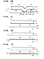
- Figs. 1A to 1E are views that explain an exemplary arrangement of a detection apparatus 100 according to the first embodiment
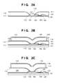
- Figs. 2A to 2C are views that explain an exemplary method of manufacturing the detection apparatus 100 according to the first embodiment
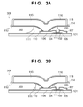
- Figs. 3A and 3B are views that explain a modification of the detection apparatus 100 according to the first embodiment
- Fig. 4 is a view that explains a modification of the detection apparatus 100 according to the first embodiment
- Fig. 5 is a view that explains a modification of the detection apparatus 100 according to the first embodiment
- Fig. 6 is a view that explains an example of the arrangement of a detection apparatus 600 according to the second embodiment
- Figs. 7A to 7C are views that explain an exemplary arrangement of a detection apparatus 700 according to the third embodiment
- Figs. 8A and 8B are views that explain an exemplary arrangement of a detection apparatus 800 according to the fourth embodiment
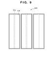
- Fig. 9 is a view that explains an exemplary arrangement of a detection apparatus 900 according to the fifth embodiment.
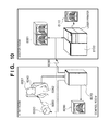
- Fig. 10 is a view that explains an exemplary detection system using the detection apparatus according to each embodiment.
- Fig. 1A is a plan view of the detection apparatus 100 including a plurality of pixels, with attention being paid to one pixel.
- Fig. 1B is a schematic sectional view of the pixel taken along a line A - A.
- Fig. 1C is a schematic sectional view taken along a line B - B.
- Fig. 1D is a schematic sectional view of the pixel taken along a line C - C.
- Fig. 1E is a schematic sectional view taken along a line D - D.
- Fig. 1A shows only partial components.
- the detection apparatus 100 includes transistors 109 as switching elements and photoelectric conversion elements 117 as conversion elements. Each transistor 109 formed over a substrate 101 is arranged between the corresponding photoelectric conversion element 117 and the substrate 101.
- the transistor 109 includes a gate electrode (control electrode) 102, a gate insulating film 104, a first semiconductor layer 105, a source electrode (one of the main electrodes) 106, and a drain electrode (the other of the main electrodes) 107.
- the photoelectric conversion element 117 includes a lower electrode (one electrode) 114, a PIN-type second semiconductor layer 115, and an upper electrode (the other electrode) 116.
- the lower electrode 114 is electrically connected to the source electrode 106.
- the gate electrode 102 is electrically connected to a gate line (control line) 103.
- the drain electrode 107 is electrically connected to a signal line 108.
- the upper electrode 116 is also electrically connected to a bias line (not shown).
- incident light is converted into charge.
- a voltage is applied to the gate electrode 102 via the gate line 103, an electrical signal corresponding to the charge is output to the signal line 108 via the transistor 109.
- the transistor 109, the gate line 103, and the signal line 108 are located at positions where they overlap the photoelectric conversion element 117. That is, the photoelectric conversion element 117 is located over the substrate 101 and is arranged over the gate line 103, the signal line 108, and the transistor 109.
- a first protective film 110 covers the transistor 109 except for a portion connected to the lower electrode 114.
- the upper surface of a second protective film 112 is in contact with the lower surface of the photoelectric conversion element 117 except for a portion connected to the transistor 109.
- a third protective film 118 covers the upper and side surfaces of the photoelectric conversion element 117.
- the first and second protective films 110 and 112 are in contact with each other around the connected portion between the lower electrode 114 and the source electrode 106.
- the second and third protective films 112 and 118 are in contact with each other around the side surfaces of the photoelectric conversion element 117. That is, the first, second, and third protective films 110, 112, and 118 enclose the transistor 109 and the photoelectric conversion element 117.
- a space 120 is formed between the first protective film 110 and the second protective film 112.
- the space 120 is generally formed by an air layer, but may be mixed with a gas generated in the process of manufacturing the detection apparatus 100 or may be a vacuum.
- the space 120 exists in at least part of the intervals between the lower electrode 114 and the gate line 103 and between the lower electrode 114 and the signal line 108.
- the space 120 exists in at least part of the intervals between the lower electrode 114 and the gate electrode 102 and between the lower electrode 114 and the drain electrode 107. That is, the lower electrode 114 is arranged over the transistor 109 and the signal line 108 through the space 120 between the lower electrode 114 and the drain electrode 107 or the signal line 108.
- the lower electrode 114 is arranged over the transistor 109 and the gate line 103 through the space 120 between the lower electrode 114 and the gate electrode 102 or the gate line 103. This makes it possible to reduce parasitic capacitances between the lower electrode 114 and the electrodes of the transistor 109 (the gate and drain electrodes in Figs. 1A to 1E ) and between the lower electrode 114 and the conductive lines (the gate and signal lines in Figs. 1A to 1E ).
- FIG. 2A to 2C An example of a method of manufacturing the detection apparatus 100 according to this embodiment will be described next with reference to Figs. 2A to 2C .
- Figs. 2A to 2C explain the manufacturing steps with reference to the schematic sectional view taken along the line A - A in Fig. 1A , other pixels are manufactured in the same steps.
- a metallic thin film is deposited on the substrate 101 and patterned by the photolithography method or the like to form the gate electrode 102 and the gate line 103.
- the substrate 101 is formed from, for example, glass, and the metallic thin film is formed from, for example, Al.
- the gate insulating film 104 is formed on the gate electrode 102 by the plasma CVD method or the like.
- the gate insulating film 104 is formed from, for example, silicon nitride.
- the first semiconductor layer 105 is formed to cover the gate electrode 102 by the plasma CVD method or the like.
- the first semiconductor layer 105 is formed from, for example, amorphous silicon.
- a metallic thin film is then deposited on the first semiconductor layer 105 and patterned by the photolithography method or the like to form the source electrode 106, the drain electrode 107, and the signal line 108. With the above process, the transistor 109 is formed.
- the first protective film 110 is deposited on the source electrode 106, the drain electrode 107, and the signal line 108 by the plasma CVD method or the like.
- the first protective film 110 is formed from, for example, silicon nitride.
- the thickness of the first protective film 110 can be, for example, 300 nm or more.
- An interlayer insulating film 111 is formed on the first protective film 110 by coating such as spray coating or spin coating. With this process, the interlayer insulating film 111 is formed to cover the gate line 103, the signal line 108, and the transistor 109.
- the interlayer insulating film 111 is formed from an organic resin such as acrylic resin which has a heatproof temperature of 200°C or more.
- the thickness of the interlayer insulating film 111 can be, for example, 300 nm or more.
- the thickness of the interlayer insulating film 111 may be, for example, 10 ⁇ m or less or 6 ⁇ m or less.
- the interlayer insulating film 111 is patterned to expose part of the first protective film 110 on the source electrode 106. Since the first protective film 110 and the interlayer insulating film 111 are formed from different materials, it is possible to remove only the interlayer insulating film 111 on the first protective film 110 without removing the first protective film 110.
- the second protective film 112 is then deposited on the resultant structure.
- the second protective film 112 is formed from, for example, silicon nitride.
- the thickness of the second protective film 112 can be, for example, 100 nm or more.
- the first protective film 110 comes into contact with the second protective film 112 over the source electrode 106.
- part of the source electrode 106 is exposed by continuously patterning part of an area 121 where the first protective film 110 is in contact with the second protective film 112.
- the first protective film 110 and the second protective film 112 are formed from the same material, it is possible to continuously pattern these protective films. This patterning is performed to leave an outer circumferential portion of the area 121 where the first protective film 110 is in contact with the second protective film 112. This leaves part of the area 121, where the first protective film 110 is in contact with the second protective film 112, around the contact hole 113. That is, the interlayer insulating film 111 is packaged around the contact hole 113.
- a metallic thin film is deposited on the second protective film 112 and the contact hole 113 by the sputtering method or the like and patterned by the photolithography method or the like to form the lower electrode 114.
- This patterning forms the lower electrode 114 partitioned for each pixel of the detection apparatus 100.
- part of the second protective film 112 is exposed between the lower electrode 114 of one pixel and the lower electrode of an adjacent pixel.
- the PIN-type second semiconductor layer 115 is formed by the plasma CVD method or the like so as to fit inside the lower electrode 114.
- the second semiconductor layer 115 may protrude from the lower electrode 114.
- a metallic thin film is deposited on the second semiconductor layer 115 by the sputtering method or the like and patterned so as to fit inside the second semiconductor layer 115, thereby forming the upper electrode 116.
- the photoelectric conversion element 117 is formed.
- the third protective film 118 is deposited on the photoelectric conversion element 117 by the sputtering method or the like.
- the third protective film 118 is formed from, for example, silicon nitride.
- the thickness of the third protective film 118 can be, for example, 500 nm or more.
- the second protective film 112 is in contact with the third protective film 118 between adjacent pixels. That is, in this structure, the interlayer insulating film 111 is packaged around them.
- the interlayer insulating film 111 is exposed by continuously patterning part of an area 122 where the second protective film 112 is in contact with the third protective film 118. Since the second protective film 112 and the third protective film 118 are formed from the same material, it is possible to continuously pattern these protective films. This patterning is performed to leave an outer circumferential portion of the area 122 where the second protective film 112 is in contact with the third protective film 118. This leaves part of the area 122, where the second protective film 112 is in contact with the third protective film 118, around the side surfaces of the photoelectric conversion element 117.
- the interlayer insulating film 111 is removed by performing isotropic etching such as dry etching on the exposed interlayer insulating film 111, thereby forming the space 120.
- the detection apparatus 100 according to this embodiment is manufactured.
- the dry etching on the interlayer insulating film 111 uses, for example, O 2 .
- Dry etching on each protective film uses, for example, a fluorine-based gas such as CF 4 + O 2 .
- An etching gas is selected in accordance with the etching rate necessary for the formation of each film and the necessary shape of each film after etching.
- the parasitic capacitance generated between the photoelectric conversion element 117 and the transistor 109 is reduced.
- the parasitic capacitance generated between the photoelectric conversion element 117, the gate line, and the signal line is reduced.
- the detection apparatus 100 may have the following arrangements.
- a detection apparatus 300 shown in Figs. 3A and 3B and a detection apparatus 400 shown in Fig. 4 will be described as modifications.
- the same reference numerals denote the same parts as in the detection apparatus 100 described with reference to Figs. 1A to 1E , and a description of them will be omitted.
- the detection apparatus 300 shown in Figs. 3A and 3B does not completely remove the interlayer insulating film 111 but leaves part of it.
- etching ends when the space 120 is formed in at least part of the intervals between the lower electrode 114 and the gate line 103 and between the lower electrode 114 and the signal line 108. This makes it possible to reduce the parasitic capacitance with the gate line 103 and the signal line 108 and make the interlayer insulating film 111 left without being removed support the photoelectric conversion element 117.
- Fig. 3A etching ends when the space 120 is formed in at least part of the intervals between the lower electrode 114 and the gate line 103 and between the lower electrode 114 and the signal line 108. This makes it possible to reduce the parasitic capacitance with the gate line 103 and the signal line 108 and make the interlayer insulating film 111 left without being removed support the photoelectric conversion element 117.
- the detection apparatus 400 does not use the second protective film 112. That is, the lower electrode 114 is in contact with the space 120. This can simplify the manufacturing process.
- the lower electrode 114 may be formed from a material with environmental stability.
- the lower electrode 114 is formed from indium tin oxide (ITO).
- ITO indium tin oxide
- the detection apparatus 400 can also be configured to leave part of the interlayer insulating film 111 described with reference to Fig. 3A or 3B .
- each embodiment may stack a scintillator layer on the photoelectric conversion element 117 of each pixel.
- a scintillator layer For a Tl-doped CsI columnar crystal 501 is deposited on the photoelectric conversion element 117.
- a fourth protective film 502 covers the columnar crystal 501.
- the present invention is not limited to this. It is possible to use any kind of film, for example, a conductive film, as long as it can be selectively removed after the formation of the photoelectric conversion element 117.
- a conductive film in a structure in which it is packaged by the first and second protective films 110 and 112 around the contact hole 113.
- an interlayer insulating film using an organic resin may be selected.
- This embodiment exemplifies a case in which the present invention is applied to a photoelectric conversion element using a MIS-type photoelectric conversion element.
- An example of the arrangement of a detection apparatus 600 according to this embodiment will be described with reference to Fig. 6.
- Fig. 6 corresponds to Fig. 1B described in the first embodiment.
- the same reference numerals denote the same parts, and a description of them will be omitted.
- a MIS-type photoelectric conversion element 604 includes a lower electrode 601, an insulating layer 602, and a second semiconductor layer 603.
- the lower electrode 601 is connected to a source electrode 106.
- An electrical signal converted by the MIS-type photoelectric conversion element 604 is output to a signal line 108 via a transistor 109.
- the insulating layer 602 is in contact with a third protective film 118 around the side surfaces of the second semiconductor layer 603.
- a space 120 exists in at least part of the intervals between the lower electrode 601 and a gate line 103 and between the lower electrode 601 and the signal line 108.
- the space 120 exists in at least part of the intervals between the lower electrode 601 and a gate electrode 102 and between the lower electrode 601 and a drain electrode 107. This makes it possible to reduce the parasitic capacitances between the lower electrode 601 and the electrodes of the transistor 109 and between the lower electrode 601 and the conductive lines.
- each modification described in the first embodiment may be applied to the detection apparatus 600 described in the second embodiment.
- a detection apparatus 700 which includes a plurality of pixels each including a MIS-type photoelectric conversion element as a photoelectric conversion element and a transistor as a switching element will be described with reference to Figs. 7A to 7C .
- Each pixel in Figs. 7A to 7C corresponds to the pixel in Fig. 6 described in the second embodiment.
- the same reference numerals denote the same parts, and a description of them will be omitted.
- the arrangement of a gate line 103 and a signal line 108 is the same as that shown in Fig. 1A .
- Fig. 7A is a plan view of this embodiment.
- Fig. 7B is a sectional view taken along a line E - E in Fig. 7A .
- Fig. 7C is a sectional view taken along a line F - F in Fig. 7A.
- Fig. 7A shows a 3 x 3 pixel group as an example of a plurality of pixels. Note that, in practice, many pixels, for example, 2000 x 2000 pixels, are arranged.
- the photoelectric conversion element of each pixel is partially coupled to other pixels, and insulating layers 602 and semiconductor layers 603 partly extend across a plurality of pixels.
- a third protective film 118 covers all the plurality of pixels.
- a space 120 exists in at least part of the intervals between a lower electrode 601 and the gate line 103 and between the lower electrode 601 and the signal line 108.
- the space 120 exists in at least part of the intervals between the lower electrode 601 and a gate electrode 102 and between the lower electrode 601 and a drain electrode 107. This makes it possible to reduce the parasitic capacitances between the lower electrode 601 and the electrodes of a transistor 109 and between the lower electrode 601 and the conductive lines.
- each modification described in the first embodiment may be applied to the detection apparatus 700 described in this embodiment.
- This embodiment is a modification of the detection apparatus according to the third embodiment.
- An example of the arrangement of a detection apparatus 800 according to this embodiment which includes a plurality of pixels each including a MIS-type photoelectric conversion element as a photoelectric conversion element and a transistor as a switching element will be described below with reference to Figs. 8A and 8B.
- Fig. 8A is a sectional view taken along a line E - E in Fig. 7A .
- Fig. 8B is a sectional view taken along a line G - G in Fig. 7A .
- a signal line 108 is arranged in a space 120 between a photoelectric conversion element and a transistor 109, and has a support portion connected to a conductive portion 801 partly extending from the transistor 109.
- the space 120 exists in at least part of each of the intervals between a lower electrode 601, a gate line 103, and the signal line 108.
- the space 120 also exists in at least part of the intervals between the lower electrode 601 and a gate electrode 102 and between the lower electrode 601 and a drain electrode 107. This makes it possible to reduce the parasitic capacitances between the lower electrode 601 and the electrodes of the transistor 109 and between the lower electrode 601 and the conductive lines. This can reduce the parasitic capacitance with the conductive lines, that is, the gate line 103 and the signal line 108.
- a process of connecting a transistor to a photoelectric conversion element in a method of manufacturing the detection apparatus 800, which is different from the above manufacturing process.
- a first protective film 110 is formed, and a first interlayer insulating film (not shown) is formed.
- a contact opening is formed in the first protective film 110 and the first interlayer insulating film.
- a conductive portion to connect the signal line 108, the lower electrode of the photoelectric conversion element, and the transistor 109 is formed.
- the second interlayer insulating film (not shown) is formed on the first interlayer insulating film and the conductive portion.
- a contact opening is formed in the second interlayer insulating film. As shown in Figs. 8A and 8B , this process forms two-level contact portions to connect the transistor to the photoelectric conversion element.
- a third protective film 118 covering the photoelectric conversion element improves the reliability.
- Placing a second protective film 112 on the transistor 109 side of the lower electrode 601 can further improve the reliability.
- a photoelectric conversion element a MIS- or PIN-type photoelectric conversion element can be used.
- Each modification described in the first embodiment may be applied to the detection apparatus 800 described in the fourth embodiment.
- This embodiment is a detection apparatus configured to make each photoelectric conversion element extends in the placing direction of a bias line to further improve the mechanical strength and reduce the resistance of the bias line.
- Fig. 9 is a plan view of a detection apparatus 900 including a 3 x 3 pixel group as an example, in which each photoelectric conversion element extends in the placing direction of a bias line 701.
- a semiconductor layer and an upper electrode 116 extend in the placing direction of the bias line 701.
- a third protective film 118 extends in a similar manner.
- This structure can improve the mechanical strength by coupling the respective pixels and reduce the resistance of each bias line. Reducing the resistance of each bias line can increase the driving speed of the detection apparatus, thereby improving image quality.
- Each modification described in the first embodiment may be applied to the detection apparatus 900 described in the fifth embodiment.
- Fig. 10 is a view showing an example of the application of the detection apparatus for radiation according to the present invention to an X-ray diagnostic system (radiation detection system).
- An X-ray 6060 as radiation generated by an X-ray tube 6050 (radiation source) is transmitted through a chest portion 6062 of an object to be examined or a patient 6061, and strikes a detection apparatus 6040 obtained by placing a scintillator including the columnar crystal 501 on the detection apparatus of the present invention.
- a detection conversion apparatus having a scintillator arranged on it forms a detection apparatus for radiation.
- This incident X-ray includes information inside the body of the patient 6061.
- the scintillator emits light in response to the incidence of X-rays, and photoelectrically converts the light, thereby obtaining electrical information. This information is converted into a digital signal.
- An image processor 6070 as a signal processing unit performs image processing of the information.
- the operator can observe the information on a display 6080 as a display unit in a control room.
- the radiation detection system includes at least a detection apparatus and a signal processing unit to process a signal from the detection apparatus.
- a transmission processing unit such as a telephone line 6090 or the like.
- a display 6081 serving as a display unit in a doctor room in a different place can display the information.
- a recording unit such as an optical disk can store the information. This allows a doctor in a remote place to perform diagnosis.
- a film processor 6100 as a recording unit can record the information on a film 6110 as a recording medium.
- a detection apparatus for radiation may use conversion elements which directly convert radiation into charge.
- Each conversion element to directly convert radiation into charge can be formed by using the second semiconductor layer to convert incident radiation into charge in place of the second semiconductor layer 115 or the second semiconductor layer 603 which converts incident light into charge.
- a detection apparatus comprising a substrate (101); a switching element (109) arranged over the substrate and including a plurality of electrodes (102, 106, 107); a conductive line (103, 108) arranged over the substrate and electrically connected to a first electrode (102, 107) of the plurality of electrodes of the switching element; and a conversion element (117) including a semiconductor layer (115, 603) arranged over the switching element and the conductive line and arranged between two electrodes (114, 116), one electrode (114) of the two electrodes being electrically connected to a second electrode (106) of the plurality of electrodes of the switching element, is provided.
- the one electrode of the conversion element is arranged over the switching element and the conductive line through a space (120) formed between the one electrode and the
Landscapes
- Solid State Image Pick-Up Elements (AREA)
- Light Receiving Elements (AREA)
- Photometry And Measurement Of Optical Pulse Characteristics (AREA)
- Transforming Light Signals Into Electric Signals (AREA)
Applications Claiming Priority (2)
| Application Number | Priority Date | Filing Date | Title |
|---|---|---|---|
| JP2010092626 | 2010-04-13 | ||
| JP2011029087A JP2011238897A (ja) | 2010-04-13 | 2011-02-14 | 検出装置及びその製造方法並びに検出システム |
Publications (2)
| Publication Number | Publication Date |
|---|---|
| EP2378554A2 true EP2378554A2 (de) | 2011-10-19 |
| EP2378554A3 EP2378554A3 (de) | 2013-11-13 |
Family
ID=44343205
Family Applications (1)
| Application Number | Title | Priority Date | Filing Date |
|---|---|---|---|
| EP11158404.1A Withdrawn EP2378554A3 (de) | 2010-04-13 | 2011-03-16 | Erkennungsvorrichtung, Herstellungsverfahren dafür und Erkennungssystem |
Country Status (5)
| Country | Link |
|---|---|
| US (1) | US8785873B2 (de) |
| EP (1) | EP2378554A3 (de) |
| JP (1) | JP2011238897A (de) |
| CN (1) | CN102222675B (de) |
| RU (1) | RU2474922C2 (de) |
Families Citing this family (8)
| Publication number | Priority date | Publication date | Assignee | Title |
|---|---|---|---|---|
| JP2012209421A (ja) * | 2011-03-30 | 2012-10-25 | Sony Corp | 固体撮像装置及び電子機器 |
| JP5709810B2 (ja) | 2012-10-02 | 2015-04-30 | キヤノン株式会社 | 検出装置の製造方法、その検出装置及び検出システム |
| JP6099035B2 (ja) * | 2012-10-12 | 2017-03-22 | Nltテクノロジー株式会社 | 光電変換装置及びその製造方法並びにx線画像検出装置 |
| JP2014236162A (ja) * | 2013-06-04 | 2014-12-15 | キヤノン株式会社 | 検出装置、その製造方法及び放射線検出システム |
| JP6232589B2 (ja) * | 2013-06-24 | 2017-11-22 | パナソニックIpマネジメント株式会社 | 固体撮像装置およびその製造方法 |
| US10126437B1 (en) * | 2017-05-15 | 2018-11-13 | Prismatic Sensors Ab | Detector for x-ray imaging |
| CN109742126B (zh) * | 2019-01-11 | 2022-02-11 | 京东方科技集团股份有限公司 | 显示基板及其制备方法、显示面板、显示装置 |
| CN115101550B (zh) * | 2022-01-19 | 2025-08-26 | 友达光电股份有限公司 | 感测装置及其制造方法 |
Citations (1)
| Publication number | Priority date | Publication date | Assignee | Title |
|---|---|---|---|---|
| US20030226974A1 (en) | 2002-06-11 | 2003-12-11 | Canon Kabushiki Kaisha | Radiation detecting apparatus, manufacturing method therefor, and radiation image pickup system |
Family Cites Families (36)
| Publication number | Priority date | Publication date | Assignee | Title |
|---|---|---|---|---|
| JPH06101552B2 (ja) | 1987-06-26 | 1994-12-12 | キヤノン株式会社 | 光電変換装置 |
| JPH0682820B2 (ja) | 1987-06-26 | 1994-10-19 | キヤノン株式会社 | 光電変換装置 |
| US6069393A (en) | 1987-06-26 | 2000-05-30 | Canon Kabushiki Kaisha | Photoelectric converter |
| US5262649A (en) * | 1989-09-06 | 1993-11-16 | The Regents Of The University Of Michigan | Thin-film, flat panel, pixelated detector array for real-time digital imaging and dosimetry of ionizing radiation |
| US5680229A (en) | 1991-03-27 | 1997-10-21 | Canon Kabushiki Kaisha | Photoelectric conversion apparatus with band gap variation in the thickness direction |
| JPH0529318A (ja) * | 1991-07-23 | 1993-02-05 | Toshiba Corp | 多層配線構造を有する半導体装置の製造方法 |
| US6020590A (en) * | 1998-01-22 | 2000-02-01 | Ois Optical Imaging Systems, Inc. | Large area imager with UV blocking layer |
| US5994157A (en) * | 1998-01-22 | 1999-11-30 | Ois Optical Imaging Systems, Inc. | Method of making a large area imager with UV Blocking layer, and corresponding imager |
| JP4401488B2 (ja) | 1998-09-01 | 2010-01-20 | キヤノン株式会社 | 光電変換装置 |
| JP4298081B2 (ja) | 1999-09-01 | 2009-07-15 | キヤノン株式会社 | 半導体装置及びそれを備えた放射線撮像システム |
| JP4249360B2 (ja) | 1999-11-02 | 2009-04-02 | 日東電工株式会社 | 回路基板およびその製造方法 |
| US6847039B2 (en) * | 2001-03-28 | 2005-01-25 | Canon Kabushiki Kaisha | Photodetecting device, radiation detecting device, and radiation imaging system |
| US6555467B2 (en) * | 2001-09-28 | 2003-04-29 | Sharp Laboratories Of America, Inc. | Method of making air gaps copper interconnect |
| JP2004015000A (ja) * | 2002-06-11 | 2004-01-15 | Canon Inc | 放射線検出装置及び放射線撮像システム |
| JP4054612B2 (ja) | 2002-06-11 | 2008-02-27 | キヤノン株式会社 | 放射線撮像装置 |
| US7006598B2 (en) * | 2002-08-09 | 2006-02-28 | Canon Kabushiki Kaisha | Imaging method and apparatus with exposure control |
| JP4067055B2 (ja) | 2003-10-02 | 2008-03-26 | キヤノン株式会社 | 撮像装置及びその製造方法、放射線撮像装置、放射線撮像システム |
| DE102004020979A1 (de) * | 2004-04-22 | 2005-11-17 | GSI Gesellschaft für Schwerionenforschung mbH | Dosimeter zur Erfassung von Neutronenstrahlung |
| US7282719B2 (en) | 2004-09-30 | 2007-10-16 | Canon Kabushiki Kaisha | Image pickup apparatus and radiation image pickup apparatus |
| JP4908947B2 (ja) * | 2005-07-11 | 2012-04-04 | キヤノン株式会社 | 変換装置、放射線検出装置、及び放射線検出システム |
| CN100539171C (zh) | 2005-07-11 | 2009-09-09 | 佳能株式会社 | 转换设备、放射检测设备和放射检测系统 |
| JP5043380B2 (ja) * | 2005-07-25 | 2012-10-10 | キヤノン株式会社 | 放射線検出装置および放射線検出システム |
| JP5207583B2 (ja) * | 2005-07-25 | 2013-06-12 | キヤノン株式会社 | 放射線検出装置および放射線検出システム |
| JP4773768B2 (ja) | 2005-08-16 | 2011-09-14 | キヤノン株式会社 | 放射線撮像装置、その制御方法及び放射線撮像システム |
| JP4886245B2 (ja) * | 2005-08-26 | 2012-02-29 | 株式会社東芝 | 放射線検出器 |
| RU2351038C2 (ru) | 2005-08-31 | 2009-03-27 | Кэнон Кабусики Кайся | Устройство обнаружения излучения, устройство формирования изображения излучения и система формирования изображения излучения |
| JP2007201246A (ja) * | 2006-01-27 | 2007-08-09 | Canon Inc | 光電変換装置及び放射線撮像装置 |
| JP4498283B2 (ja) | 2006-01-30 | 2010-07-07 | キヤノン株式会社 | 撮像装置、放射線撮像装置及びこれらの製造方法 |
| JP5196739B2 (ja) | 2006-06-09 | 2013-05-15 | キヤノン株式会社 | 放射線撮像装置及び放射線撮像システム |
| JP2008244411A (ja) * | 2007-03-29 | 2008-10-09 | Fujifilm Corp | 画像検出装置およびその製造方法 |
| JP5406473B2 (ja) | 2007-07-19 | 2014-02-05 | キヤノン株式会社 | 放射線検出装置 |
| JP2009252835A (ja) * | 2008-04-02 | 2009-10-29 | Fujifilm Corp | 電磁波検出素子 |
| JP2010011158A (ja) * | 2008-06-27 | 2010-01-14 | Fujifilm Corp | 検出素子 |
| JP5489542B2 (ja) * | 2008-07-01 | 2014-05-14 | キヤノン株式会社 | 放射線検出装置及び放射線撮像システム |
| TWI415283B (zh) * | 2009-02-18 | 2013-11-11 | Au Optronics Corp | X射線感測器及其製作方法 |
| JP5400507B2 (ja) | 2009-07-13 | 2014-01-29 | キヤノン株式会社 | 撮像装置及び放射線撮像システム |
-
2011
- 2011-02-14 JP JP2011029087A patent/JP2011238897A/ja active Pending
- 2011-03-16 EP EP11158404.1A patent/EP2378554A3/de not_active Withdrawn
- 2011-03-17 US US13/049,975 patent/US8785873B2/en not_active Expired - Fee Related
- 2011-04-08 CN CN201110087328.8A patent/CN102222675B/zh not_active Expired - Fee Related
- 2011-04-12 RU RU2011114300/28A patent/RU2474922C2/ru not_active IP Right Cessation
Patent Citations (1)
| Publication number | Priority date | Publication date | Assignee | Title |
|---|---|---|---|---|
| US20030226974A1 (en) | 2002-06-11 | 2003-12-11 | Canon Kabushiki Kaisha | Radiation detecting apparatus, manufacturing method therefor, and radiation image pickup system |
Also Published As
| Publication number | Publication date |
|---|---|
| EP2378554A3 (de) | 2013-11-13 |
| CN102222675A (zh) | 2011-10-19 |
| RU2474922C2 (ru) | 2013-02-10 |
| US20110248176A1 (en) | 2011-10-13 |
| JP2011238897A (ja) | 2011-11-24 |
| CN102222675B (zh) | 2014-05-28 |
| US8785873B2 (en) | 2014-07-22 |
| RU2011114300A (ru) | 2012-10-20 |
Similar Documents
| Publication | Publication Date | Title |
|---|---|---|
| US8785873B2 (en) | Detection apparatus, method of manufacturing the same, and detection system | |
| US8067743B2 (en) | Imaging apparatus and radiation imaging apparatus | |
| EP1246250B1 (de) | Fotoempfangende Vorrichtung, Strahlungsdetektor, und Strahlungsabbildungssystem | |
| US7791080B2 (en) | Image TFT array of a direct X-ray image sensor and method of fabricating the same | |
| US20130264485A1 (en) | Method of manufacturing radiation detection apparatus, radiation detection apparatus, and radiation imaging system | |
| US7550731B2 (en) | Coversion apparatus and imaging system | |
| JP5739359B2 (ja) | 撮像装置およびその製造方法ならびに撮像表示システム | |
| JP2013235934A (ja) | 検出装置、検出システム、及び、検出装置の製造方法 | |
| JP2022504994A (ja) | 放射線検出器及びその製造方法、電子デバイス | |
| JP2013235935A (ja) | 検出装置の製造方法、その検出装置及び検出システム | |
| JP2013161810A (ja) | 撮像装置およびその製造方法ならびに撮像表示システム | |
| US20140353470A1 (en) | Detection apparatus, method of manufacturing the same, and radiation detection system | |
| JP4498283B2 (ja) | 撮像装置、放射線撮像装置及びこれらの製造方法 | |
| US7026625B2 (en) | Radiation detection apparatus and system | |
| CN102446931A (zh) | 检测装置和辐射检测系统 | |
| JP2004296654A (ja) | 放射線撮像装置 | |
| JP4054612B2 (ja) | 放射線撮像装置 | |
| JP2004015000A (ja) | 放射線検出装置及び放射線撮像システム | |
| JP4018461B2 (ja) | 放射線検出装置及びその製造方法並びに放射線撮像システム | |
| JP2004165561A (ja) | 光電変換装置 | |
| JP2002343952A (ja) | 半導体装置及び放射線検出装置 | |
| JP2007165737A (ja) | 固体撮像装置 | |
| JP2002334984A (ja) | 検出装置および放射線撮像システム | |
| JP2005136330A (ja) | 撮像装置及び放射線撮像システム | |
| JP2003309256A (ja) | 放射線検出装置及びその製造方法 |
Legal Events
| Date | Code | Title | Description |
|---|---|---|---|
| AK | Designated contracting states |
Kind code of ref document: A2 Designated state(s): AL AT BE BG CH CY CZ DE DK EE ES FI FR GB GR HR HU IE IS IT LI LT LU LV MC MK MT NL NO PL PT RO RS SE SI SK SM TR |
|
| AX | Request for extension of the european patent |
Extension state: BA ME |
|
| RIN1 | Information on inventor provided before grant (corrected) |
Inventor name: MOCHIZUKI, CHIORI Inventor name: FUJIYOSHI, KENTARO Inventor name: KAWANABE, JUN Inventor name: WATANABE, MINORU Inventor name: ISHII, TAKAMASA |
|
| PUAI | Public reference made under article 153(3) epc to a published international application that has entered the european phase |
Free format text: ORIGINAL CODE: 0009012 |
|
| PUAL | Search report despatched |
Free format text: ORIGINAL CODE: 0009013 |
|
| AK | Designated contracting states |
Kind code of ref document: A3 Designated state(s): AL AT BE BG CH CY CZ DE DK EE ES FI FR GB GR HR HU IE IS IT LI LT LU LV MC MK MT NL NO PL PT RO RS SE SI SK SM TR |
|
| AX | Request for extension of the european patent |
Extension state: BA ME |
|
| RIC1 | Information provided on ipc code assigned before grant |
Ipc: H01L 31/18 20060101ALI20131007BHEP Ipc: H01L 27/144 20060101AFI20131007BHEP Ipc: H01L 27/146 20060101ALI20131007BHEP |
|
| 17P | Request for examination filed |
Effective date: 20140318 |
|
| RBV | Designated contracting states (corrected) |
Designated state(s): AL AT BE BG CH CY CZ DE DK EE ES FI FR GB GR HR HU IE IS IT LI LT LU LV MC MK MT NL NO PL PT RO RS SE SI SK SM TR |
|
| GRAJ | Information related to disapproval of communication of intention to grant by the applicant or resumption of examination proceedings by the epo deleted |
Free format text: ORIGINAL CODE: EPIDOSDIGR1 |
|
| RIC1 | Information provided on ipc code assigned before grant |
Ipc: H01L 27/144 20060101AFI20140407BHEP Ipc: H01L 31/18 20060101ALI20140407BHEP Ipc: H01L 27/146 20060101ALI20140407BHEP |
|
| GRAP | Despatch of communication of intention to grant a patent |
Free format text: ORIGINAL CODE: EPIDOSNIGR1 |
|
| INTG | Intention to grant announced |
Effective date: 20140522 |
|
| STAA | Information on the status of an ep patent application or granted ep patent |
Free format text: STATUS: THE APPLICATION HAS BEEN WITHDRAWN |
|
| 18W | Application withdrawn |
Effective date: 20140908 |