EP2259301A2 - Verfahren zur Vorbereitung und zum Zusammenbau von Substraten - Google Patents
Verfahren zur Vorbereitung und zum Zusammenbau von Substraten Download PDFInfo
- Publication number
- EP2259301A2 EP2259301A2 EP10177601A EP10177601A EP2259301A2 EP 2259301 A2 EP2259301 A2 EP 2259301A2 EP 10177601 A EP10177601 A EP 10177601A EP 10177601 A EP10177601 A EP 10177601A EP 2259301 A2 EP2259301 A2 EP 2259301A2
- Authority
- EP
- European Patent Office
- Prior art keywords
- wafer
- stage
- routing
- assembling
- wafers
- Prior art date
- Legal status (The legal status is an assumption and is not a legal conclusion. Google has not performed a legal analysis and makes no representation as to the accuracy of the status listed.)
- Granted
Links
Images


Classifications
-
- H—ELECTRICITY
- H10—SEMICONDUCTOR DEVICES; ELECTRIC SOLID-STATE DEVICES NOT OTHERWISE PROVIDED FOR
- H10P—GENERIC PROCESSES OR APPARATUS FOR THE MANUFACTURE OR TREATMENT OF DEVICES COVERED BY CLASS H10
- H10P95/00—Generic processes or apparatus for manufacture or treatments not covered by the other groups of this subclass
-
- H—ELECTRICITY
- H10—SEMICONDUCTOR DEVICES; ELECTRIC SOLID-STATE DEVICES NOT OTHERWISE PROVIDED FOR
- H10P—GENERIC PROCESSES OR APPARATUS FOR THE MANUFACTURE OR TREATMENT OF DEVICES COVERED BY CLASS H10
- H10P52/00—Grinding, lapping or polishing of wafers, substrates or parts of devices
-
- H—ELECTRICITY
- H10—SEMICONDUCTOR DEVICES; ELECTRIC SOLID-STATE DEVICES NOT OTHERWISE PROVIDED FOR
- H10P—GENERIC PROCESSES OR APPARATUS FOR THE MANUFACTURE OR TREATMENT OF DEVICES COVERED BY CLASS H10
- H10P90/00—Preparation of wafers not covered by a single main group of this subclass, e.g. wafer reinforcement
- H10P90/19—Preparing inhomogeneous wafers
- H10P90/1904—Preparing vertically inhomogeneous wafers
- H10P90/1906—Preparing SOI wafers
- H10P90/1914—Preparing SOI wafers using bonding
-
- H—ELECTRICITY
- H10—SEMICONDUCTOR DEVICES; ELECTRIC SOLID-STATE DEVICES NOT OTHERWISE PROVIDED FOR
- H10P—GENERIC PROCESSES OR APPARATUS FOR THE MANUFACTURE OR TREATMENT OF DEVICES COVERED BY CLASS H10
- H10P90/00—Preparation of wafers not covered by a single main group of this subclass, e.g. wafer reinforcement
- H10P90/19—Preparing inhomogeneous wafers
- H10P90/1904—Preparing vertically inhomogeneous wafers
- H10P90/1906—Preparing SOI wafers
- H10P90/1914—Preparing SOI wafers using bonding
- H10P90/1916—Preparing SOI wafers using bonding with separation or delamination along an ion implanted layer, e.g. Smart-cut
-
- H—ELECTRICITY
- H10—SEMICONDUCTOR DEVICES; ELECTRIC SOLID-STATE DEVICES NOT OTHERWISE PROVIDED FOR
- H10P—GENERIC PROCESSES OR APPARATUS FOR THE MANUFACTURE OR TREATMENT OF DEVICES COVERED BY CLASS H10
- H10P90/00—Preparation of wafers not covered by a single main group of this subclass, e.g. wafer reinforcement
- H10P90/19—Preparing inhomogeneous wafers
- H10P90/1904—Preparing vertically inhomogeneous wafers
- H10P90/1906—Preparing SOI wafers
- H10P90/1922—Preparing SOI wafers using silicon etch back techniques, e.g. BESOI or ELTRAN
-
- H—ELECTRICITY
- H10—SEMICONDUCTOR DEVICES; ELECTRIC SOLID-STATE DEVICES NOT OTHERWISE PROVIDED FOR
- H10W—GENERIC PACKAGES, INTERCONNECTIONS, CONNECTORS OR OTHER CONSTRUCTIONAL DETAILS OF DEVICES COVERED BY CLASS H10
- H10W10/00—Isolation regions in semiconductor bodies between components of integrated devices
- H10W10/10—Isolation regions comprising dielectric materials
- H10W10/181—Semiconductor-on-insulator [SOI] isolation regions, e.g. buried oxide regions of SOI wafers
Definitions
- the invention relates to the field of assembling wafers or slices or layers of material, notably semiconductors, and of their preparation with the purpose of assembling them.
- molecular adhesion allows to assemble flat structures of low surface roughness.
- wafers of material used in microelectronics such as, for example, wafers in silicon, or III-V material (AsGa, InP) or glass or fused silica or vitreous fused silica glass substrates.
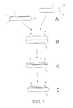
- the known methods for manufacturing SOI material which use molecular adhesion, implement two wafers 2, 4 of silicon ( figure 1 , part A), of which at least one of the two has a layer 6 of oxide on the surface.
- FIG. 2 represents, in greater detail, an example of a chamfer zone 5, of width L (measured on a plane parallel to the mean plane P of the wafer) of a wafer 4, of thickness e.
- the assembling firstly comprises a surface preparation stage, a putting together stage ( figure 1 , part B), generally followed by a heat treatment stage.
- this heat treatment is performed at 1100°C for 2 hours for SOI substrates.
- part C at least one of the two wafers is thinned out via surface edge grinding and/or mechanical polishing and/or mechano-chemical polishing.
- the chamfers 5 and 7 generate the existence of a non-bonded zone on the wafer edges.
- a membrane 8 made in silicon remains bonded to the centre, but detached on the edges, as visible in figure 1 , part C.
- the detached edge of the membrane must be removed, as it is likely to break in an uncontrolled manner and introduce particles on the other surfaces, and notably on surface 9 of the membrane 8, or on components made in the membrane 8.
- This routing is normally performed via mechanical means.
- This phenomenon is also important in the case where at least one of the two wafers contains all or part of an electronic or opto-electronic device, or a micro-system, or a nano-system or another component.
- Another problem is the marking of one or both of the two wafers 2 and 4, generally on the support wafer, with the purpose of providing specific information such as for example identification information of a batch.
- a marking generally via etching, induces a greater number of particles than on bulk wafers.
- the invention firstly relates to a method for assembling a first and a second wafer of material, comprising:
- a machining, or routing or eliminating or trimming stage of the matter in a peripheral section of at least the first wafer is thus performed before bonding or assembling the two wafers together.
- a thinning out stage of at least the first wafer can then be carried out, leaving a layer on the second wafer. A transplanting or transferring of this layer is thus achieved.
- the invention also relates to a method for transplanting or transferring a layer of material, circuits or components, known as transplant or transfer layer, comprising:
- This transplanting or transferring is performed via assembling the first and second wafers and then thinning out the first wafer.
- the first wafer of the method for assembling, transplanting or transferring is for example a chamfered wafer, bearing at least one chamfered edge.
- the routing or trimming thus relates to at least a part of the chamfered edge. It can also eat into a part, normally peripheral, of the transplant or transfer layer.
- the method for assembling or transplanting according to the invention thus allows to obtain a structure with a first wafer, possibly chamfered, perfectly routed before assembling, the routing or trimming being devoid of the problems developed above in the context of the prior art, problems due to the existence of a second wafer.
- Routing or trimming stages before assembling can be performed before or after possible surface preparation stages with the purpose of assembling or transplanting.
- the first wafer can be routed or trimmed through its entire thickness, or through its lesser thickness, for example equal to or greater than the final thickness of the layer that is sought after or transplanted onto the second wafer.
- the routing or trimming can also be performed over a thickness that is less than this final thickness.
- the thickness of the routing or trimming can be such that the routed wafer has, after routing or trimming, a dimension or diameter less than the other wafer.
- the width measured on the plane of the wafer, on which the upper wafer is routed or trimmed, is greater than or equal to the width of the rollover or chamfer.
- It can also have a width greater than or equal to the width of the zone which can not be bonded or assembled due to the rollover or chamfer.
- the first wafer can have a zone or a weakened or cleavage or fracture plane, created in depth for example by hydrogen implantation or by the creation of a buried porous zone or by the creation of a removable bonding interface.
- this routed wafer can be recycled, without the need of routing before bonding onto a new substrate.
- a new weakened a cleavage or fracture plane can thus be created, then it can be directly assembled with a new substrate.
- the assembling of the two wafers can be performed via molecular adhesion or via bonding, through the adding of matter such as for example adhesive or wax.
- the routing or trimming stage can be performed in a regular manner around the first wafer.
- the routing or trimming stage can also be performed in an irregular manner, creating at least one marking zone in at least one of the wafers. A marking stage in at least one of these marking zones can then be carried out.
- the object of the invention is also a method for assembling a first and a second wafer of material, comprising:
- One of the wafers for example the first, can have at least one chamfered edge.
- the invention thus allows to make a specific zone, for example with the purpose of marking a wafer, whether the routing or trimming takes place before or after the assembling of the wafers.
- a thinning out stage of one of the two wafers can take place before or after routing or trimming , leaving at least one layer on the other wafer.
- the process can comprise one or several of the following characteristics or stages:
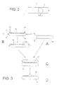
- Figure 3 parts A-D, represents stages of a method according to the invention.
- Two wafers 12 and 14 are chosen, for example two wafers of semiconductor material, such as standard silicon wafers.
- These wafers can typically have a thickness of between 300 ⁇ m and 800 ⁇ m. They are for example wafers of 100 mm or 200 mm or 300 mm in diameter.
- edges 15 and 17 are chamfered.
- Components or circuits 16 may have previously been made in the wafer 12, but the invention also relates to the case of a wafer 12 absent of any circuit, the reference 16 thus designating a layer of material to be transplanted or transferred onto the wafer 14.
- the surface of this layer 16 of circuits or material to be transplanted or transferred lies flush with the surface of the wafer 12.
- a routing or matter eliminating or trimming stage is then performed ( figure 3 , part B), starting from the face 19 of the wafer 12 (thus following a direction indicated by the arrows 13) to be assembled with the wafer 14, over a thickness ed and a width Ld. It is also possible to perform a routing or trimming in the direction indicated by the arrows 11, that meaning substantially parallel to the principal plane of the wafer 12. A routing or trimming in the two combined directions is also possible.
- the width Ld is measured on a plane parallel to the mean plane of the wafer.
- Ld is preferably greater than or equal to the width L of the rollover edge or the chamfer ( figure 2 ). It can be from about a few hundred ⁇ m to a few mm, for example of between 100 ⁇ m and 5 mm.
- Ld is notably greater than L in the case where the non-bonding zone or zone which can not adhere to a substrate after assembling, as illustrated in stage C of figure 1 , is itself greater than L.
- this "non-bonding" or “non-assembling" zone depends on the manner the rollover edge is made on the wafer 12 but also on the wafer 14.
- width L can also depend on the technical stages that could have been previously performed on the upper wafer 12 and on the support wafer 14.
- some stages can increase the width of this non-bonded zone (for example oxidising or depositing stages), others can reduce this said width (for example a levelling or flattening or polishing stage).
- Ld can therefore be greater than or equal to the width of this non-bonding or non-assembling zone.
- the thickness ed will be less than the thickness e of the wafer. It can be substantially equal to or greater or lesser than the thickness of the layer 16 (stage D, figure 3 ) or of the membrane to be obtained after the future thinning out or transplanting stage onto the wafer 14.
- ed can be about a few ⁇ m or between 1 ⁇ m (or 10 ⁇ m) and 100 ⁇ m or even between 5 ⁇ m and 60 ⁇ m.
- the layer 16 it can have a thickness, for example, between 1 ⁇ m and 60 ⁇ m.
- the assembling stage can be followed by an additional routing or trimming of the remaining section of substrate 12, as will be explained below.
- the routing or trimming stage before assembling can be performed in a mechanical and/or chemical (notably humid) and/or mechano-chemical manner and/or via plasma.
- the mechanic routing can be performed for example via "edge grinding” or "edge polishing".
- stage C it then proceeds with the assembling of the two wafers (stage C, figure 3 ) for example via molecular adhesion.
- the assembling comprises for example a surface preparation stage, a putting into contact stage and a heat treatment stage.
- This heat treatment stage is performed at a few hundred degrees Celsius, for example between 100 and 1200°C, or even 1100°C, and this for a time span from a few minutes to a few hours, for example between 10 minutes and 3 hours, or even 2 hours.
- stage D at least one of the two wafers is thinned down to the desired thickness, for example over a thickness greater than or equal to e-ed, via edge grinding and/or mechanical polishing and/or mechano-chemical polishing and/or chemical polishing.
- the thinned wafer is the previously routed wafer 13.
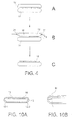
- Figure 4 part A, corresponds to the aforementioned case where the depth ed over which the wafer 12 was routed before assembling is insufficient to completely remove the layer 16 during the thinning out stage.
- Assembling which has led to the structure of figure 4 , part A, can thus be followed with an additional routing or trimming, from the edges 13 located on the side of the front face or from the assembling face, in order to obtain a routed zone over a thickness ed greater than that of the layer 16 ( figure 4 , part B).
- the assembling stage leads to the device represented in figure 5 , part B, which can then be thinned out as explained above.
- the wafer 12 then has a width or diameter less than that of the wafer 14.
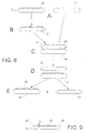
- the invention also applies to an initial substrate 22 in which a weakened or fracture plane 26 was made, for example via previous ion implantation (for example a hydrogen implantation) or via creating a buried porous zone, as explained for example in the document by S.S.Iyer and al. "Silicon wafer bonding technology for VLST and MEMS applications", published by INSPEC, 2002, Antony Rowe Ltd, or via creating a removable bonding interface.
- a weakened or fracture plane 26 was made, for example via previous ion implantation (for example a hydrogen implantation) or via creating a buried porous zone, as explained for example in the document by S.S.Iyer and al. "Silicon wafer bonding technology for VLST and MEMS applications", published by INSPEC, 2002, Antony Rowe Ltd, or via creating a removable bonding interface.
- a heat treatment allows to separate the substrate 22 on the ion implantation layer 26 of hydrogen ions ( figure 6 , part D).
- the invention such as is described above in connection with one of the figures 3-6 , also applies in the case where the initial substrate 12 and 22 has the shape illustrated in figure 9 , with a shoulder 25 on the edges of the wafer.
- These shoulders define a stiffening located at a depth P, for example lying between 50 nm and 2 ⁇ m.
- the routing stage allows to remove these shoulders.
- An ion implantation stage, for the creating of a weakened plane 26, can take place before or after this routing or trimming stage: a wafer is thus obtained which is identical to the one represented in part B of figure 6 .
- the following stages in figure 6 can thus be performed as described above.
- BSOI or thick SOI type structures can also be created in an efficient manner.
- the thinning out stage is then mechanic and/or mechano-chemical.
- electronic components are made in a wafer such as the wafer 12 ( figure 3A ) over a superficial thickness, for example, between 1 and 10 ⁇ m.
- This routing stage can be performed before surface preparation (for example via mechano-chemical levelling followed by chemical cleaning) and in order to reduce the number of cleansings before assembling.
- the routed wafer (comprising the components) is bonded via molecular adhesion onto the support wafer.
- the structure is then annealed for example at a temperature of 300°C and for a time span of between a few minutes and a few hours.
- the superficial wafer is then thinned out via surface edge grinding and mechano-chemical ( figure 3 , part D) and/or chemical polishing until a thickness de is obtained, for example, 10 ⁇ m.
- a transplanted layer, comprising the components, transferred onto a support wafer is thus obtained.
- the wafer 12 comprises components 16 and is covered on its surface with a protective layer 18, for example an oxide layer 18 ( figure 7 , part A). This can also be a bonding layer.
- a protective layer 18 for example an oxide layer 18 ( figure 7 , part A). This can also be a bonding layer.
- a crown 20 is defined via lithography which will correspond to the routing zone.
- a local chemical etching allows to eliminate, on this zone, the protective layer 18 ( figure 7 , part B).
- the edge of the substrate 12 is then etched ( figure 7 , part C), for example via chemical (ex. TMAH) or plasma etching.
- the wafer is then cleaned, for example via chemical cleaning.
- the cleaning is integrated into the chemical etching.
- a protective layer 18 initially coats the entire upper section of the wafer 12 as well as the edges 12-1 and 12-2, and possibly its lower section (in which case it coats the entire wafer).
- the routing operation will allow to eliminate the lateral zones of this wafer such as the hatched zone in figure 10B .
- a possible scaling or clearing due to the routing operation occurs at the point M of the coating layer 18 or in a zone of this layer near this point.
- a scaling occurring on the wafer can generate defects, some of which can show on the surface of the wafer.
- a point of the surface to be assembled, such as point N, remains intact despite routing.
- the protective layer 18 can be eliminated after routing and before assembling.
- Figures 8A-8D each represent a front view of a wafer 40 and 42 with a layer 41 and 43 of material around which routing was performed. This layer 41 and 43 is intended to be transplanted or transferred onto a second wafer, according to any one of the aforementioned embodiments.
- the wafer has a flat or a flattered zone 44.
- zones 50 and 51 represent zones or flats or flat surfaces which will allow to mark the support wafer.
- the zone 44 in figure 8A can also be used to mark the wafer.
- Such a zone allows to provide indications regarding the nature of the wafer or an identification number of a batch to which the wafer belongs.
- Irregular routing such as in figures 8A, 8C and 8D can also be performed when routing is performed after assembling, thus using the standard routing technique such as is illustrated in figures 1A-1D , and possibly with one or two processed wafers, thus comprising all or part of a component or circuit.
- the other processing stages can be those already described above.
- one of the wafers can have a chamfered edge, the routing can thus take place over a width at least equal to the width of the chamfered edge, measured on a plane parallel to that of the wafer.
- the assembling can take place via molecular adhesion or via bonding.
- the invention has the advantage of being able to be integrated into a method for manufacturing. This is notably the case when components are previously made in the wafers.
- the invention also applies in the case of non-chamfered wafers, a stage for routing or trimming or eliminating matter in a peripheral zone of one of these two wafers being nonetheless performed before assembling the two wafers.
- the other processing stages are similar to those described according to one or other of the embodiments described above or below.
- the method set forth in the invention is also well suited to the manufacturing of BSOI type material, or even to the transplanting of a layer of III-V material onto silicon for example.
- This wafer is then routed over a 1.5 mm wide zone which corresponds to the edge or the rollover edge of the wafer, as explained above.
- the surface of the wafer is then cleaned, for example via chemical and/or mechano-chemical cleaning stages.
- a surface edge grinding stage followed by a mechano-chemical polishing allows to thin the wafer down to the desired thickness in order to obtain the SOI substrate.
- This said method can apply to the transplanting of III-V material such as AsGa or InP onto another material such as a semiconductor notably silicon.
- This said method can also apply to the transplanting of semiconductor material such as Germanium or Germanium silicon (SiGe) onto a substrate made in another material such as a semiconductor, notably silicon.
- semiconductor material such as Germanium or Germanium silicon (SiGe)
- SiGe Germanium or Germanium silicon
- this method can be used to perform a transplanting of wafers of non-semiconductor material, for example wafers of insulating material such as glass or quartz, or piezoelectric material such as LiNbO3 or LiTaO3, which allows to obtain a perfectly routed thin film on a support of the same nature or of a different nature, for example a semiconductor substrate and notably silicon.
- non-semiconductor material for example wafers of insulating material such as glass or quartz, or piezoelectric material such as LiNbO3 or LiTaO3, which allows to obtain a perfectly routed thin film on a support of the same nature or of a different nature, for example a semiconductor substrate and notably silicon.
- the wafers of material prepared and assembled according to the invention are wafers of "bulk" material.
- the invention applies to wafers that can contain all or part of a component, for example an electronic, and/or an electro-optic, and/or an optic, and/or a magnetic component or a MEMS.
Landscapes
- Element Separation (AREA)
- Mechanical Treatment Of Semiconductor (AREA)
- Micromachines (AREA)
- Die Bonding (AREA)
Applications Claiming Priority (4)
| Application Number | Priority Date | Filing Date | Title |
|---|---|---|---|
| FR0350674A FR2860842B1 (fr) | 2003-10-14 | 2003-10-14 | Procede de preparation et d'assemblage de substrats |
| US56870004P | 2004-05-07 | 2004-05-07 | |
| PCT/EP2004/052548 WO2005038903A1 (en) | 2003-10-14 | 2004-10-14 | Method for preparing and assembling substrates |
| EP04791232.4A EP1676310B1 (de) | 2003-10-14 | 2004-10-14 | Verfahren zur herstellung und zusammenstellung von substraten |
Related Parent Applications (3)
| Application Number | Title | Priority Date | Filing Date |
|---|---|---|---|
| EP04791232.4A Division EP1676310B1 (de) | 2003-10-14 | 2004-10-14 | Verfahren zur herstellung und zusammenstellung von substraten |
| EP04791232.4A Division-Into EP1676310B1 (de) | 2003-10-14 | 2004-10-14 | Verfahren zur herstellung und zusammenstellung von substraten |
| EP04791232.4 Division | 2004-10-14 |
Publications (3)
| Publication Number | Publication Date |
|---|---|
| EP2259301A2 true EP2259301A2 (de) | 2010-12-08 |
| EP2259301A3 EP2259301A3 (de) | 2010-12-22 |
| EP2259301B1 EP2259301B1 (de) | 2020-08-19 |
Family
ID=34355518
Family Applications (3)
| Application Number | Title | Priority Date | Filing Date |
|---|---|---|---|
| EP04791232.4A Expired - Lifetime EP1676310B1 (de) | 2003-10-14 | 2004-10-14 | Verfahren zur herstellung und zusammenstellung von substraten |
| EP11173320.0A Expired - Lifetime EP2375443B1 (de) | 2003-10-14 | 2004-10-14 | Verfahren zum Herstellen und Zusammenbauen von Substraten |
| EP10177601.1A Expired - Lifetime EP2259301B1 (de) | 2003-10-14 | 2004-10-14 | Verfahren zur Vorbereitung und zum Zusammenbau von Substraten |
Family Applications Before (2)
| Application Number | Title | Priority Date | Filing Date |
|---|---|---|---|
| EP04791232.4A Expired - Lifetime EP1676310B1 (de) | 2003-10-14 | 2004-10-14 | Verfahren zur herstellung und zusammenstellung von substraten |
| EP11173320.0A Expired - Lifetime EP2375443B1 (de) | 2003-10-14 | 2004-10-14 | Verfahren zum Herstellen und Zusammenbauen von Substraten |
Country Status (7)
| Country | Link |
|---|---|
| US (1) | US20070072393A1 (de) |
| EP (3) | EP1676310B1 (de) |
| JP (1) | JP5032119B2 (de) |
| KR (1) | KR101148052B1 (de) |
| CN (2) | CN100555599C (de) |
| FR (1) | FR2860842B1 (de) |
| WO (1) | WO2005038903A1 (de) |
Cited By (2)
| Publication number | Priority date | Publication date | Assignee | Title |
|---|---|---|---|---|
| CN109786212A (zh) * | 2017-11-13 | 2019-05-21 | 台湾积体电路制造股份有限公司 | 晶片结构及其修整方法 |
| WO2024141481A1 (fr) * | 2022-12-28 | 2024-07-04 | Commissariat A L'energie Atomique Et Aux Energies Alternatives | Procédé de fabrication d'une structure multicouche comprenant une couche de silicium poreux |
Families Citing this family (61)
| Publication number | Priority date | Publication date | Assignee | Title |
|---|---|---|---|---|
| FR2871291B1 (fr) * | 2004-06-02 | 2006-12-08 | Tracit Technologies | Procede de transfert de plaques |
| FR2880184B1 (fr) | 2004-12-28 | 2007-03-30 | Commissariat Energie Atomique | Procede de detourage d'une structure obtenue par assemblage de deux plaques |
| JP4918229B2 (ja) * | 2005-05-31 | 2012-04-18 | 信越半導体株式会社 | 貼り合わせウエーハの製造方法 |
| FR2888400B1 (fr) | 2005-07-08 | 2007-10-19 | Soitec Silicon On Insulator | Procede de prelevement de couche |
| EP1911085B1 (de) * | 2005-07-08 | 2011-10-12 | S.O.I.Tec Silicon on Insulator Technologies | Verfahren zur herstellung eines films |
| JP4839818B2 (ja) * | 2005-12-16 | 2011-12-21 | 信越半導体株式会社 | 貼り合わせ基板の製造方法 |
| FR2899594A1 (fr) * | 2006-04-10 | 2007-10-12 | Commissariat Energie Atomique | Procede d'assemblage de substrats avec traitements thermiques a basses temperatures |
| US7846817B2 (en) * | 2007-03-26 | 2010-12-07 | Semiconductor Energy Laboratory Co., Ltd. | Method for manufacturing semiconductor device |
| EP1975998A3 (de) * | 2007-03-26 | 2013-12-04 | Semiconductor Energy Laboratory Co., Ltd. | Herstellungsverfahren einer Mehrzahl von SOI-Inselstrukturen |
| EP1993128A3 (de) | 2007-05-17 | 2010-03-24 | Semiconductor Energy Laboratory Co., Ltd. | Verfahren zur Herstellung eines SOI-Substrats |
| FR2917232B1 (fr) * | 2007-06-06 | 2009-10-09 | Soitec Silicon On Insulator | Procede de fabrication d'une structure pour epitaxie sans zone d'exclusion. |
| CN101743616B (zh) * | 2007-06-28 | 2012-02-22 | 株式会社半导体能源研究所 | 半导体装置的制造方法 |
| JP5507063B2 (ja) * | 2007-07-09 | 2014-05-28 | 株式会社半導体エネルギー研究所 | 半導体装置の作製方法 |
| DE102007025649B4 (de) * | 2007-07-21 | 2011-03-03 | X-Fab Semiconductor Foundries Ag | Verfahren zum Übertragen einer Epitaxie-Schicht von einer Spender- auf eine Systemscheibe der Mikrosystemtechnik |
| CN101620985B (zh) * | 2008-07-02 | 2011-05-11 | 联华电子股份有限公司 | 晶边蚀刻设备及其相关的晶片平坦化方法 |
| DE102008035055B3 (de) | 2008-07-26 | 2009-12-17 | X-Fab Semiconductor Foundries Ag | Verfahren zur Ausrichtung einer elektronischen CMOS-Struktur bezogen auf eine vergrabene Struktur bei gebondeten und rückgedünnten Stapeln von Halbleiterscheiben |
| FR2935536B1 (fr) * | 2008-09-02 | 2010-09-24 | Soitec Silicon On Insulator | Procede de detourage progressif |
| FR2935535B1 (fr) * | 2008-09-02 | 2010-12-10 | S O I Tec Silicon On Insulator Tech | Procede de detourage mixte. |
| EP2200077B1 (de) * | 2008-12-22 | 2012-12-05 | Soitec | Verfahren zur Bindung zweier Substrate |
| KR101550433B1 (ko) | 2009-01-30 | 2015-09-07 | 삼성전자주식회사 | 반도체 장치의 제조 방법 |
| US7927975B2 (en) | 2009-02-04 | 2011-04-19 | Micron Technology, Inc. | Semiconductor material manufacture |
| EP2246882B1 (de) * | 2009-04-29 | 2015-03-04 | Soitec | Verfahren zur Übertragung einer Schicht von einem Donatorsubstrat auf ein Handhabungssubstrat |
| CN101599451B (zh) * | 2009-07-10 | 2013-08-07 | 上海新傲科技股份有限公司 | 对带有绝缘埋层的半导体衬底进行边缘倒角的方法 |
| US8633090B2 (en) * | 2009-07-10 | 2014-01-21 | Shanghai Simgui Technology Co., Ltd. | Method for forming substrate with buried insulating layer |
| FR2950734B1 (fr) * | 2009-09-28 | 2011-12-09 | Soitec Silicon On Insulator | Procede de collage et de transfert d'une couche |
| FR2953988B1 (fr) * | 2009-12-11 | 2012-02-10 | S O I Tec Silicon On Insulator Tech | Procede de detourage d'un substrat chanfreine. |
| FR2957190B1 (fr) * | 2010-03-02 | 2012-04-27 | Soitec Silicon On Insulator | Procede de realisation d'une structure multicouche avec detourage par effets thermomecaniques. |
| FR2957189B1 (fr) * | 2010-03-02 | 2012-04-27 | Soitec Silicon On Insulator | Procede de realisation d'une structure multicouche avec detourage post meulage. |
| FR2961630B1 (fr) | 2010-06-22 | 2013-03-29 | Soitec Silicon On Insulator Technologies | Appareil de fabrication de dispositifs semi-conducteurs |
| US8338266B2 (en) | 2010-08-11 | 2012-12-25 | Soitec | Method for molecular adhesion bonding at low pressure |
| FR2964193A1 (fr) | 2010-08-24 | 2012-03-02 | Soitec Silicon On Insulator | Procede de mesure d'une energie d'adhesion, et substrats associes |
| US20120129318A1 (en) * | 2010-11-24 | 2012-05-24 | Semiconductor Energy Laboratory Co., Ltd. | Atmospheric pressure plasma etching apparatus and method for manufacturing soi substrate |
| FR2969373B1 (fr) * | 2010-12-20 | 2013-07-19 | St Microelectronics Crolles 2 | Procede d'assemblage de deux plaques et dispositif correspondant |
| JP2013008915A (ja) * | 2011-06-27 | 2013-01-10 | Toshiba Corp | 基板加工方法及び基板加工装置 |
| FR2980302A1 (fr) | 2011-09-20 | 2013-03-22 | St Microelectronics Crolles 2 | Procede de protection d'une couche d'un empilement vertical et dispositif correspondant |
| US8383460B1 (en) * | 2011-09-23 | 2013-02-26 | GlobalFoundries, Inc. | Method for fabricating through substrate vias in semiconductor substrate |
| JP5946260B2 (ja) * | 2011-11-08 | 2016-07-06 | 株式会社ディスコ | ウエーハの加工方法 |
| US9064770B2 (en) * | 2012-07-17 | 2015-06-23 | Taiwan Semiconductor Manufacturing Company, Ltd. | Methods for minimizing edge peeling in the manufacturing of BSI chips |
| US9481566B2 (en) | 2012-07-31 | 2016-11-01 | Soitec | Methods of forming semiconductor structures including MEMS devices and integrated circuits on opposing sides of substrates, and related structures and devices |
| JP6116155B2 (ja) * | 2012-08-20 | 2017-04-19 | 株式会社ディスコ | ウエーハの加工方法 |
| FR2995133A1 (fr) * | 2012-08-31 | 2014-03-07 | St Microelectronics Crolles 2 | Procede d'amincissement d'une tranche semiconductrice |
| TWI663025B (zh) * | 2012-09-24 | 2019-06-21 | 日商荏原製作所股份有限公司 | 研磨方法及研磨裝置 |
| CN104576350B (zh) * | 2013-10-23 | 2018-06-01 | 中芯国际集成电路制造(上海)有限公司 | 晶圆减薄方法 |
| CN105826161A (zh) * | 2015-01-07 | 2016-08-03 | 中芯国际集成电路制造(上海)有限公司 | 晶圆减薄方法 |
| FR3036223B1 (fr) | 2015-05-11 | 2018-05-25 | Commissariat A L'energie Atomique Et Aux Energies Alternatives | Procede de collage direct de substrats avec amincissement des bords d'au moins un des deux substrats |
| JP6380245B2 (ja) * | 2015-06-15 | 2018-08-29 | 信越半導体株式会社 | Soiウェーハの製造方法 |
| DE102015118042A1 (de) | 2015-10-22 | 2017-04-27 | Nexwafe Gmbh | Verfahren und Vorrichtung zum Herstellen einer Halbleiterschicht |
| US10867836B2 (en) * | 2016-05-02 | 2020-12-15 | Taiwan Semiconductor Manufacturing Co., Ltd. | Wafer stack and fabrication method thereof |
| KR20180090494A (ko) * | 2017-02-03 | 2018-08-13 | 삼성전자주식회사 | 기판 구조체 제조 방법 |
| US10504716B2 (en) * | 2018-03-15 | 2019-12-10 | Taiwan Semiconductor Manufacturing Company Ltd. | Method for manufacturing semiconductor device and manufacturing method of the same |
| CN109545672A (zh) * | 2018-11-21 | 2019-03-29 | 德淮半导体有限公司 | 晶圆键合方法以及键合晶圆 |
| US12076820B2 (en) * | 2018-12-21 | 2024-09-03 | Tokyo Electron Limited | Substrate processing apparatus and substrate processing method |
| CN109712875B (zh) * | 2018-12-29 | 2020-11-20 | 上海华力微电子有限公司 | 晶圆直接键合方法 |
| CN110060958B (zh) * | 2019-04-22 | 2020-05-19 | 长江存储科技有限责任公司 | 半导体结构及半导体工艺方法 |
| CN110060957B (zh) * | 2019-04-22 | 2020-07-31 | 长江存储科技有限责任公司 | 半导体结构及半导体工艺方法 |
| US11482506B2 (en) * | 2020-03-31 | 2022-10-25 | Taiwan Semiconductor Manufacturing Company Limited | Edge-trimming methods for wafer bonding and dicing |
| JP7650587B2 (ja) * | 2021-02-26 | 2025-03-25 | 株式会社ディスコ | ウェーハの加工方法 |
| FR3120985B1 (fr) * | 2021-03-19 | 2023-03-31 | Soitec Silicon On Insulator | Procédé de fabrication d’une hétérostructure |
| CN113725151B (zh) * | 2021-08-30 | 2024-03-15 | 上海华虹宏力半导体制造有限公司 | 互连结构的形成方法 |
| EP4291006A3 (de) * | 2022-05-16 | 2023-12-27 | Samsung Display Co., Ltd. | Anzeigevorrichtung, elektronische vorrichtung damit und verfahren zur herstellung der anzeigevorrichtung |
| FR3135819B1 (fr) | 2022-05-18 | 2024-04-26 | Commissariat Energie Atomique | Procédé de transfert d'une couche depuis un substrat source vers un substrat destination |
Family Cites Families (42)
| Publication number | Priority date | Publication date | Assignee | Title |
|---|---|---|---|---|
| US4522049A (en) * | 1983-03-14 | 1985-06-11 | Aluminum Company Of America | Aluminum alloy food can body and method for making same |
| JP2535957B2 (ja) * | 1987-09-29 | 1996-09-18 | ソニー株式会社 | 半導体基板 |
| JPH0636413B2 (ja) * | 1990-03-29 | 1994-05-11 | 信越半導体株式会社 | 半導体素子形成用基板の製造方法 |
| US5476566A (en) * | 1992-09-02 | 1995-12-19 | Motorola, Inc. | Method for thinning a semiconductor wafer |
| JPH0799295A (ja) * | 1993-06-07 | 1995-04-11 | Canon Inc | 半導体基体の作成方法及び半導体基体 |
| JP3293736B2 (ja) * | 1996-02-28 | 2002-06-17 | キヤノン株式会社 | 半導体基板の作製方法および貼り合わせ基体 |
| US5668045A (en) * | 1994-11-30 | 1997-09-16 | Sibond, L.L.C. | Process for stripping outer edge of BESOI wafers |
| US5937312A (en) * | 1995-03-23 | 1999-08-10 | Sibond L.L.C. | Single-etch stop process for the manufacture of silicon-on-insulator wafers |
| US5869386A (en) * | 1995-09-28 | 1999-02-09 | Nec Corporation | Method of fabricating a composite silicon-on-insulator substrate |
| JPH10335195A (ja) * | 1997-05-27 | 1998-12-18 | Mitsubishi Materials Shilicon Corp | 張り合わせ基板の製造方法 |
| FR2771852B1 (fr) * | 1997-12-02 | 1999-12-31 | Commissariat Energie Atomique | Procede de transfert selectif d'une microstructure, formee sur un substrat initial, vers un substrat final |
| US6306729B1 (en) * | 1997-12-26 | 2001-10-23 | Canon Kabushiki Kaisha | Semiconductor article and method of manufacturing the same |
| JP3932369B2 (ja) * | 1998-04-09 | 2007-06-20 | 信越半導体株式会社 | 剥離ウエーハを再利用する方法および再利用に供されるシリコンウエーハ |
| JPH11354761A (ja) * | 1998-06-09 | 1999-12-24 | Sumitomo Metal Ind Ltd | Soi基板及びその製造方法 |
| US6093623A (en) * | 1998-08-04 | 2000-07-25 | Micron Technology, Inc. | Methods for making silicon-on-insulator structures |
| JP3515917B2 (ja) * | 1998-12-01 | 2004-04-05 | シャープ株式会社 | 半導体装置の製造方法 |
| JP2000223683A (ja) * | 1999-02-02 | 2000-08-11 | Canon Inc | 複合部材及びその分離方法、貼り合わせ基板及びその分離方法、移設層の移設方法、並びにsoi基板の製造方法 |
| JP4365920B2 (ja) * | 1999-02-02 | 2009-11-18 | キヤノン株式会社 | 分離方法及び半導体基板の製造方法 |
| JP4313874B2 (ja) * | 1999-02-02 | 2009-08-12 | キヤノン株式会社 | 基板の製造方法 |
| JP3472197B2 (ja) * | 1999-06-08 | 2003-12-02 | キヤノン株式会社 | 半導体基材及び太陽電池の製造方法 |
| US6664169B1 (en) * | 1999-06-08 | 2003-12-16 | Canon Kabushiki Kaisha | Process for producing semiconductor member, process for producing solar cell, and anodizing apparatus |
| US20020187595A1 (en) * | 1999-08-04 | 2002-12-12 | Silicon Evolution, Inc. | Methods for silicon-on-insulator (SOI) manufacturing with improved control and site thickness variations and improved bonding interface quality |
| EP1189266B1 (de) * | 2000-03-29 | 2017-04-05 | Shin-Etsu Handotai Co., Ltd. | Methode zur herstellung einer siliziumhalbleiterscheibe und einer soi-scheibe soiwe soi-scheibe |
| JP4846915B2 (ja) * | 2000-03-29 | 2011-12-28 | 信越半導体株式会社 | 貼り合わせウェーハの製造方法 |
| JP3991300B2 (ja) * | 2000-04-28 | 2007-10-17 | 株式会社Sumco | 張り合わせ誘電体分離ウェーハの製造方法 |
| JP3768069B2 (ja) * | 2000-05-16 | 2006-04-19 | 信越半導体株式会社 | 半導体ウエーハの薄型化方法 |
| FR2809867B1 (fr) * | 2000-05-30 | 2003-10-24 | Commissariat Energie Atomique | Substrat fragilise et procede de fabrication d'un tel substrat |
| JP2002134374A (ja) * | 2000-10-25 | 2002-05-10 | Mitsubishi Electric Corp | 半導体ウェハ、その製造方法およびその製造装置 |
| JP4149263B2 (ja) * | 2001-01-18 | 2008-09-10 | エルジー エレクトロニクス インコーポレーテッド | プラズマディスプレイパネル及びその駆動方法 |
| CN100454552C (zh) * | 2001-07-17 | 2009-01-21 | 信越半导体株式会社 | 贴合晶片的制造方法及贴合晶片、以及贴合soi晶片 |
| JP2003078115A (ja) * | 2001-08-30 | 2003-03-14 | Shin Etsu Handotai Co Ltd | Soiウェーハのレーザーマーク印字方法、及び、soiウェーハ |
| CN1172376C (zh) * | 2001-12-29 | 2004-10-20 | 中国科学院上海微系统与信息技术研究所 | 一种类似绝缘层上硅结构的材料及制备方法 |
| FR2837981B1 (fr) * | 2002-03-28 | 2005-01-07 | Commissariat Energie Atomique | Procede de manipulation de couches semiconductrices pour leur amincissement |
| WO2003098695A1 (en) * | 2002-05-20 | 2003-11-27 | Sumitomo Mitsubishi Silicon Corporation | Laminated substrate, method of manufacturing the substrate, and wafer outer periphery pressing jigs used for the method |
| EP2164096B1 (de) * | 2002-07-17 | 2012-09-05 | Soitec | Verfahren zur Glättung der Kontur einer nützlichen, auf ein Trägersubstrat übertragenen Materialschicht |
| US6790748B2 (en) * | 2002-12-19 | 2004-09-14 | Intel Corporation | Thinning techniques for wafer-to-wafer vertical stacks |
| FR2852445B1 (fr) * | 2003-03-14 | 2005-05-20 | Soitec Silicon On Insulator | Procede de realisation de substrats ou composants sur substrats avec transfert de couche utile, pour la microelectronique, l'optoelectronique ou l'optique |
| US7122095B2 (en) * | 2003-03-14 | 2006-10-17 | S.O.I.Tec Silicon On Insulator Technologies S.A. | Methods for forming an assembly for transfer of a useful layer |
| US6841848B2 (en) * | 2003-06-06 | 2005-01-11 | Analog Devices, Inc. | Composite semiconductor wafer and a method for forming the composite semiconductor wafer |
| JP2005026413A (ja) * | 2003-07-01 | 2005-01-27 | Renesas Technology Corp | 半導体ウエハ、半導体素子およびその製造方法 |
| US7442992B2 (en) * | 2004-05-19 | 2008-10-28 | Sumco Corporation | Bonded SOI substrate, and method for manufacturing the same |
| KR20060131144A (ko) * | 2005-06-15 | 2006-12-20 | 주식회사 하이닉스반도체 | 반도체 소자의 컨택 플러그 형성방법 |
-
2003
- 2003-10-14 FR FR0350674A patent/FR2860842B1/fr not_active Expired - Lifetime
-
2004
- 2004-10-14 EP EP04791232.4A patent/EP1676310B1/de not_active Expired - Lifetime
- 2004-10-14 KR KR1020067007070A patent/KR101148052B1/ko not_active Expired - Lifetime
- 2004-10-14 JP JP2006534763A patent/JP5032119B2/ja not_active Expired - Lifetime
- 2004-10-14 CN CNB2004800298693A patent/CN100555599C/zh not_active Expired - Lifetime
- 2004-10-14 US US10/574,798 patent/US20070072393A1/en not_active Abandoned
- 2004-10-14 WO PCT/EP2004/052548 patent/WO2005038903A1/en not_active Ceased
- 2004-10-14 CN CN2009100013195A patent/CN101494169B/zh not_active Expired - Lifetime
- 2004-10-14 EP EP11173320.0A patent/EP2375443B1/de not_active Expired - Lifetime
- 2004-10-14 EP EP10177601.1A patent/EP2259301B1/de not_active Expired - Lifetime
Non-Patent Citations (1)
| Title |
|---|
| None |
Cited By (4)
| Publication number | Priority date | Publication date | Assignee | Title |
|---|---|---|---|---|
| CN109786212A (zh) * | 2017-11-13 | 2019-05-21 | 台湾积体电路制造股份有限公司 | 晶片结构及其修整方法 |
| CN109786212B (zh) * | 2017-11-13 | 2022-12-13 | 台湾积体电路制造股份有限公司 | 晶片结构及其修整方法 |
| WO2024141481A1 (fr) * | 2022-12-28 | 2024-07-04 | Commissariat A L'energie Atomique Et Aux Energies Alternatives | Procédé de fabrication d'une structure multicouche comprenant une couche de silicium poreux |
| FR3144694A1 (fr) * | 2022-12-28 | 2024-07-05 | Commissariat A L' Energie Atomique Et Aux Energies Alternatives | Procédé de fabrication d’une structure multicouche comprenant une couche de silicium poreux |
Also Published As
| Publication number | Publication date |
|---|---|
| EP2375443A1 (de) | 2011-10-12 |
| FR2860842B1 (fr) | 2007-11-02 |
| WO2005038903A1 (en) | 2005-04-28 |
| CN101494169B (zh) | 2012-05-09 |
| CN100555599C (zh) | 2009-10-28 |
| KR101148052B1 (ko) | 2012-05-25 |
| CN101494169A (zh) | 2009-07-29 |
| EP2375443B1 (de) | 2020-07-29 |
| EP1676310A1 (de) | 2006-07-05 |
| EP2259301B1 (de) | 2020-08-19 |
| CN1868054A (zh) | 2006-11-22 |
| JP5032119B2 (ja) | 2012-09-26 |
| FR2860842A1 (fr) | 2005-04-15 |
| JP2007508704A (ja) | 2007-04-05 |
| US20070072393A1 (en) | 2007-03-29 |
| KR20070015497A (ko) | 2007-02-05 |
| EP1676310B1 (de) | 2015-03-25 |
| EP2259301A3 (de) | 2010-12-22 |
Similar Documents
| Publication | Publication Date | Title |
|---|---|---|
| EP2375443B1 (de) | Verfahren zum Herstellen und Zusammenbauen von Substraten | |
| JP5319764B2 (ja) | 漸進トリミング法 | |
| EP1156531B1 (de) | Verfahren zur rückgewinnung eines abgetrennten wafer | |
| US20110117691A1 (en) | Mixed trimming method | |
| US20130078785A1 (en) | Method for trimming a structure obtained by the assembly of two plates | |
| US6610582B1 (en) | Field-assisted fusion bonding | |
| US20050124138A1 (en) | Method for handling semiconductor layers in such a way as to thin same | |
| US7276427B2 (en) | Method for manufacturing SOI wafer | |
| US20110281420A1 (en) | Method for manufacturing soi wafer | |
| TWI313483B (de) | ||
| US7067393B2 (en) | Substrate assembly for stressed systems | |
| JPH10242091A (ja) | 貼り合わせ基板の作製方法 | |
| KR20040060990A (ko) | 접합 웨이퍼의 제조 방법 | |
| CN101578230A (zh) | 形成并控制粗糙界面的方法 | |
| JPH1187203A (ja) | 基板の貼り合わせ方法 | |
| WO2025190591A1 (en) | Heterostructure comprising a rough exposed portion of a support substrate | |
| EP1751788B1 (de) | Flexibler einkristallfilm und herstellungsverfahren dafür | |
| EP1522098A1 (de) | Verfahren zur vergrösserung der fläche einer nutzschicht eines auf eine stütze übertragenen materials | |
| JPH1126337A (ja) | 貼り合わせ基板の作製方法 | |
| CN120356820A (zh) | 一种制造半导体衬底的方法 | |
| TW202612577A (zh) | 包含支撐底材粗糙外露部分的異質結構 |
Legal Events
| Date | Code | Title | Description |
|---|---|---|---|
| PUAI | Public reference made under article 153(3) epc to a published international application that has entered the european phase |
Free format text: ORIGINAL CODE: 0009012 |
|
| PUAL | Search report despatched |
Free format text: ORIGINAL CODE: 0009013 |
|
| AC | Divisional application: reference to earlier application |
Ref document number: 1676310 Country of ref document: EP Kind code of ref document: P |
|
| AK | Designated contracting states |
Kind code of ref document: A2 Designated state(s): AT BE BG CH CY CZ DE DK EE ES FI FR GB GR HU IE IT LI LU MC NL PL PT RO SE SI SK TR |
|
| AK | Designated contracting states |
Kind code of ref document: A3 Designated state(s): AT BE BG CH CY CZ DE DK EE ES FI FR GB GR HU IE IT LI LU MC NL PL PT RO SE SI SK TR |
|
| RIC1 | Information provided on ipc code assigned before grant |
Ipc: H01L 21/762 20060101AFI20101103BHEP Ipc: H01L 23/544 20060101ALI20101112BHEP |
|
| RIN1 | Information on inventor provided before grant (corrected) |
Inventor name: LAGAHE-BLANCHARD, CHRYSTELLE Inventor name: ASPAR, BERNARD |
|
| 17P | Request for examination filed |
Effective date: 20110516 |
|
| RAP1 | Party data changed (applicant data changed or rights of an application transferred) |
Owner name: SOITEC |
|
| STAA | Information on the status of an ep patent application or granted ep patent |
Free format text: STATUS: EXAMINATION IS IN PROGRESS |
|
| 17Q | First examination report despatched |
Effective date: 20170626 |
|
| REG | Reference to a national code |
Ref country code: DE Ref legal event code: R079 Ref document number: 602004054782 Country of ref document: DE Free format text: PREVIOUS MAIN CLASS: H01L0021762000 Ipc: H01L0021304000 |
|
| GRAP | Despatch of communication of intention to grant a patent |
Free format text: ORIGINAL CODE: EPIDOSNIGR1 |
|
| STAA | Information on the status of an ep patent application or granted ep patent |
Free format text: STATUS: GRANT OF PATENT IS INTENDED |
|
| RIC1 | Information provided on ipc code assigned before grant |
Ipc: H01L 21/304 20060101AFI20200214BHEP Ipc: H01L 21/762 20060101ALI20200214BHEP Ipc: H01L 23/544 20060101ALI20200214BHEP |
|
| INTG | Intention to grant announced |
Effective date: 20200323 |
|
| RIN1 | Information on inventor provided before grant (corrected) |
Inventor name: ASPAR, BERNARD Inventor name: LAGAHE-BLANCHARD, CHRYSTELLE |
|
| GRAS | Grant fee paid |
Free format text: ORIGINAL CODE: EPIDOSNIGR3 |
|
| GRAA | (expected) grant |
Free format text: ORIGINAL CODE: 0009210 |
|
| STAA | Information on the status of an ep patent application or granted ep patent |
Free format text: STATUS: THE PATENT HAS BEEN GRANTED |
|
| AC | Divisional application: reference to earlier application |
Ref document number: 1676310 Country of ref document: EP Kind code of ref document: P |
|
| AK | Designated contracting states |
Kind code of ref document: B1 Designated state(s): AT BE BG CH CY CZ DE DK EE ES FI FR GB GR HU IE IT LI LU MC NL PL PT RO SE SI SK TR |
|
| REG | Reference to a national code |
Ref country code: GB Ref legal event code: FG4D |
|
| REG | Reference to a national code |
Ref country code: CH Ref legal event code: EP |
|
| REG | Reference to a national code |
Ref country code: DE Ref legal event code: R096 Ref document number: 602004054782 Country of ref document: DE |
|
| REG | Reference to a national code |
Ref country code: AT Ref legal event code: REF Ref document number: 1304903 Country of ref document: AT Kind code of ref document: T Effective date: 20200915 |
|
| REG | Reference to a national code |
Ref country code: IE Ref legal event code: FG4D |
|
| REG | Reference to a national code |
Ref country code: FI Ref legal event code: FGE |
|
| REG | Reference to a national code |
Ref country code: NL Ref legal event code: MP Effective date: 20200819 |
|
| PG25 | Lapsed in a contracting state [announced via postgrant information from national office to epo] |
Ref country code: BG Free format text: LAPSE BECAUSE OF FAILURE TO SUBMIT A TRANSLATION OF THE DESCRIPTION OR TO PAY THE FEE WITHIN THE PRESCRIBED TIME-LIMIT Effective date: 20201119 Ref country code: SE Free format text: LAPSE BECAUSE OF FAILURE TO SUBMIT A TRANSLATION OF THE DESCRIPTION OR TO PAY THE FEE WITHIN THE PRESCRIBED TIME-LIMIT Effective date: 20200819 Ref country code: GR Free format text: LAPSE BECAUSE OF FAILURE TO SUBMIT A TRANSLATION OF THE DESCRIPTION OR TO PAY THE FEE WITHIN THE PRESCRIBED TIME-LIMIT Effective date: 20201120 Ref country code: PT Free format text: LAPSE BECAUSE OF FAILURE TO SUBMIT A TRANSLATION OF THE DESCRIPTION OR TO PAY THE FEE WITHIN THE PRESCRIBED TIME-LIMIT Effective date: 20201221 |
|
| PG25 | Lapsed in a contracting state [announced via postgrant information from national office to epo] |
Ref country code: NL Free format text: LAPSE BECAUSE OF FAILURE TO SUBMIT A TRANSLATION OF THE DESCRIPTION OR TO PAY THE FEE WITHIN THE PRESCRIBED TIME-LIMIT Effective date: 20200819 Ref country code: PL Free format text: LAPSE BECAUSE OF FAILURE TO SUBMIT A TRANSLATION OF THE DESCRIPTION OR TO PAY THE FEE WITHIN THE PRESCRIBED TIME-LIMIT Effective date: 20200819 |
|
| PG25 | Lapsed in a contracting state [announced via postgrant information from national office to epo] |
Ref country code: RO Free format text: LAPSE BECAUSE OF FAILURE TO SUBMIT A TRANSLATION OF THE DESCRIPTION OR TO PAY THE FEE WITHIN THE PRESCRIBED TIME-LIMIT Effective date: 20200819 Ref country code: EE Free format text: LAPSE BECAUSE OF FAILURE TO SUBMIT A TRANSLATION OF THE DESCRIPTION OR TO PAY THE FEE WITHIN THE PRESCRIBED TIME-LIMIT Effective date: 20200819 Ref country code: CZ Free format text: LAPSE BECAUSE OF FAILURE TO SUBMIT A TRANSLATION OF THE DESCRIPTION OR TO PAY THE FEE WITHIN THE PRESCRIBED TIME-LIMIT Effective date: 20200819 Ref country code: DK Free format text: LAPSE BECAUSE OF FAILURE TO SUBMIT A TRANSLATION OF THE DESCRIPTION OR TO PAY THE FEE WITHIN THE PRESCRIBED TIME-LIMIT Effective date: 20200819 |
|
| REG | Reference to a national code |
Ref country code: DE Ref legal event code: R097 Ref document number: 602004054782 Country of ref document: DE |
|
| PG25 | Lapsed in a contracting state [announced via postgrant information from national office to epo] |
Ref country code: ES Free format text: LAPSE BECAUSE OF FAILURE TO SUBMIT A TRANSLATION OF THE DESCRIPTION OR TO PAY THE FEE WITHIN THE PRESCRIBED TIME-LIMIT Effective date: 20200819 |
|
| REG | Reference to a national code |
Ref country code: CH Ref legal event code: PL |
|
| PLBE | No opposition filed within time limit |
Free format text: ORIGINAL CODE: 0009261 |
|
| STAA | Information on the status of an ep patent application or granted ep patent |
Free format text: STATUS: NO OPPOSITION FILED WITHIN TIME LIMIT |
|
| PG25 | Lapsed in a contracting state [announced via postgrant information from national office to epo] |
Ref country code: LU Free format text: LAPSE BECAUSE OF NON-PAYMENT OF DUE FEES Effective date: 20201014 Ref country code: SK Free format text: LAPSE BECAUSE OF FAILURE TO SUBMIT A TRANSLATION OF THE DESCRIPTION OR TO PAY THE FEE WITHIN THE PRESCRIBED TIME-LIMIT Effective date: 20200819 Ref country code: MC Free format text: LAPSE BECAUSE OF FAILURE TO SUBMIT A TRANSLATION OF THE DESCRIPTION OR TO PAY THE FEE WITHIN THE PRESCRIBED TIME-LIMIT Effective date: 20200819 |
|
| REG | Reference to a national code |
Ref country code: BE Ref legal event code: MM Effective date: 20201031 |
|
| 26N | No opposition filed |
Effective date: 20210520 |
|
| PG25 | Lapsed in a contracting state [announced via postgrant information from national office to epo] |
Ref country code: SI Free format text: LAPSE BECAUSE OF FAILURE TO SUBMIT A TRANSLATION OF THE DESCRIPTION OR TO PAY THE FEE WITHIN THE PRESCRIBED TIME-LIMIT Effective date: 20200819 Ref country code: LI Free format text: LAPSE BECAUSE OF NON-PAYMENT OF DUE FEES Effective date: 20201031 Ref country code: BE Free format text: LAPSE BECAUSE OF NON-PAYMENT OF DUE FEES Effective date: 20201031 Ref country code: CH Free format text: LAPSE BECAUSE OF NON-PAYMENT OF DUE FEES Effective date: 20201031 |
|
| REG | Reference to a national code |
Ref country code: AT Ref legal event code: UEP Ref document number: 1304903 Country of ref document: AT Kind code of ref document: T Effective date: 20200819 |
|
| PG25 | Lapsed in a contracting state [announced via postgrant information from national office to epo] |
Ref country code: TR Free format text: LAPSE BECAUSE OF FAILURE TO SUBMIT A TRANSLATION OF THE DESCRIPTION OR TO PAY THE FEE WITHIN THE PRESCRIBED TIME-LIMIT Effective date: 20200819 Ref country code: CY Free format text: LAPSE BECAUSE OF FAILURE TO SUBMIT A TRANSLATION OF THE DESCRIPTION OR TO PAY THE FEE WITHIN THE PRESCRIBED TIME-LIMIT Effective date: 20200819 |
|
| PGFP | Annual fee paid to national office [announced via postgrant information from national office to epo] |
Ref country code: IT Payment date: 20230913 Year of fee payment: 20 Ref country code: IE Payment date: 20230912 Year of fee payment: 20 Ref country code: GB Payment date: 20230831 Year of fee payment: 20 |
|
| PGFP | Annual fee paid to national office [announced via postgrant information from national office to epo] |
Ref country code: FR Payment date: 20230921 Year of fee payment: 20 |
|
| PGFP | Annual fee paid to national office [announced via postgrant information from national office to epo] |
Ref country code: FI Payment date: 20231011 Year of fee payment: 20 Ref country code: DE Payment date: 20230906 Year of fee payment: 20 Ref country code: AT Payment date: 20230925 Year of fee payment: 20 |
|
| REG | Reference to a national code |
Ref country code: DE Ref legal event code: R071 Ref document number: 602004054782 Country of ref document: DE |
|
| REG | Reference to a national code |
Ref country code: GB Ref legal event code: PE20 Expiry date: 20241013 |
|
| REG | Reference to a national code |
Ref country code: IE Ref legal event code: MK9A |
|
| REG | Reference to a national code |
Ref country code: AT Ref legal event code: MK07 Ref document number: 1304903 Country of ref document: AT Kind code of ref document: T Effective date: 20241014 |
|
| PG25 | Lapsed in a contracting state [announced via postgrant information from national office to epo] |
Ref country code: GB Free format text: LAPSE BECAUSE OF EXPIRATION OF PROTECTION Effective date: 20241013 |
|
| PG25 | Lapsed in a contracting state [announced via postgrant information from national office to epo] |
Ref country code: IE Free format text: LAPSE BECAUSE OF EXPIRATION OF PROTECTION Effective date: 20241014 |
|
| PG25 | Lapsed in a contracting state [announced via postgrant information from national office to epo] |
Ref country code: IE Free format text: LAPSE BECAUSE OF EXPIRATION OF PROTECTION Effective date: 20241014 Ref country code: GB Free format text: LAPSE BECAUSE OF EXPIRATION OF PROTECTION Effective date: 20241013 |