EP2248178B1 - Halbleiterbauelement aus siliziumkarbid - Google Patents
Halbleiterbauelement aus siliziumkarbid Download PDFInfo
- Publication number
- EP2248178B1 EP2248178B1 EP09706248.3A EP09706248A EP2248178B1 EP 2248178 B1 EP2248178 B1 EP 2248178B1 EP 09706248 A EP09706248 A EP 09706248A EP 2248178 B1 EP2248178 B1 EP 2248178B1
- Authority
- EP
- European Patent Office
- Prior art keywords
- silicon carbide
- carbide region
- region
- gate dielectric
- type
- Prior art date
- Legal status (The legal status is an assumption and is not a legal conclusion. Google has not performed a legal analysis and makes no representation as to the accuracy of the status listed.)
- Active
Links
Images






Classifications
-
- H—ELECTRICITY
- H10—SEMICONDUCTOR DEVICES; ELECTRIC SOLID-STATE DEVICES NOT OTHERWISE PROVIDED FOR
- H10D—INORGANIC ELECTRIC SEMICONDUCTOR DEVICES
- H10D30/00—Field-effect transistors [FET]
- H10D30/60—Insulated-gate field-effect transistors [IGFET]
- H10D30/64—Double-diffused metal-oxide semiconductor [DMOS] FETs
- H10D30/66—Vertical DMOS [VDMOS] FETs
-
- H—ELECTRICITY
- H10—SEMICONDUCTOR DEVICES; ELECTRIC SOLID-STATE DEVICES NOT OTHERWISE PROVIDED FOR
- H10D—INORGANIC ELECTRIC SEMICONDUCTOR DEVICES
- H10D12/00—Bipolar devices controlled by the field effect, e.g. insulated-gate bipolar transistors [IGBT]
- H10D12/01—Manufacture or treatment
- H10D12/031—Manufacture or treatment of IGBTs
-
- H—ELECTRICITY
- H10—SEMICONDUCTOR DEVICES; ELECTRIC SOLID-STATE DEVICES NOT OTHERWISE PROVIDED FOR
- H10D—INORGANIC ELECTRIC SEMICONDUCTOR DEVICES
- H10D12/00—Bipolar devices controlled by the field effect, e.g. insulated-gate bipolar transistors [IGBT]
- H10D12/01—Manufacture or treatment
- H10D12/031—Manufacture or treatment of IGBTs
- H10D12/032—Manufacture or treatment of IGBTs of vertical IGBTs
- H10D12/035—Etching a recess in the emitter region
-
- H—ELECTRICITY
- H10—SEMICONDUCTOR DEVICES; ELECTRIC SOLID-STATE DEVICES NOT OTHERWISE PROVIDED FOR
- H10D—INORGANIC ELECTRIC SEMICONDUCTOR DEVICES
- H10D12/00—Bipolar devices controlled by the field effect, e.g. insulated-gate bipolar transistors [IGBT]
- H10D12/411—Insulated-gate bipolar transistors [IGBT]
- H10D12/441—Vertical IGBTs
-
- H—ELECTRICITY
- H10—SEMICONDUCTOR DEVICES; ELECTRIC SOLID-STATE DEVICES NOT OTHERWISE PROVIDED FOR
- H10D—INORGANIC ELECTRIC SEMICONDUCTOR DEVICES
- H10D30/00—Field-effect transistors [FET]
- H10D30/01—Manufacture or treatment
- H10D30/021—Manufacture or treatment of FETs having insulated gates [IGFET]
- H10D30/028—Manufacture or treatment of FETs having insulated gates [IGFET] of double-diffused metal oxide semiconductor [DMOS] FETs
- H10D30/0281—Manufacture or treatment of FETs having insulated gates [IGFET] of double-diffused metal oxide semiconductor [DMOS] FETs of lateral DMOS [LDMOS] FETs
- H10D30/0287—Manufacture or treatment of FETs having insulated gates [IGFET] of double-diffused metal oxide semiconductor [DMOS] FETs of lateral DMOS [LDMOS] FETs using recessing of the source electrodes
-
- H—ELECTRICITY
- H10—SEMICONDUCTOR DEVICES; ELECTRIC SOLID-STATE DEVICES NOT OTHERWISE PROVIDED FOR
- H10D—INORGANIC ELECTRIC SEMICONDUCTOR DEVICES
- H10D30/00—Field-effect transistors [FET]
- H10D30/01—Manufacture or treatment
- H10D30/021—Manufacture or treatment of FETs having insulated gates [IGFET]
- H10D30/028—Manufacture or treatment of FETs having insulated gates [IGFET] of double-diffused metal oxide semiconductor [DMOS] FETs
- H10D30/0291—Manufacture or treatment of FETs having insulated gates [IGFET] of double-diffused metal oxide semiconductor [DMOS] FETs of vertical DMOS [VDMOS] FETs
- H10D30/0295—Manufacture or treatment of FETs having insulated gates [IGFET] of double-diffused metal oxide semiconductor [DMOS] FETs of vertical DMOS [VDMOS] FETs using recessing of the source electrodes
-
- H—ELECTRICITY
- H10—SEMICONDUCTOR DEVICES; ELECTRIC SOLID-STATE DEVICES NOT OTHERWISE PROVIDED FOR
- H10D—INORGANIC ELECTRIC SEMICONDUCTOR DEVICES
- H10D30/00—Field-effect transistors [FET]
- H10D30/60—Insulated-gate field-effect transistors [IGFET]
- H10D30/64—Double-diffused metal-oxide semiconductor [DMOS] FETs
- H10D30/65—Lateral DMOS [LDMOS] FETs
-
- H—ELECTRICITY
- H10—SEMICONDUCTOR DEVICES; ELECTRIC SOLID-STATE DEVICES NOT OTHERWISE PROVIDED FOR
- H10D—INORGANIC ELECTRIC SEMICONDUCTOR DEVICES
- H10D62/00—Semiconductor bodies, or regions thereof, of devices having potential barriers
- H10D62/10—Shapes, relative sizes or dispositions of the regions of the semiconductor bodies; Shapes of the semiconductor bodies
- H10D62/13—Semiconductor regions connected to electrodes carrying current to be rectified, amplified or switched, e.g. source or drain regions
- H10D62/149—Source or drain regions of field-effect devices
- H10D62/151—Source or drain regions of field-effect devices of IGFETs
- H10D62/152—Source regions of DMOS transistors
- H10D62/153—Impurity concentrations or distributions
-
- H—ELECTRICITY
- H10—SEMICONDUCTOR DEVICES; ELECTRIC SOLID-STATE DEVICES NOT OTHERWISE PROVIDED FOR
- H10D—INORGANIC ELECTRIC SEMICONDUCTOR DEVICES
- H10D62/00—Semiconductor bodies, or regions thereof, of devices having potential barriers
- H10D62/80—Semiconductor bodies, or regions thereof, of devices having potential barriers characterised by the materials
- H10D62/83—Semiconductor bodies, or regions thereof, of devices having potential barriers characterised by the materials being Group IV materials, e.g. B-doped Si or undoped Ge
- H10D62/832—Semiconductor bodies, or regions thereof, of devices having potential barriers characterised by the materials being Group IV materials, e.g. B-doped Si or undoped Ge being Group IV materials comprising two or more elements, e.g. SiGe
- H10D62/8325—Silicon carbide
-
- H—ELECTRICITY
- H10—SEMICONDUCTOR DEVICES; ELECTRIC SOLID-STATE DEVICES NOT OTHERWISE PROVIDED FOR
- H10D—INORGANIC ELECTRIC SEMICONDUCTOR DEVICES
- H10D64/00—Electrodes of devices having potential barriers
- H10D64/20—Electrodes characterised by their shapes, relative sizes or dispositions
- H10D64/23—Electrodes carrying the current to be rectified, amplified, oscillated or switched, e.g. sources, drains, anodes or cathodes
- H10D64/251—Source or drain electrodes for field-effect devices
- H10D64/252—Source or drain electrodes for field-effect devices for vertical or pseudo-vertical devices
- H10D64/2527—Source or drain electrodes for field-effect devices for vertical or pseudo-vertical devices for vertical devices wherein the source or drain electrodes are recessed in semiconductor bodies
-
- H—ELECTRICITY
- H10—SEMICONDUCTOR DEVICES; ELECTRIC SOLID-STATE DEVICES NOT OTHERWISE PROVIDED FOR
- H10D—INORGANIC ELECTRIC SEMICONDUCTOR DEVICES
- H10D64/00—Electrodes of devices having potential barriers
- H10D64/20—Electrodes characterised by their shapes, relative sizes or dispositions
- H10D64/23—Electrodes carrying the current to be rectified, amplified, oscillated or switched, e.g. sources, drains, anodes or cathodes
- H10D64/251—Source or drain electrodes for field-effect devices
- H10D64/256—Source or drain electrodes for field-effect devices for lateral devices wherein the source or drain electrodes are recessed in semiconductor bodies
-
- H—ELECTRICITY
- H10—SEMICONDUCTOR DEVICES; ELECTRIC SOLID-STATE DEVICES NOT OTHERWISE PROVIDED FOR
- H10P—GENERIC PROCESSES OR APPARATUS FOR THE MANUFACTURE OR TREATMENT OF DEVICES COVERED BY CLASS H10
- H10P30/00—Ion implantation into wafers, substrates or parts of devices
- H10P30/20—Ion implantation into wafers, substrates or parts of devices into semiconductor materials, e.g. for doping
- H10P30/22—Ion implantation into wafers, substrates or parts of devices into semiconductor materials, e.g. for doping using masks
-
- H—ELECTRICITY
- H10—SEMICONDUCTOR DEVICES; ELECTRIC SOLID-STATE DEVICES NOT OTHERWISE PROVIDED FOR
- H10D—INORGANIC ELECTRIC SEMICONDUCTOR DEVICES
- H10D62/00—Semiconductor bodies, or regions thereof, of devices having potential barriers
- H10D62/10—Shapes, relative sizes or dispositions of the regions of the semiconductor bodies; Shapes of the semiconductor bodies
- H10D62/13—Semiconductor regions connected to electrodes carrying current to be rectified, amplified or switched, e.g. source or drain regions
- H10D62/149—Source or drain regions of field-effect devices
- H10D62/151—Source or drain regions of field-effect devices of IGFETs
- H10D62/156—Drain regions of DMOS transistors
- H10D62/157—Impurity concentrations or distributions
-
- H—ELECTRICITY
- H10—SEMICONDUCTOR DEVICES; ELECTRIC SOLID-STATE DEVICES NOT OTHERWISE PROVIDED FOR
- H10D—INORGANIC ELECTRIC SEMICONDUCTOR DEVICES
- H10D62/00—Semiconductor bodies, or regions thereof, of devices having potential barriers
- H10D62/10—Shapes, relative sizes or dispositions of the regions of the semiconductor bodies; Shapes of the semiconductor bodies
- H10D62/17—Semiconductor regions connected to electrodes not carrying current to be rectified, amplified or switched, e.g. channel regions
- H10D62/393—Body regions of DMOS transistors or IGBTs
-
- H—ELECTRICITY
- H10—SEMICONDUCTOR DEVICES; ELECTRIC SOLID-STATE DEVICES NOT OTHERWISE PROVIDED FOR
- H10D—INORGANIC ELECTRIC SEMICONDUCTOR DEVICES
- H10D64/00—Electrodes of devices having potential barriers
- H10D64/20—Electrodes characterised by their shapes, relative sizes or dispositions
- H10D64/27—Electrodes not carrying the current to be rectified, amplified, oscillated or switched, e.g. gates
- H10D64/311—Gate electrodes for field-effect devices
- H10D64/411—Gate electrodes for field-effect devices for FETs
- H10D64/511—Gate electrodes for field-effect devices for FETs for IGFETs
- H10D64/514—Gate electrodes for field-effect devices for FETs for IGFETs characterised by the insulating layers
- H10D64/516—Gate electrodes for field-effect devices for FETs for IGFETs characterised by the insulating layers the thicknesses being non-uniform
-
- H—ELECTRICITY
- H10—SEMICONDUCTOR DEVICES; ELECTRIC SOLID-STATE DEVICES NOT OTHERWISE PROVIDED FOR
- H10D—INORGANIC ELECTRIC SEMICONDUCTOR DEVICES
- H10D64/00—Electrodes of devices having potential barriers
- H10D64/60—Electrodes characterised by their materials
- H10D64/62—Electrodes ohmically coupled to a semiconductor
Definitions
- the present invention relates to a high breakdown voltage semiconductor device such as a MOSFET for power control using a silicon carbide semiconductor (SiC) as a material.
- SiC silicon carbide semiconductor
- SiC is about three times as high in band gap, about ten times as high in breakdown field strength and about three times as high in thermal conductivity as Si, and has good physical properties as a power semiconductor device material. The use of such physical properties makes it possible to obtain a power semiconductor device enabling far lower loss than an Si power semiconductor device, as well as high-temperature operation.
- a double implantation MOSFET (hereinafter referred to as a DIMOSFET), for example, is known in which a p-well and a source region are formed by ion implantation.
- the DIMOSFET is easy to manufacture because it uses a planar process, which enables more accurate channel formation by an ion implantation method.
- the DIMOSFET allows a drive circuit of lower power because gate driving is performed by voltage control, and the DIMOSFET is therefore a good device suitable for parallel operation as well.
- n-type source region of the SiC-DIMOSFET is generally formed by high-dose ion implantation with nitrogen or phosphorus which is then thermally treated for activation at about 1600°C.
- the ion implantation is carried out under a high-dose condition up to the surface of SiC in a box profile, and the thermal treatment at a high temperature of about 1600°C is used, which leads to considerable damage to an ion-implanted region of the SiC surface.
- a priority sublimation phenomenon of Si occurs starting from the implantation region.
- the problems with the conventional DIMOSFET are that surface roughening is caused on the source region due to the high-temperature thermal treatment after the phosphorus or nitrogen ion implantation, and when the gate dielectric is then formed, the surface roughening on the source region is directly reflected on the gate dielectric on the source region, leading to a significant decrease in the breakdown voltage, breakdown yield and long-term electrical reliability of the gate dielectric.
- US 6, 096, 607 discloses a silicon carbide semiconductor device with pn-junctions, wherein a recessed portion is formed in a certain pattern of a substrate surface.
- US 2008/0017897 A1 discloses semiconductor device with a plurality of first and second semiconductor pillar regions, wherein these regions are of first and second conductivity type, respectively.
- US 6,724,039 B1 discloses a recessed semiconductor device with parts of a first and a second semiconductor conductivity type.
- US 2006/0108589 A1 discloses a semiconductor device with regions of silicon carbide.
- a semiconductor device which includes:
- a peak position of the ion implantation impurity concentration in a source part is located within a substrate, and a source recess dug down to the peak position is provided, such that roughening of the surface of a gate dielectric on a source region can be inhibited, and low contact resistance of a source electrode can be maintained.
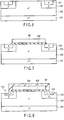
- FIG. 1 is a sectional view showing the configuration of a DIMOSFET according to a first embodiment of the present invention.
- an SiC layer (n - layer) 102 including an n-type impurity concentration of about 5 ⁇ 10 15 to 2x10 16 /cm 3 and having a thickness of about 5 to 10 ⁇ m is formed on a hexagonal SiC substrate (n + substrate) 101 containing an n-type impurity with a concentration of about 5 ⁇ 10 18 to 1 ⁇ 10 19 /cm 3 .
- a first silicon carbide region 103 (p-type well) exists in a region up to a depth of 900 nm from the surface of the SiC layer 102 and is formed so that the concentration of aluminum (Al) as a p-type impurity changes from about 1 ⁇ 10 16 to 2 ⁇ 10 19 /cm 3 (peak concentration) in the depth direction from the surface.
- This p-type well serves as a p-type base region 103.
- An n-type source region 104 is formed as a second silicon carbide region within the p-type base region 103. More specifically, the source region 104 in which the concentration of nitrogen (N) as an n-type impurity changes from about 1 ⁇ 10 18 /cm 3 to 2 ⁇ 10 20 /cm 3 (peak concentration) in the depth direction from the surface exists in a region up to a depth of 500 nm from the surface of the SiC layer 102.
- FIG. 2 shows an n-type impurity distribution in a depth direction in a section along the line A-A in FIG. 1 . This impurity distribution will be described later.
- a trench having a depth of 350 nm is formed in their surfaces, and a source electrode (first electrode) 108 is formed within this trench.
- a gate dielectric 105 having a thickness of about 50 nm is formed across these regions.
- a gate electrode 106 made of polysilicon is formed on the gate dielectric 105.
- a drain electrode (second electrode) 107 is formed on the lower surface of the SiC substrate 101.
- the surface of the p-type base region 103 in direct contact with the gate dielectric 105 is formed to have a relatively low impurity concentration of 1 ⁇ 10 16 /cm 3 as shown in FIG. 2 , but its surface in contact with the source electrode 108, that is, the bottom of the trench is formed to have a relatively high concentration of 1 ⁇ 10 18 /cm 3 . Therefore, the p-type base region 103 can be in ohmic contact with the source electrode 108.
- the surface of the n-type source region 104 in direct contact with the gate dielectric 105 is formed to have a relatively low impurity concentration of 1 ⁇ 10 18 /cm 3 as shown in FIG. 2 , but its surface in contact with the source electrode 108, that is, the bottom of the trench is formed to have a relatively high concentration (n + ) of 2 ⁇ 10 20 /cm 3 . Therefore, the n-type source region 104 can be in ohmic contact with the source electrode 108.
- the gate dielectric 105 in contact with the source region 104 is improved in roughness and crystallinity, which makes it possible to reduce a decrease in inversion channel mobility due to the roughness and improve the reliability of the gate dielectric 105.
- p + ion implantation into the p-type base region 103 which has heretofore been carried out is no longer necessary, leading to a simplified process.
- a defective device is mixed in which the histogram of a gate dielectric breakdown voltage is distributed at 0 to 3 MV/cm due to implantation damage, as shown in FIG. 3 .
- the surface in direct contact with the gate dielectric 105 is formed to have a relatively low impurity concentration of 1 ⁇ 10 18 /cm 3 as shown in FIG. 2 , generation of the defective device is inhibited, the implantation damage is significantly reduced, and the histogram of the gate dielectric breakdown voltage is only distributed at 8 MV/cm or more, thus enabling a gate dielectric of extremely high reliability.
- the impurity concentration of the base region in contact with the gate dielectric is lower than the impurity concentration of the surface of the base region exposed in the trench. Moreover, the impurity concentration of the surface of the source region exposed in the trench is higher than the impurity concentration of the part of the source region in contact with the gate dielectric.
- the concentration of aluminum in the part in contact with the gate dielectric is less than 1 ⁇ 10 17 /cm 3 , and the concentration of aluminum in the surface exposed in the trench is 1 ⁇ 10 17 /cm 3 or more.
- the concentration of phosphorus in the part in contact with the gate dielectric is less than 1 ⁇ 10 19 /cm 3 , and the concentration of phosphorus in the surface exposed in the trench is 1 ⁇ 10 19 /cm 3 or more.
- the highly resistant (n - -type) SiC layer 102 which contains nitrogen (N) as an n-type impurity with a surface impurity concentration of 1 ⁇ 10 16 /cm 3 and which has a thickness of 10 ⁇ m is sequentially formed by an epitaxial growth method on the low resistant 4H-SiC substrate 101 which contains nitrogen as an n-type impurity with an impurity concentration of 1 ⁇ 10 19 /cm 3 and which has a thickness of 300 ⁇ m and which has a hexagonal crystal lattice.
- N nitrogen
- P phosphorus
- SiC layer 102 silicon oxide film
- the surface of the silicon oxide film (not shown) is spin-coated with a resist (not shown), and the resist is patterned by a photolithographic technique.
- the silicon oxide film is subjected to isotropic etching such as RIE.
- an ion implantation mask (not shown) in a later-mentioned ion implantation step is formed.
- Selective Al ion implantation into the SiC layer 102 via the ion implantation mask is carried out.
- the base region 103 containing the p-type impurity is formed in a region of a depth of 900 nm from the surface, as shown in FIG. 5 .
- the source region 104 is selectively formed in the base region 103 by ion implantation.
- an impurity concentration distribution in a direction along the line A-A in FIG. 1 is as shown in FIG. 2 , as described above.
- the implanted impurity is activated by a thermal treatment at about 1600°C.
- the gate dielectric 105 is selectively formed by, for example, the thermal oxidation method or CVD method across the SiC layer 102, the base region 103 and the source region 104.
- the surface of the source region 104 in direct contact with the gate dielectric 105 is formed to have a relatively low impurity concentration of 1 ⁇ 10 18 /cm 3 as described above, and this inhibits surface roughening due to the high-temperature treatment, so that a flat and dense gate dielectric 105 can be formed on the source region 104, thereby enabling a significant improvement in the long-term reliability of the gate dielectric 105.
- the impurity concentration of the surface of the p-type base region 103 in direct contact with the gate dielectric 105 is also 1 ⁇ 10 18 /cm 3 .
- a polysilicon layer is formed on the gate dielectric 105 by the CVD method, and the polysilicon layer is patterned by lithography or the RIE method to form the gate electrode 106.
- a resist 109 covering the gate electrode 106 is formed, and using the resist 109 as a mask, a trench 110 is formed in the surfaces of the n-type source region 104 and the p-type base region 103 by isotropic etching such as RIE.
- the n-type source region exposed in the bottom of the trench is an n + type with an impurity concentration of 2 ⁇ 10 20 /cm 3 , and forms a satisfactory ohmic contact with the source electrode to be formed later.
- an Ni film is formed on the source region 104 by vapor deposition, and the source electrode 108 is selectively formed by a liftoff method. Further, the drain electrode 107 is also formed on the rear surface by the vapor deposition of an Ni film. Finally, a sinter treatment is performed at 950°C for about five minutes to provide a satisfactory ohmic contact between the source electrode 108 and the drain electrode 107. Consequently, the DIMOSFET in the first embodiment shown in FIG. 1 is completed.
- the n-type impurity is formed with a relatively low concentration in a relevant part within the source region in direct contact with the gate dielectric, such that surface roughening on the source region due to a high-temperature treatment of about 1600°C is inhibited, and the flat and dense gate dielectric can be obtained on this region, and moreover, the reliability of the gate dielectric can be improved to a great extent.
- the source region in direct contact with the gate dielectric is formed by the conventional method as shown in FIG. 3
- a defective product is generated in which the histogram of the gate dielectric breakdown voltage is distributed at 0 to 3 MV/cm due to implantation damage.
- the source region is formed by the method in the present embodiment, the implantation damage is significantly reduced, and the generation of the defective product is inhibited, such that the histogram of the gate dielectric breakdown voltage is only distributed at 8 MV/cm or more, thus enabling a gate electrode of extremely high reliability.
- FIG. 10 is an impurity concentration profile where the impurity implantation energy in the p-type base region is increased so that the surface may be a p - type while an internal peak concentration is further increased.
- Al as the p-type impurity is set at a dose of 5 ⁇ 10 14 /cm 2 , a peak concentration of 2 ⁇ 10 19 /cm 3 and a surface concentration of 1 ⁇ 10 16 /cm 3 , and phosphorus as an n-type impurity in the source region is set at a dose amount of 4 ⁇ 10 15 /cm 2 , a peak concentration of 2 ⁇ 10 20 /cm 3 and a surface concentration of 1 ⁇ 10 17 /cm 3 , and the depth of the trench is set at 600 nm.
- high trench surface concentrations of 2 ⁇ 10 18 /cm 3 and 2 ⁇ 10 20 /cm 3 are achieved for the respective regions when punch-through is inhibited and the trench is dug to provide a contact between the p-type base region and the n-type source region, so that contact resistance can be reduced.
- the impurity (phosphorus) concentration of the uppermost surface (surface in contact with the gate dielectric) of the n-type source region is reduced to 1 ⁇ 10 17 /cm 3 , such that the reliability and breakdown yield of the gate dielectric are further improved.
- the surface p - -concentration can be controlled by controlling the amount of Al ion implanted into the p-type base region 103 or by counter-doping with, for example, nitrogen to obtain a desired threshold voltage. In that case, the amount of Al ion implanted into the p-type base region 103 can be further increased, and the p-type contact resistance of the trench can be further reduced.
- an application to an IGBT is described as a second modification.
- the IGBT it is only necessary to change the SiC substrate to a p + -type substrate 111, and epitaxially grow the n - -type SiC layer 102 via an n-type layer 112, as shown in FIG. 11 .
- the n-type source region is provided with a gradient in which the concentration increases in the depth direction, and the gate dielectric is therefore formed on a low-concentration region, such that it is possible to expect an improvement in the reliability of the gate dielectric, a decrease in gate leak, and an improvement in breakdown yield.
- the source electrode is provided so that it is embedded in the trench provided in the surface of the part where the n-type source region adjoins the p-type base region, the source electrode can be in contact with the high-concentration portions of the n-type source region and the p-type base region, thereby enabling a low on-resistance both in the n-type region and the p-type region.
- the semiconductor device in the present embodiment does not require the formation of the conventionally formed p + -type region for contact with the p-type base region, and is therefore simple in configuration, easy to manufacture and advantageous for miniaturization. Moreover, no new mask is needed in the lithographic step of the conventional DIMOSFET to obtain the structure in the present embodiment, and in this respect as well, the semiconductor device in the present embodiment is easy to manufacture and advantageous for miniaturization.
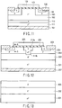
- FIG. 12 is a sectional view showing the configuration of a DIMOSFET according to a second embodiment of the present invention.
- an SiC layer (n - layer) 202 including an n-type impurity concentration of about 5 ⁇ 10 15 to 2 ⁇ 10 16 /cm 3 and having a thickness of about 5 to 10 ⁇ m is formed on a hexagonal 4H-SiC substrate (n + substrate) 201 containing an n-type impurity with a concentration of about 5 ⁇ 10 18 to 1 ⁇ 10 19 /cm 3 .
- a p-type base layer 203 is formed with a thickness of 900 nm so that the concentration of aluminum (Al) as a p-type impurity changes from about 1 ⁇ 10 16 /cm 3 to 2 ⁇ 10 19 /cm 3 (peak concentration) in the depth direction from the surface.
- n-type source region 204 of a depth of 450 nm and an n-type region 214a which is formed on the same level as the source region 204, and there is further formed a contact 241b for connecting the n-type SiC layer 202 to the n-type region 214a.
- Nitrogen (N) is added as an n-type impurity to the n-type source region 204 and the n-type region 214a, and the concentration changes from about 1 ⁇ 10 18 /cm 3 to 2 ⁇ 10 20 /cm 3 (peak concentration) in the depth direction from the surface.
- a depth-direction n-type impurity concentration distribution in a section along the line A-A in FIG. 12 is similar to that in FIG. 2 in the first embodiment.
- a trench having a depth of 350 nm is formed in their surfaces, and a source electrode 208 is formed within this trench.
- a gate dielectric 205 having a thickness of about 80 nm is formed across these regions.
- a gate electrode 206 made of polysilicon is formed on the gate dielectric 205.
- a drain electrode 207 is formed on the lower surface of the SiC substrate 201.
- the surface of the p-type base layer 203 in direct contact with the gate dielectric 205 is formed to have a relatively low impurity concentration of 1 ⁇ 10 16 /cm 3 , but its surface in contact with the source electrode 208, that is, the bottom of the trench is formed to have a relatively high concentration of 1 ⁇ 10 18 /cm 3 . Therefore, the p-type base layer 203 can be in ohmic contact with the source electrode 208.
- the surface of the n-type source region 204 in direct contact with the gate dielectric 205 is formed to have a relatively low impurity concentration of 1 ⁇ 10 18 /cm 3 , but its surface in contact with the source electrode 208, that is, the bottom of the trench is formed to have a relatively high concentration (n + ) of 2 ⁇ 10 20 /cm 3 . Therefore, the n-type source region 204 can be in ohmic contact with the source electrode 208.
- the gate dielectric 205 in contact with the source region 204 is improved in roughness and crystallinity, which makes it possible to reduce a decrease in mobility caused by an inversion channel due to the roughness and improve the reliability of the gate dielectric 205.
- p + ion implantation into the p-type base layer 203, which has heretofore been carried out, is no longer necessary, leading to a simplified process.
- the n-type region 214a connected to the drift layer 202 is formed in the surface of the p-type base layer 203 at the same time as the formation of the source region 204 using a single mask, and a fixed length of a channel region can be formed. This enables a MOSFET to have uniform characteristics.
- the highly resistant (n - -type) SiC layer 202 which contains nitrogen (N) as an n-type impurity with a surface impurity concentration of about 1 ⁇ 10 16 /cm 3 and which has a thickness of 10 ⁇ m is formed by the epitaxial growth method on the low resistant 4H-SiC substrate 201 which contains nitrogen as an n-type impurity with an impurity concentration of 1 ⁇ 10 19 /cm 3 and which has a thickness of 300 ⁇ m and which has a hexagonal crystal lattice.
- nitrogen (N) is used as the n-type impurity here, other impurities such as phosphorus (P) may be used.
- nitrogen and phosphorus may be used in combination.
- Al ion implantation into the SiC layer 202 is carried out.
- substrate temperature Tsub room temperature to 500°C, here, room temperature
- acceleration energy Eacc 600 keV
- total dose ⁇ 2.5 ⁇ 10 14 /cm 2 .
- the base layer 203 containing the p-type impurity is formed, as shown in FIG. 13 .
- the source region 204 and the n-type region 214a are selectively formed in the base layer 203 at the same time by ion implantation.
- the phosphorus (P) ion implantation is carried out with the substrate heated to a temperature of about 600°C under conditions including an acceleration energy of 400 keV and a total dose of 3 ⁇ 10 15 /cm 2 .
- an impurity concentration distribution in a direction along the line A-A in FIG. 14 is as shown in FIG. 2 , as described above.
- the implanted impurity is activated by a thermal treatment at about 1600°C.
- an n + -type contact 214b connecting the n-type region 214a to the drift layer 202 is formed by phosphorus (P) ion implantation.
- the gate dielectric 205 is selectively formed by, for example, the thermal oxidation method or CVD method across the source region 204, the base layer 203 and the n-type region 214a.
- the surface of the source region 204 in direct contact with the gate dielectric 205 is formed to have a relatively low impurity concentration of 1 ⁇ 10 18 /cm 3 as described above, and this inhibits surface roughening due to the high-temperature treatment, so that a flat and dense gate dielectric 205 can be formed on the source region 204, thereby enabling a significant improvement in the long-term reliability of the gate dielectric 205.
- the impurity concentration of the surface of the p-type base layer 203 in contact with the gate dielectric 205 is also 1 ⁇ 10 18 /cm 3 .
- a polysilicon layer is formed on the gate dielectric 205 by the CVD method, and the polysilicon layer is patterned by lithography or the RIE method to form the gate electrode 206.
- a resist 209 covering the gate electrode 206 is formed, and using the resist 209 as a mask, a trench 210 is formed in the surfaces of the n-type source region 204 and the p-type base layer 203 by isotropic etching such as RIE.
- the n-type source region exposed in the bottom of the trench is an n + type with an impurity concentration of about 2 ⁇ 10 20 /cm 3 , and forms a satisfactory ohmic contact with the source electrode to be formed later.
- an Ni film is formed on the entire surface by vapor deposition, and the source electrode 208 is selectively formed by the liftoff method. Further, the drain electrode 207 is also formed on the rear surface by the vapor deposition of an Ni film. Finally, a sinter treatment is performed at 950°C for about five minutes to provide a satisfactory ohmic contact between the source electrode 208 and the drain electrode 207. Consequently, the DIMOSFET in the second embodiment shown in FIG. 12 is completed.
- the n-type impurity is formed with a relatively low concentration in a relevant part within the source region 204 in direct contact with the gate dielectric 205, such that surface roughening on the source region due to a high-temperature treatment of about 1600°C is inhibited, and a flat and dense gate dielectric can be obtained on this region, and moreover, the reliability of the gate dielectric 205 can be improved to a great extent.
- the n-type region 214a connected to the drift layer 202 is formed in the surface of the p-type base layer 203 with the same mask as the source region 204, and a channel region of fixed length can-be formed. This enables the MOSFET to have uniform characteristics.
- an IGBT can be formed as in the first embodiment if a p-type base substrate is formed.
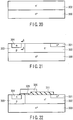
- FIG. 19 is a sectional view showing the configuration of a horizontal DIMOSFET according to a third embodiment of the present invention.
- This DIMOSFET may be basically considered to be a horizontal type of the DIMOSFET in the first embodiment.
- a p-type base region 303 and a source region 304 formed therein are selectively formed at the upper left of an n-type silicon carbide substrate 300 (N) to which nitrogen is added, as in the first embodiment.
- N n-type silicon carbide substrate 300
- N Adjacently to the p-type base region 303, a low-concentration third silicon carbide region 302 (N) to which nitrogen is added is formed on the silicon carbide substrate 300.
- the p-type base region 303 is formed with a thickness of 900 nm so that the concentration of aluminum (Al) as a p-type impurity changes from about 1 ⁇ 10 16 /cm 3 to 2 ⁇ 10 19 /cm 3 (peak concentration) in the depth direction from the surface.
- the n-type source region 304 is formed with a depth of 500 nm so that the concentration of nitrogen (N) as an n-type impurity changes from about 1 ⁇ 10 18 /cm 3 to 2 ⁇ 10 20 /cm 3 (peak concentration) in the depth direction from the surface.
- N nitrogen
- a depth-direction n-type impurity concentration distribution in a section along the A-A line in FIG. 19 is similar to that in FIG. 2 .
- a trench having a depth of 350 nm is formed in their surfaces, and a source electrode (first electrode) 308 is formed within this trench.
- a gate dielectric 305 having a thickness of about 50 nm is formed across these regions.
- a gate electrode 306 made of polysilicon is formed on the gate dielectric 305.
- an n-type drain region 301 to which P is added is formed separately from the p-type base region 303, on which a drain electrode (second electrode) 307 is formed.
- the upper surfaces of the n-type region 302 and the drain region 301 are selectively covered with a dielectric 311.
- the highly resistant (n - -type) SiC layer 302 which contains nitrogen (N) as an n-type impurity with a surface impurity concentration of 1 ⁇ 10 16 /cm 3 and which has a thickness of 600 nm is sequentially formed by the epitaxial growth method on the low resistant 4H-SiC substrate 300 which contains nitrogen as an n-type impurity and which has a thickness of about 300 ⁇ m and which has a hexagonal crystal lattice.
- Al ion implantation into the SiC layer 302 is carried out.
- substrate temperature Tsub room temperature to 600°C, here, room temperature
- acceleration energy Eacc 600 keV
- total dose ⁇ 2.5 ⁇ 10 14 /cm 2 .
- the base region 303 containing the p-type impurity is formed.
- the source region 304 is selectively formed in the base region 303 by ion implantation.
- phosphorus (P) ion implantation is carried out with the substrate heated to a temperature of about 600°C under conditions including an acceleration energy of 400 keV and a total dose of 3 ⁇ 10 15 /cm 2 .
- an impurity concentration distribution in a direction along the line A-A in FIG. 20 is as shown in FIG. 2 , as described above.
- the implanted impurity is activated by a thermal treatment at about 1600°C.
- the n + -type drain region 301 is formed in the n-type region 302 separately from the p-type base layer.
- the gate dielectric 305 is selectively formed by, for example, the thermal oxidation method or CVD method across the SiC layer 302, the base region 303 and the source region 304. Further, the dielectric 311 is selectively formed partly on the upper surface of the SiC region 302 and the upper surface of the drain region 301.
- the surface of the source region 304 in direct contact with the gate dielectric 305 is formed to have a relatively low impurity concentration of 1 ⁇ 10 18 /cm 3 as described above, and this inhibits surface roughening due to the high-temperature treatment, so that a flat and dense gate dielectric 305 can be formed on the source region 304, thereby enabling a significant improvement in the long-term reliability of the gate dielectric 305.
- the impurity concentration of the surface of the p-type base region 303 in contact with the gate dielectric 305 is also 1 ⁇ 10 18 /cm 3 .
- a polysilicon layer is formed on the gate dielectric 305 by the CVD method, and the polysilicon layer is patterned by lithography or the RIE method to form the gate electrode 306.
- a resist 309 covering the gate electrode 306 is formed, and using the resist 309 as a mask, a trench 310 is formed in the surfaces of the n-type source region 304 and the p-type base region 303 by isotropic etching such as RIE.
- the n-type source region exposed in the bottom of the trench is an n + type with an impurity concentration of about 2 ⁇ 10 20 /cm 3 , and forms a satisfactory ohmic contact with the source electrode to be formed later.
- an Ni film 312 is formed on the entire surface by vapor deposition after the resist mask 309 on the drain region 301 has been removed, and the source electrode 308 and the drain electrode 307 are selectively formed by the liftoff method. Finally, a sinter treatment is performed at 950°C for about five minutes to provide the source electrode 308 and the drain electrode 307 with a satisfactory ohmic contact. Consequently, the horizontal DIMOSFET in the third embodiment shown in FIG. 19 is completed.
- the n-type impurity is formed with a relatively low concentration in a relevant part within the source region 304 in direct contact with the gate dielectric 305 as in the first embodiment, such that surface roughening on the source region due to a high-temperature treatment of about 1600°C is inhibited, and a flat and dense gate dielectric can be obtained on this region, and moreover, the reliability of the gate dielectric 305 can be improved to a great extent.
Landscapes
- Electrodes Of Semiconductors (AREA)
- Insulated Gate Type Field-Effect Transistor (AREA)
Claims (7)
- Halbleitervorrichtung, umfassend:ein Siliciumcarbidsubstrat (101) eines ersten Leitfähigkeitstyps oder eines zweiten Leitfähigkeitstyps mit einer ersten Hauptoberfläche und einer zweiten Hauptoberfläche, die einander gegenüberliegen;eine Siliciumcarbidschicht (102) des ersten Leitfähigkeitstyps, die auf der ersten Hauptoberfläche des Siliciumcarbidsubstrats (101) ausgebildet ist;einen ersten Siliciumcarbidbereich (103) des zweiten Leitfähigkeitstyps, der innerhalb einer Oberfläche der Siliciumcarbidschicht (102) ausgebildet ist;einen zweiten Siliciumcarbidbereich (104) des ersten Leitfähigkeitstyps, der innerhalb einer Oberfläche des ersten Siliciumcarbidbereichs (103) ausgebildet ist;ein Gate-Dielektrikum (105), das kontinuierlich auf der Siliciumcarbidschicht (102), dem zweiten Siliciumcarbidbereich (104) und der Oberfläche des ersten Siliciumcarbidbereichs (103) ausgebildet ist, der zwischen der Siliciumcarbidschicht (102) und dem zweiten Siliciumcarbidbereich (104) eingefügt ist;eine Gate-Elektrode (106), die auf dem Gate-Dielektrikum (105) ausgebildet ist;eine erste Elektrode (108), die in einem Graben eingebettet ist, der selektiv in einem Bereich ausgebildet ist, in dem der erste Siliciumcarbidbereich (103) an den zweiten Siliciumcarbidbereich (104) an der unteren Oberfläche des Grabens angrenzt; undeine zweite Elektrode (107), die auf der zweiten Hauptoberfläche des Siliciumcarbidsubstrats (101) ausgebildet ist,dadurch gekennzeichnet, dass eine Verunreinigungskonzentration in einem Teil des ersten Siliciumcarbidbereichs (103) in Kontakt mit dem Gate-Dielektrikum (105) niedriger ist als diejenige des ersten Siliciumcarbidbereichs (103) an einer unteren Oberfläche des Grabens, und die Verunreinigungskonzentration in einem Teil des zweiten Siliciumcarbidbereichs (104) in Kontakt mit dem Gate-Dielektrikum (105) niedriger ist als diejenige des zweiten Siliciumcarbidbereichs (104) an der unteren Oberfläche des Grabens.
- Halbleitervorrichtung, umfassend:ein Siliciumcarbidsubstrat (201) eines ersten Leitfähigkeitstyps oder eines zweiten Leitfähigkeitstyps mit einer ersten Hauptoberfläche und einer zweiten Hauptoberfläche, die einander gegenüberliegen;eine Siliciumcarbidschicht (202) des ersten Leitfähigkeitstyps, die auf der ersten Hauptoberfläche des Siliciumcarbidsubstrats (201) ausgebildet ist;einen ersten Siliciumcarbidbereich (203) des zweiten Leitfähigkeitstyps, der auf einer Oberfläche der Siliciumcarbidschicht (202) ausgebildet ist;einen zweiten Siliciumcarbidbereich (204) des ersten Leitfähigkeitstyps, der innerhalb einer Oberfläche des ersten Siliciumcarbidbereichs (203) ausgebildet ist;einen dritten Siliciumcarbidbereich (214a) des ersten Leitfähigkeitstyps, der getrennt vom zweiten Siliciumcarbidbereich (204) innerhalb einer Oberfläche des ersten Siliciumcarbidbereichs (203) ausgebildet ist und dieselbe Tiefe und dieselbe Verunreinigungskonzentrationsverteilung wie der zweite Siliciumcarbidbereich (204) aufweist; undeinen vierten Siliciumcarbidbereich (214b) des ersten Leitfähigkeitstyps, der den dritten Siliciumcarbidbereich (214a) mit der Siliciumcarbidschicht (202) verbindet;ein Gate-Dielektrikum (205), das kontinuierlich auf dem zweiten Siliciumcarbidbereich (204), der Oberfläche des ersten Siliciumcarbidbereichs (203) und des dritten Siliciumcarbidbereichs (214a) ausgebildet ist;eine Gate-Elektrode (206), die auf dem Gate-Dielektrikum (205) ausgebildet ist;eine erste Elektrode (208), die in einem Graben eingebettet ist, der selektiv in einem Bereich ausgebildet ist, in dem der erste Siliciumcarbidbereich (203) an den zweiten Siliciumcarbidbereich (204) an der unteren Oberfläche des Grabens angrenzt; undeine zweite Elektrode (207), die auf der zweiten Hauptoberfläche des Siliciumcarbidsubstrats (201) ausgebildet ist,dadurch gekennzeichnet, dass eine Verunreinigungskonzentration in einem Teil des ersten Siliciumcarbidbereichs (203) in Kontakt mit dem Gate-Dielektrikum (205) niedriger ist als diejenige des ersten Siliciumcarbidbereichs (203) an einer unteren Oberfläche des Grabens, und die Verunreinigungskonzentration in einem Teil des zweiten Siliciumcarbidbereichs (204) in Kontakt mit dem Gate-Dielektrikum (205) niedriger ist als diejenige des zweiten Siliciumcarbidbereichs (204) an der unteren Oberfläche des Grabens.
- Halbleitervorrichtung, umfassend:ein Siliciumcarbidsubstrat (300);einen ersten Siliciumcarbidbereich (303) eines zweiten Leitfähigkeitstyps, der auf einer oberen Oberfläche des Siliciumcarbidsubstrats (300) ausgebildet ist;einen zweiten Siliciumcarbidbereich (304) eines ersten Leitfähigkeitstyps, der innerhalb einer oberen Oberfläche des ersten Siliciumcarbidbereichs (303) ausgebildet ist;einen dritten Siliciumcarbidbereich (302) des ersten Leitfähigkeitstyps, der auf der oberen Oberfläche des Siliciumcarbidsubstrats (300) und benachbart zum ersten Siliciumcarbidbereich (303) ausgebildet ist;einen vierten Siliciumcarbidbereich (301) des ersten Leitfähigkeitstyps, der getrennt vom ersten Siliciumcarbidbereich (303) auf der oberen Oberfläche des dritten Siliciumcarbidbereichs (302) ausgebildet ist;ein Gate-Dielektrikum (305), das kontinuierlich auf dem dritten Siliciumcarbidbereich (302), dem zweiten Siliciumcarbidbereich (304) und der oberen Oberfläche des ersten Siliciumcarbidbereichs (303) ausgebildet ist, der zwischen dem dritten Siliciumcarbidbereich (302) und dem zweiten Siliciumcarbidbereich (304) eingefügt ist;eine Gate-Elektrode (306), die auf dem Gate-Dielektrikum (305) ausgebildet ist;eine erste Elektrode (308), die in einem Graben eingebettet ist, der selektiv in einem Bereich ausgebildet ist, in dem der erste Siliciumcarbidbereich (303) an den zweiten Siliciumcarbidbereich (304) an der unteren Oberfläche des Grabens angrenzt; undeine zweite Elektrode (307), die auf einer oberen Oberfläche des vierten Siliciumcarbidbereichs (301) ausgebildet ist,dadurch gekennzeichnet, dass eine Verunreinigungskonzentration in einem Teil des ersten Siliciumcarbidbereichs (303) in Kontakt mit dem Gate-Dielektrikum (305) niedriger ist als diejenige des ersten Siliciumcarbidbereichs (303) an einem teilweisen Kontakt mit einer unteren Oberfläche des Grabens, und die Verunreinigungskonzentration in einem Teil des zweiten Siliciumcarbidbereichs (304) in Kontakt mit dem Gate-Dielektrikum (305) niedriger ist als diejenige des zweiten Siliciumcarbidbereichs (304) an einem teilweisen Kontakt mit der unteren Oberfläche des Grabens.
- Halbleitervorrichtung nach einem der Ansprüche 1, 2 und 3, dadurch gekennzeichnet, dass der erste Siliciumcarbidbereich (103, 203, 303) Aluminium als eine Verunreinigung enthält und eine Aluminiumkonzentration in einem Teil des ersten Siliciumcarbidbereichs (103, 203, 303) in Kontakt mit dem Gate-Dielektrikum (105, 205, 305) kleiner als 1×10¹⁷/cm3 ist.
- Halbleitervorrichtung nach einem der Ansprüche 1, 2 und 3, dadurch gekennzeichnet, dass der zweite Siliciumcarbidbereich (104, 204, 304) Phosphor als eine Verunreinigung enthält und eine Phosphorkonzentration in einem Teil des zweiten Siliciumcarbidbereichs (104, 204, 304) in Kontakt mit dem Gate-Dielektrikum geringer als 1×10¹⁹/cm3 ist.
- Halbleitervorrichtung nach einem der Ansprüche 1, 2 und 3, dadurch gekennzeichnet, dass der erste Siliciumcarbidbereich (103, 203, 303) Aluminium als eine Verunreinigung enthält und eine Aluminiumkonzentration im ersten Siliciumcarbidbereich (103, 203, 303) an einer unteren Oberfläche des Grabens 1×10¹⁷/cm3 oder höher ist.
- Halbleitervorrichtung nach einem der Ansprüche 1, 2 und 3, dadurch gekennzeichnet, dass der zweite Siliciumcarbidbereich (104, 204, 304) Phosphor als eine Verunreinigung enthält und eine Phosphorkonzentration in einer Oberfläche des zweiten Siliciumcarbidbereichs (104, 204, 304), die der ersten Elektrode (108, 208, 308) zugewandt ist, 1×10¹⁹/cm3 oder höher ist.
Applications Claiming Priority (2)
| Application Number | Priority Date | Filing Date | Title |
|---|---|---|---|
| JP2008022001A JP2009182271A (ja) | 2008-01-31 | 2008-01-31 | 炭化珪素半導体装置 |
| PCT/JP2009/050789 WO2009096269A1 (en) | 2008-01-31 | 2009-01-14 | Silicon carbide semiconductor device |
Publications (2)
| Publication Number | Publication Date |
|---|---|
| EP2248178A1 EP2248178A1 (de) | 2010-11-10 |
| EP2248178B1 true EP2248178B1 (de) | 2018-10-10 |
Family
ID=40473531
Family Applications (1)
| Application Number | Title | Priority Date | Filing Date |
|---|---|---|---|
| EP09706248.3A Active EP2248178B1 (de) | 2008-01-31 | 2009-01-14 | Halbleiterbauelement aus siliziumkarbid |
Country Status (5)
| Country | Link |
|---|---|
| US (1) | US8431974B2 (de) |
| EP (1) | EP2248178B1 (de) |
| JP (1) | JP2009182271A (de) |
| CN (1) | CN101933146B (de) |
| WO (1) | WO2009096269A1 (de) |
Families Citing this family (35)
| Publication number | Priority date | Publication date | Assignee | Title |
|---|---|---|---|---|
| JP5408248B2 (ja) * | 2009-05-20 | 2014-02-05 | 三菱電機株式会社 | 炭化珪素半導体装置およびその製造方法 |
| JP5474068B2 (ja) * | 2009-07-24 | 2014-04-16 | 三菱電機株式会社 | 炭化珪素半導体装置の製造方法 |
| JP2011060901A (ja) * | 2009-09-08 | 2011-03-24 | Sumitomo Electric Ind Ltd | 半導体装置および半導体装置の製造方法 |
| JP5732790B2 (ja) | 2010-09-14 | 2015-06-10 | 株式会社デンソー | 炭化珪素半導体装置およびその製造方法 |
| JP2012064873A (ja) * | 2010-09-17 | 2012-03-29 | Rohm Co Ltd | 半導体装置およびその製造方法 |
| US8373215B2 (en) * | 2010-10-25 | 2013-02-12 | Texas Instruments Incorporated | Zero temperature coefficient capacitor |
| JP5954856B2 (ja) | 2011-02-01 | 2016-07-20 | ルネサスエレクトロニクス株式会社 | 縦チャネル型ノーマリオフ型パワーjfetの製造方法 |
| JP5687127B2 (ja) * | 2011-05-06 | 2015-03-18 | 三菱電機株式会社 | 半導体装置およびその製造方法 |
| JP5687128B2 (ja) * | 2011-05-06 | 2015-03-18 | 三菱電機株式会社 | 半導体装置およびその製造方法 |
| JP5797266B2 (ja) * | 2011-06-14 | 2015-10-21 | 三菱電機株式会社 | 炭化珪素半導体装置及び炭化珪素半導体装置の製造方法 |
| DE112011105633T5 (de) * | 2011-09-21 | 2014-08-28 | Mitsubishi Electric Corp. | Siliziumkarbidhalbleitervorrichtung und Verfahren zu ihrer Herstellung |
| JP5875334B2 (ja) * | 2011-11-11 | 2016-03-02 | 株式会社日立製作所 | 炭化珪素半導体装置 |
| CN102544104A (zh) * | 2012-01-12 | 2012-07-04 | 清华大学 | 一种耐高压的隧穿晶体管及其制备方法 |
| WO2014021365A1 (ja) * | 2012-07-31 | 2014-02-06 | 独立行政法人産業技術総合研究所 | 半導体構造物、半導体装置及び該半導体構造物の製造方法 |
| JP5792701B2 (ja) | 2012-09-24 | 2015-10-14 | 株式会社東芝 | 半導体装置及びその製造方法 |
| JP6018501B2 (ja) * | 2012-12-27 | 2016-11-02 | 株式会社東芝 | 半導体装置及びその製造方法 |
| JP6219044B2 (ja) | 2013-03-22 | 2017-10-25 | 株式会社東芝 | 半導体装置およびその製造方法 |
| CN103681256B (zh) * | 2013-08-27 | 2016-12-07 | 厦门天睿电子有限公司 | 一种碳化硅mosfet器件及其制作方法 |
| JP5928429B2 (ja) | 2013-09-30 | 2016-06-01 | サンケン電気株式会社 | 半導体装置及びその製造方法 |
| JP2016004955A (ja) * | 2014-06-19 | 2016-01-12 | 三菱電機株式会社 | 炭化珪素半導体装置及びその製造方法 |
| JP6277902B2 (ja) * | 2014-07-24 | 2018-02-14 | 富士電機株式会社 | 半導体装置及び半導体装置の製造方法 |
| JP2015057851A (ja) * | 2014-11-19 | 2015-03-26 | 三菱電機株式会社 | 半導体装置 |
| JP6476821B2 (ja) * | 2014-12-16 | 2019-03-06 | 富士電機株式会社 | 縦型mosfetおよび縦型mosfetの製造方法 |
| JP2016143788A (ja) * | 2015-02-03 | 2016-08-08 | 住友電気工業株式会社 | 炭化珪素半導体装置の製造方法 |
| JP6610653B2 (ja) * | 2015-02-20 | 2019-11-27 | 住友電気工業株式会社 | 炭化珪素半導体装置 |
| JP2015156506A (ja) * | 2015-04-10 | 2015-08-27 | 三菱電機株式会社 | 炭化珪素半導体装置およびその製造方法 |
| JP2016213419A (ja) * | 2015-05-13 | 2016-12-15 | 住友電気工業株式会社 | 炭化珪素半導体装置 |
| US20180145130A1 (en) * | 2016-05-17 | 2018-05-24 | Littelfuse, Inc. | Igbt with improved reverse blocking capability |
| JP6289600B2 (ja) * | 2016-12-22 | 2018-03-07 | 三菱電機株式会社 | 半導体装置 |
| CN108695387B (zh) * | 2017-04-12 | 2021-07-16 | 比亚迪半导体股份有限公司 | Mosfet、mosfet制备方法以及电子设备 |
| US11380763B2 (en) * | 2019-04-29 | 2022-07-05 | Arizona Board Of Regents On Behalf Of Arizona State University | Contact structures for n-type diamond |
| GB201909588D0 (en) * | 2019-07-03 | 2019-08-14 | Univ Coventry | A semiconductor device and methods for production thereof |
| JP7370309B2 (ja) * | 2020-10-21 | 2023-10-27 | 三菱電機株式会社 | 逆導通型半導体装置および逆導通型半導体装置の製造方法 |
| CN119836857A (zh) * | 2023-07-18 | 2025-04-15 | 株式会社东芝 | 半导体装置 |
| JP2025049727A (ja) * | 2023-09-22 | 2025-04-04 | 株式会社東芝 | 半導体装置 |
Family Cites Families (14)
| Publication number | Priority date | Publication date | Assignee | Title |
|---|---|---|---|---|
| JP3385938B2 (ja) * | 1997-03-05 | 2003-03-10 | 株式会社デンソー | 炭化珪素半導体装置及びその製造方法 |
| US6121633A (en) * | 1997-06-12 | 2000-09-19 | Cree Research, Inc. | Latch-up free power MOS-bipolar transistor |
| JP3180895B2 (ja) * | 1997-08-18 | 2001-06-25 | 富士電機株式会社 | 炭化けい素半導体装置の製造方法 |
| US6246076B1 (en) * | 1998-08-28 | 2001-06-12 | Cree, Inc. | Layered dielectric on silicon carbide semiconductor structures |
| US6724039B1 (en) | 1998-08-31 | 2004-04-20 | Stmicroelectronics, Inc. | Semiconductor device having a Schottky diode |
| JP3551909B2 (ja) * | 1999-11-18 | 2004-08-11 | 株式会社デンソー | 炭化珪素半導体装置の製造方法 |
| JP4848607B2 (ja) * | 2001-09-11 | 2011-12-28 | 株式会社デンソー | 炭化珪素半導体装置の製造方法 |
| JP4188637B2 (ja) | 2002-08-05 | 2008-11-26 | 独立行政法人産業技術総合研究所 | 半導体装置 |
| US7221010B2 (en) * | 2002-12-20 | 2007-05-22 | Cree, Inc. | Vertical JFET limited silicon carbide power metal-oxide semiconductor field effect transistors |
| JP4635470B2 (ja) * | 2004-04-19 | 2011-02-23 | 株式会社デンソー | 炭化珪素半導体装置およびその製造方法 |
| US7569900B2 (en) * | 2004-11-16 | 2009-08-04 | Kabushiki Kaisha Toshiba | Silicon carbide high breakdown voltage semiconductor device |
| US20080017897A1 (en) | 2006-01-30 | 2008-01-24 | Kabushiki Kaisha Toshiba | Semiconductor device and method of manufacturing same |
| JP2007207784A (ja) * | 2006-01-30 | 2007-08-16 | Toshiba Corp | 半導体装置 |
| JP4786621B2 (ja) * | 2007-09-20 | 2011-10-05 | 株式会社東芝 | 半導体装置およびその製造方法 |
-
2008
- 2008-01-31 JP JP2008022001A patent/JP2009182271A/ja active Pending
-
2009
- 2009-01-14 CN CN2009801035715A patent/CN101933146B/zh active Active
- 2009-01-14 WO PCT/JP2009/050789 patent/WO2009096269A1/en not_active Ceased
- 2009-01-14 EP EP09706248.3A patent/EP2248178B1/de active Active
-
2010
- 2010-07-29 US US12/846,400 patent/US8431974B2/en active Active
Non-Patent Citations (1)
| Title |
|---|
| None * |
Also Published As
| Publication number | Publication date |
|---|---|
| CN101933146A (zh) | 2010-12-29 |
| US20100308343A1 (en) | 2010-12-09 |
| CN101933146B (zh) | 2012-06-27 |
| EP2248178A1 (de) | 2010-11-10 |
| WO2009096269A1 (en) | 2009-08-06 |
| US8431974B2 (en) | 2013-04-30 |
| JP2009182271A (ja) | 2009-08-13 |
Similar Documents
| Publication | Publication Date | Title |
|---|---|---|
| US8431974B2 (en) | Silicon carbide semiconductor device | |
| EP1759418B1 (de) | Silizium-karbid-bauelemente und deren herstellungsverfahren | |
| US8772788B2 (en) | Semiconductor element and method of manufacturing thereof | |
| US8658503B2 (en) | Semiconductor device and method of fabricating the same | |
| JP6472776B2 (ja) | 炭化珪素半導体装置および炭化珪素半導体装置の製造方法 | |
| US8933466B2 (en) | Semiconductor element | |
| US11309414B2 (en) | Metal oxide semiconductor (MOS) controlled devices and methods of making the same | |
| US7892923B2 (en) | Power field effect transistor and manufacturing method thereof | |
| JP5671779B2 (ja) | エピタキシャルウエハの製造方法および半導体装置の製造方法 | |
| US7569900B2 (en) | Silicon carbide high breakdown voltage semiconductor device | |
| US20180308943A1 (en) | Semiconductor device and method for manufacturing the same | |
| JP4595144B2 (ja) | 炭化珪素半導体装置及びその製造方法 | |
| JP4678902B2 (ja) | 炭化けい素umos半導体素子およびその製造方法 | |
| CN116230774A (zh) | 一种非对称碳化硅槽栅mosfet及其制造方法 | |
| CN109478569B (zh) | 碳化硅半导体装置以及碳化硅半导体装置的制造方法 | |
| CA2855304C (en) | Semiconductor devices and methods of manufacture | |
| JP5082853B2 (ja) | Mosfet | |
| JP5684304B2 (ja) | 炭化珪素半導体装置 |
Legal Events
| Date | Code | Title | Description |
|---|---|---|---|
| PUAI | Public reference made under article 153(3) epc to a published international application that has entered the european phase |
Free format text: ORIGINAL CODE: 0009012 |
|
| 17P | Request for examination filed |
Effective date: 20100729 |
|
| AK | Designated contracting states |
Kind code of ref document: A1 Designated state(s): AT BE BG CH CY CZ DE DK EE ES FI FR GB GR HR HU IE IS IT LI LT LU LV MC MK MT NL NO PL PT RO SE SI SK TR |
|
| AX | Request for extension of the european patent |
Extension state: AL BA RS |
|
| DAX | Request for extension of the european patent (deleted) | ||
| 17Q | First examination report despatched |
Effective date: 20130411 |
|
| GRAP | Despatch of communication of intention to grant a patent |
Free format text: ORIGINAL CODE: EPIDOSNIGR1 |
|
| STAA | Information on the status of an ep patent application or granted ep patent |
Free format text: STATUS: GRANT OF PATENT IS INTENDED |
|
| RIC1 | Information provided on ipc code assigned before grant |
Ipc: H01L 21/336 20060101ALI20180614BHEP Ipc: H01L 29/78 20060101AFI20180614BHEP Ipc: H01L 29/423 20060101ALN20180614BHEP Ipc: H01L 29/417 20060101ALI20180614BHEP Ipc: H01L 29/36 20060101ALI20180614BHEP Ipc: H01L 29/16 20060101ALN20180614BHEP Ipc: H01L 21/04 20060101ALI20180614BHEP Ipc: H01L 29/739 20060101ALI20180614BHEP Ipc: H01L 29/45 20060101ALN20180614BHEP |
|
| INTG | Intention to grant announced |
Effective date: 20180627 |
|
| GRAS | Grant fee paid |
Free format text: ORIGINAL CODE: EPIDOSNIGR3 |
|
| GRAA | (expected) grant |
Free format text: ORIGINAL CODE: 0009210 |
|
| STAA | Information on the status of an ep patent application or granted ep patent |
Free format text: STATUS: THE PATENT HAS BEEN GRANTED |
|
| AK | Designated contracting states |
Kind code of ref document: B1 Designated state(s): AT BE BG CH CY CZ DE DK EE ES FI FR GB GR HR HU IE IS IT LI LT LU LV MC MK MT NL NO PL PT RO SE SI SK TR |
|
| REG | Reference to a national code |
Ref country code: GB Ref legal event code: FG4D |
|
| REG | Reference to a national code |
Ref country code: CH Ref legal event code: EP Ref country code: AT Ref legal event code: REF Ref document number: 1052239 Country of ref document: AT Kind code of ref document: T Effective date: 20181015 |
|
| REG | Reference to a national code |
Ref country code: IE Ref legal event code: FG4D |
|
| REG | Reference to a national code |
Ref country code: DE Ref legal event code: R096 Ref document number: 602009054967 Country of ref document: DE |
|
| REG | Reference to a national code |
Ref country code: NL Ref legal event code: MP Effective date: 20181010 |
|
| REG | Reference to a national code |
Ref country code: LT Ref legal event code: MG4D |
|
| REG | Reference to a national code |
Ref country code: AT Ref legal event code: MK05 Ref document number: 1052239 Country of ref document: AT Kind code of ref document: T Effective date: 20181010 |
|
| PG25 | Lapsed in a contracting state [announced via postgrant information from national office to epo] |
Ref country code: NL Free format text: LAPSE BECAUSE OF FAILURE TO SUBMIT A TRANSLATION OF THE DESCRIPTION OR TO PAY THE FEE WITHIN THE PRESCRIBED TIME-LIMIT Effective date: 20181010 |
|
| PG25 | Lapsed in a contracting state [announced via postgrant information from national office to epo] |
Ref country code: LV Free format text: LAPSE BECAUSE OF FAILURE TO SUBMIT A TRANSLATION OF THE DESCRIPTION OR TO PAY THE FEE WITHIN THE PRESCRIBED TIME-LIMIT Effective date: 20181010 Ref country code: AT Free format text: LAPSE BECAUSE OF FAILURE TO SUBMIT A TRANSLATION OF THE DESCRIPTION OR TO PAY THE FEE WITHIN THE PRESCRIBED TIME-LIMIT Effective date: 20181010 Ref country code: NO Free format text: LAPSE BECAUSE OF FAILURE TO SUBMIT A TRANSLATION OF THE DESCRIPTION OR TO PAY THE FEE WITHIN THE PRESCRIBED TIME-LIMIT Effective date: 20190110 Ref country code: LT Free format text: LAPSE BECAUSE OF FAILURE TO SUBMIT A TRANSLATION OF THE DESCRIPTION OR TO PAY THE FEE WITHIN THE PRESCRIBED TIME-LIMIT Effective date: 20181010 Ref country code: PL Free format text: LAPSE BECAUSE OF FAILURE TO SUBMIT A TRANSLATION OF THE DESCRIPTION OR TO PAY THE FEE WITHIN THE PRESCRIBED TIME-LIMIT Effective date: 20181010 Ref country code: HR Free format text: LAPSE BECAUSE OF FAILURE TO SUBMIT A TRANSLATION OF THE DESCRIPTION OR TO PAY THE FEE WITHIN THE PRESCRIBED TIME-LIMIT Effective date: 20181010 Ref country code: ES Free format text: LAPSE BECAUSE OF FAILURE TO SUBMIT A TRANSLATION OF THE DESCRIPTION OR TO PAY THE FEE WITHIN THE PRESCRIBED TIME-LIMIT Effective date: 20181010 Ref country code: BG Free format text: LAPSE BECAUSE OF FAILURE TO SUBMIT A TRANSLATION OF THE DESCRIPTION OR TO PAY THE FEE WITHIN THE PRESCRIBED TIME-LIMIT Effective date: 20190110 Ref country code: IS Free format text: LAPSE BECAUSE OF FAILURE TO SUBMIT A TRANSLATION OF THE DESCRIPTION OR TO PAY THE FEE WITHIN THE PRESCRIBED TIME-LIMIT Effective date: 20190210 Ref country code: FI Free format text: LAPSE BECAUSE OF FAILURE TO SUBMIT A TRANSLATION OF THE DESCRIPTION OR TO PAY THE FEE WITHIN THE PRESCRIBED TIME-LIMIT Effective date: 20181010 |
|
| PG25 | Lapsed in a contracting state [announced via postgrant information from national office to epo] |
Ref country code: GR Free format text: LAPSE BECAUSE OF FAILURE TO SUBMIT A TRANSLATION OF THE DESCRIPTION OR TO PAY THE FEE WITHIN THE PRESCRIBED TIME-LIMIT Effective date: 20190111 Ref country code: SE Free format text: LAPSE BECAUSE OF FAILURE TO SUBMIT A TRANSLATION OF THE DESCRIPTION OR TO PAY THE FEE WITHIN THE PRESCRIBED TIME-LIMIT Effective date: 20181010 Ref country code: PT Free format text: LAPSE BECAUSE OF FAILURE TO SUBMIT A TRANSLATION OF THE DESCRIPTION OR TO PAY THE FEE WITHIN THE PRESCRIBED TIME-LIMIT Effective date: 20190210 |
|
| REG | Reference to a national code |
Ref country code: DE Ref legal event code: R097 Ref document number: 602009054967 Country of ref document: DE |
|
| PG25 | Lapsed in a contracting state [announced via postgrant information from national office to epo] |
Ref country code: DK Free format text: LAPSE BECAUSE OF FAILURE TO SUBMIT A TRANSLATION OF THE DESCRIPTION OR TO PAY THE FEE WITHIN THE PRESCRIBED TIME-LIMIT Effective date: 20181010 Ref country code: IT Free format text: LAPSE BECAUSE OF FAILURE TO SUBMIT A TRANSLATION OF THE DESCRIPTION OR TO PAY THE FEE WITHIN THE PRESCRIBED TIME-LIMIT Effective date: 20181010 Ref country code: CZ Free format text: LAPSE BECAUSE OF FAILURE TO SUBMIT A TRANSLATION OF THE DESCRIPTION OR TO PAY THE FEE WITHIN THE PRESCRIBED TIME-LIMIT Effective date: 20181010 |
|
| PLBE | No opposition filed within time limit |
Free format text: ORIGINAL CODE: 0009261 |
|
| STAA | Information on the status of an ep patent application or granted ep patent |
Free format text: STATUS: NO OPPOSITION FILED WITHIN TIME LIMIT |
|
| PG25 | Lapsed in a contracting state [announced via postgrant information from national office to epo] |
Ref country code: RO Free format text: LAPSE BECAUSE OF FAILURE TO SUBMIT A TRANSLATION OF THE DESCRIPTION OR TO PAY THE FEE WITHIN THE PRESCRIBED TIME-LIMIT Effective date: 20181010 Ref country code: SK Free format text: LAPSE BECAUSE OF FAILURE TO SUBMIT A TRANSLATION OF THE DESCRIPTION OR TO PAY THE FEE WITHIN THE PRESCRIBED TIME-LIMIT Effective date: 20181010 Ref country code: MC Free format text: LAPSE BECAUSE OF FAILURE TO SUBMIT A TRANSLATION OF THE DESCRIPTION OR TO PAY THE FEE WITHIN THE PRESCRIBED TIME-LIMIT Effective date: 20181010 Ref country code: EE Free format text: LAPSE BECAUSE OF FAILURE TO SUBMIT A TRANSLATION OF THE DESCRIPTION OR TO PAY THE FEE WITHIN THE PRESCRIBED TIME-LIMIT Effective date: 20181010 |
|
| REG | Reference to a national code |
Ref country code: CH Ref legal event code: PL |
|
| 26N | No opposition filed |
Effective date: 20190711 |
|
| PG25 | Lapsed in a contracting state [announced via postgrant information from national office to epo] |
Ref country code: LU Free format text: LAPSE BECAUSE OF NON-PAYMENT OF DUE FEES Effective date: 20190114 |
|
| REG | Reference to a national code |
Ref country code: BE Ref legal event code: MM Effective date: 20190131 |
|
| REG | Reference to a national code |
Ref country code: IE Ref legal event code: MM4A |
|
| PG25 | Lapsed in a contracting state [announced via postgrant information from national office to epo] |
Ref country code: SI Free format text: LAPSE BECAUSE OF FAILURE TO SUBMIT A TRANSLATION OF THE DESCRIPTION OR TO PAY THE FEE WITHIN THE PRESCRIBED TIME-LIMIT Effective date: 20181010 |
|
| PG25 | Lapsed in a contracting state [announced via postgrant information from national office to epo] |
Ref country code: BE Free format text: LAPSE BECAUSE OF NON-PAYMENT OF DUE FEES Effective date: 20190131 |
|
| PG25 | Lapsed in a contracting state [announced via postgrant information from national office to epo] |
Ref country code: LI Free format text: LAPSE BECAUSE OF NON-PAYMENT OF DUE FEES Effective date: 20190131 Ref country code: CH Free format text: LAPSE BECAUSE OF NON-PAYMENT OF DUE FEES Effective date: 20190131 |
|
| PG25 | Lapsed in a contracting state [announced via postgrant information from national office to epo] |
Ref country code: IE Free format text: LAPSE BECAUSE OF NON-PAYMENT OF DUE FEES Effective date: 20190114 |
|
| PG25 | Lapsed in a contracting state [announced via postgrant information from national office to epo] |
Ref country code: TR Free format text: LAPSE BECAUSE OF FAILURE TO SUBMIT A TRANSLATION OF THE DESCRIPTION OR TO PAY THE FEE WITHIN THE PRESCRIBED TIME-LIMIT Effective date: 20181010 |
|
| PG25 | Lapsed in a contracting state [announced via postgrant information from national office to epo] |
Ref country code: MT Free format text: LAPSE BECAUSE OF NON-PAYMENT OF DUE FEES Effective date: 20190114 |
|
| PG25 | Lapsed in a contracting state [announced via postgrant information from national office to epo] |
Ref country code: CY Free format text: LAPSE BECAUSE OF FAILURE TO SUBMIT A TRANSLATION OF THE DESCRIPTION OR TO PAY THE FEE WITHIN THE PRESCRIBED TIME-LIMIT Effective date: 20181010 |
|
| PG25 | Lapsed in a contracting state [announced via postgrant information from national office to epo] |
Ref country code: HU Free format text: LAPSE BECAUSE OF FAILURE TO SUBMIT A TRANSLATION OF THE DESCRIPTION OR TO PAY THE FEE WITHIN THE PRESCRIBED TIME-LIMIT; INVALID AB INITIO Effective date: 20090114 |
|
| PG25 | Lapsed in a contracting state [announced via postgrant information from national office to epo] |
Ref country code: MK Free format text: LAPSE BECAUSE OF FAILURE TO SUBMIT A TRANSLATION OF THE DESCRIPTION OR TO PAY THE FEE WITHIN THE PRESCRIBED TIME-LIMIT Effective date: 20181010 |
|
| REG | Reference to a national code |
Ref country code: DE Ref legal event code: R079 Ref document number: 602009054967 Country of ref document: DE Free format text: PREVIOUS MAIN CLASS: H01L0029780000 Ipc: H10D0030600000 |
|
| PGFP | Annual fee paid to national office [announced via postgrant information from national office to epo] |
Ref country code: GB Payment date: 20251127 Year of fee payment: 18 |
|
| PGFP | Annual fee paid to national office [announced via postgrant information from national office to epo] |
Ref country code: FR Payment date: 20251124 Year of fee payment: 18 |
|
| PGFP | Annual fee paid to national office [announced via postgrant information from national office to epo] |
Ref country code: DE Payment date: 20251126 Year of fee payment: 18 |