EP2237319A2 - Dispositif à semi-conducteur et transformateur électrique l'utilisant - Google Patents
Dispositif à semi-conducteur et transformateur électrique l'utilisant Download PDFInfo
- Publication number
- EP2237319A2 EP2237319A2 EP10007172A EP10007172A EP2237319A2 EP 2237319 A2 EP2237319 A2 EP 2237319A2 EP 10007172 A EP10007172 A EP 10007172A EP 10007172 A EP10007172 A EP 10007172A EP 2237319 A2 EP2237319 A2 EP 2237319A2
- Authority
- EP
- European Patent Office
- Prior art keywords
- semiconductor layer
- area
- type
- layer
- neighboring
- Prior art date
- Legal status (The legal status is an assumption and is not a legal conclusion. Google has not performed a legal analysis and makes no representation as to the accuracy of the status listed.)
- Granted
Links
- 239000004065 semiconductor Substances 0.000 claims description 200
- 239000012535 impurity Substances 0.000 claims description 14
- 108091006146 Channels Proteins 0.000 description 25
- 230000000694 effects Effects 0.000 description 11
- 230000005684 electric field Effects 0.000 description 5
- 230000006378 damage Effects 0.000 description 4
- 229910052751 metal Inorganic materials 0.000 description 4
- 239000002184 metal Substances 0.000 description 4
- 238000004519 manufacturing process Methods 0.000 description 3
- 102000004129 N-Type Calcium Channels Human genes 0.000 description 2
- 108090000699 N-Type Calcium Channels Proteins 0.000 description 2
- 238000010586 diagram Methods 0.000 description 2
- 230000005764 inhibitory process Effects 0.000 description 2
- 238000002347 injection Methods 0.000 description 2
- 239000007924 injection Substances 0.000 description 2
- 239000007787 solid Substances 0.000 description 2
- ZOKXTWBITQBERF-UHFFFAOYSA-N Molybdenum Chemical compound [Mo] ZOKXTWBITQBERF-UHFFFAOYSA-N 0.000 description 1
- 238000009825 accumulation Methods 0.000 description 1
- 239000004020 conductor Substances 0.000 description 1
- 238000009792 diffusion process Methods 0.000 description 1
- 230000001771 impaired effect Effects 0.000 description 1
- 230000006698 induction Effects 0.000 description 1
- 238000009413 insulation Methods 0.000 description 1
- 239000000463 material Substances 0.000 description 1
- 238000000034 method Methods 0.000 description 1
- 229910052750 molybdenum Inorganic materials 0.000 description 1
- 239000011733 molybdenum Substances 0.000 description 1
- 238000004904 shortening Methods 0.000 description 1
Images


Classifications
-
- H—ELECTRICITY
- H01—ELECTRIC ELEMENTS
- H01L—SEMICONDUCTOR DEVICES NOT COVERED BY CLASS H10
- H01L29/00—Semiconductor devices specially adapted for rectifying, amplifying, oscillating or switching and having potential barriers; Capacitors or resistors having potential barriers, e.g. a PN-junction depletion layer or carrier concentration layer; Details of semiconductor bodies or of electrodes thereof ; Multistep manufacturing processes therefor
- H01L29/66—Types of semiconductor device ; Multistep manufacturing processes therefor
- H01L29/68—Types of semiconductor device ; Multistep manufacturing processes therefor controllable by only the electric current supplied, or only the electric potential applied, to an electrode which does not carry the current to be rectified, amplified or switched
- H01L29/70—Bipolar devices
- H01L29/72—Transistor-type devices, i.e. able to continuously respond to applied control signals
- H01L29/739—Transistor-type devices, i.e. able to continuously respond to applied control signals controlled by field-effect, e.g. bipolar static induction transistors [BSIT]
- H01L29/7393—Insulated gate bipolar mode transistors, i.e. IGBT; IGT; COMFET
- H01L29/7395—Vertical transistors, e.g. vertical IGBT
- H01L29/7396—Vertical transistors, e.g. vertical IGBT with a non planar surface, e.g. with a non planar gate or with a trench or recess or pillar in the surface of the emitter, base or collector region for improving current density or short circuiting the emitter and base regions
- H01L29/7397—Vertical transistors, e.g. vertical IGBT with a non planar surface, e.g. with a non planar gate or with a trench or recess or pillar in the surface of the emitter, base or collector region for improving current density or short circuiting the emitter and base regions and a gate structure lying on a slanted or vertical surface or formed in a groove, e.g. trench gate IGBT
-
- H—ELECTRICITY
- H01—ELECTRIC ELEMENTS
- H01L—SEMICONDUCTOR DEVICES NOT COVERED BY CLASS H10
- H01L29/00—Semiconductor devices specially adapted for rectifying, amplifying, oscillating or switching and having potential barriers; Capacitors or resistors having potential barriers, e.g. a PN-junction depletion layer or carrier concentration layer; Details of semiconductor bodies or of electrodes thereof ; Multistep manufacturing processes therefor
- H01L29/02—Semiconductor bodies ; Multistep manufacturing processes therefor
- H01L29/06—Semiconductor bodies ; Multistep manufacturing processes therefor characterised by their shape; characterised by the shapes, relative sizes, or dispositions of the semiconductor regions ; characterised by the concentration or distribution of impurities within semiconductor regions
- H01L29/0603—Semiconductor bodies ; Multistep manufacturing processes therefor characterised by their shape; characterised by the shapes, relative sizes, or dispositions of the semiconductor regions ; characterised by the concentration or distribution of impurities within semiconductor regions characterised by particular constructional design considerations, e.g. for preventing surface leakage, for controlling electric field concentration or for internal isolations regions
- H01L29/0607—Semiconductor bodies ; Multistep manufacturing processes therefor characterised by their shape; characterised by the shapes, relative sizes, or dispositions of the semiconductor regions ; characterised by the concentration or distribution of impurities within semiconductor regions characterised by particular constructional design considerations, e.g. for preventing surface leakage, for controlling electric field concentration or for internal isolations regions for preventing surface leakage or controlling electric field concentration
- H01L29/0611—Semiconductor bodies ; Multistep manufacturing processes therefor characterised by their shape; characterised by the shapes, relative sizes, or dispositions of the semiconductor regions ; characterised by the concentration or distribution of impurities within semiconductor regions characterised by particular constructional design considerations, e.g. for preventing surface leakage, for controlling electric field concentration or for internal isolations regions for preventing surface leakage or controlling electric field concentration for increasing or controlling the breakdown voltage of reverse biased devices
- H01L29/0615—Semiconductor bodies ; Multistep manufacturing processes therefor characterised by their shape; characterised by the shapes, relative sizes, or dispositions of the semiconductor regions ; characterised by the concentration or distribution of impurities within semiconductor regions characterised by particular constructional design considerations, e.g. for preventing surface leakage, for controlling electric field concentration or for internal isolations regions for preventing surface leakage or controlling electric field concentration for increasing or controlling the breakdown voltage of reverse biased devices by the doping profile or the shape or the arrangement of the PN junction, or with supplementary regions, e.g. junction termination extension [JTE]
- H01L29/0619—Semiconductor bodies ; Multistep manufacturing processes therefor characterised by their shape; characterised by the shapes, relative sizes, or dispositions of the semiconductor regions ; characterised by the concentration or distribution of impurities within semiconductor regions characterised by particular constructional design considerations, e.g. for preventing surface leakage, for controlling electric field concentration or for internal isolations regions for preventing surface leakage or controlling electric field concentration for increasing or controlling the breakdown voltage of reverse biased devices by the doping profile or the shape or the arrangement of the PN junction, or with supplementary regions, e.g. junction termination extension [JTE] with a supplementary region doped oppositely to or in rectifying contact with the semiconductor containing or contacting region, e.g. guard rings with PN or Schottky junction
-
- H—ELECTRICITY
- H01—ELECTRIC ELEMENTS
- H01L—SEMICONDUCTOR DEVICES NOT COVERED BY CLASS H10
- H01L29/00—Semiconductor devices specially adapted for rectifying, amplifying, oscillating or switching and having potential barriers; Capacitors or resistors having potential barriers, e.g. a PN-junction depletion layer or carrier concentration layer; Details of semiconductor bodies or of electrodes thereof ; Multistep manufacturing processes therefor
- H01L29/02—Semiconductor bodies ; Multistep manufacturing processes therefor
- H01L29/06—Semiconductor bodies ; Multistep manufacturing processes therefor characterised by their shape; characterised by the shapes, relative sizes, or dispositions of the semiconductor regions ; characterised by the concentration or distribution of impurities within semiconductor regions
- H01L29/0684—Semiconductor bodies ; Multistep manufacturing processes therefor characterised by their shape; characterised by the shapes, relative sizes, or dispositions of the semiconductor regions ; characterised by the concentration or distribution of impurities within semiconductor regions characterised by the shape, relative sizes or dispositions of the semiconductor regions or junctions between the regions
- H01L29/0692—Surface layout
-
- H—ELECTRICITY
- H01—ELECTRIC ELEMENTS
- H01L—SEMICONDUCTOR DEVICES NOT COVERED BY CLASS H10
- H01L29/00—Semiconductor devices specially adapted for rectifying, amplifying, oscillating or switching and having potential barriers; Capacitors or resistors having potential barriers, e.g. a PN-junction depletion layer or carrier concentration layer; Details of semiconductor bodies or of electrodes thereof ; Multistep manufacturing processes therefor
- H01L29/02—Semiconductor bodies ; Multistep manufacturing processes therefor
- H01L29/06—Semiconductor bodies ; Multistep manufacturing processes therefor characterised by their shape; characterised by the shapes, relative sizes, or dispositions of the semiconductor regions ; characterised by the concentration or distribution of impurities within semiconductor regions
- H01L29/10—Semiconductor bodies ; Multistep manufacturing processes therefor characterised by their shape; characterised by the shapes, relative sizes, or dispositions of the semiconductor regions ; characterised by the concentration or distribution of impurities within semiconductor regions with semiconductor regions connected to an electrode not carrying current to be rectified, amplified or switched and such electrode being part of a semiconductor device which comprises three or more electrodes
- H01L29/1095—Body region, i.e. base region, of DMOS transistors or IGBTs
-
- H—ELECTRICITY
- H01—ELECTRIC ELEMENTS
- H01L—SEMICONDUCTOR DEVICES NOT COVERED BY CLASS H10
- H01L2924/00—Indexing scheme for arrangements or methods for connecting or disconnecting semiconductor or solid-state bodies as covered by H01L24/00
- H01L2924/0001—Technical content checked by a classifier
- H01L2924/0002—Not covered by any one of groups H01L24/00, H01L24/00 and H01L2224/00
Definitions
- the present invention relates to a semiconductor device and particularly to an insulating gate type bipolar transistor having a trench insulating gate structure and a power converter using it.
- IGBT An insulating gate type bipolar transistor
- the pnp transistor operates and the conductivity is modulated, so that the IGBT has an advantage that the ON voltage can be lowered.
- the conductivity modulation is not sufficient compared with the thyristor operation and the ON voltage is high compared with the GTO thyristor.
- the trench type IGBT has a structure that the insulating gate is embedded in the semiconductor.
- the p-type collector layer is formed across the n-type buffer layer.
- the p-type base layer is formed on the other surface of the n-type base layer.
- trench gate electrodes having a plurality of same shapes that the plane shape is changed to a stripe shape are formed.
- the trench electrodes are in a shape that the electrodes and their surroundings are covered with an insulating film. Therefore, the trench gate electrodes are structured so that their side walls are MOS channels.
- the insulating gates can be formed densely compared with the planar IGBT, so that the channel width is wider and the channel resistance is low. As a result, compared with the conventional planar IGBT, a low ON voltage (ON voltage: saturation voltage between the collector and the emitter) is obtained.
- the saturation current increases and the short-circuit withstand amount reduces.
- the structure using trench insulating gates is described in Japanese Patent Application Laid-Open 5-243561 .
- This is a structure that the injection effect of holes into the n-type base layer is increased.
- the trench insulating gate type IGBT having trench insulating gates formed at equal intervals or widely, the number of channels formed on the side walls of the trench insulating gates are reduced and the channel width is narrowed.
- the p-type base layer which is positioned on the other surface on the side where no channels are formed is covered with an insulating film and isolated from the main electrode. It is said that this structure increases the injection effect and provides a conductivity modulation close to that of the thyristor.
- the channel resistance increases, the resistance when the n-type base layer is used reduces and a low ON voltage is obtained.
- the gate input capacity is large and hence the switching is slow, a problem arises that the switching loss is large particularly in high frequency waves. A problem also arises that the drive power is large.
- the gate input capacity, switching loss, and drive power can be reduced.
- the present invention has been developed in consideration of the aforementioned problems and provides a semiconductor device of the trench insulating gate type for improving the electric characteristics.
- the semiconductor device of the present invention has a first semiconductor layer of the first conductive type, a second semiconductor layer of the second conductive type neighboring to the first semiconductor layer, a third semiconductor layer of the first conductive type neighboring to the second semiconductor layer, and a plurality of insulating gates passing through the third semiconductor layer and reaching the second semiconductor layer. Furthermore, this semiconductor device has a first area and a second area which are areas between the neighboring insulating gates and neighboring to each other and a fourth semiconductor layer of the second conductive type neighboring to the insulating gates in the third semiconductor layer in the first area. To the third semiconductor layer and the fourth semiconductor layer in the first area, the main electrode of the first main electrode connects electrically. To the first semiconductor layer, the second main electrode connects electrically.
- the interval Lb between neighboring insulating gates in the second area is larger than the interval La between the aforementioned neighboring insulating gates in the first area. Since Lb/La > 1, a low ON voltage is ensured and the saturation current density is reduced in addition. To ensure a low ON voltage, 6 > Lb/La > 2 is desirable. La ⁇ 5 ⁇ m is also desirable.
- a fifth semiconductor layer of the first conductive type which is deeper than the third semiconductor layer is provided.
- the withstand voltage does not reduce so much.
- the aforementioned semiconductor device of the present invention by making the interval between neighboring insulating gates in the second area larger than the interval between neighboring insulating gates in the first area, can produce an effect of reducing the saturation current density and improving the short-circuit withstand amount or an effect of reducing the ON voltage or power loss.
- the saturation current density is less than 1000 A/cm 2 .
- the third semiconductor layer and the fifth semiconductor layer in the second area and the first main electrode are insulated by an insulating film and furthermore, the third semiconductor layer in the first area and the third semiconductor layer in the second area are separated from each other. It is also valid to reduction in the ON voltage or power loss that in the first area, the second semiconductor layer has a first portion of the first semiconductor layer and a second portion of the third semiconductor layer that the impurity density is higher than that of the first portion.
- a Zener diode is connected between the fifth semiconductor layer and the first main electrode.
- the first conductive type and second conductive type are the p type or n type and reverse conductive types respectively.
- an insulating gate a trench insulating gate formed in a so-called trench groove such that a groove passing through the third semiconductor layer and reaching the second semiconductor layer is formed and a gate electrode insulated by an insulating film covering the inner side wall and bottom of the groove is formed in the groove can be applied.
- the second semiconductor layer may have a first portion in contact with the first semiconductor layer and a second portion of the third semiconductor layer that the impurity density is lower than that of the first portion.
- the first portion is equivalent to a so-called buffer layer.
- these constitutions are the first semiconductor layer of the first conductive type, the second semiconductor layer of the second conductive type neighboring to the first semiconductor layer, the third semiconductor layer of the first conductive type neighboring to the second semiconductor layer, a plurality of insulating gates passing through the third semiconductor layer and reaching the second semiconductor layer, and areas between neighboring insulating gates, and they are applied to a semiconductor device having the first area and second area which are neighboring to each other, the fourth semiconductor layer of the second conductive type in contact with insulating gates in the third semiconductor layer in the first area, and the first main electrode in contact with the third semiconductor layer and fourth semiconductor layer in the first area and the second main electrode in contact with the first semiconductor layer, wherein the interval between neighboring insulating gates in the second area is larger than the interval between neighboring insulating gates in the first area, and they independently produce effects respectively.
- the semiconductor device of the present invention can be used for a power converter for converting the power by turning the semiconductor switching element on or off.
- the power converter has a pair of DC terminals, a plurality of series connection circuits connected between the DC terminals in which a plurality of semiconductor switching elements are connected in series, and a plurality of AC terminals connected to each DC series connection point of a plurality of DC connection circuits. These plurality of semiconductor switching elements are the semiconductor device of the present invention. According to this power converter, the reliability and efficiency of a power converter can be improved.
- a power converter there are an invertor for converting the DC power to an AC power and a converter for converting the AC power to a DC power.
- Fig. 1 shows the first embodiment of the present invention and a cross sectional view of a cell of a trench insulating gate type IGBT.
- the p-type collector layer 2 On the trench insulating gate type IGBT, on one surface of the n-type base layer 1 (second semiconductor layer) of high resistance, the p-type collector layer 2 (first conductor layer) is formed across the n-type buffer layer 3 whose impurity density is higher than that of the n-type base layer 1. On the other surface of the n-type base layer 1, the p-type base layer (third semiconductor layer) is formed.
- trench insulating gate electrodes 7 (insulating gates) having the same shape that the plane shape is striped are formed so deep that they reach the n-type base layer 1.
- the trench insulating gate electrodes 7 are shapes so that the gate electrodes are embedded in the groove reaching the n-type base layer 1 from the surface of the p-type base layer 4 and the periphery of the gate electrodes is covered with an insulating film.
- These trench insulating gate electrodes 7 are structured so that as to the mutual intervals of neighboring trench insulating gates, the narrow La and wide Lb appear alternately. According to this embodiment, the mutual intervals are indicated with the side wall of the trench groove as the starting point. However, the center in the direction of the width of the trench insulating gates may be used as the starting point.
- the n-type source layer 5 (fourth semiconductor layer) whose impurity density is higher than that of the p-type base layer 4 is formed by impurity diffusion so that the plane shape is striped in contact with trench insulating gates.
- the n-type MOSFET portion which is a channel area where the side of the p-type base layer 4 is controlled by the trench gate electrodes 7 is structured.
- the p+ layer 6 whose impurity density is higher than that of the p-type base layer 4 is formed across the n-type source layer 5 deeper than the n-type source layer 5.
- the p-type base layer 4 is formed in the same depth as the area La so as to be separated from the p-type base layer in the area La and also at the center of the p-type base layer 4, the p-type well layer 9 (fifth semiconductor layer) is formed deeper than the p-type base layer 4 and equally deep to or deeper (Lc ⁇ 0) than the trench insulating gate electrodes 7.
- the distance Le between the trench gate electrodes 7 at the bottom of the trench gate electrodes 7 and the p-type well layer 9 is set sufficiently wide so that the withstand voltage of the element is not lowered.
- the main electrode 10 (emitter electrode, first main electrode), in the area La, touches the n-type source layer 5 and the p+ layer 6 at the same time.
- the other main electrodes 11 touch the p-type collector layer 2.
- the main electrode 10 is insulated from the p-type base layer 4 and the p-type well layer 9 by an insulating film.
- the operation of this embodiment is described below.
- the voltage is applied so that the potential of the main electrodes 11 is set higher than the potential of the main electrode 10 and the potential of the trench insulating gate electrodes 7 is set higher than the potential of the main electrode 10.
- the voltage of the trench insulating gate electrodes 7 is more than the threshold voltage, an n-type channel is formed on the surface in contact with the gate insulating film of the p-type base layer 4 and electrons flow into the n-type base layer 1 via the channel from the n-type source layer 5 and the n-type base layer 1 is turned on. In this case, holes are injected into the n-type base layer 1 from the p-type collector layer 2 and a conductivity modulation is generated in the n-type base layer 1.
- the element of this embodiment has characteristics of low ON voltage. Furthermore, when La ⁇ Lb is set, the area occupied by the gates is reduced, so that the gate input capacity can be made smaller.
- the main continuity area is the area La
- the p-type collector layer 2 extends from the area La to the area Lb
- holes are injected also from the p-type collector layer 2 in the area Lb into the n-type base layer 1. The holes also contribute to conductivity modulation.
- the main electrodes 11 are in ohmic contact with the p-type collector layer 2 also in the area Lb, so that more holes are injected from the p-type collector layer 2 in the area Lb.
- the channel resistance is almost inversely proportional to the channel width.
- the channel width is smaller than that of a conventional trench IGBT and the channel resistance is increased.
- the ON voltage of the n-type base layer 1 is reduced and the incremented part of the channel resistance is canceled out. As a result, although the input capacity of gates is low, a low ON voltage can be obtained.
- the withstand voltage is held by junction of the n-type base layer 1 and the p-type base layer 4. Since the trench insulating gates 7 are projected into the n-type base layer 1, the electric field intensity is high at the corner of the trench insulating gates 7. When Lb > La, the electric field intensity is high in the area Lb. When the withstand voltage of the element is higher, to ensure sufficient loss reduction and short-circuit withstand amount, it is valid to widen the area Lb. When the area Lb is widened so that the withstand voltage of the element is decided by the electric field intensity in the area Lb, the withstand voltage of the element is lowered.
- the electric field intensity in the area Lb can be lowered, so that the withstand voltage of the element will not be lowered.
- the n-type channel MOSFET positioned in the area La is pinched off and a saturation current flows in the main electrode 10 and the main electrodes 11.
- the saturation current is almost proportional to the channel width. Since the channel width is smaller than that of a conventional trench IGBT, the saturation current is lower than that of a conventional trench insulating gate type IGBT.
- the input capacity of gates can be reduced. Since the total area of the element of gate insulating film is small, the embodiment also has an advantage at the same time that the manufacturing yield of element is improved.
- Fig. 2 For comparison of this embodiment with a conventional trench insulating gate type IGBT, the dependency on the characteristic interval ratio (Lb/La) is shown in Fig. 2 .
- the values are indicated under the condition that the conventional trench insulating gate IGBT is standardized to 1.
- the dependency of the ON voltage (Von), gate input capacity (Cin), saturation current (Icsat), and element withstand voltage (VBCEO, VBCEO2) on the interval ratio of this embodiment is shown.
- the element withstand voltage VBCEO2 is, as shown in Fig.
- the one when the p-type well layer 9 is formed in the area Lb and the element withstand voltage VBCEO is the one when the p-type well layer 9 is not formed and the p-type base layer is formed continuously.
- the examination of the inventors of the present invention shows that the ON voltage, gate input capacity, and saturation current have the dependency on the interval ratio (Lb/La) as shown in Fig. 2 regardless of the existence of the p-type well layer.
- ON resistance is not impaired but rather improved, so that the - input capacity Cin and the saturation current Icsat decrease. Furthermore, when 6 ⁇ Lb/La ⁇ 2 is set, the ON voltage is minimized.
- a power converter such as an invertor
- IGBT for a power short-circuit when an accident occurs, by interrupting the current by the IGBT, excessive destruction of the invertor is prevented.
- the IGBT withstands for more than 10 microseconds in the short-circuit state independently of the capacity of the invertor, power source, and voltage.
- the examination of the inventors of the present invention shows that in the IGBT of this embodiment, to realize more than 10 microseconds, it is desirable to control the saturation current density to 1000 A/cm 2 or less.
- the ON voltage is lower than that of a conventional trench insulating gate IGBT, and the gate input capacity is reduced such as 1/3 times, and the saturation current is set to 1000 A/cm 2 .
- Lb is made wider such as 31.8 ⁇ m.
- the saturation current is set to 750 A/cm 2 . Therefore, to ensure the short-circuit withstand amount for the two elements, it is not necessary to integrate an IC for limiting the maximum current in the IGBT chip and add it to the outside. As a result, there is an advantage that compared with a conventional trench insulating gate IGBT, the manufacturing cost can be reduced.
- an insulating gate type bipolar transistor that the reduction in the element withstand voltage is not accompanied, and the gate input capacity is reduced compared with that of a conventional IGBT that trench insulating gates are arranged at equal intervals, and the switching loss is reduced, and the saturation current is lower than that of a conventional trench insulating gate type IGBT at the low ON voltage equivalent to that of the trench insulating gate type IGBT can be realized.
- an element having the structure of this embodiment is not accompanied by a reduction in the element withstand voltage and has a small loss even in the high frequency area.
- Fig. 3 shows the second embodiment of the present invention and the basic constitution thereof is the same as that of the first embodiment.
- the n-type semiconductor layer 8 whose impurity density is higher thanthat of the n-type base layer 1 is installed.
- a part of the n-type semiconductor layer 8 may be extended into the area Lb or extended under the bottom of the trench insulating gates 7.
- Holes injected into the n-type base layer 1 from the p-type collector layer 2 are ejected from the n-type source layer 5 in the area La.
- the holes are limited to movement to the p-type base layer 4 and accumulated in the n-type base layer 1 in the neighborhood of the n-type semiconductor layer 8 and hence the conductivity modulation is promoted.
- the reduction in the ON voltage is realized.
- the turn OFF state a high voltage is applied to the main electrodes 11 and the n-type semiconductor layer 8 is depleted, so that it causes no obstacles to passing of holes and the turn-off loss is not increased.
- the element withstand voltage depends on the impurity density in the n-type semiconductor layer 8. The reason is that the electric field intensity in the neighborhood of the junction of the p-type base layer 4 and the n-type semiconductor layer 8 depends on the impurity density in the n-type semiconductor layer 8.
- the examination of the inventors of the present invention shows that as the impurity density in the n-type semiconductor layer 8 increases, the ON voltage lowers. However, when it exceeds 1 ⁇ 10 12 /cm 2 , the element withstand voltage reduces greatly. Therefore, it is desirable to control the carrier density in the n-type semiconductor layer 8 to 1 ⁇ 10 12 /cm 2 or less.
- Fig. 4 shows the third embodiment of the present invention and the basic constitution thereof is the same as that of the first embodiment.
- a Zener diode D1 is connected between the p-type well layer 9 and the main electrode 10.
- the upper limit of the potential between the trench insulating gates 7 and the p-type base layer 4 positioned in the area Lb can be set and generation of an electrostatic concentration exceeding the withstand voltage of the insulating film 71 can be prevented.
- holes in the n-type base layer 4 pass the p-type well layer 9 and flow into the main electrode 10. Therefore, holes in the n-type base layer 4 can be reduced and the turn-off loss can be reduced. Furthermore, since holes ejected from the n-type source layer 4 in the area La can be reduced, latch-up can be prevented.
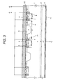
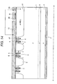
- Fig. 5 shows the fourth embodiment of the present invention and is a plan view of the cell and cell end of the trench insulating gate type IGBT relating to the first embodiment of the present invention.
- Figs. 6 and 7 are cross sectional views of A-A' and B-B' shown in Fig. 5 respectively.
- the p-type well layer 91 is formed at a distance of Lp from the p-type base layer 4 so as to touch - the end of the trench insulating gates 7 and be separated from the p-type base layer 4.
- the distance Lp is preset to a distance which the p-type base layer 4 and the p-type well layer 91 punch through in the voltage inhibition state of the IGBT.
- the p-type well layer 91 is formed at a distance of Lp from the p-type base layer 9 so as to be separated from the p-type well layer 9 in contact with the p-type base layer 4 in the outermost periphery.
- the distance Lp is preset to a distance which the p-type well layer 9 and the p-type well layer 91 punch through in the voltage inhibition state of the IGBT.
- the p-type well layer 91 is electrically connected to the main electrode 10 via the electrode 66. To pull out holes during turn-off, the p-type well layer 9 in the outermost periphery may come in contact with the electrode 10 like the contact 67.
- the p-type base layer 4 positioned in the area Lb can be electrically insulated from the p-type well layer 91 without reducing the main withstand voltage, and holes accumulated in the p-type base layer 4 are not ejected outside the element, and the ON voltage is lowered.
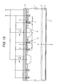
- Fig. 8 is a plan view of the fourth embodiment of the present invention and the basic constitution is the same as that of the first embodiment.
- the cross sectional views of A-A' and B-B' shown in Fig. 8 are those shown in Figs. 6 and 7 respectively.
- the trench insulating gates 7 formed so as to be repeated alternately like the area La and the area Lb are arranged to intersect the trench insulating gates 7 indicated in the second embodiment. 100 to 20000 trench insulating gates in total or so are formed in an actual element.
- the p-type well layer 9 may not be formed in the area Lb.
- the gate wire resistance can be reduced.
- the difference in the delay between a gate signal of the IGBT near to the gate electrode pad or gate input terminal and a gate signal of the IGBT far from it is made smaller, so that the uniformity of the switching operation in the element is improved. Therefore, the element destruction due to current concentration caused by an ununiformoperation can be prevented.
- trench insulating gate electrodes can be structured in the area 101 where the two narrow areas La intersect each other and furthermore, the gate resistance can be reduced.
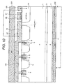
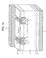
- Fig. 10 shows the sixth embodiment of the present invention and is a cross sectional view of an IGBT chip.
- the basic constitution is the same as that of the first embodiment.
- the plane shape of the trench insulating gates is formed in a mesh-shape as shown in Fig. 8 .
- Numerals 231 and 232 indicate an emitter electrode member and a collector electrode member respectively.
- the emitter electrode member 231 and the collector electrode member 232 are in contact with the main electrodes 10 and 11 by pressure respectively.
- These electrode members in this embodiment, use molybdenum Mo whose coefficient of heat expansion is close to that of a semiconductor layer as a material.
- Numeral 61 indicates gate wires, which are separated from the pressure portion and attached with the conductive metal wires 65 so as to form a resistor.
- the insulating film 161 is formed thicker or higher than the gate wires 61 and the insulating film around them.
- the top of the main electrode 10 is formed higher than the metal wires 65 on the gate wires 61 and the emitter electrode member 231 is not in contact with the metal wires 65 on the gate wires. Since the metal wires 65 for reducing the gate wire resistance are provided, the delay of a gate signal to be transferred to the IGBT can be suppressed. Therefore, the switching delay between the IGBT unit near to the gate pad and the IGBT far from the gate pad is reduced and the current concentration to the IGBT units and heat destruction by it can be prevented.
- the trench insulating gates 7 are arranged so as to intersect each other. As indicated by this embodiment 1, the gate input capacity in this structure can be reduced and also the delay of a gate signal can be suppressed and by pressurizing the main electrodes 10 and 11, the emitter electrode and collector electrode can come into contact with each other.
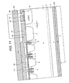
- Fig. 11 shows the seventh embodiment of the present invention and is a cross sectional view of an IGBT chip.
- the basic constitution is the same as that of the sixth embodiment.
- the p-type base layer 4 and the p-type well layer 9 are in contact with the trench insulating gate electrodes so as to be separated by an insulating film and the electrodes 171 connecting the insulating gates are formed in the area Lb.
- the electrodes 171 hold the main electrode 10 high and make the resistance of the gates lower.
- the gate input capacity increases, the difference between the gate input capacity and the feedback capacity does not increase, so that by use of this structure, the delay of a gate signal can be suppressed more. Therefore, by pressurizing the main electrodes 10 and 11, the emitter electrode and collector electrode can come into contact with each other.
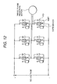
- Fig. 12 shows an example of a power converter using the trench insulating gate type IGBT of the present invention which is a circuit diagram showing an embodiment of a 3-phase invertor for driving an induction motor.
- a diode having a reverse polarity for feeding back the load current is connected in parallel and between the gates and the emitter, a gate driver is connected.
- the two IGBTs connected in series are connected in parallel for three phases respectively.
- Fig. 13 shows the eighth embodiment of the present invention and is a plan view of the cell and cell end of a trench insulating gate type IGBT.
- Fig. 14 is a cross sectional view of A-A' shown in Fig. 13 .
- the basic constitution is the same as that of the fourth embodiment.
- the p-type well layer 9 positioned in the outermost periphery is not provided in the direction of the channel width of the trench insulating gates 7, the p-type base layer 4 and the p-type well layer 91 are overlaid and in contact with each other.
- the p-type base layer 4 and the p-type well layer 91 are in contact with the main electrode 10 like the contact 67.
- Fig. 15 shows the ninth embodiment of the present invention and the basic constitution is the same as that of the first embodiment.
- an M1 source electrode which is a p-type MOS is electrically connected to the p-type well layer 9 and a drain electrode is electrically connected to the main electrode 10.
- An M1 gate electrode is electrically connected to the trench insulating gates 7.
- M1 When the trench insulating gates 7 of the IGBT are turned off by applying a negative potential, M1 may be any one of the enhancement type and the depression type, though when they are turned off by applying a 0 potential, it is necessary to use M1 of the depression type. In either case, when the IGBT is turned on, M1 is turned off and when the IGBT is turned off, M1 is turned on.
- Fig. 16 shows the ninth embodiment of the present invention and is a solid perspective view.
- the p-type well layer 9 is not formed in the area Lb and the p-type base layer 4 is formed continuously.
- the n-type source layer 5 is divided into a plurality of areas. Between neighboring areas, a part of the p-type base layer 4 is positioned. Namely, the n-type source layer 5 is formed intermittently. Almost at the center in the width direction of the area La, a groove which is a contact hole 201 is formed in the longitudinal direction so deep as to pass the n-type source layer 5.
- the area La is divided into two areas by this groove. In these two areas, the n-type source layer 5 is formed respectively in the same way.
- the main electrode 10 (source electrode) is electrically connected to the n-type source layer 5 and the p-type base layer 4 in the same way as with Fig. 1 .
- the main electrode 10 (source electrode) is electrically connected to the n-type source layer 5 and the p-type base layer 4.
- the p+ layer 6 whose impurity density is higher than that of the p-type base layer 4 is formed and the p-type base layer 4 is electrically connected to the main electrode via the p+ layer 6.
- the trench insulating gate type IGBT of this embodiment within the range that the effect of Lb/La on the element withstand voltage is comparatively small, has both low ON voltage and high short-circuit withstand amount.
- the p-type base layer 4 is electrically connected to the main electrode at the bottom of the contact hole 201, so that when the IGBT is turned off, the hole current is ejected to the main electrode 10 without almost passing in the neighborhood of the n-type source layer 5. Therefore, the latch-up phenomenon at the time of turn-off is hardly generated.
- a high performance trench insulating gate type IGBT can be realized.
Landscapes
- Engineering & Computer Science (AREA)
- Microelectronics & Electronic Packaging (AREA)
- Power Engineering (AREA)
- Physics & Mathematics (AREA)
- Ceramic Engineering (AREA)
- Condensed Matter Physics & Semiconductors (AREA)
- General Physics & Mathematics (AREA)
- Computer Hardware Design (AREA)
- Thyristors (AREA)
- Semiconductor Integrated Circuits (AREA)
- Electrodes Of Semiconductors (AREA)
- Metal-Oxide And Bipolar Metal-Oxide Semiconductor Integrated Circuits (AREA)
Applications Claiming Priority (2)
| Application Number | Priority Date | Filing Date | Title |
|---|---|---|---|
| JP3816699 | 1999-02-17 | ||
| EP00301097A EP1032047B9 (fr) | 1999-02-17 | 2000-02-11 | Dispositif semiconducteur et convertisseur de puissance l'utilisant |
Related Parent Applications (2)
| Application Number | Title | Priority Date | Filing Date |
|---|---|---|---|
| EP00301097A Division EP1032047B9 (fr) | 1999-02-17 | 2000-02-11 | Dispositif semiconducteur et convertisseur de puissance l'utilisant |
| EP00301097.2 Division | 2000-02-11 |
Publications (3)
| Publication Number | Publication Date |
|---|---|
| EP2237319A2 true EP2237319A2 (fr) | 2010-10-06 |
| EP2237319A3 EP2237319A3 (fr) | 2010-10-27 |
| EP2237319B1 EP2237319B1 (fr) | 2015-04-08 |
Family
ID=12517825
Family Applications (3)
| Application Number | Title | Priority Date | Filing Date |
|---|---|---|---|
| EP00301097A Expired - Lifetime EP1032047B9 (fr) | 1999-02-17 | 2000-02-11 | Dispositif semiconducteur et convertisseur de puissance l'utilisant |
| EP07009037A Expired - Lifetime EP1811572B1 (fr) | 1999-02-17 | 2000-02-11 | Dispositif à semi-conducteur et convertisseur de puissance utilisant ce même dispositif à semi-conducteur |
| EP10007172.9A Expired - Lifetime EP2237319B1 (fr) | 1999-02-17 | 2000-02-11 | Dispositif semiconducteur et convertisseur de puissance l'utilisant |
Family Applications Before (2)
| Application Number | Title | Priority Date | Filing Date |
|---|---|---|---|
| EP00301097A Expired - Lifetime EP1032047B9 (fr) | 1999-02-17 | 2000-02-11 | Dispositif semiconducteur et convertisseur de puissance l'utilisant |
| EP07009037A Expired - Lifetime EP1811572B1 (fr) | 1999-02-17 | 2000-02-11 | Dispositif à semi-conducteur et convertisseur de puissance utilisant ce même dispositif à semi-conducteur |
Country Status (3)
| Country | Link |
|---|---|
| EP (3) | EP1032047B9 (fr) |
| KR (1) | KR100745557B1 (fr) |
| DE (1) | DE60044992D1 (fr) |
Cited By (3)
| Publication number | Priority date | Publication date | Assignee | Title |
|---|---|---|---|---|
| DE102017104716B4 (de) | 2016-03-09 | 2020-06-18 | Denso Corporation | Schaltvorrichtung |
| DE102017104715B4 (de) | 2016-03-09 | 2022-09-08 | Toyota Jidosha Kabushiki Kaisha | Schaltvorrichtung |
| DE102017104713B4 (de) | 2016-03-09 | 2022-12-15 | Denso Corporation | Schaltvorrichtung |
Families Citing this family (31)
| Publication number | Priority date | Publication date | Assignee | Title |
|---|---|---|---|---|
| JP2001168333A (ja) * | 1999-09-30 | 2001-06-22 | Toshiba Corp | トレンチゲート付き半導体装置 |
| EP1451921A4 (fr) * | 2001-11-02 | 2006-01-11 | Aker Wade Power Technologies L | Chargeur rapide pour batteries haute capacite |
| US7301308B2 (en) | 2001-11-02 | 2007-11-27 | Aker Wade Power Technologies, Llc | Fast charger for high capacity batteries |
| JP4085781B2 (ja) * | 2002-11-01 | 2008-05-14 | トヨタ自動車株式会社 | 電界効果型半導体装置 |
| JP4136778B2 (ja) * | 2003-05-07 | 2008-08-20 | 富士電機デバイステクノロジー株式会社 | 絶縁ゲート型バイポーラトランジスタ |
| JP4799829B2 (ja) * | 2003-08-27 | 2011-10-26 | 三菱電機株式会社 | 絶縁ゲート型トランジスタ及びインバータ回路 |
| JP4703138B2 (ja) | 2004-06-18 | 2011-06-15 | 株式会社東芝 | 絶縁ゲート型半導体装置 |
| JP4731848B2 (ja) * | 2004-07-16 | 2011-07-27 | 株式会社豊田中央研究所 | 半導体装置 |
| JP5017850B2 (ja) * | 2005-11-30 | 2012-09-05 | 株式会社日立製作所 | 電力用半導体装置およびそれを用いた電力変換装置 |
| JP5044950B2 (ja) | 2006-03-14 | 2012-10-10 | 株式会社デンソー | 半導体装置 |
| EP2003694B1 (fr) * | 2007-06-14 | 2011-11-23 | Denso Corporation | Dispositif semi-conducteur |
| JP5561922B2 (ja) | 2008-05-20 | 2014-07-30 | 三菱電機株式会社 | パワー半導体装置 |
| JP4644730B2 (ja) * | 2008-08-12 | 2011-03-02 | 株式会社日立製作所 | 半導体装置及びそれを用いた電力変換装置 |
| US8344480B2 (en) | 2008-09-30 | 2013-01-01 | Ixys Corporation | Insulated gate bipolar transistor |
| JP5423018B2 (ja) * | 2009-02-02 | 2014-02-19 | 三菱電機株式会社 | 半導体装置 |
| EP2523217A4 (fr) * | 2010-01-04 | 2014-06-25 | Hitachi Ltd | Dispositif semi-conducteur et dispositif de conversion de puissance électrique l'utilisant |
| KR101840903B1 (ko) * | 2011-07-07 | 2018-03-21 | 에이비비 슈바이쯔 아게 | 절연 게이트 바이폴라 트랜지스터 |
| WO2013007654A1 (fr) * | 2011-07-14 | 2013-01-17 | Abb Technology Ag | Transistor bipolaire à grille isolee |
| JP5720805B2 (ja) * | 2011-11-28 | 2015-05-20 | 富士電機株式会社 | 絶縁ゲート型半導体装置およびその製造方法 |
| JP5973730B2 (ja) | 2012-01-05 | 2016-08-23 | ルネサスエレクトロニクス株式会社 | Ie型トレンチゲートigbt |
| KR101311538B1 (ko) * | 2012-01-19 | 2013-09-25 | 주식회사 케이이씨 | 전력 반도체 디바이스 및 그 제조 방법 |
| JP6072445B2 (ja) | 2012-06-28 | 2017-02-01 | 株式会社 日立パワーデバイス | 半導体装置およびそれを用いた電力変換装置 |
| US9595602B2 (en) | 2012-09-07 | 2017-03-14 | Hitachi, Ltd. | Switching device for power conversion and power conversion device |
| US20170309704A1 (en) * | 2015-01-14 | 2017-10-26 | Mitsubishi Electric Corporation | Semiconductor device and manufacturing method therefor |
| JP6804379B2 (ja) * | 2017-04-24 | 2020-12-23 | 三菱電機株式会社 | 半導体装置 |
| CN107464839B (zh) * | 2017-08-17 | 2020-02-04 | 电子科技大学 | 一种防止关断失效的栅控晶闸管器件 |
| CN108493242B (zh) * | 2018-05-31 | 2020-08-28 | 电子科技大学 | 一种优化体内电场的载流子增强型igbt器件 |
| CN108767006B (zh) * | 2018-05-31 | 2020-09-15 | 电子科技大学 | 一种集成电压采样功能的igbt器件 |
| CN111384149B (zh) * | 2018-12-29 | 2021-05-14 | 比亚迪半导体股份有限公司 | 沟槽型igbt及其制备方法 |
| CN110416294B (zh) * | 2019-08-29 | 2021-01-08 | 电子科技大学 | 一种高耐压低损耗超结功率器件 |
| CN113793807B (zh) * | 2021-11-18 | 2022-02-11 | 南京华瑞微集成电路有限公司 | 一种集成源漏电容的超结mos器件及其制作方法 |
Citations (2)
| Publication number | Priority date | Publication date | Assignee | Title |
|---|---|---|---|---|
| JPH05243561A (ja) | 1991-08-08 | 1993-09-21 | Toshiba Corp | 電力用半導体素子 |
| JPH10178176A (ja) | 1996-12-06 | 1998-06-30 | Semikron Elektron Gmbh | トレンチ・ゲート構造を有するトレンチ・ゲート形絶縁ゲート・バイポーラ・トランジスタ |
Family Cites Families (11)
| Publication number | Priority date | Publication date | Assignee | Title |
|---|---|---|---|---|
| US4712124A (en) * | 1986-12-22 | 1987-12-08 | North American Philips Corporation | Complementary lateral insulated gate rectifiers with matched "on" resistances |
| DE4407279C1 (de) * | 1994-03-04 | 1994-10-13 | Siemens Ag | Halbleiterbauelement für den Überspannungsschutz von MOSFET und IGBT |
| DE69432407D1 (de) * | 1994-05-19 | 2003-05-08 | Cons Ric Microelettronica | Integrierte Leistungsschaltung ("PIC") mit vertikalem IGB und Verfahren zur Herstellung derselben |
| JPH08116056A (ja) * | 1994-10-19 | 1996-05-07 | Hitachi Ltd | 電圧駆動型半導体装置及びそれを用いた電力変換装置 |
| DE69617098T2 (de) | 1995-06-02 | 2002-04-18 | Siliconix Inc | Grabengate-Leistungs-MOSFET mit Schutzdioden in periodischer Anordnung |
| KR100187635B1 (ko) * | 1996-03-20 | 1999-07-01 | 김충환 | 단락 애노우드 수평형 절연 게이트 바이폴라 트랜지스터 |
| JP2776365B2 (ja) * | 1996-04-04 | 1998-07-16 | 日本電気株式会社 | 多段接続型半導体用キャリヤーとそれを用いた半導体装置、及びその製造方法 |
| KR100200366B1 (ko) * | 1996-10-31 | 1999-06-15 | 윤종용 | 절연 게이트 바이폴라 트랜지스터 |
| JPH118385A (ja) * | 1997-06-18 | 1999-01-12 | Hitachi Ltd | 内燃機関用点火装置およびigbt |
| US6110799A (en) * | 1997-06-30 | 2000-08-29 | Intersil Corporation | Trench contact process |
| DE19727676A1 (de) * | 1997-06-30 | 1999-01-07 | Asea Brown Boveri | MOS gesteuertes Leistungshalbleiterbauelement |
-
2000
- 2000-02-09 KR KR1020000005888A patent/KR100745557B1/ko active IP Right Grant
- 2000-02-11 EP EP00301097A patent/EP1032047B9/fr not_active Expired - Lifetime
- 2000-02-11 DE DE60044992T patent/DE60044992D1/de not_active Expired - Lifetime
- 2000-02-11 EP EP07009037A patent/EP1811572B1/fr not_active Expired - Lifetime
- 2000-02-11 EP EP10007172.9A patent/EP2237319B1/fr not_active Expired - Lifetime
Patent Citations (2)
| Publication number | Priority date | Publication date | Assignee | Title |
|---|---|---|---|---|
| JPH05243561A (ja) | 1991-08-08 | 1993-09-21 | Toshiba Corp | 電力用半導体素子 |
| JPH10178176A (ja) | 1996-12-06 | 1998-06-30 | Semikron Elektron Gmbh | トレンチ・ゲート構造を有するトレンチ・ゲート形絶縁ゲート・バイポーラ・トランジスタ |
Cited By (3)
| Publication number | Priority date | Publication date | Assignee | Title |
|---|---|---|---|---|
| DE102017104716B4 (de) | 2016-03-09 | 2020-06-18 | Denso Corporation | Schaltvorrichtung |
| DE102017104715B4 (de) | 2016-03-09 | 2022-09-08 | Toyota Jidosha Kabushiki Kaisha | Schaltvorrichtung |
| DE102017104713B4 (de) | 2016-03-09 | 2022-12-15 | Denso Corporation | Schaltvorrichtung |
Also Published As
| Publication number | Publication date |
|---|---|
| EP1032047A2 (fr) | 2000-08-30 |
| DE60044992D1 (de) | 2010-11-04 |
| EP1032047A3 (fr) | 2001-11-28 |
| EP1811572A3 (fr) | 2007-09-19 |
| KR20000076628A (ko) | 2000-12-26 |
| EP2237319B1 (fr) | 2015-04-08 |
| EP1811572A2 (fr) | 2007-07-25 |
| EP1811572B1 (fr) | 2012-05-30 |
| EP2237319A3 (fr) | 2010-10-27 |
| EP1032047B9 (fr) | 2011-02-09 |
| KR100745557B1 (ko) | 2007-08-02 |
| EP1032047B1 (fr) | 2010-09-22 |
Similar Documents
| Publication | Publication Date | Title |
|---|---|---|
| EP1032047B9 (fr) | Dispositif semiconducteur et convertisseur de puissance l'utilisant | |
| JP4310017B2 (ja) | 半導体装置及び電力変換装置 | |
| US6580108B1 (en) | Insulated gate bipolar transistor decreasing the gate resistance | |
| US8193578B2 (en) | Power supply circuit having a semiconductor device including a MOSFET and a Schottky junction | |
| US8102025B2 (en) | Semiconductor device having IGBT and diode | |
| JP5452195B2 (ja) | 半導体装置及びそれを用いた電力変換装置 | |
| US6133607A (en) | Semiconductor device | |
| EP0526037A1 (fr) | Transistor bipolaire latéral à grille isolée | |
| KR0160953B1 (ko) | 횡형 절연 게이트 바이폴라 트랜지스터 | |
| JP4829003B2 (ja) | 半導体装置及び電力変換装置 | |
| EP0565350B1 (fr) | Dispositif à semiconducteur avec une couche tampon | |
| JP3257394B2 (ja) | 電圧駆動型半導体装置 | |
| US6864535B2 (en) | Controllable semiconductor switching element that blocks in both directions | |
| KR20220016134A (ko) | 파워 트랜지스터 셀 및 파워 트랜지스터 | |
| CN116314276B (zh) | 半导体器件 | |
| CN116247055B (zh) | 半导体器件 | |
| KR102030466B1 (ko) | 레터럴 타입의 전력 반도체 소자 | |
| CN118073422A (en) | High-resistance SiC VDMOSFET device and preparation method thereof | |
| JPH1140818A (ja) | 半導体装置 | |
| JPH11214690A (ja) | 半導体素子および平型半導体装置 |
Legal Events
| Date | Code | Title | Description |
|---|---|---|---|
| PUAI | Public reference made under article 153(3) epc to a published international application that has entered the european phase |
Free format text: ORIGINAL CODE: 0009012 |
|
| PUAL | Search report despatched |
Free format text: ORIGINAL CODE: 0009013 |
|
| 17P | Request for examination filed |
Effective date: 20100728 |
|
| AC | Divisional application: reference to earlier application |
Ref document number: 1032047 Country of ref document: EP Kind code of ref document: P |
|
| AK | Designated contracting states |
Kind code of ref document: A2 Designated state(s): DE FR GB |
|
| AK | Designated contracting states |
Kind code of ref document: A3 Designated state(s): DE FR GB |
|
| RIN1 | Information on inventor provided before grant (corrected) |
Inventor name: MORI, MUTSUHIRO Inventor name: SAKANO, JYUNICHI Inventor name: OYAMA, KAZUHIRO |
|
| 17Q | First examination report despatched |
Effective date: 20120227 |
|
| GRAP | Despatch of communication of intention to grant a patent |
Free format text: ORIGINAL CODE: EPIDOSNIGR1 |
|
| RAP1 | Party data changed (applicant data changed or rights of an application transferred) |
Owner name: HITACHI POWER SEMICONDUCTOR DEVICE, LTD. |
|
| INTG | Intention to grant announced |
Effective date: 20140917 |
|
| GRAS | Grant fee paid |
Free format text: ORIGINAL CODE: EPIDOSNIGR3 |
|
| GRAA | (expected) grant |
Free format text: ORIGINAL CODE: 0009210 |
|
| AC | Divisional application: reference to earlier application |
Ref document number: 1032047 Country of ref document: EP Kind code of ref document: P |
|
| AK | Designated contracting states |
Kind code of ref document: B1 Designated state(s): DE FR GB |
|
| REG | Reference to a national code |
Ref country code: GB Ref legal event code: FG4D |
|
| REG | Reference to a national code |
Ref country code: DE Ref legal event code: R096 Ref document number: 60048924 Country of ref document: DE Effective date: 20150521 |
|
| REG | Reference to a national code |
Ref country code: DE Ref legal event code: R097 Ref document number: 60048924 Country of ref document: DE |
|
| PLBE | No opposition filed within time limit |
Free format text: ORIGINAL CODE: 0009261 |
|
| STAA | Information on the status of an ep patent application or granted ep patent |
Free format text: STATUS: NO OPPOSITION FILED WITHIN TIME LIMIT |
|
| REG | Reference to a national code |
Ref country code: FR Ref legal event code: PLFP Year of fee payment: 17 |
|
| 26N | No opposition filed |
Effective date: 20160111 |
|
| REG | Reference to a national code |
Ref country code: FR Ref legal event code: PLFP Year of fee payment: 18 |
|
| REG | Reference to a national code |
Ref country code: FR Ref legal event code: PLFP Year of fee payment: 19 |
|
| PGFP | Annual fee paid to national office [announced via postgrant information from national office to epo] |
Ref country code: DE Payment date: 20190129 Year of fee payment: 20 Ref country code: GB Payment date: 20190206 Year of fee payment: 20 Ref country code: FR Payment date: 20190111 Year of fee payment: 20 |
|
| REG | Reference to a national code |
Ref country code: DE Ref legal event code: R082 Ref document number: 60048924 Country of ref document: DE Representative=s name: MEWBURN ELLIS LLP, DE |
|
| REG | Reference to a national code |
Ref country code: DE Ref legal event code: R071 Ref document number: 60048924 Country of ref document: DE |
|
| REG | Reference to a national code |
Ref country code: GB Ref legal event code: PE20 Expiry date: 20200210 |
|
| PG25 | Lapsed in a contracting state [announced via postgrant information from national office to epo] |
Ref country code: GB Free format text: LAPSE BECAUSE OF EXPIRATION OF PROTECTION Effective date: 20200210 |