EP2175493B1 - Field effect transistor and process for production thereof - Google Patents
Field effect transistor and process for production thereof Download PDFInfo
- Publication number
- EP2175493B1 EP2175493B1 EP09012657A EP09012657A EP2175493B1 EP 2175493 B1 EP2175493 B1 EP 2175493B1 EP 09012657 A EP09012657 A EP 09012657A EP 09012657 A EP09012657 A EP 09012657A EP 2175493 B1 EP2175493 B1 EP 2175493B1
- Authority
- EP
- European Patent Office
- Prior art keywords
- oxynitride
- film
- nitrogen
- electrode
- oxide semiconductor
- Prior art date
- Legal status (The legal status is an assumption and is not a legal conclusion. Google has not performed a legal analysis and makes no representation as to the accuracy of the status listed.)
- Not-in-force
Links
- 238000000034 method Methods 0.000 title claims description 35
- 230000005669 field effect Effects 0.000 title claims description 29
- 230000008569 process Effects 0.000 title claims description 23
- 238000004519 manufacturing process Methods 0.000 title description 4
- IJGRMHOSHXDMSA-UHFFFAOYSA-N Atomic nitrogen Chemical compound N#N IJGRMHOSHXDMSA-UHFFFAOYSA-N 0.000 claims description 70
- 239000004065 semiconductor Substances 0.000 claims description 52
- 229910052757 nitrogen Inorganic materials 0.000 claims description 45
- 239000000758 substrate Substances 0.000 claims description 35
- 230000003287 optical effect Effects 0.000 claims description 24
- 238000004544 sputter deposition Methods 0.000 claims description 24
- 229910052751 metal Inorganic materials 0.000 claims description 23
- 239000012298 atmosphere Substances 0.000 claims description 11
- QVGXLLKOCUKJST-UHFFFAOYSA-N atomic oxygen Chemical compound [O] QVGXLLKOCUKJST-UHFFFAOYSA-N 0.000 claims description 9
- 229910052760 oxygen Inorganic materials 0.000 claims description 9
- 239000001301 oxygen Substances 0.000 claims description 9
- 229910052738 indium Inorganic materials 0.000 claims description 6
- 125000004433 nitrogen atom Chemical group N* 0.000 claims description 5
- APFVFJFRJDLVQX-UHFFFAOYSA-N indium atom Chemical compound [In] APFVFJFRJDLVQX-UHFFFAOYSA-N 0.000 claims description 4
- 125000004430 oxygen atom Chemical group O* 0.000 claims description 3
- 239000013078 crystal Substances 0.000 claims description 2
- 150000004767 nitrides Chemical class 0.000 claims description 2
- JBQYATWDVHIOAR-UHFFFAOYSA-N tellanylidenegermanium Chemical group [Te]=[Ge] JBQYATWDVHIOAR-UHFFFAOYSA-N 0.000 claims 3
- 238000005477 sputtering target Methods 0.000 claims 1
- 239000010408 film Substances 0.000 description 111
- 239000010409 thin film Substances 0.000 description 58
- XLOMVQKBTHCTTD-UHFFFAOYSA-N Zinc monoxide Chemical compound [Zn]=O XLOMVQKBTHCTTD-UHFFFAOYSA-N 0.000 description 34
- 230000015572 biosynthetic process Effects 0.000 description 30
- 239000000463 material Substances 0.000 description 17
- 239000011787 zinc oxide Substances 0.000 description 17
- 239000007789 gas Substances 0.000 description 14
- 229910007611 Zn—In—O Inorganic materials 0.000 description 13
- 239000002184 metal Substances 0.000 description 13
- 239000011701 zinc Substances 0.000 description 13
- -1 InGaZnO4 Substances 0.000 description 11
- 238000011156 evaluation Methods 0.000 description 10
- VYPSYNLAJGMNEJ-UHFFFAOYSA-N Silicium dioxide Chemical compound O=[Si]=O VYPSYNLAJGMNEJ-UHFFFAOYSA-N 0.000 description 9
- 238000002441 X-ray diffraction Methods 0.000 description 8
- 229910007541 Zn O Inorganic materials 0.000 description 8
- 239000011521 glass Substances 0.000 description 8
- PJXISJQVUVHSOJ-UHFFFAOYSA-N indium(III) oxide Inorganic materials [O-2].[O-2].[O-2].[In+3].[In+3] PJXISJQVUVHSOJ-UHFFFAOYSA-N 0.000 description 8
- 230000035515 penetration Effects 0.000 description 8
- 150000002500 ions Chemical class 0.000 description 6
- 230000031700 light absorption Effects 0.000 description 6
- 239000000203 mixture Substances 0.000 description 6
- 239000010931 gold Substances 0.000 description 5
- 238000005468 ion implantation Methods 0.000 description 5
- 229910052814 silicon oxide Inorganic materials 0.000 description 5
- XKRFYHLGVUSROY-UHFFFAOYSA-N Argon Chemical compound [Ar] XKRFYHLGVUSROY-UHFFFAOYSA-N 0.000 description 4
- 238000010438 heat treatment Methods 0.000 description 4
- 229910052725 zinc Inorganic materials 0.000 description 4
- VVTSZOCINPYFDP-UHFFFAOYSA-N [O].[Ar] Chemical compound [O].[Ar] VVTSZOCINPYFDP-UHFFFAOYSA-N 0.000 description 3
- 238000009792 diffusion process Methods 0.000 description 3
- 229910052737 gold Inorganic materials 0.000 description 3
- 230000003071 parasitic effect Effects 0.000 description 3
- 239000004033 plastic Substances 0.000 description 3
- UFHFLCQGNIYNRP-UHFFFAOYSA-N Hydrogen Chemical compound [H][H] UFHFLCQGNIYNRP-UHFFFAOYSA-N 0.000 description 2
- 238000004833 X-ray photoelectron spectroscopy Methods 0.000 description 2
- 238000010521 absorption reaction Methods 0.000 description 2
- 229910021417 amorphous silicon Inorganic materials 0.000 description 2
- 238000000137 annealing Methods 0.000 description 2
- 229910052786 argon Inorganic materials 0.000 description 2
- 230000008859 change Effects 0.000 description 2
- 229910052681 coesite Inorganic materials 0.000 description 2
- 150000001875 compounds Chemical class 0.000 description 2
- 229910052906 cristobalite Inorganic materials 0.000 description 2
- 230000003247 decreasing effect Effects 0.000 description 2
- 230000006866 deterioration Effects 0.000 description 2
- 229910001873 dinitrogen Inorganic materials 0.000 description 2
- 229910001882 dioxygen Inorganic materials 0.000 description 2
- PCHJSUWPFVWCPO-UHFFFAOYSA-N gold Chemical compound [Au] PCHJSUWPFVWCPO-UHFFFAOYSA-N 0.000 description 2
- 239000001257 hydrogen Substances 0.000 description 2
- 229910052739 hydrogen Inorganic materials 0.000 description 2
- 239000004973 liquid crystal related substance Substances 0.000 description 2
- QJGQUHMNIGDVPM-UHFFFAOYSA-N nitrogen group Chemical group [N] QJGQUHMNIGDVPM-UHFFFAOYSA-N 0.000 description 2
- 229910021420 polycrystalline silicon Inorganic materials 0.000 description 2
- 238000005001 rutherford backscattering spectroscopy Methods 0.000 description 2
- 238000001004 secondary ion mass spectrometry Methods 0.000 description 2
- 239000000377 silicon dioxide Substances 0.000 description 2
- 239000007787 solid Substances 0.000 description 2
- 239000011343 solid material Substances 0.000 description 2
- 229910052682 stishovite Inorganic materials 0.000 description 2
- 238000012546 transfer Methods 0.000 description 2
- 229910052905 tridymite Inorganic materials 0.000 description 2
- 238000007740 vapor deposition Methods 0.000 description 2
- UFHFLCQGNIYNRP-VVKOMZTBSA-N Dideuterium Chemical compound [2H][2H] UFHFLCQGNIYNRP-VVKOMZTBSA-N 0.000 description 1
- 229910002601 GaN Inorganic materials 0.000 description 1
- 229910052774 Proactinium Inorganic materials 0.000 description 1
- ATJFFYVFTNAWJD-UHFFFAOYSA-N Tin Chemical compound [Sn] ATJFFYVFTNAWJD-UHFFFAOYSA-N 0.000 description 1
- HCHKCACWOHOZIP-UHFFFAOYSA-N Zinc Chemical compound [Zn] HCHKCACWOHOZIP-UHFFFAOYSA-N 0.000 description 1
- 229910007604 Zn—Sn—O Inorganic materials 0.000 description 1
- 230000001133 acceleration Effects 0.000 description 1
- 230000002411 adverse Effects 0.000 description 1
- 229910052782 aluminium Inorganic materials 0.000 description 1
- PNEYBMLMFCGWSK-UHFFFAOYSA-N aluminium oxide Inorganic materials [O-2].[O-2].[O-2].[Al+3].[Al+3] PNEYBMLMFCGWSK-UHFFFAOYSA-N 0.000 description 1
- 238000004458 analytical method Methods 0.000 description 1
- 238000004320 controlled atmosphere Methods 0.000 description 1
- 229910052593 corundum Inorganic materials 0.000 description 1
- 238000000151 deposition Methods 0.000 description 1
- 230000008021 deposition Effects 0.000 description 1
- 238000013461 design Methods 0.000 description 1
- 238000011161 development Methods 0.000 description 1
- 230000018109 developmental process Effects 0.000 description 1
- 230000005685 electric field effect Effects 0.000 description 1
- 239000012789 electroconductive film Substances 0.000 description 1
- 238000010894 electron beam technology Methods 0.000 description 1
- 230000007613 environmental effect Effects 0.000 description 1
- 238000001704 evaporation Methods 0.000 description 1
- 229910052733 gallium Inorganic materials 0.000 description 1
- CJNBYAVZURUTKZ-UHFFFAOYSA-N hafnium(IV) oxide Inorganic materials O=[Hf]=O CJNBYAVZURUTKZ-UHFFFAOYSA-N 0.000 description 1
- 239000012535 impurity Substances 0.000 description 1
- 229910003437 indium oxide Inorganic materials 0.000 description 1
- 238000009413 insulation Methods 0.000 description 1
- 238000012986 modification Methods 0.000 description 1
- 230000004048 modification Effects 0.000 description 1
- 229910052759 nickel Inorganic materials 0.000 description 1
- 239000012299 nitrogen atmosphere Substances 0.000 description 1
- 229910000510 noble metal Inorganic materials 0.000 description 1
- 239000002245 particle Substances 0.000 description 1
- 238000000206 photolithography Methods 0.000 description 1
- 239000002985 plastic film Substances 0.000 description 1
- 229920006255 plastic film Polymers 0.000 description 1
- 229910052697 platinum Inorganic materials 0.000 description 1
- 229920000307 polymer substrate Polymers 0.000 description 1
- 229920005591 polysilicon Polymers 0.000 description 1
- 230000004044 response Effects 0.000 description 1
- 230000000630 rising effect Effects 0.000 description 1
- 238000004611 spectroscopical analysis Methods 0.000 description 1
- 238000010408 sweeping Methods 0.000 description 1
- 230000007704 transition Effects 0.000 description 1
- 238000000411 transmission spectrum Methods 0.000 description 1
- 229910052721 tungsten Inorganic materials 0.000 description 1
- 238000001771 vacuum deposition Methods 0.000 description 1
- 238000004876 x-ray fluorescence Methods 0.000 description 1
- 229910001845 yogo sapphire Inorganic materials 0.000 description 1
- RUDFQVOCFDJEEF-UHFFFAOYSA-N yttrium(III) oxide Inorganic materials [O-2].[O-2].[O-2].[Y+3].[Y+3] RUDFQVOCFDJEEF-UHFFFAOYSA-N 0.000 description 1
- 229910052984 zinc sulfide Inorganic materials 0.000 description 1
Images


Classifications
-
- H—ELECTRICITY
- H10—SEMICONDUCTOR DEVICES; ELECTRIC SOLID-STATE DEVICES NOT OTHERWISE PROVIDED FOR
- H10D—INORGANIC ELECTRIC SEMICONDUCTOR DEVICES
- H10D30/00—Field-effect transistors [FET]
- H10D30/60—Insulated-gate field-effect transistors [IGFET]
- H10D30/67—Thin-film transistors [TFT]
- H10D30/674—Thin-film transistors [TFT] characterised by the active materials
- H10D30/6755—Oxide semiconductors, e.g. zinc oxide, copper aluminium oxide or cadmium stannate
-
- H—ELECTRICITY
- H10—SEMICONDUCTOR DEVICES; ELECTRIC SOLID-STATE DEVICES NOT OTHERWISE PROVIDED FOR
- H10D—INORGANIC ELECTRIC SEMICONDUCTOR DEVICES
- H10D30/00—Field-effect transistors [FET]
- H10D30/60—Insulated-gate field-effect transistors [IGFET]
- H10D30/67—Thin-film transistors [TFT]
- H10D30/6704—Thin-film transistors [TFT] having supplementary regions or layers in the thin films or in the insulated bulk substrates for controlling properties of the device
- H10D30/6713—Thin-film transistors [TFT] having supplementary regions or layers in the thin films or in the insulated bulk substrates for controlling properties of the device characterised by the properties of the source or drain regions, e.g. compositions or sectional shapes
-
- H—ELECTRICITY
- H10—SEMICONDUCTOR DEVICES; ELECTRIC SOLID-STATE DEVICES NOT OTHERWISE PROVIDED FOR
- H10D—INORGANIC ELECTRIC SEMICONDUCTOR DEVICES
- H10D64/00—Electrodes of devices having potential barriers
- H10D64/60—Electrodes characterised by their materials
- H10D64/62—Electrodes ohmically coupled to a semiconductor
Definitions
- the present invention relates to a field effect transistor employing a semiconductor film composed of an oxide as the channel.
- the present invention relates also to a process for producing the transistor.
- the field effect transistor is a three-terminal element comprising a gate electrode, a source electrode, and a drain electrode.
- This FET is an electron-active element for controlling and switching, by application of a voltage to a gate electrode, the current flowing through the channel layer between the source electrode and the drain electrode.
- the FET employing a semiconductor thin film as a channel layer is called a thin film transistor (TFT).
- the TFT based on the thin film technique, can readily be formed in a large area on a substrate advantageously. Therefore, the TFTs are widely used as a driving element of a flat panel display like a liquid crystal display.
- the pixels are turned on and off by TFT formed on a glass substrate.
- OLED organic light-emitting diode display
- the TFTs employing a polycrystalline silicon film or an amorphous silicon film are widely used as the material for the channel layer at the moment.
- the amorphous silicon TFT or the polysilicon TFT is necessarily processed at a high temperature in the device production, which makes difficult the formation of the thin film on a substrate like a plastic substrate or a film.
- semiconductor materials composed mainly of an oxide are attracting attention as the material for the TFT to be formed on a polymer substrate, a film, or a glass substrate.
- TFTs are developed actively which employ a transparent oxide thin film constituted mainly of ZnO (zinc oxide).
- a thin film transistor is disclosed which employs an In-Ga-Zn-O type of amorphous oxide.
- Such TFTs are described in documents, for example: U.S. Patent Application Publication No. 2007/0194379 (corresponding to International Publication No. 2005/088726 ), US 2007/108446 A1 , US 2006/108636A1 , WO 2008/133345 A , EP 1 770 788A , and Nature, vol. 432, pp. 488-492, (2004 ).
- Such a transistor can be formed at a room temperature on a plastic or glass substrate, and has a transistor characteristic of normally-off type at an electric field effect mobility of about 6-9 cm 2 (Vs) -1 .
- the resistance between the semiconductor and the source electrode or the drain electrode is preferably lower, and the electric connection is preferably stabler in the environment or in the driving.
- electrodes of the amorphous oxide thin film transistor employ oxide electrodes such as ITO (In 2 O 3 :Sn, tin-containing indium oxide), and metal electrodes such as Au (gold) ( Thin Solid Films, 516 (2008) 5899 ).
- a noble metal such as gold does not have sufficient adhesiveness to an oxide semiconductor, and is less reliable in that the metal electrode produced by a productive process like vacuum deposition or sputtering is easy to be peeled off.
- an electrode composed of an oxide like In 2 O 3 :Sn (ITO) is preferred for the adhesiveness.
- ITO In 2 O 3 :Sn
- the surface property of such an oxide electrode can be affected in the film forming process or the post-treatment including a heat treatment and a solution treatment to cause variation in electric connection with the semiconductor.
- An object of the present invention is to provide an electrode which enables stable electric connection to the oxide semiconductor with a lower contact resistance.
- amorphous InGaZnO 4 has an optical band gap of about 2.9 eV, being transparent to visible light.
- a transistor employing the amorphous InGaZnO 4 as the channel can change its characteristic on exposure to near-ultraviolet light having a wavelength of shorter than about 450 nm (higher than about 2.7 eV).
- the transistor using such a material vary their characteristics. Display device using the transistor tends to cause deterioration of the image quality on irradiation of a display light or an external light onto the TFT.
- a light-shielding layer may be placed on or under the TFT to intercept the light. This will limit the layout of the TFT and increase the production steps. Further, even with the light-shielding layer, depending on the constitution, a trace amount of stray light can irradiate the TFT, unexpectedly.
- the stray light herein signifies the light introduced to the TFT from an unspecified portion by reflection or refraction by inside or outside of the element. Therefore, the TFT insensive to the light is desired.
- a second object of the present invention is to provide a thin film transistor which has characteristics less affected by irradiation of stray light.
- the field effect transistor of the present invention employs an oxide semiconductor as the channel layer, and an oxynitride as the source electrode and/or the drain electrode, which stabilizes the electric connection between the channel region and the source electrode and/or drain electrode and improves the uniformity and reliability of the elements.
- the electrode constituted of an oxynitride absorbs near-ultraviolet light to prevent penetration of the near-ultraviolet light through the source electrode portion or the drain electrode portion.
- the constitution of the present invention prevents variation of the TFT characteristics even when stray light is generated within the TFT substrate (substrate on which an array of TFTs is formed) and provides a TFT substrate which has stable characteristics against irradiation of near-ultraviolet light.
- FIGS. 1A and 1B are sectional views of a constitution of the thin film transistor of the present invention.
- FIG. 1A illustrates a top-gate structure.
- FIG. 1B illustrates a bottom-gate structure.
- FIG. 2 is a sectional view of a thin film transistor of a coplanar structure of the present invention.
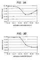
- FIGS. 3A and 3B are graphs of dependence of the resistivity on a nitrogen concentration of a nitrogen-ion-containing oxide film: FIG. 3A , of an In-Ga-Zn-O type; FIG. 3B , of a Zn-In-O type.
- FIG. 4 is a graph of dependence of the optical band gap on the compositional ratio of N/ (N+O) of an oxynitride thin film of a Zn-In-O-N type.
- FIGS. 5A and 5B are graphs showing transistor characteristics of a thin film transistor of the present invention: FIG. 5A showing the transistor characteristics (Id-Vd characteristics); and FIG. 5B showing the transfer characteristics (Id-Vg characteristics).
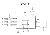
- FIG. 6 illustrates schematically a sputtering apparatus for production of an oxynitride thin film.
- FIGS. 7A, 7B, and 7C illustrate a process for producing a coplanar type thin film transistor of the present invention.
- FIGS. 1A and 1B , and FIG. 2 are sectional views illustrating respectively a constitution of the field effect transistor of the present invention.
- the reference numerals denote the following members: 10, a substrate; 11, a channel layer (oxide semiconductor); 12, a gate-insulating layer (or a gate-insulating film); 13, a source electrode; 14, a drain electrode, and 15, a gate electrode.
- FIG. 1A illustrates a top-gate structure having gate-insulating layer 12, and gate electrode 15 formed in this order on channel layer 11.
- FIG. 1B illustrates a bottom-gate structure having gate-insulating layer 12 and semiconductor channel layer 11 formed in this order on gate electrode 15.
- FIG. 2 illustrates a coplanar structure having channel region 18, source region 16, and drain region 17 placed on the same plane.
- the present invention is applicable to any of the TFT constitutions including the top-gate structures (normal stagger structures), the bottom-gate structures (inverted stagger structures), and the coplanar structures.
- the field effect transistor (FET) employing an oxide semiconductor as the channel of the present invention is characterized by the source electrode 13 and/or drain electrode 14 constituted of a material (oxynitride) containing a metallic element or elements, oxygen, and nitrogen.
- oxynitride a material containing a metallic element or elements, oxygen, and nitrogen.
- the inventors of the present invention have found that the electro-conductive film composed of the oxynitride is connectable well electrically to an oxide semiconductor (like InGaZnO4, ZnO, etc.) with high reliability.
- compositional ratio of oxygen and nitrogen in the oxynitride, (nitrogen atoms)/(nitrogen atoms plus oxygen atoms) is not less than 0.01 as mentioned later.
- the concentration of nitrogen, oxygen, and the metal in the oxynitride film can be determined by SIMS (secondary ion mass spectrometry), RBS (Rutherford backscattering spectroscopy), XPS (X-ray photoelectron spectroscopy), XRF (X-ray fluorescence analysis), and a like method.
- SIMS secondary ion mass spectrometry
- RBS Rutherford backscattering spectroscopy
- XPS X-ray photoelectron spectroscopy
- XRF X-ray fluorescence analysis
- the metallic element for constituting the oxynitride of the electrode includes Zn (zinc), and In (indium) .
- the oxynitride includes types of In-O-N, Zn-In-O-N, Zn-Ga-O-N, Zn-Ge-O-N, Zn-In-Ga-O-N, In-Sn-O-N, Zn-Sn-O-N, and so forth. Of these, the materials containing Zn as the main metallic element are preferred for obtaining the lower resistivity.
- Zn-In-O-N type oxynitride films are preferred for achieving a resistivity, for example, ranging from 1 m ⁇ cm (1 ⁇ 10 -3 ⁇ cm) to 10 m ⁇ cm and the environmental stability.
- the use of such an oxynitride as the source electrode and/or the drain electrode enables stable electric connection between the channel region and the source electrode, and between the channel region and the drain electrode.
- the oxynitride may contain an impurity in a small amount not to affect adversely substantially the film characteristics such as electric conductivity and optical band gap.
- the main metallic element of the oxynitride electrode and the metallic element of the oxide semiconductor channel layer are preferably the same.
- the TFT elements having such a constitution have uniform characteristics and are reliable in the electric connection. This is presumably because the use of the same metallic element both in the oxynitride electrode and in the oxide semiconductor channel layer makes the work functions of the electrode and the channel layer to match with each other and gives high adhesiveness. Further, by using the materials with the same kinds of elements for the electrodes and the channel, the durability against the elemental diffusion between their layers under the heat-treatment process and the electrical driving of the TFT is enhanced.
- a thin film transistor comprising an oxynitride electrode of an In-Ga-Zn-O-N type and an oxide semiconductor of an In-Ga-Zn-O type, and a thin film transistor comprising an oxynitride electrode of a Zn-In-O-N type and an oxide semiconductor of a Zn-In-O type are preferable.
- a thin film transistor employing an oxide semiconductor is affected by near-ultraviolet visible light (light having an energy lower than optical band gap of the oxide semiconductor).
- a transparent electrode like ITO as the source electrode or the drain electrode can cause penetration of stray light through the electrode into the channel to affect the characteristics of the oxide TFT.
- use of an oxynitride thin film, which absorbs the near-ultraviolet light, will intercept the penetration of the near-ultraviolet light through the electrode into the channel.
- a Au electrode or a like metal electrode although it is capable of decreasing the penetration of stray light by reflection, is not sufficiently reliable in adhesiveness to the oxide semiconductor and in the electric contact, and the reflected light can be introduced to the channel.
- the oxynitride electrode gives satisfactory electric connection and absorbs the near-ultraviolet light, whereby the variation of the TFT characteristics caused by irradiation with the stray light through the electrode to the channel can be decreased.
- the near-ultraviolet light if projected to the oxynitride electrode can hardly affect the electrode performance (resistivity).
- the TFT having a structure for intercepting the penetration of the stray light through the electrode to the channel can make the panel design against the stray light easier.
- FIG. 4 is a graph of dependence of the optical band gap of Zn-In-O-N type oxynitride thin films on the compositional ratio, N/ (N+O).
- N denotes the number of nitrogen atoms
- O denotes the number of oxygen atoms.
- the optical band gap is smaller to cause absorption of light of the near-ultraviolet region.
- the compositional ratio N/ (N+O) of the oxynitride electrode of the Zn-In-O-N type can be 0.01 or higher. That is, with a thin film transistor having a source electrode and a drain electrode which are constituted of an oxynitride, the compositional ratio of N/(N+O) is preferably adjusted to be not less than 0.01.
- the optical band gap of the electrode constituted of the oxynitride is preferably smaller than the optical band gap of the oxide semiconductor.
- amorphous InGaZnO 4 has an optical band gap of about 2.9 eV, being transparent to visible light.
- a transistor employing this amorphous InGaZnO 4 as the channel can cause a change in its property on irradiation of near-ultraviolet light of about 2.7 eV or higher.
- the optical band gap of the oxide semiconductor is preferably larger than the optical band gap of the electrode constituted of an oxynitride by 0.2 eV or more, more preferably by 0.5 eV (hereinafter the phrase "having amorphous structure" is simply referred to as “amorphous").
- the optical band gap can be estimated from the light absorption edge of the transmission spectrum of the thin film measured by spectrometry.
- the light absorption coefficient is measured by scanning from 800 nm toward the shorter wavelength side, and the wavelength where the light absorption coefficient becomes 10 4 (1/cm) or higher is defined to be the light absorption edge wavelength.
- the light absorption edge wavelength is converted to the energy unit (eV) as the optical band gap.
- the process for producing the oxynitride film includes a process of addition of nitrogen to a formed oxide thin film, and a process of direct formation of oxynitride film.
- nitrogen is added into oxide thin film by ion implantation.
- the ion species for the ion implantation include N + ions, N - ions, and N 2 + ions (nitrogen molecular ions).
- the inventors of the present invention have found that addition of nitrogen to an amorphous oxide semiconductor thin film increases the electric conductivity of the oxide thin film.
- the formed oxynitride film has a sufficient electric conductivity for use as the electrode.
- FIG. 3A shows dependency of the electric conductivity of a thin film of InGaZnO 4 of about 400 nm thick on the amount of nitrogen ions implanted therein.
- the abscissa denotes the amount of implanted nitrogen ions per unit volume (nitrogen concentration), and the ordinate denotes the resistivity.
- the dependency of resistivity on the nitrogen concentration in the film depends on the composition of the oxide thin film, and the film properties.
- the film resistivity of about several tens of ⁇ cm can be obtained by implanting nitrogen ions into a thin film of InGaZnO 4 of about 1E+8 ⁇ cm in an amount of about 10 19 ions (1/cm 3 ) in a unit volume of 1 cm 3 (hereinafter mentioned simply as "per volume").
- the film resistivity of about 100 ⁇ cm can be obtained by implanting nitrogen ions into a Zn-In-O type thin film of about 1E+8 ⁇ cm in an amount of about 10 19 ions (1/cm 3 ) per volume.
- a film of a resistivity of about 10 ⁇ cm can be obtained by implanting nitrogen ions in an amount of about 10 20 (1/cm 3 ) per volume.
- the concentration of the nitrogen is adjusted to be not lower than about 10 19 (1/cm 3 ).
- the oxynitride thin film can be formed by adding nitrogen ions into at least a part of a formed oxide thin film.
- the process includes a method of film formation by use of an oxynitride as a source material, a method of film formation by use of an oxide as a source material in a nitrogen atmosphere, and a method of film formation by use of a nitride as a source material in an oxygen atmosphere.
- the oxynitride thin film can be produced by use of a metal source in an atmosphere of oxygen, nitrogen, or a mixture thereof.
- an In-Ga-Zn-O-N film can be formed by sputtering simultaneously with three targets of In 2 O 3 , ZnO, and GaN; or sputtering with a target of InGaZnO 4 in a nitrogen-containing atmosphere.
- Zn-In-O-N film can be formed by simultaneous sputtering with targets of In 2 O 3 and ZnO in a nitrogen-containing atmosphere.
- a Zn-In-O-N film can be formed which has a low resistivity of 10 -3 order (unit: ⁇ cm): for example, the film having a resistivity ranging from 1 m ⁇ cm (1 ⁇ 10 3 ⁇ cm) to 10 m ⁇ cm.
- These films have a resistivity suitable for use as the electrode.
- the film is formed by sputtering. Otherwise, another kinds of gas phase methods are applicable such as pulse laser vapor deposition (PLD method), and electron beam vapor deposition.
- PLD method pulse laser vapor deposition
- electron beam vapor deposition For increasing the nitrogen concentration in the film, irradiation of N radicals by use of a radical source during the film formation is effective.
- the process of the film formation is not limited thereto.
- a conductive film may be formed additionally on the oxynitride electrode, whereby the electric contact between the semiconductor and the oxynitride electrode is improved and the series resistance in the electrode can be lowered.
- the channel layer may be formed from any oxide without limitation.
- In or Zn type oxides are preferred, including amorphous oxides of an In-Ga-Zn-O type, a Zn-In-O type, and a Zn-Sn-O type; and crystalline oxides such as ZnO, and In 2 O 3 .
- the channel layer is preferably formed from an amorphous oxide.
- a polycrystalline thin film of ZnO or the like is not preferred since it can vary TFT device characteristics owing to variation of the shape of the polycrystalline particles and of their interconnection, depending on the film formation process.
- the amorphous oxide containing In, Ga, and Zn is preferred.
- the electric conductivity of the amorphous oxide can be controlled by adjusting film formation conditions (the atmosphere, the temperature, and the film formation rate in the film formation), the annealing conditions, and so forth. Thereby, an amorphous oxide semiconductor having an electrical conductivity of less than 0.1 S/cm can be used for the channel.
- the oxide of the channel may contain nitrogen insofar as it has sufficient semiconductor characteristics.
- Gate electrode 15 may be a transparent conductive film of In 2 O 3 :Sn, ZnO, or a like material, or a metal film of Au, Pt, Al, Ni, or the like. Otherwise the gate electrode may be a film of an oxynitride similarly as the aforementioned source electrode or drain electrode.
- Gate insulating layer 12 may be formed from any material which has a sufficient insulating property without limitation.
- gate-insulating film 12 may be formed from SiO 2 , Al 2 O 3 , Y 2 O 3 , or HfO 2 , or a mixed crystalline compound containing two or more of the compounds. Thereby the leakage current between the source electrode and the gate electrode or between the drain electrode and the gate electrode can be kept to be less than about 10 -10 A.
- Substrate 10 may be a glass substrate, a plastic substrate, a plastic film, and the like.
- FIGS. 5A and 5B show the typical characteristics of a field effect transistor of the present invention.
- Vd voltage between the source electrode and the drain electrode
- the current Id between the source electrode and the drain electrode can be controlled (turned on or off) by the gate voltage Vg between 0 V and 10 V.
- FIG. 5A shows Id-Vd characteristics with Vg changed.
- FIG. 5B shows the Id-Vg characteristics (transfer characteristics) at Vd of 10 V.
- the TFT characteristics can be evaluated by the on/off ratio and the field effect mobility.
- the on/off ratio is estimated from the ratio of Id at the Vg turned on to the Id at the Vg turned off.
- the field effect mobility can be estimated from the gradient of a graph of ⁇ Id-Vg.
- FIG. 1A illustrates a top-gate type TFT of this Example.
- Channel layer 11 is a film of an amorphous oxide semiconductor of In-Ga-Zn-O type.
- Source electrode 13 and drain electrode 14 are films of an oxynitride of an In-Ga-Zn-O-N type. A process for producing such a TFT is described below.
- an amorphous oxide semiconductor layer is formed as channel layer 11 on glass substrate 10 (made by Corning Co.: 1737).
- the amorphous oxide film of an In-Ga-Zn-O type is formed by radio frequency sputtering method in an atmosphere of an argon-oxygen gas mixture.
- the sputtering is conducted by use of, as the target (material source), a polycrystalline sintered compact of InGaZnO 4 in a size of 2 inches with the RF power input of 100 W, in an atmosphere of a gas mixture of Ar:O 2 (flow rate ratio of 100:1) at a total gas pressure of 0.45 Pa at the substrate temperature of 25°C.
- the film deposition rate is 12 nm/min.
- the annealing is carried out at 280°C for 40 minutes.
- the film has a thickness of about 30 nm.
- the metal compositional ratio In:Ga:Zn of the thin film is 35:35:30.
- the thin film has no distinct peak in the X-ray diffraction pattern, which shows that the thin film is amorphous.
- drain electrode 14 and source electrode 13 constituted of an oxynitride are formed.
- the electrode pattern is formed by photolithography and a lift-off method.
- the source electrode and the drain electrode are constituted of an In-Ga-Zn-O-N film, having a thickness of 100 nm.
- the oxynitride film is formed by a film-forming sputtering system as illustrated in FIG. 6 .
- the reference numerals denotes the followings: 51, a sample; 52, a target; 53, a vacuum pump; 54, a vacuum gage; 55, a substrate holder; 56, a gas flow rate controller of the respective gas feeding lines; 57, a pressure controller; 58, a film formation chamber.
- Vacuum pump 53 evacuates film formation chamber 58.
- Substrate holder 55 holds the substrate in the film formation chamber.
- Target 52 is a solid material source placed in opposition to substrate holder 55.
- the sputtering system has further an energy source (a radio frequency source, not shown in the drawing) for evaporating the material from the solid material source, and gas-feeding lines for feeding the gases to the film formation chamber. In the drawing, two lines are provided for feeding argon and nitrogen.
- a prescribed gas atmosphere in the film formation chamber is prepared by controlling the flow rates of the gases separately by the gas flow rate controllers 56 and by controlling the evacuation rate by pressure controller 57.
- the In-Ga-Zn-O-N film is formed by use of a target of InGaZnO 4 , at the total pressure of 0.4 Pa, and at the Ar:N 2 gas flow rate ratio of 10:1.
- the metal compositional ratio, In:Ga:Zn, in the film is 35:36:29, and the N/O ratio in the film is 0.1.
- the resistivity of the film is estimated to be about 0.1 ⁇ cm.
- the thin film has no distinct peak in X-ray diffraction pattern, which shows that the thin film is amorphous.
- gate-insulating layer 12 is formed.
- a SiO x film is formed as gate-insulating layer 12 by sputtering in a thickness of 150 nm.
- the SiO x film has a dielectric constant of about 3.7
- gate electrode 15 of Mo is formed on the gate-insulating layer in a thickness of 100 nm.
- the channel of this thin film transistor has a length of 50 ⁇ m, and a width of 200 ⁇ m.
- the results of the electrical evaluation of the TFT characteristics show that the threshold voltage is about +1.5 V, the on/off ratio is 10 9 , and the field effect mobility is about 8 cm 2 (Vs) -1 .
- the contact resistance between the oxynitride electrode and the oxide semiconductor is estimated to be about 2 ⁇ 10 -4 ⁇ cm 2 to give a satisfactory ohmic contact.
- the ohmic contact herein signifies a contact by which the current-voltage relation is linear or nearly linear.
- the variation of contact resistance among the devices on a substrate is sufficiently small.
- the variation of the TFT characteristics between these devices is less.
- the source electrode and drain electrode constituted of an oxynitride of an In-Ga-Zn-O-N type gives excellent transistor characteristics.
- the amorphous oxide InGaZnO 4 constituting the channel has an optical band gap of 2.9 eV, whereas the oxynitride film has an optical band gap of 2.6 eV.
- the In-Ga-Zn-O-N film absorbs effectively a near-ultraviolet light (wavelength of 450 nm or shorter) which can affect the channel. Therefore, use of the oxynitride film as the electrode intercepts penetration of near-ultraviolet light through the electrode to the channel, which enables formation of a TFT substrate (TFT array) stable to the light.
- the field effect transistor having characteristics stable to light exposure is promising for applications such as to an operation circuit of an organic light emission diode.
- FIG. 1B illustrates a bottom-gate type TFT of this Example.
- Channel layer 11 is a film of an amorphous oxide of Zn-In-O type.
- Source electrode 13 and drain electrode 14 are films of an oxynitride of a Zn-In-O-N type. A process for producing such a TFT is described below.
- a Mo film is formed in a thickness of 100 nm as the gate electrode on a glass substrate (made by Corning Co.: 1737) by sputtering.
- gate electrode-insulating layer 12 is formed as gate electrode-insulating layer 12 in a thickness of 150 nm by sputtering.
- an amorphous oxide semiconductor film of a Zn-In-O type is formed as the channel layer by simultaneous sputtering by use of a ZnO target and an In 2 O 3 target.
- film formation rate is 12 nm/min
- the substrate temperature is 25°C
- the film thickness is about 30 nm.
- the formed Zn-In-O film is amorphous.
- the metal compositional ratio of Zn:In is 64: 36.
- the thin film has no distinct peak in X-ray diffraction pattern, which shows that the thin film is amorphous.
- drain electrode 14 and source electrode 13 constituted of an oxynitride are formed.
- the electrodes are Zn-In-O-N films of 150 nm thick.
- the Zn-In-O-N film is formed by simultaneous sputtering by use of targets of ZnO and In at a total pressure of 0.4 Pa and a gas flow rate ratio of Ar:N 2 of 1:1 in the film formation process.
- the radical source is employed to excite the nitrogen gas by electron cyclotron resonance plasma.
- the metal compositional ratio of Zn:In is 61:39, and compositional ratio of N:O is about 6:4 in the film.
- the film has a resistivity of about 10 m ⁇ cm which is sufficiently low for use as the electrode.
- the oxynitride thin film of this Example is constituted of a polycrystalline film according to evaluation by X-ray diffraction, which gives presumably the low resistivity.
- the results of the evaluation of the TFT characteristics show that the threshold voltage is about 0.5 V, the on/off ratio is 10 9 , and the field effect mobility is about 16 cm 2 (Vs) -1 .
- the contact resistance between the oxynitride electrode and the oxide semiconductor is estimated to be about 1 ⁇ 10 -4 ⁇ cm 2 to give in a satisfactory ohmic contact.
- the variation of the contact resistance among the devices of the substrate is small, whereby the variation of the TFT characteristics between devices is less.
- the use of the source electrode and drain electrode constituted of an oxynitride of a Zn-In-O-N type and an amorphous Zn-In-O semiconductor gives excellent transistor characteristics.
- the amorphous oxide of the Zn-In-O type constituting the channel has an optical band gap of 2.6 eV
- the oxynitride film (Zn-In-O-N film) has an optical band gap of 1.6 eV.
- the Zn-In-O-N film absorbs effectively a near-ultraviolet light which can affect the channel. Therefore, use of the oxynitride film as the electrode intercepts the penetration of near-ultraviolet light through the electrode to the channel, which enables formation of a TFT substrate stable to the light.
- the field effect transistor having characteristics stable to light exposure is promising for applications such as to an operation circuit of an organic light emission diode.
- FIG. 2 illustrates a coplanar type of the field effect transistor of this Reference Example.
- FIG. 2 is a sectional view, in which the reference numerals denote the followings: 10, a substrate; 11, a channel layer (oxide thin film); 12, a gate insulating layer; and 15, a gate electrode.
- Channel layer 11 has three regions: source region 16 containing implanted nitrogen (corresponding to the source electrode in Example 1), drain region 17 containing implanted nitrogen (corresponding to the drain electrode in Example 1), and channel region 18 (corresponding to the channel layer in Example 1).
- Channel layer 11 is formed from In-Ga-Zn-O type amorphous oxide, and source region 16 and drain region 17 as the electrodes are formed therein by nitrogen ion implantation.
- FIGS. 7A, 7B, and 7C illustrate a process of formation of the source region and the drain region. The steps of formation of such a transistor are described below.
- an amorphous oxide layer is formed as channel layer 11 on glass substrate 10 (made by Corning Co.: 1737).
- the amorphous oxide film of an In-Zn-Ga-O type is formed by radio frequency sputtering in an atmosphere of an argon-oxygen gas mixture.
- the sputtering is conducted with a target (material source) constituted of a polycrystalline sintered compact of InGaZnO 4 in a size of 2 inches with the RF power input of 100 W in an atmosphere of a gas mixture of Ar:O 2 (flow rate ratio of 80:1) at a total gas pressure of 0.45 Pa at the substrate temperature of 25°C.
- the film formation rate is 17. nm/min.
- the film has a thickness of about 50 nm. According to fluorescent X-ray analysis, the metal compositional ratio In:Ga:Zn of the thin film is 36:35:29. The thin film has no distinct peak in the X-ray diffraction pattern, which shows that the formed thin film is amorphous.
- gate-insulating layer 12 is formed and patterned.
- a SiO x film is formed as gate-insulating film 12 by sputtering in a thickness of 150 nm.
- gate electrode 15 composed of Mo is formed in a thickness of 100 nm.
- nitrogen ions are implanted into amorphous oxide thin film 11 ( FIG. 7A ) to form source region 16 and drain region 17 in the channel layer (11) ( FIG. 7B ). In this ion implantation, the nitrogen ions are implanted through gate-insulating layer 12 into channel layer (oxide thin film) 11 as illustrated in FIG. 7A .
- gate electrode 15 serves as the mask, and the nitrogen-implanted source region 16 and nitrogen-implanted drain region 17 are placed by self-aligning according to the pattern of the gate electrode.
- the ion implantation is conducted by employing N + as the ion species at an acceleration voltage of 30 kV.
- the nitrogen concentration in source region 16 and drain region 17 is about 2 ⁇ 10 19 (1/cm 3 ).
- Another sample to which nitrogen have been implanted under the same conditions as above has a resistivity of about 10 ⁇ cm.
- insulating layer 19 constituted of SiO 2 and wirings 20, 21 constituted of Mo are formed.
- Channel region 18 has a length of 40 ⁇ m and a width of 200 ⁇ m.
- the wirings are composed of Mo and has a thickness of 100 nm.
- the TFT shows characteristics of the threshold voltage of about 1 V, the on/off ratio of 10 9 , and the field effect mobility of about 9 cm 2 (Vs) -1 .
- the contact resistance between the oxynitride electrode and the oxide semiconductor is estimated to be about 8 ⁇ 10 -5 ⁇ cm 2 to give a satisfactory ohmic contact.
- the variation of the contact resistance among the devices on the substrate is small, whereby the variation of the TFT characteristics among the devices is less.
- the field effect transistor of this Reference Example has, within channel layer (oxide thin film) 11, channel region 18, and source region 16 and drain region 17 containing nitrogen at a concentration higher than that in channel region 18. The addition of nitrogen to source region 16 and drain region 17 makes higher the electric conductivity than that of channel region 18.
- source region 16 and drain region 17 from the material nearly the same as the material for channel region 18, effective electric connection of channel region 18 can be obtained with source wiring 20 and drain wiring 21. That is, wiring 20 and wiring 21 are effectively connected through source region 16 and drain region 17 to channel region 18. Thereby, the electric connection of channel region 18 with wirings 20 and 21 can be made stable to improve the uniformity and reliability of the elements.
- the TFT of this Reference Example has excellent hysteresis characteristics (causing less hysteresis).
- hysteresis herein signifies the phenomenon that, in sweeping (raising and lowering) the gate voltage Vg with the fixed voltage Vd between the source electrode and drain electrode, the transition of the current Id between the electrodes during the increase of gate voltage Vg is different from that during the decrease thereof.
- a larger hysteresis causes larger deviation of the Id from the set Vg. Therefore, the smaller hysteresis of the element is preferred.
- excellent electric connection can be achieved in which the charge is less liable to be trapped to give a smaller hysteresis of the thin film transistor.
- the TFT of this Reference Example has excellent dynamic characteristics (pulse response).
- a voltage of 5 V applied between the source electrode and the drain electrode a voltage of +5 V and a voltage of -5 V are applied alternately to the gate electrode at a pulse width of 30 ⁇ sec and a period of 30 msec, the rise of the current is excellent and variation of the rising time varies less between the elements.
- the overlap of the source region with the gate electrode and the overlap of the drain electrode with the gate electrode are small, and the overlaps are uniform.
- this Reference Example enables formation of the gate electrode, the source region, and the drain region with high positional precision by a self-aligning technique for high-speed operation with high uniformity of the elements.
- the inventors of the present invention disclose a technique of forming a source region by implanting hydrogen or heavy hydrogen for excellent electric connection in Japanese Patent Application Laid-Open No. 2007-250983 .
- the TFT constitution having a hydrogen-implanted electrode region (source region) tends to cause variation of the TFT characteristics in a heat treatment step, for example, at a temperature higher than about 350°C. This is considered to be caused by diffusion of the hydrogen in the oxide semiconductor, although the reason is not verified.
- the constitution containing a nitrogen-implanted electrode region (source region) of the present invention will not cause variation of the TFT characteristics in the heat treatment. Owing to slower diffusion of the nitrogen in the oxide semiconductor, the electric connection which is less affected by the temperature can be achieved.
- the field effect transistor of the present invention in which the connection of the oxide semiconductor with the electrode is satisfactory is promising for an operation circuit of an organic light-emitting diode, and the like application field.
- FIG. 1B illustrates a bottom-gate type TFT of this Example.
- Channel layer 11 is a crystalline oxide semiconductor constituted of ZnO.
- Source electrode 13 and drain electrode 14 are constituted of a crystalline oxynitride of a Zn-In-O-N type.
- Gate electrode 15 is also constituted of an oxynitride film.
- a Zn-In-O-N film is formed in a thickness of 100 nm as gate electrode 15 on glass substrate 10 (made by Corning Co.: 1737) by sputtering.
- the film formation is conducted in the same manner as formation of the Zn-In-O-N film in Example 2.
- gate electrode-insulating layer 12 is formed as gate electrode-insulating layer 12 in a thickness of 150 nm by sputtering.
- the formed film has a thickness of about 30 nm.
- the ZnO film constituting the channel layer of this Example is a polycrystalline film having a wurtzite structure.
- drain electrode 14 and source electrode 13 constituted of an oxynitride are formed.
- the electrodes are Zn-In-O-N films of 150 nm thick.
- the nitrogen gas as the radical source employed is excited by electron cyclotron resonance plasma.
- the metal compositional ratio of Zn:In is about 1:1, and compositional ratio of N:O is also about 1:1.
- the film has a resistivity of about 3 m ⁇ cm which is sufficiently low for use as the electrode.
- the oxynitride thin film of this Example is constituted of a polycrystalline film according to evaluation by X-ray diffraction.
- the threshold voltage is about 0.5 V
- the on/off ratio is 10 7
- the field effect mobility is about 4 cm 2 (Vs) -1 .
- the contact resistance between the oxynitride electrode and the oxide semiconductor is estimated to be about 1 ⁇ 10 -4 ⁇ cm 2 to give a satisfactory electric connection.
- the use of the source electrode and drain electrode constituted of an oxynitride of a Zn-In-O-N type and an amorphous Zn-In-O semiconductor gives excellent transistor characteristics.
- the oxynitride film (Zn-In-O-N) has an optical band gap of about 1.5 eV, whereas the ZnO constituting the channel has an optical band gap of about 3.3 eV.
- the Zn-In-O-N film absorbs effectively a near-ultraviolet light which can affect the channel. Therefore, use of the oxynitride film as the electrode intercepts penetration of near-ultraviolet light through the electrode to the channel, which enables formation of a TFT substrate stable to the light.
- the field effect transistor having characteristics stable to light exposure is promising in applications such as to an operation circuit of an organic light emission diode.
- the thin film transistor employing the oxide semiconductor of the present invention can be produced by formation of the thin film at a lower temperature, and is stable under irradiation of light. Therefore this thin film transistor is useful as a switching element of an LCD and an organic EL display, a flexible display, a see-through type display, an IC card, an ID tag, and so forth widely.
Landscapes
- Thin Film Transistor (AREA)
- Electrodes Of Semiconductors (AREA)
Applications Claiming Priority (1)
| Application Number | Priority Date | Filing Date | Title |
|---|---|---|---|
| JP2008261878A JP5430113B2 (ja) | 2008-10-08 | 2008-10-08 | 電界効果型トランジスタ及びその製造方法 |
Publications (2)
| Publication Number | Publication Date |
|---|---|
| EP2175493A1 EP2175493A1 (en) | 2010-04-14 |
| EP2175493B1 true EP2175493B1 (en) | 2012-04-25 |
Family
ID=41445710
Family Applications (1)
| Application Number | Title | Priority Date | Filing Date |
|---|---|---|---|
| EP09012657A Not-in-force EP2175493B1 (en) | 2008-10-08 | 2009-10-06 | Field effect transistor and process for production thereof |
Country Status (6)
| Country | Link |
|---|---|
| US (1) | US8164090B2 (enExample) |
| EP (1) | EP2175493B1 (enExample) |
| JP (1) | JP5430113B2 (enExample) |
| KR (1) | KR101224943B1 (enExample) |
| CN (1) | CN101719514B (enExample) |
| AT (1) | ATE555503T1 (enExample) |
Families Citing this family (111)
| Publication number | Priority date | Publication date | Assignee | Title |
|---|---|---|---|---|
| TWI467761B (zh) * | 2008-01-17 | 2015-01-01 | Idemitsu Kosan Co | Field effect transistor, semiconductor device and manufacturing method thereof |
| WO2009117438A2 (en) * | 2008-03-20 | 2009-09-24 | Applied Materials, Inc. | Process to make metal oxide thin film transistor array with etch stopping layer |
| KR102089200B1 (ko) | 2009-11-28 | 2020-03-13 | 가부시키가이샤 한도오따이 에네루기 켄큐쇼 | 반도체 장치 및 그 제조 방법 |
| JP5727204B2 (ja) * | 2009-12-11 | 2015-06-03 | 株式会社半導体エネルギー研究所 | 半導体装置の作製方法 |
| WO2011074407A1 (en) | 2009-12-18 | 2011-06-23 | Semiconductor Energy Laboratory Co., Ltd. | Semiconductor device and method for manufacturing the same |
| WO2011081010A1 (en) * | 2009-12-28 | 2011-07-07 | Semiconductor Energy Laboratory Co., Ltd. | Liquid crystal display device and electronic device |
| KR102357474B1 (ko) | 2010-02-26 | 2022-02-08 | 가부시키가이샤 한도오따이 에네루기 켄큐쇼 | 액정 표시 장치 |
| KR101877377B1 (ko) | 2010-04-23 | 2018-07-11 | 가부시키가이샤 한도오따이 에네루기 켄큐쇼 | 반도체 장치의 제작 방법 |
| US20120001179A1 (en) * | 2010-07-02 | 2012-01-05 | Semiconductor Energy Laboratory Co., Ltd. | Semiconductor device |
| US9336739B2 (en) * | 2010-07-02 | 2016-05-10 | Semiconductor Energy Laboratory Co., Ltd. | Liquid crystal display device |
| JP5917035B2 (ja) * | 2010-07-26 | 2016-05-11 | 株式会社半導体エネルギー研究所 | 半導体装置 |
| KR101145916B1 (ko) * | 2010-09-15 | 2012-05-15 | 경희대학교 산학협력단 | 플렉시블 다층 투명 전극의 제조 방법 |
| TWI565079B (zh) * | 2010-10-20 | 2017-01-01 | 半導體能源研究所股份有限公司 | 半導體裝置及半導體裝置的製造方法 |
| CN102468162B (zh) * | 2010-10-29 | 2014-03-12 | 中芯国际集成电路制造(北京)有限公司 | Nmos晶体管的制作方法 |
| TWI555205B (zh) * | 2010-11-05 | 2016-10-21 | 半導體能源研究所股份有限公司 | 半導體裝置及半導體裝置的製造方法 |
| US8569754B2 (en) | 2010-11-05 | 2013-10-29 | Semiconductor Energy Laboratory Co., Ltd. | Semiconductor device and manufacturing method thereof |
| TWI654764B (zh) * | 2010-11-11 | 2019-03-21 | Semiconductor Energy Laboratory Co., Ltd. | 半導體裝置及其製造方法 |
| US8936965B2 (en) * | 2010-11-26 | 2015-01-20 | Semiconductor Energy Laboratory Co., Ltd. | Semiconductor device and manufacturing method thereof |
| US8629496B2 (en) * | 2010-11-30 | 2014-01-14 | Semiconductor Energy Laboratory Co., Ltd. | Semiconductor device and method for manufacturing the same |
| TWI562379B (en) * | 2010-11-30 | 2016-12-11 | Semiconductor Energy Lab Co Ltd | Semiconductor device and method for manufacturing semiconductor device |
| US8816425B2 (en) * | 2010-11-30 | 2014-08-26 | Semiconductor Energy Laboratory Co., Ltd. | Semiconductor device and method for manufacturing the same |
| US8894825B2 (en) | 2010-12-17 | 2014-11-25 | Semiconductor Energy Laboratory Co., Ltd. | Sputtering target, method for manufacturing the same, manufacturing semiconductor device |
| US20130271690A1 (en) * | 2010-12-27 | 2013-10-17 | Sharp Kabushiki Kaisha | Semiconductor device and method for manufacturing same |
| US8941112B2 (en) | 2010-12-28 | 2015-01-27 | Semiconductor Energy Laboratory Co., Ltd. | Semiconductor device and method for manufacturing the same |
| US9443984B2 (en) * | 2010-12-28 | 2016-09-13 | Semiconductor Energy Laboratory Co., Ltd. | Semiconductor device and manufacturing method thereof |
| WO2012090973A1 (en) * | 2010-12-28 | 2012-07-05 | Semiconductor Energy Laboratory Co., Ltd. | Semiconductor device and manufacturing method thereof |
| JP5975635B2 (ja) * | 2010-12-28 | 2016-08-23 | 株式会社半導体エネルギー研究所 | 半導体装置 |
| US9048142B2 (en) | 2010-12-28 | 2015-06-02 | Semiconductor Energy Laboratory Co., Ltd. | Semiconductor device |
| KR101981808B1 (ko) * | 2010-12-28 | 2019-08-28 | 가부시키가이샤 한도오따이 에네루기 켄큐쇼 | 반도체 장치 및 그 제조 방법 |
| JP2012151453A (ja) * | 2010-12-28 | 2012-08-09 | Semiconductor Energy Lab Co Ltd | 半導体装置および半導体装置の駆動方法 |
| WO2012090799A1 (en) | 2010-12-28 | 2012-07-05 | Semiconductor Energy Laboratory Co., Ltd. | Semiconductor device and method for manufacturing the same |
| KR101800888B1 (ko) * | 2010-12-29 | 2017-11-24 | 엘지디스플레이 주식회사 | 산화물 반도체를 포함한 박막 트랜지스터 기판 |
| TWI416737B (zh) | 2010-12-30 | 2013-11-21 | Au Optronics Corp | 薄膜電晶體及其製造方法 |
| TWI535032B (zh) | 2011-01-12 | 2016-05-21 | 半導體能源研究所股份有限公司 | 半導體裝置的製造方法 |
| US8912080B2 (en) | 2011-01-12 | 2014-12-16 | Semiconductor Energy Laboratory Co., Ltd. | Manufacturing method of the semiconductor device |
| US8575678B2 (en) * | 2011-01-13 | 2013-11-05 | Semiconductor Energy Laboratory Co., Ltd. | Semiconductor memory device with floating gate |
| TWI657580B (zh) * | 2011-01-26 | 2019-04-21 | Semiconductor Energy Laboratory Co., Ltd. | 半導體裝置及其製造方法 |
| DE112012000601T5 (de) * | 2011-01-28 | 2014-01-30 | Semiconductor Energy Laboratory Co., Ltd. | Verfahren zum Herstellen einer Halbleitervorrichtung sowie Halbleitervorrichtung |
| US8541781B2 (en) | 2011-03-10 | 2013-09-24 | Semiconductor Energy Laboratory Co., Ltd. | Semiconductor device and method for manufacturing the same |
| KR101995682B1 (ko) * | 2011-03-18 | 2019-07-02 | 가부시키가이샤 한도오따이 에네루기 켄큐쇼 | 산화물 반도체막, 반도체 장치, 및 반도체 장치의 제작 방법 |
| TWI545652B (zh) * | 2011-03-25 | 2016-08-11 | 半導體能源研究所股份有限公司 | 半導體裝置及其製造方法 |
| US9960278B2 (en) | 2011-04-06 | 2018-05-01 | Yuhei Sato | Manufacturing method of semiconductor device |
| US9012905B2 (en) * | 2011-04-08 | 2015-04-21 | Semiconductor Energy Laboratory Co., Ltd. | Semiconductor device including transistor comprising oxide semiconductor and method for manufacturing the same |
| TWI532822B (zh) | 2011-04-29 | 2016-05-11 | 半導體能源研究所股份有限公司 | 利用磷光之發光裝置,電子裝置及照明裝置 |
| KR102025266B1 (ko) | 2011-04-29 | 2019-09-25 | 가부시키가이샤 한도오따이 에네루기 켄큐쇼 | 유기 금속 착체, 발광 소자, 발광 장치, 전자 기기, 및 조명 장치 |
| JP6009226B2 (ja) * | 2011-06-10 | 2016-10-19 | 株式会社半導体エネルギー研究所 | 半導体装置の作製方法 |
| JP6104522B2 (ja) * | 2011-06-10 | 2017-03-29 | 株式会社半導体エネルギー研究所 | 半導体装置 |
| JP6005401B2 (ja) | 2011-06-10 | 2016-10-12 | 株式会社半導体エネルギー研究所 | 半導体装置の作製方法 |
| US9001564B2 (en) * | 2011-06-29 | 2015-04-07 | Semiconductor Energy Laboratory Co., Ltd. | Semiconductor device and a method for driving the same |
| WO2013005380A1 (en) * | 2011-07-01 | 2013-01-10 | Semiconductor Energy Laboratory Co., Ltd. | Semiconductor device and manufacturing method thereof |
| JP6013685B2 (ja) * | 2011-07-22 | 2016-10-25 | 株式会社半導体エネルギー研究所 | 半導体装置 |
| US8643008B2 (en) * | 2011-07-22 | 2014-02-04 | Semiconductor Energy Laboratory Co., Ltd. | Semiconductor device |
| US8802493B2 (en) * | 2011-09-13 | 2014-08-12 | Semiconductor Energy Laboratory Co., Ltd. | Manufacturing method of oxide semiconductor device |
| US8952379B2 (en) | 2011-09-16 | 2015-02-10 | Semiconductor Energy Laboratory Co., Ltd. | Semiconductor device |
| US9082663B2 (en) | 2011-09-16 | 2015-07-14 | Semiconductor Energy Laboratory Co., Ltd. | Semiconductor device and manufacturing method thereof |
| WO2013039126A1 (en) | 2011-09-16 | 2013-03-21 | Semiconductor Energy Laboratory Co., Ltd. | Semiconductor device |
| US8841675B2 (en) * | 2011-09-23 | 2014-09-23 | Semiconductor Energy Laboratory Co., Ltd. | Minute transistor |
| US9431545B2 (en) | 2011-09-23 | 2016-08-30 | Semiconductor Energy Laboratory Co., Ltd. | Semiconductor device and method for manufacturing the same |
| US8637864B2 (en) | 2011-10-13 | 2014-01-28 | Semiconductor Energy Laboratory Co., Ltd. | Semiconductor device and method of manufacturing the same |
| JP5912394B2 (ja) | 2011-10-13 | 2016-04-27 | 株式会社半導体エネルギー研究所 | 半導体装置 |
| WO2013054823A1 (en) * | 2011-10-14 | 2013-04-18 | Semiconductor Energy Laboratory Co., Ltd. | Semiconductor device and manufacturing method thereof |
| KR20130043063A (ko) | 2011-10-19 | 2013-04-29 | 가부시키가이샤 한도오따이 에네루기 켄큐쇼 | 반도체 장치 및 반도체 장치의 제작 방법 |
| KR20130046357A (ko) * | 2011-10-27 | 2013-05-07 | 가부시키가이샤 한도오따이 에네루기 켄큐쇼 | 반도체 장치 |
| KR20130055521A (ko) | 2011-11-18 | 2013-05-28 | 가부시키가이샤 한도오따이 에네루기 켄큐쇼 | 반도체 소자, 및 반도체 소자의 제작 방법, 및 반도체 소자를 포함하는 반도체 장치 |
| US9076871B2 (en) * | 2011-11-30 | 2015-07-07 | Semiconductor Energy Laboratory Co., Ltd. | Semiconductor device and method for manufacturing the same |
| JP6053490B2 (ja) | 2011-12-23 | 2016-12-27 | 株式会社半導体エネルギー研究所 | 半導体装置の作製方法 |
| TWI569446B (zh) * | 2011-12-23 | 2017-02-01 | 半導體能源研究所股份有限公司 | 半導體元件、半導體元件的製造方法、及包含半導體元件的半導體裝置 |
| JP2013147490A (ja) | 2011-12-23 | 2013-08-01 | Semiconductor Energy Lab Co Ltd | イリジウム錯体、発光素子、発光装置、電子機器、及び照明装置 |
| US8969867B2 (en) * | 2012-01-18 | 2015-03-03 | Semiconductor Energy Laboratory Co., Ltd. | Semiconductor device |
| JP6088142B2 (ja) * | 2012-01-18 | 2017-03-01 | 株式会社半導体エネルギー研究所 | 半導体装置 |
| US9653614B2 (en) | 2012-01-23 | 2017-05-16 | Semiconductor Energy Laboratory Co., Ltd. | Semiconductor device and method for manufacturing the same |
| JP6220526B2 (ja) * | 2012-02-29 | 2017-10-25 | 株式会社半導体エネルギー研究所 | 半導体装置の作製方法 |
| JP6100071B2 (ja) * | 2012-04-30 | 2017-03-22 | 株式会社半導体エネルギー研究所 | 半導体装置の作製方法 |
| JP6035195B2 (ja) | 2012-05-01 | 2016-11-30 | 株式会社半導体エネルギー研究所 | 半導体装置の作製方法 |
| US20130320335A1 (en) * | 2012-06-01 | 2013-12-05 | Semiconductor Energy Laboratory Co., Ltd. | Semiconductor device and method for manufacturing the same |
| US8921549B2 (en) | 2012-06-01 | 2014-12-30 | Semiconductor Energy Laboratory Co., Ltd. | Organometallic complex, light-emitting element, light-emitting device, electronic device, and lighting device |
| JP2014027263A (ja) | 2012-06-15 | 2014-02-06 | Semiconductor Energy Lab Co Ltd | 半導体装置およびその作製方法 |
| KR102099445B1 (ko) | 2012-06-29 | 2020-04-09 | 가부시키가이샤 한도오따이 에네루기 켄큐쇼 | 반도체 장치 및 반도체 장치의 제작 방법 |
| CN108054175A (zh) * | 2012-08-03 | 2018-05-18 | 株式会社半导体能源研究所 | 半导体装置 |
| TWI657539B (zh) | 2012-08-31 | 2019-04-21 | Semiconductor Energy Laboratory Co., Ltd. | 半導體裝置 |
| KR102679509B1 (ko) | 2012-09-13 | 2024-07-01 | 가부시키가이샤 한도오따이 에네루기 켄큐쇼 | 반도체 장치 |
| KR102370069B1 (ko) | 2012-12-25 | 2022-03-04 | 가부시키가이샤 한도오따이 에네루기 켄큐쇼 | 반도체 장치 |
| KR102290247B1 (ko) * | 2013-03-14 | 2021-08-13 | 가부시키가이샤 한도오따이 에네루기 켄큐쇼 | 반도체 장치와 그 제작 방법 |
| US20160043142A1 (en) * | 2013-03-21 | 2016-02-11 | Industry-University Cooperation Foundation Hanyang University | Two-terminal switching element having bidirectional switching characteristic, resistive memory cross-point array including same, and method for manufacturing two-terminal switching element and cross-point resistive memory array |
| US9231002B2 (en) | 2013-05-03 | 2016-01-05 | Semiconductor Energy Laboratory Co., Ltd. | Display device and electronic device |
| JP6217196B2 (ja) * | 2013-07-11 | 2017-10-25 | 三菱電機株式会社 | 半導体材料、薄膜トランジスタ、および薄膜トランジスタの製造方法 |
| JP2015065202A (ja) * | 2013-09-24 | 2015-04-09 | 株式会社東芝 | 半導体素子、表示装置、半導体素子の製造方法及び表示装置の製造方法 |
| CN103500710B (zh) * | 2013-10-11 | 2015-11-25 | 京东方科技集团股份有限公司 | 一种薄膜晶体管制作方法、薄膜晶体管及显示设备 |
| KR102227637B1 (ko) | 2013-11-07 | 2021-03-16 | 삼성디스플레이 주식회사 | 적외선 감지 소자, 적외선 감지 소자를 포함하는 적외선 센서 및 이의 제조 방법 |
| JP2016027597A (ja) | 2013-12-06 | 2016-02-18 | 株式会社半導体エネルギー研究所 | 半導体装置 |
| US9397149B2 (en) | 2013-12-27 | 2016-07-19 | Semiconductor Energy Laboratory Co., Ltd. | Semiconductor device |
| KR20220046701A (ko) | 2013-12-27 | 2022-04-14 | 가부시키가이샤 한도오따이 에네루기 켄큐쇼 | 발광 장치 |
| CN103715267A (zh) * | 2013-12-30 | 2014-04-09 | 京东方科技集团股份有限公司 | 薄膜晶体管、tft阵列基板及其制造方法和显示装置 |
| US9443876B2 (en) | 2014-02-05 | 2016-09-13 | Semiconductor Energy Laboratory Co., Ltd. | Semiconductor device, display device including the semiconductor device, display module including the display device, and electronic device including the semiconductor device, the display device, and the display module |
| US9929279B2 (en) | 2014-02-05 | 2018-03-27 | Semiconductor Energy Laboratory Co., Ltd. | Semiconductor device and manufacturing method thereof |
| JP2015162633A (ja) * | 2014-02-28 | 2015-09-07 | 株式会社東芝 | 半導体装置 |
| JP6585354B2 (ja) | 2014-03-07 | 2019-10-02 | 株式会社半導体エネルギー研究所 | 半導体装置 |
| CN104167448B (zh) * | 2014-08-05 | 2017-06-30 | 京东方科技集团股份有限公司 | 薄膜晶体管及其制备方法、阵列基板和显示装置 |
| US20160225915A1 (en) * | 2015-01-30 | 2016-08-04 | Cindy X. Qiu | Metal oxynitride transistor devices |
| US10147823B2 (en) | 2015-03-19 | 2018-12-04 | Semiconductor Energy Laboratory Co., Ltd. | Semiconductor device |
| JP6697299B2 (ja) | 2015-04-01 | 2020-05-20 | 株式会社半導体エネルギー研究所 | 有機金属錯体、発光素子、発光装置、電子機器、および照明装置 |
| CN105161523B (zh) | 2015-08-13 | 2018-09-25 | 京东方科技集团股份有限公司 | 一种电极、薄膜晶体管、阵列基板及显示设备 |
| JP6851166B2 (ja) | 2015-10-12 | 2021-03-31 | 株式会社半導体エネルギー研究所 | 半導体装置の作製方法 |
| CN105977304B (zh) * | 2016-05-31 | 2019-01-11 | 京东方科技集团股份有限公司 | 晶体管、其制造方法、阵列基板、显示面板及显示装置 |
| JP6411556B2 (ja) * | 2017-02-03 | 2018-10-24 | 株式会社半導体エネルギー研究所 | 半導体メモリ装置 |
| CN107731929B (zh) * | 2017-09-28 | 2019-12-13 | 信利(惠州)智能显示有限公司 | 薄膜晶体管的制作方法 |
| JP6896020B2 (ja) * | 2017-11-14 | 2021-06-30 | 株式会社半導体エネルギー研究所 | 半導体装置 |
| CN110137355B (zh) * | 2019-05-15 | 2021-05-25 | 华东师范大学 | 一种改进亚阈值摆幅和开关比的有机薄膜晶体管及制备方法 |
| JP7209043B2 (ja) * | 2019-06-12 | 2023-01-19 | 株式会社半導体エネルギー研究所 | 半導体装置 |
| CN112530978B (zh) * | 2020-12-01 | 2024-02-13 | 京东方科技集团股份有限公司 | 开关器件结构及其制备方法、薄膜晶体管膜层、显示面板 |
| CN114152857A (zh) * | 2021-12-07 | 2022-03-08 | 华东师范大学 | 一种二维材料场效应晶体管失效样品的制备方法 |
Family Cites Families (19)
| Publication number | Priority date | Publication date | Assignee | Title |
|---|---|---|---|---|
| JP3423896B2 (ja) * | 1999-03-25 | 2003-07-07 | 科学技術振興事業団 | 半導体デバイス |
| JP2003060576A (ja) | 2001-08-22 | 2003-02-28 | Nec Corp | 偏波スクランブラユニット及びこれを用いた多中継伝送システム |
| TWI221340B (en) | 2003-05-30 | 2004-09-21 | Ind Tech Res Inst | Thin film transistor and method for fabricating thereof |
| EP1737044B1 (en) | 2004-03-12 | 2014-12-10 | Japan Science and Technology Agency | Amorphous oxide and thin film transistor |
| RU2358354C2 (ru) | 2004-11-10 | 2009-06-10 | Кэнон Кабусики Кайся | Светоизлучающее устройство |
| KR100998527B1 (ko) | 2004-11-10 | 2010-12-07 | 고쿠리츠다이가쿠호진 토쿄고교 다이가꾸 | 비정질 산화물 및 전계 효과 트랜지스터 |
| KR101152128B1 (ko) * | 2005-07-04 | 2012-07-02 | 삼성전자주식회사 | 액정 표시 장치 및 그 구동 방법 |
| JP4560502B2 (ja) * | 2005-09-06 | 2010-10-13 | キヤノン株式会社 | 電界効果型トランジスタ |
| EP1998373A3 (en) | 2005-09-29 | 2012-10-31 | Semiconductor Energy Laboratory Co, Ltd. | Semiconductor device having oxide semiconductor layer and manufacturing method thereof |
| CN101577231B (zh) | 2005-11-15 | 2013-01-02 | 株式会社半导体能源研究所 | 半导体器件及其制造方法 |
| JP5250929B2 (ja) | 2005-11-30 | 2013-07-31 | 凸版印刷株式会社 | トランジスタおよびその製造方法 |
| JP2007220818A (ja) * | 2006-02-15 | 2007-08-30 | Kochi Prefecture Sangyo Shinko Center | 薄膜トランジスタ及びその製法 |
| JP5016831B2 (ja) | 2006-03-17 | 2012-09-05 | キヤノン株式会社 | 酸化物半導体薄膜トランジスタを用いた発光素子及びこれを用いた画像表示装置 |
| JP5110803B2 (ja) | 2006-03-17 | 2012-12-26 | キヤノン株式会社 | 酸化物膜をチャネルに用いた電界効果型トランジスタ及びその製造方法 |
| JP2007250982A (ja) | 2006-03-17 | 2007-09-27 | Canon Inc | 酸化物半導体を用いた薄膜トランジスタ及び表示装置 |
| JP4404881B2 (ja) * | 2006-08-09 | 2010-01-27 | 日本電気株式会社 | 薄膜トランジスタアレイ、その製造方法及び液晶表示装置 |
| JP2008112909A (ja) | 2006-10-31 | 2008-05-15 | Kochi Prefecture Sangyo Shinko Center | 薄膜半導体装置及びその製造方法 |
| JP2008276212A (ja) | 2007-04-05 | 2008-11-13 | Fujifilm Corp | 有機電界発光表示装置 |
| WO2008133345A1 (en) | 2007-04-25 | 2008-11-06 | Canon Kabushiki Kaisha | Oxynitride semiconductor |
-
2008
- 2008-10-08 JP JP2008261878A patent/JP5430113B2/ja not_active Expired - Fee Related
-
2009
- 2009-09-29 CN CN2009102044658A patent/CN101719514B/zh not_active Expired - Fee Related
- 2009-10-05 US US12/573,381 patent/US8164090B2/en not_active Expired - Fee Related
- 2009-10-05 KR KR1020090094184A patent/KR101224943B1/ko not_active Expired - Fee Related
- 2009-10-06 EP EP09012657A patent/EP2175493B1/en not_active Not-in-force
- 2009-10-06 AT AT09012657T patent/ATE555503T1/de active
Also Published As
| Publication number | Publication date |
|---|---|
| US20100084655A1 (en) | 2010-04-08 |
| CN101719514A (zh) | 2010-06-02 |
| KR20100039806A (ko) | 2010-04-16 |
| EP2175493A1 (en) | 2010-04-14 |
| JP5430113B2 (ja) | 2014-02-26 |
| CN101719514B (zh) | 2012-06-27 |
| US8164090B2 (en) | 2012-04-24 |
| KR101224943B1 (ko) | 2013-01-22 |
| JP2010093070A (ja) | 2010-04-22 |
| ATE555503T1 (de) | 2012-05-15 |
Similar Documents
| Publication | Publication Date | Title |
|---|---|---|
| EP2175493B1 (en) | Field effect transistor and process for production thereof | |
| US7935582B2 (en) | Field effect transistor using amorphous oxide film as channel layer, manufacturing method of field effect transistor using amorphous oxide film as channel layer, and manufacturing method of amorphous oxide film | |
| EP1984954B1 (en) | Field effect transistor using oxide film for channel and method of manufacturing the same | |
| US7737438B2 (en) | Field-effect transistor and method for manufacturing the same | |
| US8742412B2 (en) | Thin film transistor using an oxide semiconductor and display | |
| US8421070B2 (en) | ZnO based semiconductor devices and methods of manufacturing the same | |
| JP5508555B2 (ja) | ディスプレイ | |
| US8314425B2 (en) | Field-effect transistor using amorphouse oxide | |
| WO2006051995A1 (en) | Field effect transistor employing an amorphous oxide | |
| WO2007086291A1 (en) | Field effect transistor |
Legal Events
| Date | Code | Title | Description |
|---|---|---|---|
| PUAI | Public reference made under article 153(3) epc to a published international application that has entered the european phase |
Free format text: ORIGINAL CODE: 0009012 |
|
| AK | Designated contracting states |
Kind code of ref document: A1 Designated state(s): AT BE BG CH CY CZ DE DK EE ES FI FR GB GR HR HU IE IS IT LI LT LU LV MC MK MT NL NO PL PT RO SE SI SK SM TR |
|
| AX | Request for extension of the european patent |
Extension state: AL BA RS |
|
| 17P | Request for examination filed |
Effective date: 20101014 |
|
| 17Q | First examination report despatched |
Effective date: 20110620 |
|
| GRAP | Despatch of communication of intention to grant a patent |
Free format text: ORIGINAL CODE: EPIDOSNIGR1 |
|
| GRAS | Grant fee paid |
Free format text: ORIGINAL CODE: EPIDOSNIGR3 |
|
| GRAA | (expected) grant |
Free format text: ORIGINAL CODE: 0009210 |
|
| AK | Designated contracting states |
Kind code of ref document: B1 Designated state(s): AT BE BG CH CY CZ DE DK EE ES FI FR GB GR HR HU IE IS IT LI LT LU LV MC MK MT NL NO PL PT RO SE SI SK SM TR |
|
| REG | Reference to a national code |
Ref country code: GB Ref legal event code: FG4D |
|
| REG | Reference to a national code |
Ref country code: CH Ref legal event code: EP |
|
| REG | Reference to a national code |
Ref country code: AT Ref legal event code: REF Ref document number: 555503 Country of ref document: AT Kind code of ref document: T Effective date: 20120515 |
|
| REG | Reference to a national code |
Ref country code: IE Ref legal event code: FG4D |
|
| REG | Reference to a national code |
Ref country code: DE Ref legal event code: R096 Ref document number: 602009006478 Country of ref document: DE Effective date: 20120621 |
|
| REG | Reference to a national code |
Ref country code: NL Ref legal event code: VDEP Effective date: 20120425 |
|
| REG | Reference to a national code |
Ref country code: AT Ref legal event code: MK05 Ref document number: 555503 Country of ref document: AT Kind code of ref document: T Effective date: 20120425 |
|
| LTIE | Lt: invalidation of european patent or patent extension |
Effective date: 20120425 |
|
| PG25 | Lapsed in a contracting state [announced via postgrant information from national office to epo] |
Ref country code: FI Free format text: LAPSE BECAUSE OF FAILURE TO SUBMIT A TRANSLATION OF THE DESCRIPTION OR TO PAY THE FEE WITHIN THE PRESCRIBED TIME-LIMIT Effective date: 20120425 Ref country code: SE Free format text: LAPSE BECAUSE OF FAILURE TO SUBMIT A TRANSLATION OF THE DESCRIPTION OR TO PAY THE FEE WITHIN THE PRESCRIBED TIME-LIMIT Effective date: 20120425 Ref country code: IS Free format text: LAPSE BECAUSE OF FAILURE TO SUBMIT A TRANSLATION OF THE DESCRIPTION OR TO PAY THE FEE WITHIN THE PRESCRIBED TIME-LIMIT Effective date: 20120825 Ref country code: NO Free format text: LAPSE BECAUSE OF FAILURE TO SUBMIT A TRANSLATION OF THE DESCRIPTION OR TO PAY THE FEE WITHIN THE PRESCRIBED TIME-LIMIT Effective date: 20120725 Ref country code: PL Free format text: LAPSE BECAUSE OF FAILURE TO SUBMIT A TRANSLATION OF THE DESCRIPTION OR TO PAY THE FEE WITHIN THE PRESCRIBED TIME-LIMIT Effective date: 20120425 Ref country code: CY Free format text: LAPSE BECAUSE OF FAILURE TO SUBMIT A TRANSLATION OF THE DESCRIPTION OR TO PAY THE FEE WITHIN THE PRESCRIBED TIME-LIMIT Effective date: 20120425 Ref country code: LT Free format text: LAPSE BECAUSE OF FAILURE TO SUBMIT A TRANSLATION OF THE DESCRIPTION OR TO PAY THE FEE WITHIN THE PRESCRIBED TIME-LIMIT Effective date: 20120425 |
|
| PG25 | Lapsed in a contracting state [announced via postgrant information from national office to epo] |
Ref country code: PT Free format text: LAPSE BECAUSE OF FAILURE TO SUBMIT A TRANSLATION OF THE DESCRIPTION OR TO PAY THE FEE WITHIN THE PRESCRIBED TIME-LIMIT Effective date: 20120827 Ref country code: LV Free format text: LAPSE BECAUSE OF FAILURE TO SUBMIT A TRANSLATION OF THE DESCRIPTION OR TO PAY THE FEE WITHIN THE PRESCRIBED TIME-LIMIT Effective date: 20120425 Ref country code: GR Free format text: LAPSE BECAUSE OF FAILURE TO SUBMIT A TRANSLATION OF THE DESCRIPTION OR TO PAY THE FEE WITHIN THE PRESCRIBED TIME-LIMIT Effective date: 20120726 Ref country code: HR Free format text: LAPSE BECAUSE OF FAILURE TO SUBMIT A TRANSLATION OF THE DESCRIPTION OR TO PAY THE FEE WITHIN THE PRESCRIBED TIME-LIMIT Effective date: 20120425 Ref country code: SI Free format text: LAPSE BECAUSE OF FAILURE TO SUBMIT A TRANSLATION OF THE DESCRIPTION OR TO PAY THE FEE WITHIN THE PRESCRIBED TIME-LIMIT Effective date: 20120425 |
|
| PG25 | Lapsed in a contracting state [announced via postgrant information from national office to epo] |
Ref country code: BE Free format text: LAPSE BECAUSE OF FAILURE TO SUBMIT A TRANSLATION OF THE DESCRIPTION OR TO PAY THE FEE WITHIN THE PRESCRIBED TIME-LIMIT Effective date: 20120425 |
|
| PG25 | Lapsed in a contracting state [announced via postgrant information from national office to epo] |
Ref country code: EE Free format text: LAPSE BECAUSE OF FAILURE TO SUBMIT A TRANSLATION OF THE DESCRIPTION OR TO PAY THE FEE WITHIN THE PRESCRIBED TIME-LIMIT Effective date: 20120425 Ref country code: DK Free format text: LAPSE BECAUSE OF FAILURE TO SUBMIT A TRANSLATION OF THE DESCRIPTION OR TO PAY THE FEE WITHIN THE PRESCRIBED TIME-LIMIT Effective date: 20120425 Ref country code: NL Free format text: LAPSE BECAUSE OF FAILURE TO SUBMIT A TRANSLATION OF THE DESCRIPTION OR TO PAY THE FEE WITHIN THE PRESCRIBED TIME-LIMIT Effective date: 20120425 Ref country code: CZ Free format text: LAPSE BECAUSE OF FAILURE TO SUBMIT A TRANSLATION OF THE DESCRIPTION OR TO PAY THE FEE WITHIN THE PRESCRIBED TIME-LIMIT Effective date: 20120425 Ref country code: SK Free format text: LAPSE BECAUSE OF FAILURE TO SUBMIT A TRANSLATION OF THE DESCRIPTION OR TO PAY THE FEE WITHIN THE PRESCRIBED TIME-LIMIT Effective date: 20120425 Ref country code: AT Free format text: LAPSE BECAUSE OF FAILURE TO SUBMIT A TRANSLATION OF THE DESCRIPTION OR TO PAY THE FEE WITHIN THE PRESCRIBED TIME-LIMIT Effective date: 20120425 Ref country code: RO Free format text: LAPSE BECAUSE OF FAILURE TO SUBMIT A TRANSLATION OF THE DESCRIPTION OR TO PAY THE FEE WITHIN THE PRESCRIBED TIME-LIMIT Effective date: 20120425 |
|
| PG25 | Lapsed in a contracting state [announced via postgrant information from national office to epo] |
Ref country code: IT Free format text: LAPSE BECAUSE OF FAILURE TO SUBMIT A TRANSLATION OF THE DESCRIPTION OR TO PAY THE FEE WITHIN THE PRESCRIBED TIME-LIMIT Effective date: 20120425 |
|
| PLBE | No opposition filed within time limit |
Free format text: ORIGINAL CODE: 0009261 |
|
| STAA | Information on the status of an ep patent application or granted ep patent |
Free format text: STATUS: NO OPPOSITION FILED WITHIN TIME LIMIT |
|
| 26N | No opposition filed |
Effective date: 20130128 |
|
| PG25 | Lapsed in a contracting state [announced via postgrant information from national office to epo] |
Ref country code: ES Free format text: LAPSE BECAUSE OF FAILURE TO SUBMIT A TRANSLATION OF THE DESCRIPTION OR TO PAY THE FEE WITHIN THE PRESCRIBED TIME-LIMIT Effective date: 20120805 |
|
| REG | Reference to a national code |
Ref country code: DE Ref legal event code: R097 Ref document number: 602009006478 Country of ref document: DE Effective date: 20130128 |
|
| PG25 | Lapsed in a contracting state [announced via postgrant information from national office to epo] |
Ref country code: MC Free format text: LAPSE BECAUSE OF NON-PAYMENT OF DUE FEES Effective date: 20121031 |
|
| REG | Reference to a national code |
Ref country code: IE Ref legal event code: MM4A |
|
| REG | Reference to a national code |
Ref country code: FR Ref legal event code: ST Effective date: 20130628 |
|
| PG25 | Lapsed in a contracting state [announced via postgrant information from national office to epo] |
Ref country code: IE Free format text: LAPSE BECAUSE OF NON-PAYMENT OF DUE FEES Effective date: 20121006 Ref country code: BG Free format text: LAPSE BECAUSE OF FAILURE TO SUBMIT A TRANSLATION OF THE DESCRIPTION OR TO PAY THE FEE WITHIN THE PRESCRIBED TIME-LIMIT Effective date: 20120725 |
|
| PG25 | Lapsed in a contracting state [announced via postgrant information from national office to epo] |
Ref country code: FR Free format text: LAPSE BECAUSE OF NON-PAYMENT OF DUE FEES Effective date: 20121031 |
|
| PG25 | Lapsed in a contracting state [announced via postgrant information from national office to epo] |
Ref country code: MT Free format text: LAPSE BECAUSE OF FAILURE TO SUBMIT A TRANSLATION OF THE DESCRIPTION OR TO PAY THE FEE WITHIN THE PRESCRIBED TIME-LIMIT Effective date: 20120425 |
|
| PG25 | Lapsed in a contracting state [announced via postgrant information from national office to epo] |
Ref country code: TR Free format text: LAPSE BECAUSE OF FAILURE TO SUBMIT A TRANSLATION OF THE DESCRIPTION OR TO PAY THE FEE WITHIN THE PRESCRIBED TIME-LIMIT Effective date: 20120425 |
|
| PG25 | Lapsed in a contracting state [announced via postgrant information from national office to epo] |
Ref country code: LU Free format text: LAPSE BECAUSE OF NON-PAYMENT OF DUE FEES Effective date: 20121006 Ref country code: SM Free format text: LAPSE BECAUSE OF FAILURE TO SUBMIT A TRANSLATION OF THE DESCRIPTION OR TO PAY THE FEE WITHIN THE PRESCRIBED TIME-LIMIT Effective date: 20120425 |
|
| REG | Reference to a national code |
Ref country code: CH Ref legal event code: PL |
|
| PG25 | Lapsed in a contracting state [announced via postgrant information from national office to epo] |
Ref country code: HU Free format text: LAPSE BECAUSE OF FAILURE TO SUBMIT A TRANSLATION OF THE DESCRIPTION OR TO PAY THE FEE WITHIN THE PRESCRIBED TIME-LIMIT Effective date: 20091006 Ref country code: CH Free format text: LAPSE BECAUSE OF NON-PAYMENT OF DUE FEES Effective date: 20131031 Ref country code: LI Free format text: LAPSE BECAUSE OF NON-PAYMENT OF DUE FEES Effective date: 20131031 |
|
| PG25 | Lapsed in a contracting state [announced via postgrant information from national office to epo] |
Ref country code: MK Free format text: LAPSE BECAUSE OF FAILURE TO SUBMIT A TRANSLATION OF THE DESCRIPTION OR TO PAY THE FEE WITHIN THE PRESCRIBED TIME-LIMIT Effective date: 20120425 |
|
| PGFP | Annual fee paid to national office [announced via postgrant information from national office to epo] |
Ref country code: GB Payment date: 20181031 Year of fee payment: 10 |
|
| PGFP | Annual fee paid to national office [announced via postgrant information from national office to epo] |
Ref country code: DE Payment date: 20181228 Year of fee payment: 10 |
|
| REG | Reference to a national code |
Ref country code: DE Ref legal event code: R119 Ref document number: 602009006478 Country of ref document: DE |
|
| PG25 | Lapsed in a contracting state [announced via postgrant information from national office to epo] |
Ref country code: DE Free format text: LAPSE BECAUSE OF NON-PAYMENT OF DUE FEES Effective date: 20200501 |
|
| GBPC | Gb: european patent ceased through non-payment of renewal fee |
Effective date: 20191006 |
|
| PG25 | Lapsed in a contracting state [announced via postgrant information from national office to epo] |
Ref country code: GB Free format text: LAPSE BECAUSE OF NON-PAYMENT OF DUE FEES Effective date: 20191006 |