EP2053657B1 - Procédé de fonctionnement pour un dispositif semi-conducteur - Google Patents
Procédé de fonctionnement pour un dispositif semi-conducteur Download PDFInfo
- Publication number
- EP2053657B1 EP2053657B1 EP09001297A EP09001297A EP2053657B1 EP 2053657 B1 EP2053657 B1 EP 2053657B1 EP 09001297 A EP09001297 A EP 09001297A EP 09001297 A EP09001297 A EP 09001297A EP 2053657 B1 EP2053657 B1 EP 2053657B1
- Authority
- EP
- European Patent Office
- Prior art keywords
- voltage
- circuit
- gate
- well
- mos transistor
- Prior art date
- Legal status (The legal status is an assumption and is not a legal conclusion. Google has not performed a legal analysis and makes no representation as to the accuracy of the status listed.)
- Expired - Fee Related
Links
- 238000000034 method Methods 0.000 title claims description 18
- 239000004065 semiconductor Substances 0.000 title claims description 10
- 239000012212 insulator Substances 0.000 claims description 7
- 230000008859 change Effects 0.000 description 20
- 230000000694 effects Effects 0.000 description 15
- 239000010408 film Substances 0.000 description 10
- 238000000059 patterning Methods 0.000 description 9
- 230000003321 amplification Effects 0.000 description 7
- 238000003199 nucleic acid amplification method Methods 0.000 description 7
- VYPSYNLAJGMNEJ-UHFFFAOYSA-N Silicium dioxide Chemical compound O=[Si]=O VYPSYNLAJGMNEJ-UHFFFAOYSA-N 0.000 description 6
- 230000008901 benefit Effects 0.000 description 5
- 230000014509 gene expression Effects 0.000 description 5
- 239000012535 impurity Substances 0.000 description 5
- 238000009792 diffusion process Methods 0.000 description 4
- 238000005516 engineering process Methods 0.000 description 4
- 230000008569 process Effects 0.000 description 4
- 230000009467 reduction Effects 0.000 description 4
- 230000005540 biological transmission Effects 0.000 description 3
- 238000006243 chemical reaction Methods 0.000 description 3
- 238000010586 diagram Methods 0.000 description 3
- 230000035945 sensitivity Effects 0.000 description 3
- 229960001866 silicon dioxide Drugs 0.000 description 3
- 235000012239 silicon dioxide Nutrition 0.000 description 3
- 239000000377 silicon dioxide Substances 0.000 description 3
- 230000007423 decrease Effects 0.000 description 2
- 230000001419 dependent effect Effects 0.000 description 2
- 230000006870 function Effects 0.000 description 2
- 239000000463 material Substances 0.000 description 2
- 229910021332 silicide Inorganic materials 0.000 description 2
- 230000003068 static effect Effects 0.000 description 2
- 230000004913 activation Effects 0.000 description 1
- 230000002411 adverse Effects 0.000 description 1
- 230000001174 ascending effect Effects 0.000 description 1
- 230000015572 biosynthetic process Effects 0.000 description 1
- 238000005352 clarification Methods 0.000 description 1
- 239000013078 crystal Substances 0.000 description 1
- 230000003111 delayed effect Effects 0.000 description 1
- 230000009977 dual effect Effects 0.000 description 1
- 229910052751 metal Inorganic materials 0.000 description 1
- 239000002184 metal Substances 0.000 description 1
- 229910021334 nickel silicide Inorganic materials 0.000 description 1
- RUFLMLWJRZAWLJ-UHFFFAOYSA-N nickel silicide Chemical compound [Ni]=[Si]=[Ni] RUFLMLWJRZAWLJ-UHFFFAOYSA-N 0.000 description 1
- PEUPIGGLJVUNEU-UHFFFAOYSA-N nickel silicon Chemical compound [Si].[Ni] PEUPIGGLJVUNEU-UHFFFAOYSA-N 0.000 description 1
- 230000004044 response Effects 0.000 description 1
- 230000002441 reversible effect Effects 0.000 description 1
- FVBUAEGBCNSCDD-UHFFFAOYSA-N silicide(4-) Chemical compound [Si-4] FVBUAEGBCNSCDD-UHFFFAOYSA-N 0.000 description 1
- 229910052710 silicon Inorganic materials 0.000 description 1
- 239000010703 silicon Substances 0.000 description 1
- 239000010409 thin film Substances 0.000 description 1
- 230000007704 transition Effects 0.000 description 1
Images


Classifications
-
- H—ELECTRICITY
- H01—ELECTRIC ELEMENTS
- H01L—SEMICONDUCTOR DEVICES NOT COVERED BY CLASS H10
- H01L21/00—Processes or apparatus adapted for the manufacture or treatment of semiconductor or solid state devices or of parts thereof
- H01L21/70—Manufacture or treatment of devices consisting of a plurality of solid state components formed in or on a common substrate or of parts thereof; Manufacture of integrated circuit devices or of parts thereof
- H01L21/77—Manufacture or treatment of devices consisting of a plurality of solid state components or integrated circuits formed in, or on, a common substrate
- H01L21/78—Manufacture or treatment of devices consisting of a plurality of solid state components or integrated circuits formed in, or on, a common substrate with subsequent division of the substrate into plural individual devices
- H01L21/82—Manufacture or treatment of devices consisting of a plurality of solid state components or integrated circuits formed in, or on, a common substrate with subsequent division of the substrate into plural individual devices to produce devices, e.g. integrated circuits, each consisting of a plurality of components
- H01L21/84—Manufacture or treatment of devices consisting of a plurality of solid state components or integrated circuits formed in, or on, a common substrate with subsequent division of the substrate into plural individual devices to produce devices, e.g. integrated circuits, each consisting of a plurality of components the substrate being other than a semiconductor body, e.g. being an insulating body
-
- H—ELECTRICITY
- H01—ELECTRIC ELEMENTS
- H01L—SEMICONDUCTOR DEVICES NOT COVERED BY CLASS H10
- H01L27/00—Devices consisting of a plurality of semiconductor or other solid-state components formed in or on a common substrate
- H01L27/02—Devices consisting of a plurality of semiconductor or other solid-state components formed in or on a common substrate including semiconductor components specially adapted for rectifying, oscillating, amplifying or switching and having potential barriers; including integrated passive circuit elements having potential barriers
- H01L27/12—Devices consisting of a plurality of semiconductor or other solid-state components formed in or on a common substrate including semiconductor components specially adapted for rectifying, oscillating, amplifying or switching and having potential barriers; including integrated passive circuit elements having potential barriers the substrate being other than a semiconductor body, e.g. an insulating body
- H01L27/1203—Devices consisting of a plurality of semiconductor or other solid-state components formed in or on a common substrate including semiconductor components specially adapted for rectifying, oscillating, amplifying or switching and having potential barriers; including integrated passive circuit elements having potential barriers the substrate being other than a semiconductor body, e.g. an insulating body the substrate comprising an insulating body on a semiconductor body, e.g. SOI
-
- H—ELECTRICITY
- H01—ELECTRIC ELEMENTS
- H01L—SEMICONDUCTOR DEVICES NOT COVERED BY CLASS H10
- H01L29/00—Semiconductor devices specially adapted for rectifying, amplifying, oscillating or switching and having potential barriers; Capacitors or resistors having potential barriers, e.g. a PN-junction depletion layer or carrier concentration layer; Details of semiconductor bodies or of electrodes thereof ; Multistep manufacturing processes therefor
- H01L29/66—Types of semiconductor device ; Multistep manufacturing processes therefor
- H01L29/66007—Multistep manufacturing processes
- H01L29/66075—Multistep manufacturing processes of devices having semiconductor bodies comprising group 14 or group 13/15 materials
- H01L29/66227—Multistep manufacturing processes of devices having semiconductor bodies comprising group 14 or group 13/15 materials the devices being controllable only by the electric current supplied or the electric potential applied, to an electrode which does not carry the current to be rectified, amplified or switched, e.g. three-terminal devices
- H01L29/66409—Unipolar field-effect transistors
- H01L29/66477—Unipolar field-effect transistors with an insulated gate, i.e. MISFET
- H01L29/66742—Thin film unipolar transistors
- H01L29/66772—Monocristalline silicon transistors on insulating substrates, e.g. quartz substrates
-
- H—ELECTRICITY
- H01—ELECTRIC ELEMENTS
- H01L—SEMICONDUCTOR DEVICES NOT COVERED BY CLASS H10
- H01L29/00—Semiconductor devices specially adapted for rectifying, amplifying, oscillating or switching and having potential barriers; Capacitors or resistors having potential barriers, e.g. a PN-junction depletion layer or carrier concentration layer; Details of semiconductor bodies or of electrodes thereof ; Multistep manufacturing processes therefor
- H01L29/66—Types of semiconductor device ; Multistep manufacturing processes therefor
- H01L29/68—Types of semiconductor device ; Multistep manufacturing processes therefor controllable by only the electric current supplied, or only the electric potential applied, to an electrode which does not carry the current to be rectified, amplified or switched
- H01L29/76—Unipolar devices, e.g. field effect transistors
- H01L29/772—Field effect transistors
- H01L29/78—Field effect transistors with field effect produced by an insulated gate
- H01L29/786—Thin film transistors, i.e. transistors with a channel being at least partly a thin film
- H01L29/78645—Thin film transistors, i.e. transistors with a channel being at least partly a thin film with multiple gate
- H01L29/78648—Thin film transistors, i.e. transistors with a channel being at least partly a thin film with multiple gate arranged on opposing sides of the channel
-
- H—ELECTRICITY
- H03—ELECTRONIC CIRCUITRY
- H03K—PULSE TECHNIQUE
- H03K19/00—Logic circuits, i.e. having at least two inputs acting on one output; Inverting circuits
- H03K19/0021—Modifications of threshold
- H03K19/0027—Modifications of threshold in field effect transistor circuits
-
- H—ELECTRICITY
- H03—ELECTRONIC CIRCUITRY
- H03K—PULSE TECHNIQUE
- H03K19/00—Logic circuits, i.e. having at least two inputs acting on one output; Inverting circuits
- H03K19/003—Modifications for increasing the reliability for protection
- H03K19/00369—Modifications for compensating variations of temperature, supply voltage or other physical parameters
- H03K19/00384—Modifications for compensating variations of temperature, supply voltage or other physical parameters in field effect transistor circuits
-
- H—ELECTRICITY
- H03—ELECTRONIC CIRCUITRY
- H03K—PULSE TECHNIQUE
- H03K19/00—Logic circuits, i.e. having at least two inputs acting on one output; Inverting circuits
- H03K19/0175—Coupling arrangements; Interface arrangements
- H03K19/0185—Coupling arrangements; Interface arrangements using field effect transistors only
- H03K19/018585—Coupling arrangements; Interface arrangements using field effect transistors only programmable
-
- Y—GENERAL TAGGING OF NEW TECHNOLOGICAL DEVELOPMENTS; GENERAL TAGGING OF CROSS-SECTIONAL TECHNOLOGIES SPANNING OVER SEVERAL SECTIONS OF THE IPC; TECHNICAL SUBJECTS COVERED BY FORMER USPC CROSS-REFERENCE ART COLLECTIONS [XRACs] AND DIGESTS
- Y02—TECHNOLOGIES OR APPLICATIONS FOR MITIGATION OR ADAPTATION AGAINST CLIMATE CHANGE
- Y02B—CLIMATE CHANGE MITIGATION TECHNOLOGIES RELATED TO BUILDINGS, e.g. HOUSING, HOUSE APPLIANCES OR RELATED END-USER APPLICATIONS
- Y02B20/00—Energy efficient lighting technologies, e.g. halogen lamps or gas discharge lamps
- Y02B20/30—Semiconductor lamps, e.g. solid state lamps [SSL] light emitting diodes [LED] or organic LED [OLED]
Definitions
- the present invention relates to a method for operating a semiconductor device in which CMOS circuits are integrated on a semiconductor chip. More specifically, it relates to a method for operating a circuit scheme and a device scheme which allow a reduction in power consumption, operating voltage, or area of a CMOS integrated circuit device.
- a method for operating a semiconductor device according to the preamble portion of patent claim 1 has been known from US 6,043,536 A .
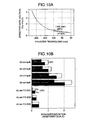
- FIG. 10A illustrates the relationship between V DD -V T0 and fine-patterning process technology.
- V DD -V T0 denotes effective gate voltage (i.e., gate-over drive voltage) of the MOST
- V T0 denotes average V T of the MOST.
- ITRS 2001 International Technology Roadmap for Semiconductors, 2001 ed .
- MPU and LPSOC denote a microprocessor and a low-power System On a Chip, respectively.
- a lower-limit exists to this V T0 .
- sub-threshold current i.e., a kind of leakage current
- This lower-limit value is determined by an upper-limit value of the leakage current on the chip.
- this lower-limit value is equal to an order of 0.2 V to 0.3 V in the case of a high-speed chip, and an order of 0.5 V in the case of a low-power chip. Accordingly, as illustrated in the drawing, the effective gate voltage quickly lowers in accompaniment with the fine patterning. This results in a rapid lowering in operation speed of MOSTs within a load-driving circuit. This is because the operation speed of a MOST is substantially inverse proportional to the effective gate voltage. For example, in the case of the high-speed chip, V DD lowers in accompaniment with the fine patterning, thus getting closer to 0.3 V. At this time, the circuit speed is delayed rapidly.
- Fig. 10B illustrates a drawing issued in M. Yamaoka et al., "Low Power SRAM Menu for SOC Application Using Yin-Yang-Feedback Memory Cell Technology", Symp. VLSI Circuits Dig., pp. 288 to 291, June 2004 .
- standard deviation ⁇ of the variation in the threshold voltage V T increases in accompaniment with finer patterning of the MOST.
- ⁇ int denotes standard deviation of the so-called intrinsic V T which is determined by a variation in the number of impurity atoms within channel of the MOST or a variation in the position thereof
- ⁇ ext denotes standard deviation of the so-called extrinsic V T which is determined by a variation in size of the channel or the like.
- the entire V T variation ⁇ is determined by both of the variations. Even in the case where the fine-patterning technology employed is of an order of 90 nm, ⁇ attains to as much as an order of 30 mV.
- the design of a single chip needs to be performed by taking into consideration the V T variation ( ⁇ V T ) of an order of 5 ⁇ , and this value attains to as much as 150 mV.
- the effective gate voltage of each MOST within the single chip which is represented by V DD -(V T0+ ⁇ V T ), turns out to be significantly varied.
- FD-SOI fully-depleted double-gate SOI (: Silicon-On-Insulator) MOST makes it possible to simultaneously satisfy these two conditions.
- FD-SOI fully-depleted double-gate SOI
- the FD-SOI structure itself allows reductions in the variation in the threshold voltage V T .
- taking advantage of this FD-SOI structure in a circuit-mannered configuration makes it possible to implement the dynamic V T as is described above.
- Fig. 11A, Fig. 11B, and Fig. 11C are an A-A cross-sectional view and a plan view of an N-channel MOST (NMOST) and a P-channel MOST (PMOST), and a B-B cross-sectional view of the NMOST, respectively. Also, Fig.
- Fig. 12A and Fig. 12B illustrate an equivalent circuit to the NMOST and a one to the PMOST, respectively.
- Fig. 11C indicates an example where the gate and the well are connected to each other.
- the reference numerals denote the following configuration components: 20 denotes a metal-silicide (such as NiSi) gate electrode, 3 denotes a single-crystal semiconductor thin film (i.e., SOI layer), 13 and 14 denote junction-capacitance-reducing n-type impurity diffusion layers, 8 denotes a high-concentration n-type impurity ultra-thin source diffusion layer, 9 denotes a high-concentration n-type impurity ultra-thin drain diffusion layer, 4 denotes a BOX (: Buried OXide) layer, 25 and 26 denote threshold-voltage control diffusion layers (i.e., well layers), and the like.
- 20 denotes a metal-silicide (such as NiSi) gate electrode
- 3 de
- the threshold voltage V T can be controlled based on type of the gate material, concentration of the well layer under the BOX layer, and voltage to be applied to the well layer.
- channel length (Lg) is equal to 100 nm or less
- the gate material is, e.g., the metal silicide such as nickel silicide (NiSi)
- thickness of the SOI layer which allows the MOST to be formed is equal to 20 nm or less
- thickness of the BOX layer is equal to 10 nm or less
- the concentration of the well layer located under the BOX layer is equal to an order of 10 16 cm -3 to 10 18 cm -3 .
- the employment of the thin BOX film or the like makes it possible to reduce the variation in V T of the FD-SOI MOST down to 20 % or less in the conventional bulk structure.
- the above-described double-gate MOST structure can be regarded as a single MOST which results from connecting an upper MOST and a lower MOST in parallel.
- the well layer becomes a gate
- the BOX layer becomes a gate insulating film. Accordingly, changing the well voltage in the lower MOST makes it possible to significantly change the entire threshold voltage V T of the double-gate MOST. This is because the well layer is insulated from the other components and thus the well voltage can be significantly changed without causing pn-junction leakage current to occur.
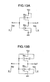
- Fig. 13A and Fig. 13B illustrate a conventional circuit which utilizes this characteristic. For example, in the well-known CMOS inverter illustrated in Fig.
- V T is dynamically changed depending on the circuit input, i.e., the gate voltage V DD of the MOST.
- the well voltage becomes equal to 0 V, which is small.
- V T becomes larger.
- the well voltage becomes higher.
- V T becomes smaller.
- V T is selected in advance as being large enough so that the sub-threshold current at the OFF time will become smaller than a tolerance value. Then, at the ON time, the effective gate voltage will become larger by the amount by which V T has become smaller.
- SRAM Static Random-Access Memory
- US 6 043 536 A discloses a method for operating a semiconductor device, which comprises: a first circuit and a second circuit, said first circuit and said second circuit including a MOS transistor having silicon-on-insulator structure, said silicon-on-insulator structure including double gates and an in dependence on a dynamically changing threshold voltage fully-depletable silicon-on-insulator layer, said double gates being a first gate and a second gate, said second gate being a well layer which exists under a buried oxide film, wherein said second circuit controls an input-voltage applied to said second gate of said MOS transistor inside said first circuit, and an output voltage of the second circuit is applied to the second gate of the MOS transistor in the first circuit, and a difference between a highest voltage and a lowest voltage of the output-voltage from said second circuit is larger than a difference between a highest voltage and a lowest voltage of the input-voltage into said first circuit, an amplitude of the output-voltage having the same polarity as an amplitude of the input-voltage into said first circuit
- US 6 404 243 B1 discloses a floating body architecture CMOSFET inverter with body biasing inverters added for controlling the delay time of the inverter. At least one body biasing inverter is connected between the main inverter's input and the body terminals of the FETs of the inverter. By supplying a representation of the input voltage to the body terminals of the p-channel and the n-channel FETs the inverter is able to control the history-dependent delay time associated with the variable source-to-body voltages in floating body CMOSFET inverters.
- this object is accomplished with a method of operating a semiconductor device having the features of claim 1.
- Fig. 1 illustrates a CMOS inverter circuit which is a first embodiment of the present invention.
- a first circuit includes, e.g., an inverter INV
- a second circuit includes, e.g., a converter CNV for controlling well voltages with large voltage amplitudes.
- the second circuit is a sub-circuit.
- This sub-circuit drives comparatively small well capacities of MOSTs within the first circuit, and thus is easy to design into small-size, high-speed, and low power-consumption implementation.
- the first circuit is a main-circuit.
- This main-circuit must generically drive large load capacities, and thus cannot help being formed into large-area, low-speed, and large power-consumption implementation. Consequently, adding the second circuit to the first one results in exertion of only a small influence on the entire area, speed, and power consumption.
- a PMOST (M P1 ) and an NMOST (M N1 ) are the FD-SOI MOST illustrated in Fig. 11 and Fig. 12 .
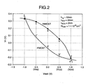
- Fig. 2 illustrates the relationship of the threshold voltages V T of these MOSTs relative to the well voltages.
- V T are the values defined using a constant current (1 nA/ ⁇ m).
- V T the polarity becomes inverted to that of the NMOST.
- the threshold voltages V T are measured in compliance with ordinary conditions, and V T of the NMOST measured when the well voltage is set at 0 V is equal to 0.2 V, and V T of the PMOST measured when the well voltage is set at V DD is also equal to substantially 0.2 V.
- the converter CNV converts a pulse, which is inputted into an input terminal IN and whose amplitude is equal to V DD , into a same-polarity pulse which is provided with a larger amplitude ranging from V BB to V DH .
- the converter CNV applies this same-polarity and larger-amplitude pulse to the wells of M P1 and M N1 .
- V T threshold voltage
- V DD 0.5 V
- V BB -0.5 V
- V DH 1 V
- V T changes to a point d in the drawing where V T is smaller.
- the NMOST finds it possible to drive (i.e., discharge) load capacity of an output terminal OUT at high speed and with a large current.
- the PMOST is switched OFF. This is because, since the well voltage of the PMOST also becomes equal to V DH , its V T changes to a point d' in the drawing, and thus the PMOST changes into an enhancement mode where V T is larger.
- the input pulse changes from V DD to 0 V
- the output of the converter changes from V DH to V BB .
- the NMOST changes from the point d to a point c, thus changing into an enhancement mode where V T is substantially equal to 0.3 V.
- the PMOST transitions from the point d' to a point c', thus changing into a depletion mode where V T is substantially equal to 0.1 V. Consequently, this time, the PMOST will drive (i.e., charge) the load capacity of the output terminal OUT at high speed and with a large current that the PMOST has generated.
- V DH and V BB can be generated based on the power-supply voltage V DD and using a charge-pump circuit, for example.
- the threshold voltages V T of the MOSTs change dynamically with the intervention of the converter CNV.
- V IN conversion ratio of the input voltage (V IN ) into the well voltage (V well )
- k 2 change ratio of V T in response to the change in the well voltage
- the input voltage at which the NMOST starts to be switched ON becomes smaller by the amount of coefficient (1 + k 1 k 2 ).
- this very input voltage which is none other than V T of the NMOST generated as the result of the dynamic change, indicates that the input voltage has become smaller.
- the input voltage at which the NMOST starts to be switched ON can be determined from the expression (1) in basically the same way. Namely, the NMOST is permitted to operate at the input voltages of the following ascending order, i.e., 0.28 V in the converter intervention scheme, 0.36 V in the gate-well direct connection scheme, and 0.5 V in the well-voltage fixed scheme.
- the change ratio k 2 of V T relative to the well voltage be larger in order to enhance the effect of the dynamic V T like this.
- V T 0 - k 2 ⁇ V well V T 0 - k 1 ⁇ k 2 ⁇ V IN ⁇ 0.
- films such as oxynitride (SiON) film are also preferable.
- SiON oxynitride
- the gate-film interface maintains stability even at a high-temperature processing temperature needed after formation of the BOX layer.
- the BOX layer can be made thin down to an order of 1.5 nm in equivalent silicon-dioxide thickness. The operation and effect explained so far are also basically the same in the case of the PMOST.
- the second circuit (converter CNV) is highly-sensitive and highly-speedy enough to detect an infinitesimal change in the input voltage
- V T (0) 0.5 V
- the minimum voltage which permits the MOSTs within the first circuit to operate is equal to 0.5 V in the well-voltage fixed scheme, 0.36 V in the gate-well direct connection scheme, and 0.28 V in the converter scheme. This shows that, even if V DD has lowered down to an order of 3 V, the converter scheme permits the operation although the other two schemes do not permit the operation.
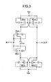
- Fig. 3 illustrates a concrete example of the high-sensitivity and high-speed converter (CNV).
- CNV high-sensitivity and high-speed converter
- the threshold voltages V T change dynamically.
- the wells and circuits of M P22 , M P23 , M N22 , and M N23 are operated with larger voltage amplitudes which differ from voltage amplitude at the wells of the MOSTs (M N21 , M P21 ) within the input circuit.
- variations in the threshold voltages V T of the feedback MOSTs are larger by the amount equivalent thereto. This results in an advantage that the feedback effect is made even larger. For example, if M N21 is switched ON at the input voltage smaller than V DD , gate voltage of M P23 lowers, and thus an output OUT' starts to be charged up to V DH .
- V T changes in the range of the point a to the point b
- V P21 changes in the range of the point a' to the point b'. Accordingly, the variations in V T are smaller by the amount of the smaller change in the gate input voltage.
- V T change in the range of the point c' to the point d'
- M N22 and M N23 V T change in the range of the point c to the point d.
- V T the variations in V T are larger by the amount of the larger change in the gate input voltage, i.e., the voltage change made from V DH to V BB .
- the input MOSTs (M N21 , M P21 ) are smaller than the feedback MOST circuits (M P22 and M P23 , M N22 and M N23 ) by the amount of the differences in the voltage amplitudes.
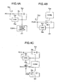
- Fig. 4A, Fig. 4B, and Fig. 4C illustrate as examples not forming part of the claimed invention power-supply switches to which a MOST whose well is driven with a large voltage amplitude is applied, and which are then made small-sized.
- a first circuit is a power-supply switch
- a second circuit is an internal core circuit (CORE).
- the operating voltage for the internal core circuit is small, and accordingly the threshold voltage V T of the MOST is also small. This results in flowing of a large sub-threshold current therein.
- Fig. 4A, Fig. 4B, and Fig. 4C illustrate as examples not forming part of the claimed invention power-supply switches to which a MOST whose well is driven with a large voltage amplitude is applied, and which are then made small-sized.
- a first circuit is a power-supply switch
- a second circuit is an internal core circuit (CORE).
- the operating voltage for the internal core circuit is small, and accordingly the threshold voltage
- V T of the PMOST is made larger.
- feeding an enough ON-current to the internal core circuit requires that V T of the PMOST be made small enough.
- the characteristic is as follows: Namely, the well voltage amplitude of the switch MOST is made larger than the gate input-voltage amplitude of the switch MOST, or the well voltage amplitude of the switch MOST is made larger than the drain voltage amplitude or source voltage amplitude of the switch MOST.
- channel width of the switch PMOST attains to 3 ⁇ m or more.
- V T at the ON time of the MOST is made smaller, the current feeding capability will be enhanced.
- the threshold voltages V T is the value which is always fixed. This condition makes V T at the OFF time smaller as well, thereby making it impossible to shield the MOST. As a result, the sub-threshold current in the MOST becomes a problem.
- V T of the MOST can be made larger at the OFF time. Accordingly, it becomes possible to shield the MOST completely. Also, V T of the MOST can be made smaller at the ON time. Consequently, it becomes possible to feed the enough current to the internal core circuit even if the channel width of the MOST is narrower. Since the internal core circuit generally occupies a large area, an area increase by the converter CNV is negligible.
- Fig. 4B illustrates an example where the NMOST (M N ) is used as the switch MOST. This embodiment is expected to exhibit basically the same effect.
- Fig. 4C illustrates an example where the switches are used on both of the power-supply side and the ground side. If the output from the converter CNV is inverted by an inverter and is applied to M N , setting up only one converter will suffice.
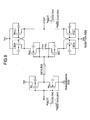
- Fig. 5A illustrates as an example not forming part of the claimed invention a MOST switch (i.e., first circuit) and a repetition-circuit block (BLK) (i.e., second circuit).
- this repetition-circuit block is, e.g., a word-driver block of memory.
- Each MOST included therein is the FD-SOI MOST.
- the respective sources of output PMOSTs (M W ) of inverters are collectively connected to a single common source line PWL.
- the PWL is connected to power-supply voltage V DD via the switch MOST (M P ).
- the switch MOST (M P ) is switched ON, and the input voltage into one inverter INV out of the n inverters within the block BLK is made equal to 0 V.
- This operation selects the one inverter INV, thus selecting and driving the corresponding one word line from among n word lines (i.e., WL 0 , ..., WL n-1 ).
- the gate voltage of M P is made equal to V DD to switch M P OFF.
- the input voltages into all the inverters are made equal to V DD to switch all the inverters OFF.
- the switch MOST (M P ) is added to the block BLK in order to reduce a sub-threshold current which will flow in the output PMOSTs (M W ) within the block BLK.
- the switch MOST (M P ) is added to the block BLK in order to reduce a sub-threshold current which will flow in the output PMOSTs (M W ) within the block BLK.
- the threshold voltages V T of all the MOSTs are equal to each other at the time of the non-selection
- the sub-threshold current will be reduced down to W P /nW by the switch MOST (M P ).
- W P and W denote channel width of the switch MOST (M P ) and that of the output PMOSTs (M W ) of the inverters.
- the present example results from adding, to the respective sub-blocks, the switch in Fig. 5A which is equipped with the selection function. Only a switch MOST corresponding to a sub-block wished to be selected is switched ON. As compared with the example in Fig. 5A , size of each switch MOST can be made smaller by the amount equivalent to the implementation of the division. Accordingly, well capacity of each switch MOST can be made smaller. Consequently, it is effective enough to select and drive a single switch MOST alone which has the small capacity like this. This allows implementation of the low power consumption.
- the examples not forming part of the claimed invention illustrated in Fig. 4A, Fig. 4B, Fig. 4C , Fig. 5A, and Fig. 5B are the ones where the power-supply switch illustrated in Fig. 6A is used.
- a power-supply switch is also usable where the gate and the well are directly connected to each other, and where a pulse whose amplitude is made equal to V DH and V BB is applied to this gate.
- the implementation of this large amplitude makes it possible to make the change in V T larger.
- the converter CNV for driving each MOST can be omitted. This allows implementation of the smaller area as a whole.
- Fig. 7A and Fig. 7B illustrate amplifiers which result from taking advantage of this amplification effect exhibited by the conventional circuit.
- Fig. 7A illustrates a latch sense amplifier used in such devices as a DRAM (: Dynamic Random-Access Memory).
- DRAM Dynamic Random-Access Memory
- the gates and the wells are directly connected to each other. This makes the input voltage effectively larger; that is to say, the amplification effect exists effectively.
- One (in1) of inputs is equal to V DD /2-V s , which results from superimposing a signal voltage v s on a floating voltage V DD /2, and the other input (in2) is equal to the floating voltage V DD /2.
- well voltages of the NMOSTs i.e., M N1 and M N2
- V T of M N2 becomes larger by ⁇ V T by the negative signal voltage v s . Namely, by the amount of ⁇ V T , M N2 finds it more difficult to be switched ON.
- Fig. 7B illustrates a well-known current-mirror amplifier frequently used in such devices as a SRAM. This current-mirror amplifier also effectively exhibits the amplification effect in basically the same way.
- V REF denotes reference voltage.
- Fig. 8 illustrates a DRAM sense system where NMOST version of the power-supply switch illustrated in Fig. 6B and the amplifier illustrated in Fig. 7A are combined with each other.
- a negative signal voltage v s will be outputted to one of the data pair-lines (e.g., DL 0 and /DL 0 ) which are precharged at the voltage V DD /2.
- this signal voltage is equal to an order of 100 mV, which is considerably small.
- this signal voltage is amplified up to V DD by using a latch CMOS sense amplifier (: SA) where the well-known cross-connected NMOS amplifier and PMOS amplifier as illustrated in Fig. 7A are longitudinally accumulated.
- SA CMOS sense amplifier
- Switching the driving MOSTs (i.e., M ND and M PD ) ON allows the amplification to be started.
- the amplification is performed at first using the NMOS amplifier by switching M ND ON, and after that, the amplification is subsequently performed using the PMOS amplifier by switching M PD ON.
- the data line (/DL 0 in the drawing) which is charged at the larger initial voltage will be charged up to V DD
- the data line (DL 0 ) which is charged at the smaller initial voltage will be discharged down to 0 V.
- the threshold voltage V T of M N2 becomes larger. Accordingly, if M ND is switched ON, the data line DL 0 starts to be discharged toward 0 V. After that, if M PD is switched ON, V T of M P2 becomes smaller since DL 0 is being discharged.
- M P2 will charge the data line /DL 0 even further.
- the driving MOSTs are driven with the large voltage amplitudes.
- V T at the time of the operation can be made small enough with V T at the time of the non-operation being maintained at constant large values. This, at the time of the operation, allows the amplifiers to be driven at high speed.
- Fig. 9 illustrates a CMOS inverter which takes advantage of circuits where the gates and the wells are directly connected to each other.
- the present example not forming part of the claimed invention is one which allows an extraordinarily large load capacity of device, such as data bus inside a chip, to be driven with low power consumption and at high speed.
- driving the large load capacity at a low voltage is advantageous from the point-of-view of the low power consumption.
- this method results in a lowering in the operation speed.
- the internal main circuits are driven with an amplitude of 1 V ranging from V DH (1V) to V BB (0V).
- the internal large bus capacity is driven with an amplitude of 0.5 V ranging from V DD (0.75 V) to V SH (0.25 V).
- the in-inverter MOSTs on the transmission side inside the chip are driven with the large logic amplitude.
- V T the changes in V T are significantly large.
- V DD and V SH are set between V DH and V BB .
- V BB in this embodiment is set not at the negative voltage but at the ground level.
- the reason for this is as follows: Namely, generating the negative voltage inside the chip necessitates the use of a charge-pump circuit, but the charge-pump circuit lacks in its current driving capability. This situation makes it difficult to drive the large load capacity such as the data bus with the use of V BB which is at the stable level.
- the direct connection between the gates and the wells is the same as in the conventional circuit, there exist the following differences: Namely, the well voltage amplitudes are larger than the drain voltage amplitudes or source voltage amplitudes. Otherwise, the well voltage amplitudes of the in-first-circuit MOSTs on the transmission side are different from the well voltage amplitudes on the reception side.
- the input signal is inputted into the gate of the upper MOST, and the threshold voltage V T of the entire MOST is controlled using the control voltage inputted into the well in the lower MOST.
- These functions can also be made reverse. Namely, a circuit scheme is also possible where the input signal is inputted into the well, and where the control voltage for V T is inputted into the gate of the upper MOST.
Landscapes
- Engineering & Computer Science (AREA)
- Computer Hardware Design (AREA)
- Power Engineering (AREA)
- Physics & Mathematics (AREA)
- Microelectronics & Electronic Packaging (AREA)
- Condensed Matter Physics & Semiconductors (AREA)
- General Physics & Mathematics (AREA)
- General Engineering & Computer Science (AREA)
- Mathematical Physics (AREA)
- Computing Systems (AREA)
- Ceramic Engineering (AREA)
- Manufacturing & Machinery (AREA)
- Metal-Oxide And Bipolar Metal-Oxide Semiconductor Integrated Circuits (AREA)
- Dram (AREA)
- Thin Film Transistor (AREA)
- Logic Circuits (AREA)
Claims (4)
- Procédé de fonctionnement pour un dispositif semi-conducteur, qui comprend :un premier circuit (INV) et un second circuit (CNV),ledit premier circuit (INV) et ledit second circuit (CNV) incluant un transistor MOS ayant une structure de silicium sur isolant, ladite structure de silicium sur isolant incluant des doubles grilles etune couche de silicium sur isolant entièrement appauvrie (3) dépendant d'une tension de seuil qui change de manière dynamique, lesdites doubles grilles étant une première grille (20) et une seconde grille (25), ladite seconde grille (25) étant une couche de puits qui existe sous un film d'oxyde enterré (4),dans lequelledit second circuit (CNV) commande une tension d'entrée appliquée à ladite seconde grille (25) dudit transistor MOS à l'intérieur dudit premier circuit (INV) et une tension de sortie du second circuit (CNV) est appliquée à la seconde grille (25) du transistor MOS dans le premier circuit (INV),caractérisé en ce queune différence entre une tension maximale (VDH) et une tension minimale (VBB) de la tension de sortie dudit second circuit (CNV) est supérieure à une différence entre une tension maximale (VDD) et une tension minimale (0) de la tension d'entrée dans ledit premier circuit (INV), une amplitude de la tension de sortie ayant la même polarité qu'une amplitude de la tension d'entrée dans ledit premier circuit,ladite tension d'entrée dans ledit premier circuit (INV) est appliquée à la première grille (20) du transistor MOS dans le premier circuit (INV) et ladite tension appliquée à ladite seconde grille (25) dudit transistor MOS à l'intérieur dudit premier circuit (INV) est commandée de telle sorte que la tension de seuil (VT) dudit transistor MOS diminue au moment de sa conduction et augmente au moment de sa non-conduction.
- Le procédé selon la revendication 1, dans lequel ledit second circuit (CNV) inclut ledit transistor MOS où ladite première grille (20) et ladite seconde grille (25) sont reliées directement l'une à l'autre.
- Le procédé selon la revendication 1, dans lequel une première grille (20) et une seconde grille (25) dudit transistor MOS (MN21, MP21) dudit second circuit (CNV) sont reliées l'une à l'autre.
- Le procédé selon la revendication 1, dans lequel la tension de seuil au moment de la non-conduction d'au moins ledit transistor MOS (MN21, MP21) à l'intérieur dudit second circuit (CNV) est inférieure à la tension de seuil au moment de la non-conduction dudit transistor MOS à l'intérieur dudit premier circuit (INV).
Priority Applications (2)
| Application Number | Priority Date | Filing Date | Title |
|---|---|---|---|
| EP10002248A EP2207202A1 (fr) | 2005-07-11 | 2006-02-27 | Dispositifs semi-conducteurs |
| EP10002249A EP2207203A1 (fr) | 2005-07-11 | 2006-02-27 | Dispositifs semi-conducteurs |
Applications Claiming Priority (2)
| Application Number | Priority Date | Filing Date | Title |
|---|---|---|---|
| JP2005201054A JP4967264B2 (ja) | 2005-07-11 | 2005-07-11 | 半導体装置 |
| EP06003938A EP1744364A3 (fr) | 2005-07-11 | 2006-02-27 | Dispositifs semi-conducteurs |
Related Parent Applications (2)
| Application Number | Title | Priority Date | Filing Date |
|---|---|---|---|
| EP06003938A Division EP1744364A3 (fr) | 2005-07-11 | 2006-02-27 | Dispositifs semi-conducteurs |
| EP06003938.5 Division | 2006-02-27 |
Related Child Applications (2)
| Application Number | Title | Priority Date | Filing Date |
|---|---|---|---|
| EP10002248.2 Division-Into | 2010-03-04 | ||
| EP10002249.0 Division-Into | 2010-03-04 |
Publications (3)
| Publication Number | Publication Date |
|---|---|
| EP2053657A2 EP2053657A2 (fr) | 2009-04-29 |
| EP2053657A3 EP2053657A3 (fr) | 2009-07-22 |
| EP2053657B1 true EP2053657B1 (fr) | 2012-11-07 |
Family
ID=36972724
Family Applications (4)
| Application Number | Title | Priority Date | Filing Date |
|---|---|---|---|
| EP09001297A Expired - Fee Related EP2053657B1 (fr) | 2005-07-11 | 2006-02-27 | Procédé de fonctionnement pour un dispositif semi-conducteur |
| EP10002248A Withdrawn EP2207202A1 (fr) | 2005-07-11 | 2006-02-27 | Dispositifs semi-conducteurs |
| EP06003938A Withdrawn EP1744364A3 (fr) | 2005-07-11 | 2006-02-27 | Dispositifs semi-conducteurs |
| EP10002249A Withdrawn EP2207203A1 (fr) | 2005-07-11 | 2006-02-27 | Dispositifs semi-conducteurs |
Family Applications After (3)
| Application Number | Title | Priority Date | Filing Date |
|---|---|---|---|
| EP10002248A Withdrawn EP2207202A1 (fr) | 2005-07-11 | 2006-02-27 | Dispositifs semi-conducteurs |
| EP06003938A Withdrawn EP1744364A3 (fr) | 2005-07-11 | 2006-02-27 | Dispositifs semi-conducteurs |
| EP10002249A Withdrawn EP2207203A1 (fr) | 2005-07-11 | 2006-02-27 | Dispositifs semi-conducteurs |
Country Status (6)
| Country | Link |
|---|---|
| US (2) | US7511558B2 (fr) |
| EP (4) | EP2053657B1 (fr) |
| JP (1) | JP4967264B2 (fr) |
| KR (1) | KR101106916B1 (fr) |
| CN (2) | CN101281929B (fr) |
| TW (1) | TW200723499A (fr) |
Cited By (1)
| Publication number | Priority date | Publication date | Assignee | Title |
|---|---|---|---|---|
| US9472559B2 (en) | 2009-12-28 | 2016-10-18 | Semiconductor Energy Laboratory Co., Ltd. | Memory device and semiconductor device |
Families Citing this family (46)
| Publication number | Priority date | Publication date | Assignee | Title |
|---|---|---|---|---|
| JP4800700B2 (ja) * | 2005-08-01 | 2011-10-26 | ルネサスエレクトロニクス株式会社 | 半導体装置およびそれを用いた半導体集積回路 |
| JP2007179602A (ja) * | 2005-12-27 | 2007-07-12 | Hitachi Ltd | 半導体装置 |
| TWI355664B (en) * | 2006-09-29 | 2012-01-01 | Macronix Int Co Ltd | Method of reading a dual bit memory cell |
| EP2118268B1 (fr) * | 2007-01-10 | 2015-07-08 | Hemoshear, LLC | Utilisation d'un modele de co-culture de cellules endotheliales/de muscles lisses hemodynamique in vitro pour identifier de nouvelles cibles therapeutiques pour les maladies vasculaires |
| TW200834525A (en) * | 2007-02-14 | 2008-08-16 | Advanced Analog Technology Inc | Image sticking erasing circuit, the method for performing the same and monitor control circuit thereof |
| JP2009088387A (ja) * | 2007-10-02 | 2009-04-23 | Renesas Technology Corp | 半導体装置 |
| JP5234333B2 (ja) * | 2008-05-28 | 2013-07-10 | Nltテクノロジー株式会社 | ゲート線駆動回路、アクティブマトリクス基板及び液晶表示装置 |
| KR101623958B1 (ko) * | 2008-10-01 | 2016-05-25 | 삼성전자주식회사 | 인버터 및 그의 동작방법과 인버터를 포함하는 논리회로 |
| US20100102872A1 (en) * | 2008-10-29 | 2010-04-29 | Taiwan Semiconductor Manufacturing Co., Ltd. | Dynamic Substrate Bias for PMOS Transistors to Alleviate NBTI Degradation |
| KR101034615B1 (ko) * | 2009-08-11 | 2011-05-12 | 주식회사 하이닉스반도체 | 센스앰프 및 이를 포함하는 반도체 메모리장치 |
| EP2320454A1 (fr) * | 2009-11-05 | 2011-05-11 | S.O.I.Tec Silicon on Insulator Technologies | Porte substrat et dispositif de serrage par clip |
| FR2953641B1 (fr) | 2009-12-08 | 2012-02-10 | S O I Tec Silicon On Insulator Tech | Circuit de transistors homogenes sur seoi avec grille de controle arriere enterree sous la couche isolante |
| FR2953643B1 (fr) | 2009-12-08 | 2012-07-27 | Soitec Silicon On Insulator | Cellule memoire flash sur seoi disposant d'une seconde grille de controle enterree sous la couche isolante |
| US8508289B2 (en) | 2009-12-08 | 2013-08-13 | Soitec | Data-path cell on an SeOI substrate with a back control gate beneath the insulating layer |
| FR2957193B1 (fr) | 2010-03-03 | 2012-04-20 | Soitec Silicon On Insulator | Cellule a chemin de donnees sur substrat seoi avec grille de controle arriere enterree sous la couche isolante |
| FR2953636B1 (fr) * | 2009-12-08 | 2012-02-10 | Soitec Silicon On Insulator | Procede de commande d'une cellule memoire dram sur seoi disposant d'une seconde grille de controle enterree sous la couche isolante |
| FR2955200B1 (fr) | 2010-01-14 | 2012-07-20 | Soitec Silicon On Insulator | Dispositif, et son procede de fabrication, disposant d'un contact entre regions semi-conductrices a travers une couche isolante enterree |
| FR2955204B1 (fr) | 2010-01-14 | 2012-07-20 | Soitec Silicon On Insulator | Cellule memoire dram disposant d'un injecteur bipolaire vertical |
| FR2955203B1 (fr) | 2010-01-14 | 2012-03-23 | Soitec Silicon On Insulator | Cellule memoire dont le canal traverse une couche dielectrique enterree |
| FR2955195B1 (fr) | 2010-01-14 | 2012-03-09 | Soitec Silicon On Insulator | Dispositif de comparaison de donnees dans une memoire adressable par contenu sur seoi |
| FR2957186B1 (fr) | 2010-03-08 | 2012-09-28 | Soitec Silicon On Insulator | Cellule memoire de type sram |
| FR2957449B1 (fr) | 2010-03-11 | 2022-07-15 | S O I Tec Silicon On Insulator Tech | Micro-amplificateur de lecture pour memoire |
| FR2958441B1 (fr) | 2010-04-02 | 2012-07-13 | Soitec Silicon On Insulator | Circuit pseudo-inverseur sur seoi |
| EP2372716A1 (fr) * | 2010-04-02 | 2011-10-05 | S.O.I.Tec Silicon on Insulator Technologies | Circuit pseudo-inverseur sur SeOI |
| EP2378549A1 (fr) | 2010-04-06 | 2011-10-19 | S.O.I.Tec Silicon on Insulator Technologies | Procédé de fabrication d'un substrat semi-conducteur |
| EP2381470B1 (fr) | 2010-04-22 | 2012-08-22 | Soitec | Dispositif semi-conducteur comprenant un transistor à effet de champ dans une structure silicium sur isolant |
| US8988152B2 (en) * | 2012-02-29 | 2015-03-24 | Semiconductor Energy Laboratory Co., Ltd. | Semiconductor device |
| US8624632B2 (en) | 2012-03-29 | 2014-01-07 | International Business Machines Corporation | Sense amplifier-type latch circuits with static bias current for enhanced operating frequency |
| US10147724B2 (en) | 2012-07-07 | 2018-12-04 | Skyworks Solutions, Inc. | Feed-forward circuit to improve intermodulation distortion performance of radio-frequency switch |
| US8975950B2 (en) | 2012-07-07 | 2015-03-10 | Skyworks Solutions, Inc. | Switching device having a discharge circuit for improved intermodulation distortion performance |
| US9628075B2 (en) | 2012-07-07 | 2017-04-18 | Skyworks Solutions, Inc. | Radio-frequency switch having dynamic body coupling |
| US9276570B2 (en) | 2012-07-07 | 2016-03-01 | Skyworks Solutions, Inc. | Radio-frequency switch having gate node voltage compensation network |
| US9160328B2 (en) | 2012-07-07 | 2015-10-13 | Skyworks Solutions, Inc. | Circuits, devices, methods and applications related to silicon-on-insulator based radio-frequency switches |
| US9148194B2 (en) | 2012-07-07 | 2015-09-29 | Skyworks Solutions, Inc. | Radio-frequency switch system having improved intermodulation distortion performance |
| US9059702B2 (en) | 2012-07-07 | 2015-06-16 | Skyworks Solutions, Inc. | Switch linearization by non-linear compensation of a field-effect transistor |
| FR2999802A1 (fr) | 2012-12-14 | 2014-06-20 | St Microelectronics Sa | Cellule cmos realisee dans une technologie fd soi |
| US9013225B2 (en) | 2013-02-04 | 2015-04-21 | Skyworks Solutions, Inc. | RF switches having increased voltage swing uniformity |
| US8803591B1 (en) * | 2013-11-06 | 2014-08-12 | Freescale Semiconductor, Inc. | MOS transistor with forward bulk-biasing circuit |
| US20150129967A1 (en) * | 2013-11-12 | 2015-05-14 | Stmicroelectronics International N.V. | Dual gate fd-soi transistor |
| US9178517B2 (en) * | 2013-11-12 | 2015-11-03 | Stmicroelectronics International N.V. | Wide range core supply compatible level shifter circuit |
| US9800204B2 (en) | 2014-03-19 | 2017-10-24 | Stmicroelectronics International N.V. | Integrated circuit capacitor including dual gate silicon-on-insulator transistor |
| FR3034930B1 (fr) * | 2015-04-10 | 2019-06-14 | Universite De Nice | Procede et dispositif d'auto-calibration de circuits multi-grilles |
| US9972395B2 (en) * | 2015-10-05 | 2018-05-15 | Silicon Storage Technology, Inc. | Row and column decoders comprising fully depleted silicon-on-insulator transistors for use in flash memory systems |
| US10294968B2 (en) * | 2016-10-21 | 2019-05-21 | Thomas Joseph Hoey | Article retaining device and method of attachment |
| US10469076B2 (en) * | 2016-11-22 | 2019-11-05 | The Curators Of The University Of Missouri | Power gating circuit utilizing double-gate fully depleted silicon-on-insulator transistor |
| US11062745B2 (en) * | 2018-09-27 | 2021-07-13 | Taiwan Semiconductor Manufacturing Company, Ltd. | FDSOI sense amplifier configuration in a memory device |
Citations (1)
| Publication number | Priority date | Publication date | Assignee | Title |
|---|---|---|---|---|
| US6404243B1 (en) * | 2001-01-12 | 2002-06-11 | Hewlett-Packard Company | System and method for controlling delay times in floating-body CMOSFET inverters |
Family Cites Families (31)
| Publication number | Priority date | Publication date | Assignee | Title |
|---|---|---|---|---|
| US5604368A (en) * | 1994-07-15 | 1997-02-18 | International Business Machines Corporation | Self-aligned double-gate MOSFET by selective lateral epitaxy |
| US6072353A (en) * | 1995-04-26 | 2000-06-06 | Matsushita Electric Industrial Co., Ltd. | Logic circuit with overdriven off-state switching |
| US5736435A (en) * | 1995-07-03 | 1998-04-07 | Motorola, Inc. | Process for fabricating a fully self-aligned soi mosfet |
| JP3082671B2 (ja) * | 1996-06-26 | 2000-08-28 | 日本電気株式会社 | トランジスタ素子及びその製造方法 |
| TW324862B (en) * | 1996-07-03 | 1998-01-11 | Hitachi Ltd | Liquid display apparatus |
| US5831451A (en) * | 1996-07-19 | 1998-11-03 | Texas Instruments Incorporated | Dynamic logic circuits using transistors having differing threshold voltages |
| JP3195256B2 (ja) * | 1996-10-24 | 2001-08-06 | 株式会社東芝 | 半導体集積回路 |
| JPH10284729A (ja) * | 1997-02-07 | 1998-10-23 | Sony Corp | 絶縁ゲートトランジスタ素子及びその駆動方法 |
| JP3732914B2 (ja) * | 1997-02-28 | 2006-01-11 | 株式会社ルネサステクノロジ | 半導体装置 |
| US6037808A (en) * | 1997-12-24 | 2000-03-14 | Texas Instruments Incorporated | Differential SOI amplifiers having tied floating body connections |
| US6121659A (en) * | 1998-03-27 | 2000-09-19 | International Business Machines Corporation | Buried patterned conductor planes for semiconductor-on-insulator integrated circuit |
| JP3699823B2 (ja) | 1998-05-19 | 2005-09-28 | 株式会社東芝 | 半導体装置 |
| US6365465B1 (en) * | 1999-03-19 | 2002-04-02 | International Business Machines Corporation | Self-aligned double-gate MOSFET by selective epitaxy and silicon wafer bonding techniques |
| JP4439031B2 (ja) * | 1999-04-15 | 2010-03-24 | 株式会社ルネサステクノロジ | 半導体装置 |
| US6239649B1 (en) * | 1999-04-20 | 2001-05-29 | International Business Machines Corporation | Switched body SOI (silicon on insulator) circuits and fabrication method therefor |
| CN1139317C (zh) * | 1999-07-09 | 2004-02-25 | 北京锦绣大地农业股份有限公司 | 猪笼草工厂化快繁方法 |
| JP2001044441A (ja) * | 1999-07-29 | 2001-02-16 | Sony Corp | 完全空乏soi型半導体装置及び集積回路 |
| JP2002164544A (ja) * | 2000-11-28 | 2002-06-07 | Sony Corp | 半導体装置 |
| US6686630B2 (en) * | 2001-02-07 | 2004-02-03 | International Business Machines Corporation | Damascene double-gate MOSFET structure and its fabrication method |
| JP3729082B2 (ja) * | 2001-04-25 | 2005-12-21 | 日本電信電話株式会社 | 半導体保護回路 |
| US6433609B1 (en) * | 2001-11-19 | 2002-08-13 | International Business Machines Corporation | Double-gate low power SOI active clamp network for single power supply and multiple power supply applications |
| JP2003152192A (ja) * | 2001-11-19 | 2003-05-23 | Sony Corp | 電界効果半導体装置及びその駆動方法 |
| JP2004297048A (ja) * | 2003-03-11 | 2004-10-21 | Semiconductor Energy Lab Co Ltd | 集積回路、該集積回路を有する半導体表示装置及び集積回路の駆動方法 |
| US6919647B2 (en) * | 2003-07-03 | 2005-07-19 | American Semiconductor, Inc. | SRAM cell |
| US7019342B2 (en) * | 2003-07-03 | 2006-03-28 | American Semiconductor, Inc. | Double-gated transistor circuit |
| JP2005116981A (ja) * | 2003-10-10 | 2005-04-28 | Hitachi Ltd | 半導体装置 |
| JP3718512B2 (ja) * | 2003-10-24 | 2005-11-24 | 株式会社ルネサステクノロジ | 半導体装置 |
| JP2005201054A (ja) | 2004-01-13 | 2005-07-28 | Koyo Seiko Co Ltd | ポンプ |
| JP4795653B2 (ja) * | 2004-06-15 | 2011-10-19 | ルネサスエレクトロニクス株式会社 | 半導体記憶装置 |
| US7091069B2 (en) * | 2004-06-30 | 2006-08-15 | International Business Machines Corporation | Ultra thin body fully-depleted SOI MOSFETs |
| JP2006165808A (ja) * | 2004-12-03 | 2006-06-22 | Seiko Epson Corp | 差動増幅回路 |
-
2005
- 2005-07-11 JP JP2005201054A patent/JP4967264B2/ja not_active Expired - Fee Related
-
2006
- 2006-02-27 EP EP09001297A patent/EP2053657B1/fr not_active Expired - Fee Related
- 2006-02-27 EP EP10002248A patent/EP2207202A1/fr not_active Withdrawn
- 2006-02-27 KR KR1020060018925A patent/KR101106916B1/ko not_active IP Right Cessation
- 2006-02-27 EP EP06003938A patent/EP1744364A3/fr not_active Withdrawn
- 2006-02-27 EP EP10002249A patent/EP2207203A1/fr not_active Withdrawn
- 2006-02-27 US US11/362,172 patent/US7511558B2/en not_active Expired - Fee Related
- 2006-02-27 TW TW095106628A patent/TW200723499A/zh unknown
- 2006-02-28 CN CN2008100868803A patent/CN101281929B/zh not_active Expired - Fee Related
- 2006-02-28 CN CNB2006100093694A patent/CN100511688C/zh not_active Expired - Fee Related
-
2007
- 2007-03-07 US US11/714,844 patent/US7385436B2/en not_active Expired - Fee Related
Patent Citations (1)
| Publication number | Priority date | Publication date | Assignee | Title |
|---|---|---|---|---|
| US6404243B1 (en) * | 2001-01-12 | 2002-06-11 | Hewlett-Packard Company | System and method for controlling delay times in floating-body CMOSFET inverters |
Cited By (1)
| Publication number | Priority date | Publication date | Assignee | Title |
|---|---|---|---|---|
| US9472559B2 (en) | 2009-12-28 | 2016-10-18 | Semiconductor Energy Laboratory Co., Ltd. | Memory device and semiconductor device |
Also Published As
| Publication number | Publication date |
|---|---|
| US7511558B2 (en) | 2009-03-31 |
| EP2207202A1 (fr) | 2010-07-14 |
| KR20070007703A (ko) | 2007-01-16 |
| US20070152736A1 (en) | 2007-07-05 |
| US7385436B2 (en) | 2008-06-10 |
| KR101106916B1 (ko) | 2012-01-25 |
| EP1744364A3 (fr) | 2008-06-04 |
| EP2207203A1 (fr) | 2010-07-14 |
| TW200723499A (en) | 2007-06-16 |
| CN1897284A (zh) | 2007-01-17 |
| CN101281929A (zh) | 2008-10-08 |
| EP2053657A2 (fr) | 2009-04-29 |
| EP1744364A2 (fr) | 2007-01-17 |
| JP4967264B2 (ja) | 2012-07-04 |
| EP2053657A3 (fr) | 2009-07-22 |
| CN101281929B (zh) | 2010-10-13 |
| JP2007019357A (ja) | 2007-01-25 |
| CN100511688C (zh) | 2009-07-08 |
| US20070008027A1 (en) | 2007-01-11 |
Similar Documents
| Publication | Publication Date | Title |
|---|---|---|
| EP2053657B1 (fr) | Procédé de fonctionnement pour un dispositif semi-conducteur | |
| US8508283B2 (en) | Semiconductor device with back-gate voltage control of a logic circuit | |
| EP0724295B1 (fr) | Dispositif semi-conducteur du type SOI ayant des tensions de seuil variables | |
| KR100288818B1 (ko) | 반도체 집적회로 | |
| JP3480830B2 (ja) | ドライバ回路 | |
| KR100308708B1 (ko) | 기생 바이폴라 전류 감소 방법 및 장치 | |
| US6232793B1 (en) | Switched backgate bias for FET | |
| US6504212B1 (en) | Method and apparatus for enhanced SOI passgate operations | |
| US20110102019A1 (en) | Semiconductor device formed on a soi substrate | |
| JP2939086B2 (ja) | 半導体装置 | |
| JP2004296795A (ja) | 二重ゲート電界効果トランジスタ | |
| US8077510B2 (en) | SRAM device | |
| US6211725B1 (en) | Low powder CMOS circuit | |
| JP2009524292A (ja) | 酸化物薄膜電界効果トランジスタを使用したデジタル出力ドライバおよび入力バッファー | |
| JP2006512005A (ja) | Nチャネルプルアップ素子および論理回路 | |
| JP3864243B2 (ja) | Soiドミノ回路内の寄生バイポーラ動作を除去する方法及びsoiドミノ回路 | |
| US6150869A (en) | Method and apparatus for body control in silicon-on-insulator (SOI) domino circuits | |
| US6917082B1 (en) | Gate-body cross-link circuitry for metal-oxide-semiconductor transistor circuits | |
| US11979145B1 (en) | Back bias control for always-on circuit section enabling leakage reduction during power saving mode |
Legal Events
| Date | Code | Title | Description |
|---|---|---|---|
| PUAI | Public reference made under article 153(3) epc to a published international application that has entered the european phase |
Free format text: ORIGINAL CODE: 0009012 |
|
| 17P | Request for examination filed |
Effective date: 20090130 |
|
| AC | Divisional application: reference to earlier application |
Ref document number: 1744364 Country of ref document: EP Kind code of ref document: P |
|
| AK | Designated contracting states |
Kind code of ref document: A2 Designated state(s): AT BE BG CH CY CZ DE DK EE ES FI FR GB GR HU IE IS IT LI LT LU LV MC NL PL PT RO SE SI SK TR |
|
| AX | Request for extension of the european patent |
Extension state: AL BA HR MK YU |
|
| PUAL | Search report despatched |
Free format text: ORIGINAL CODE: 0009013 |
|
| AK | Designated contracting states |
Kind code of ref document: A3 Designated state(s): AT BE BG CH CY CZ DE DK EE ES FI FR GB GR HU IE IS IT LI LT LU LV MC NL PL PT RO SE SI SK TR |
|
| AX | Request for extension of the european patent |
Extension state: AL BA HR MK YU |
|
| 17Q | First examination report despatched |
Effective date: 20090831 |
|
| AKX | Designation fees paid |
Designated state(s): BE DE FR |
|
| REG | Reference to a national code |
Ref country code: DE Ref legal event code: R079 Ref document number: 602006032984 Country of ref document: DE Free format text: PREVIOUS MAIN CLASS: H01L0027120000 Ipc: H01L0021840000 |
|
| RIC1 | Information provided on ipc code assigned before grant |
Ipc: H03K 19/0185 20060101ALI20120316BHEP Ipc: H01L 21/84 20060101AFI20120316BHEP Ipc: H03K 19/003 20060101ALI20120316BHEP Ipc: H03K 19/00 20060101ALI20120316BHEP Ipc: H01L 29/66 20060101ALI20120316BHEP Ipc: H01L 27/12 20060101ALI20120316BHEP |
|
| RTI1 | Title (correction) |
Free format text: METHOD FOR OPERATING A SEMICONDUCTOR DEVICE |
|
| GRAP | Despatch of communication of intention to grant a patent |
Free format text: ORIGINAL CODE: EPIDOSNIGR1 |
|
| RIN1 | Information on inventor provided before grant (corrected) |
Inventor name: TSUCHIYA, RYUTA Inventor name: KAWAHARA, TAKAYUKI Inventor name: ITOH, KIYOO |
|
| GRAS | Grant fee paid |
Free format text: ORIGINAL CODE: EPIDOSNIGR3 |
|
| GRAA | (expected) grant |
Free format text: ORIGINAL CODE: 0009210 |
|
| AC | Divisional application: reference to earlier application |
Ref document number: 1744364 Country of ref document: EP Kind code of ref document: P |
|
| AK | Designated contracting states |
Kind code of ref document: B1 Designated state(s): BE DE FR |
|
| REG | Reference to a national code |
Ref country code: DE Ref legal event code: R096 Ref document number: 602006032984 Country of ref document: DE Effective date: 20130103 |
|
| PG25 | Lapsed in a contracting state [announced via postgrant information from national office to epo] |
Ref country code: BE Free format text: LAPSE BECAUSE OF FAILURE TO SUBMIT A TRANSLATION OF THE DESCRIPTION OR TO PAY THE FEE WITHIN THE PRESCRIBED TIME-LIMIT Effective date: 20121107 |
|
| PLBE | No opposition filed within time limit |
Free format text: ORIGINAL CODE: 0009261 |
|
| STAA | Information on the status of an ep patent application or granted ep patent |
Free format text: STATUS: NO OPPOSITION FILED WITHIN TIME LIMIT |
|
| 26N | No opposition filed |
Effective date: 20130808 |
|
| REG | Reference to a national code |
Ref country code: FR Ref legal event code: ST Effective date: 20131031 |
|
| REG | Reference to a national code |
Ref country code: DE Ref legal event code: R097 Ref document number: 602006032984 Country of ref document: DE Effective date: 20130808 |
|
| PG25 | Lapsed in a contracting state [announced via postgrant information from national office to epo] |
Ref country code: FR Free format text: LAPSE BECAUSE OF NON-PAYMENT OF DUE FEES Effective date: 20130228 |
|
| PGFP | Annual fee paid to national office [announced via postgrant information from national office to epo] |
Ref country code: DE Payment date: 20160223 Year of fee payment: 11 |
|
| REG | Reference to a national code |
Ref country code: DE Ref legal event code: R119 Ref document number: 602006032984 Country of ref document: DE |
|
| PG25 | Lapsed in a contracting state [announced via postgrant information from national office to epo] |
Ref country code: DE Free format text: LAPSE BECAUSE OF NON-PAYMENT OF DUE FEES Effective date: 20170901 |