EP2037672B1 - Festkörper-bildgebungselement und bildgebungseinrichtung damit - Google Patents
Festkörper-bildgebungselement und bildgebungseinrichtung damit Download PDFInfo
- Publication number
- EP2037672B1 EP2037672B1 EP07744636.7A EP07744636A EP2037672B1 EP 2037672 B1 EP2037672 B1 EP 2037672B1 EP 07744636 A EP07744636 A EP 07744636A EP 2037672 B1 EP2037672 B1 EP 2037672B1
- Authority
- EP
- European Patent Office
- Prior art keywords
- photoelectric converter
- line
- converter portions
- electric charge
- pixel
- Prior art date
- Legal status (The legal status is an assumption and is not a legal conclusion. Google has not performed a legal analysis and makes no representation as to the accuracy of the status listed.)
- Ceased
Links
Images


Classifications
-
- H—ELECTRICITY
- H10—SEMICONDUCTOR DEVICES; ELECTRIC SOLID-STATE DEVICES NOT OTHERWISE PROVIDED FOR
- H10F—INORGANIC SEMICONDUCTOR DEVICES SENSITIVE TO INFRARED RADIATION, LIGHT, ELECTROMAGNETIC RADIATION OF SHORTER WAVELENGTH OR CORPUSCULAR RADIATION
- H10F39/00—Integrated devices, or assemblies of multiple devices, comprising at least one element covered by group H10F30/00, e.g. radiation detectors comprising photodiode arrays
- H10F39/80—Constructional details of image sensors
- H10F39/802—Geometry or disposition of elements in pixels, e.g. address-lines or gate electrodes
-
- H—ELECTRICITY
- H04—ELECTRIC COMMUNICATION TECHNIQUE
- H04N—PICTORIAL COMMUNICATION, e.g. TELEVISION
- H04N23/00—Cameras or camera modules comprising electronic image sensors; Control thereof
- H04N23/60—Control of cameras or camera modules
- H04N23/67—Focus control based on electronic image sensor signals
- H04N23/672—Focus control based on electronic image sensor signals based on the phase difference signals
-
- H—ELECTRICITY
- H04—ELECTRIC COMMUNICATION TECHNIQUE
- H04N—PICTORIAL COMMUNICATION, e.g. TELEVISION
- H04N25/00—Circuitry of solid-state image sensors [SSIS]; Control thereof
- H04N25/40—Extracting pixel data from image sensors by controlling scanning circuits, e.g. by modifying the number of pixels sampled or to be sampled
- H04N25/46—Extracting pixel data from image sensors by controlling scanning circuits, e.g. by modifying the number of pixels sampled or to be sampled by combining or binning pixels
-
- H—ELECTRICITY
- H04—ELECTRIC COMMUNICATION TECHNIQUE
- H04N—PICTORIAL COMMUNICATION, e.g. TELEVISION
- H04N25/00—Circuitry of solid-state image sensors [SSIS]; Control thereof
- H04N25/60—Noise processing, e.g. detecting, correcting, reducing or removing noise
- H04N25/62—Detection or reduction of noise due to excess charges produced by the exposure, e.g. smear, blooming, ghost image, crosstalk or leakage between pixels
- H04N25/621—Detection or reduction of noise due to excess charges produced by the exposure, e.g. smear, blooming, ghost image, crosstalk or leakage between pixels for the control of blooming
-
- H—ELECTRICITY
- H04—ELECTRIC COMMUNICATION TECHNIQUE
- H04N—PICTORIAL COMMUNICATION, e.g. TELEVISION
- H04N25/00—Circuitry of solid-state image sensors [SSIS]; Control thereof
- H04N25/70—SSIS architectures; Circuits associated therewith
- H04N25/702—SSIS architectures characterised by non-identical, non-equidistant or non-planar pixel layout
-
- H—ELECTRICITY
- H04—ELECTRIC COMMUNICATION TECHNIQUE
- H04N—PICTORIAL COMMUNICATION, e.g. TELEVISION
- H04N25/00—Circuitry of solid-state image sensors [SSIS]; Control thereof
- H04N25/70—SSIS architectures; Circuits associated therewith
- H04N25/703—SSIS architectures incorporating pixels for producing signals other than image signals
- H04N25/704—Pixels specially adapted for focusing, e.g. phase difference pixel sets
-
- H—ELECTRICITY
- H04—ELECTRIC COMMUNICATION TECHNIQUE
- H04N—PICTORIAL COMMUNICATION, e.g. TELEVISION
- H04N25/00—Circuitry of solid-state image sensors [SSIS]; Control thereof
- H04N25/70—SSIS architectures; Circuits associated therewith
- H04N25/76—Addressed sensors, e.g. MOS or CMOS sensors
- H04N25/77—Pixel circuitry, e.g. memories, A/D converters, pixel amplifiers, shared circuits or shared components
- H04N25/778—Pixel circuitry, e.g. memories, A/D converters, pixel amplifiers, shared circuits or shared components comprising amplifiers shared between a plurality of pixels, i.e. at least one part of the amplifier must be on the sensor array itself
-
- H—ELECTRICITY
- H10—SEMICONDUCTOR DEVICES; ELECTRIC SOLID-STATE DEVICES NOT OTHERWISE PROVIDED FOR
- H10F—INORGANIC SEMICONDUCTOR DEVICES SENSITIVE TO INFRARED RADIATION, LIGHT, ELECTROMAGNETIC RADIATION OF SHORTER WAVELENGTH OR CORPUSCULAR RADIATION
- H10F39/00—Integrated devices, or assemblies of multiple devices, comprising at least one element covered by group H10F30/00, e.g. radiation detectors comprising photodiode arrays
- H10F39/80—Constructional details of image sensors
- H10F39/813—Electronic components shared by multiple pixels, e.g. one amplifier shared by two pixels
Definitions
- the present invention relates to a solid-state imaging device and an imaging apparatus using the solid-state imaging device.
- an imaging apparatus such as a video camera and an electronic still camera has widely spread.
- a solid-state imaging device such as a CCD type and an amplification type is used.
- a plurality of pixels having a photoelectric converter portion for generating a signal charge in accordance with an amount of incident light are formed in a grid shape.
- a signal charge generated and accumulated by the photoelectric converter portion in a pixel is led to an amplifying portion, and a signal amplified by the amplifying portion is output from the pixel.
- an amplification type solid-state imaging device there is proposed, for example, a solid-state imaging device using a junction-field-effect-transistor in the amplifying portion in Japanese Patent Application Laid-Open Nos. 11-177076 and 2004-335882 , and a CMOS type solid-state imaging device using an MOS transistor in the amplifying portion in Japanese Patent Application Laid-Open No. 2004-111590 .
- a photoelectric converter portion, an amplifying portion, and a charge-storing portion for temporally storing the charge between them are disposed in each pixel.
- the signal charge generated in each photoelectric converter portion is transferred to each charge-storing portion at the same time over all pixels and temporally stored, and the signal charge is successively converted into pixel signal with a prescribed readout timing. Accordingly, it becomes possible to prevent image deformation caused by difference in exposure time of respective pixels between lines upon carrying out electronic shutter movement, which is a so-called rolling shutter.
- the pupil division phase difference detection method is a method for detecting a defocusing amount of an image-taking lens such that a bundle of rays passing through the image-taking lens is divided into two at pupil to form a pair of divided images, and difference in the images (the amount of phase shift) is detected.
- a plurality of pixels having photoelectric converter portions bisected top and bottom (bisected into a top portion and a bottom portion) and a plurality of pixels having photoelectric converter portions bisected right and left (bisected into a right portion and a left portion) are provided.
- a micro-lens is provided on such photoelectric converter portions with one-to-one correspondence to each pixel.
- the bisected photoelectric converter portion is disposed substantially an imaging relation (conjugate relation) to the exit pupil of the image-taking lens by the micro-lens.
- the bisected photoelectric converter portion is to be disposed substantially to the focal point of the micro-lens.
- one of the bisected photoelectric converter portion selectively detects a bundle of rays passing through an area, which is a portion of the exit pupil of the image-taking lens, decentered in a given direction from the center of the exit pupil, and carries out photoelectric conversion.
- the other of the bisected photoelectric converter portion selectively detects a bundle of rays passing through an area, which is a portion of the exit pupil of the image-taking lens, decentered in the opposite direction from the center of the exit pupil, and carries out photoelectric conversion.
- the reason that a plurality of pixels having an upper-and-lower bisected photoelectric converter portion and a plurality of pixels having a right-and-left bisected photoelectric converter portion are disposed is for precisely detecting a state of focusing in all directions by changing direction of pupil division so as to precisely detect phase shift amounts of mutually different directions.
- a phase shift amount in the upper-and-lower direction can be precisely detected.
- signals from a plurality of pixels having right-and-left bisected photoelectric converter portion and disposed in a right-and-left direction are used, a phase shift amount in the right-and-left direction can be precisely detected.
- US patent application US 2005/128328 relates to a solid-state image-sensing element that is fed with a signal that couples together the photoelectric conversion portions of every predetermined number of vertically adjacent pixels and a signal that couples together the photoelectric conversion portions of every predetermined number of horizontally adjacent pixels. This sets the numbers of pixels of which the photoelectric conversion portions are coupled together horizontally and vertically.
- a pixel output controller feeds a signal that controls the connection between the photoelectric conversion portion and the signal output portion in each pixel, and, within each group of pixels so coupled together, signals are outputted from one of those pixels.
- the present invention is made in view of the above-described problems and has an object to provide a solid-state imaging device having a degree of freedom capable of changing which of the pixels functions as a pixel having a photoelectric converter portion bisected in which direction without causing the similar state of a defect pixel, and capable of enhancing detection accuracy of focus adjusting state, and an imaging apparatus using thereof.
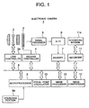
- Fig. 1 is a block diagram showing an electronic camera 1 as an imaging apparatus according to an embodiment of the present invention.
- the electronic camera 1 is equipped with an image-taking lens 2.
- the image-taking lens 2 is controlled by a lens controller 2a upon focusing and stopping down of an aperture stop.
- An imaging surface of a solid-state imaging device 3 is disposed in the image side space of the image-taking lens 2.
- the solid-state imaging device 3 is driven by an instruction of an imaging controller 4 and outputs a signal.
- the signal output from the solid-state imaging device 3 is either an imaging signal or a focal point detection signal. Either way a signal is processed by a signal processor 5 and an A/D converter 6, and stored temporarily in a memory 7.
- the memory 7 is connected to a data bus 8.
- the data bus 8 is connected with the lens controller 2a, the imaging controller 4, a microprocessor 9, a focal point calculator (detection processor) 10, a recorder 11, an image compressor 12, and an image processor 13.
- the microprocessor 9 is connected with an operating portion 9a such as a release button.
- the recorder 11 is removably connected with a recording medium 11a. Movement of the electronic camera 1 is going to be explained later with reference to Fig. 12 .
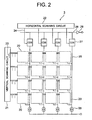
- Fig. 2 is a circuit diagram showing broad configuration of a solid-state imaging device 3 shown in Fig. 1 .
- the solid-state imaging device 3 has a plurality of pixels 20 formed in a grid shape and peripheral circuitry for outputting a signal from the pixel 20.
- the number of pixels is 16 that is four rows horizontally and four columns vertically.
- dotted line denoted by 20 shows an outline of a pixel, specific configuration and circuitry of the pixel are explained later.
- each pixel 20 has the same circuitry and plane structure.
- the pixel 20 outputs either an imaging signal or a focal point detection signal in accordance with a drive signal from peripheral circuitry.
- the whole pixels can be reset their photoelectric converter portions at the same time, so that exposure time and timing thereof can be made the same.
- Peripheral circuitry is composed of a vertical scanning circuit 21, a horizontal scanning circuit 22, drive signal lines 23 and 24 connected thereto, a vertical signal line 25 for receiving signals from pixels, a constant-current power supply 26 for connecting to the vertical signal line 25, a correlation double sampling circuit (CDS) 27, a horizontal signal line 28 for receiving signal output from the correlation double sampling circuit 27, an output amplifier 29, and the like.
- CDS correlation double sampling circuit
- the vertical scanning circuit 21 and the horizontal scanning circuit 22 output a driving signal on the basis of an instruction from the imaging controller 4 of the electronic camera 1.
- Each pixel receives the driving signal output from the vertical scanning circuit 21 through the drive signal line 23, and is driven, and outputs the imaging signal or the focal point detection signal to the vertical signal line 25.
- the vertical scanning circuit 21 outputs a plurality of drive signals. Accordingly, a plurality of drive signal lines 23 are there. This is explained later.
- the signal output from the pixel 20 is carried out predetermined noise reduction by the correlation double sampling circuit 27, and output in accordance with driving signal from the horizontal scanning circuit 22 through the horizontal signal line 28 and the output amplifier 29.
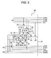
- Fig. 3 is a circuit diagram showing a pixel 20 shown in Fig. 2 .
- the pixel 20 includes four pinned photodiodes 31 through 34 as four photoelectric converter portions for generating and storing electric charge, a first and a second electric charge storage portions 35, 36 for separately storing electric charge transferred from the two pinned photodiodes 32, 33 locating diagonally, a first and a second transfer transistors 37, 38 as a first and a second transfer portions for transferring electric charge from pinned photodiodes 32, 33 to the first and the second electric charge storage portions 35, 36 respectively, a floating diffusion (FD) 40 as a designated portion, a third and a fourth transfer transistors 37, 38 as a third and a fourth transfer gate portions for transferring electric charge from the first and the second electric charge storage portions 35, 36 to the FD40 respectively, an amplifying transistor 43 as an amplifying portion for outputting signal in accordance with the amount of electric charge of FD 40, an FD reset transistor 44 as a first reset portion
- the pixel 20 includes a connection/separation transistor 51 for electrically connecting and separating pinned photodiodes 31 and 32, a connection/separation transistor 52 for electrically connecting and separating pinned photodiodes 33, 34, a connection/separation transistor 53 for electrically connecting and separating pinned photodiodes 31, 33, and a connection/separation transistor 54 for electrically connecting and separating pinned photodiodes 32, 34.
- the first through fourth transfer transistors 37, 38, 41 and 42, the amplifying transistor 43, FD reset transistor 44, the select transistor 45, PD reset transistor 46, connection/separation transistors 51 through 54 are constructed by MOS transistors. In the present embodiment, these transistors except amplifying transistor 43 become on when the gate electrode is high, and off when the gate electrode is low.
- Gate electrodes of connection/separation transistors 51, 52 are mutually connected, and mutually connected to every pixel row, and drive signal (control signal) ⁇ PDB1 is provided from the vertical scanning circuit 21 through drive signal line 23.
- Gate electrodes of connection/separation transistors 53, 54 are mutually connected, and mutually connected to every pixel row, and drive signal (control signal) ⁇ PDB2 is provided from the vertical scanning circuit 21 through drive signal line 23.
- connection/separation transistors 51, 52 become on and connection/separation transistors 53, 54 become off, so that pinned photodiodes 31, 32 are electrically connected, and pinned photodiodes 33, 34 are electrically connected, on the other hand, pinned photodiodes 31, 33 are electrically separated, and pinned photodiodes 32, 34 are electrically separated.
- pinned photodiodes 31 through 34 as a whole become substantially equivalent to an upper-and-lower bisected (bisected into an upper portion and a lower portion) photoelectric converter portion. In the following explanation, this state is called as a PD upper-and-lower bisected state.
- connection/separation transistors 51, 52 become off and connection/separation transistors 53, 54 become on, so that pinned photodiodes 31, 32 are electrically separated, and pinned photodiodes 33, 34 are electrically separated, on the other hand, pinned photodiodes 31, 33 are electrically connected, and pinned photodiodes 32, 34 are electrically connected.
- pinned photodiodes 31 through 34 as a whole become substantially equivalent to a left-and-right bisected (bisected into a left portion and a right portion) photoelectric converter portion. In the following explanation, this state is called as a PD left-and-right bisected state.
- connection/separation transistors 51 through 54 become on, so that pinned photodiodes 31, 32 are electrically connected, pinned photodiodes 33, 34 are electrically connected, pinned photodiodes 31, 33 are electrically connected, and pinned photodiodes 32, 34 are electrically connected.
- pinned photodiodes 31 through 34 as a whole become substantially equivalent to an undivided photoelectric converter portion. In the following explanation, this state is called as a PD undivided state.
- the first and the second electric charge storage portions 35, 36 are provided, and electric charge generated in the pinned photodiodes 31 through 34 is temporarily stored in the first and the second electric charge storage portions 35, 36 before transferring to FD40. Accordingly, it becomes possible to make exposure time and timing thereof regarding the all pixels the same, so that not only synchronism of the image signal can be secured, but also synchronism of the signal upon focal point detection can be secured.
- the present invention is not limited to this, and it may be constructed to carry out rolling shutter without providing electric charge storage portions 35, 36.
- the first transfer transistor 37 transfers electric charge from the pinned photodiode 32 to the first electric charge storage portion 35.
- the place where the electric charge is generated differs under which state the exposure is took place such as the PD upper-and-lower bisected state, the PD left-and-right bisected state, or the PD undivided state.
- the second transfer transistor 38 transfers electric charge from the pinned photodiode 33 to the second electric charge storage portion 36.
- the place where the electric charge is generated also differs under which state the exposure is took place such as the PD upper-and-lower bisected state, the PD left-and-right bisected state, or the PD undivided state.
- Gate electrodes of the first and the second transfer transistors 37, 38 are mutually connected, and mutually connected to every pixel row, and drive signal ⁇ TGA is provided from the vertical scanning circuit 21 through drive signal line 23.
- the first and the second transfer transistors 37, 38 become on at the same time with a given timing in accordance with the drive signal ⁇ TGA, and electric charge is transferred from the two pinned photodiodes 32, 33 to the electric charge storage portions 35, 36 at the same time respectively.
- the present invention is not limited to this, for example, it may be possible to separately provide drive signal to each gate electrode so as to make the first and the second transfer transistor 37, 38 in the on state at the same time.
- the third and the fourth transfer transistors 41, 42 are separately provided drive signals. Gate electrode of the third transfer transistor 41 is mutually connected every pixel row and drive signal ⁇ TGB is provided from the vertical scanning circuit 21 through drive signal line 23. Gate electrode of the fourth transfer transistor 41 is mutually connected every pixel row, and drive signal ⁇ TGC is provided from the vertical scanning circuit 21 through drive signal line 23.
- the third and the fourth transfer transistors 41, 42 become on state with a given timing in accordance with these drive signals ⁇ TGB and ⁇ TGC, and transfer electric charge from the first and the second electric charge storage portions 35, 36 to the FD40 with separate timings or at the same timing.
- Gate electrode of the select transistor 45 is mutually connected every pixel row, and drive signal ⁇ S is provided from the vertical scanning circuit 21 through drive signal line 23.
- Gate electrode of the FD reset transistor 44 is mutually connected every pixel row, and drive signal ⁇ FDR is provided from the vertical scanning circuit 21 through drive signal line 23.
- Gate electrode of the PD reset transistor 46 is mutually connected every pixel row, and drive signal ⁇ PDR is provided from the vertical scanning circuit 21 through drive signal line 23.
- all of the effective pixels have the same structure, and these pixels can output either focal point detection signal or image signal.
- the present invention is not limited to this, and a focal point detection area may be provided to a given position of the solid-state imaging device 3, and pixels for outputting focal point detection signal may be disposed in the area.
- Fig. 3 one terminal of pinned photodiodes 31 through 34, one terminal of electric charge storage portions 35, 36, and one terminal of the FD40 are expediently shown to be grounded. However, as will be understood from Figs. 5 through 8 explained later, they become electric potentials of P-well 62.
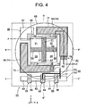
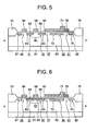
- Fig. 4 is a plan view typically showing the pixel shown in Fig. 2 .
- Figs. 5 and 6 are sectional views along A-A' line in Fig. 4 .
- Fig. 5 shows a state where the second gate electrode is low (in other words, ⁇ PDB2 is low), and the connection/separation transistor 51 is made to be off.
- Fig. 7 is a sectional view along B-B' line in Fig. 4 .
- Fig. 8 is a sectional view along C-C' line in Fig. 4 .
- the micro-lens is omitted.
- drive lines are omitted, except electrical connection of lines in the pixel 20.
- X direction is the right-and-left direction
- +X direction is the right side
- -X direction is the left side
- Y direction is the upper-and-lower direction
- +Y direction is the upper side
- -Y direction is the lower side.
- a P-type well 62 is formed on an N-type silicon substrate 61.
- An N-type charge storage layer 63 is formed on the P-type well 62, and by adding a P-type depletion prevention layer 64 on the surface side of the charge storage layer 63 pinned photodiodes 31 through 34 are composed.
- the construction of a pinned photodiode is adopted, the present invention is not limited to this, and the depletion prevention layer may be omitted.
- the four pinned photodiodes 31 through 34 are disposed in four areas divided by a division line B-B' in Y direction and a division line D-D' in X direction each crossing in a plane seen from Z direction.
- the pinned photodiode 31 is disposed in the upper left area
- the pinned photodiode 32 is in the upper right area
- the pinned photodiode 33 is in the lower left area
- the pinned photodiode 34 is in the lower right area among the four areas.
- These pinned photodiodes 31 through 34 are disposed near to the intersection of the division lines B-B' and D-D', and disposed rotationally symmetric around the intersection. As shown in Fig.
- a micro-lens 65 for leading incident light to the pinned photodiodes 31 through 34 is disposed.
- the micro-lens is disposed such that the centerline thereof passes through the intersection of the division lines B-B' and D-D'. Accordingly, incident light led by the micro-lens 65 is divided at the pupil and led to each pinned photodiodes 31 through 34.
- the micro-lens may be disposed such that in a pixel located near the center of the effective pixel area the center of the micro-lens comes to the intersection of the division lines B-B' and D-D', on the other hand, in the periphery of the effective pixel area the center of the micro-lens comes to a shifted position from the intersection.
- the first gate electrode 67 is disposed along the division line B-B', and the second gate electrode 68 is disposed along the division line D-D'.
- the second gate electrode 68 is formed on between the pinned photodiodes 31 and 32, and between the pinned photodiodes 33 and 34 through a thin silicon oxide layer 66.
- the second gate electrode 68 forms a gate of an MOS transistor (connection/separation transistor 51) composed of the charge storage layer 63 of the pinned photodiode 31 and the charge storage layer 63 of the pinned photodiode 32 as a source or a drain, and a gate of an MOS transistor (connection/separation transistor 52) composed of the charge storage layer 63 of the pinned photodiode 33 and the charge storage layer 63 of the pinned photodiode 34 as a source or a drain.
- the drive signal ⁇ PDB1 is provided to the second gate electrode 68 from a line (not shown).
- the first gate electrode 67 is formed on between the pinned photodiodes 31 and 33, and between the pinned photodiodes 32 and 34 through a thin silicon oxide layer 66. Accordingly, the first gate electrode 67 forms a gate of an MOS transistor (connection/separation transistor 53) composed of the charge storage layer 63 of the pinned photodiode 31 and the charge storage layer 63 of the pinned photodiode 33 as a source or a drain, and a gate of an MOS transistor (connection/separation transistor 54) composed of the charge storage layer 63 of the pinned photodiode 32 and the charge storage layer 63 of the pinned photodiode 34 as a source or a drain.
- the drive signal ⁇ PDB2 is provided to the first gate electrode 68 from a line (not shown).
- the gate electrode of the second gate electrode 68 passes over the gate electrode 67 through an insulation layer as shown in Fig. 7 .
- connection/separation transistor 51 when the second gate electrode 68 is low ( ⁇ PDB2 is low), since an inversion layer does not generated in the channel area of the connection/separation transistor 51 as shown in Fig. 5 , the connection/separation transistor 51 becomes off. On the other hand, when the second gate electrode 68 is high ( ⁇ PDB2 is high), since an inversion layer 69 is generated in the channel area of the connection/separation transistor 51, the connection/separation transistor 51 becomes on. The similar can be applied to the other connection/separation transistors 52 through 54.
- connection/separation transistors 51 through 54 become off when the voltage of the gate thereof is made to become zero potential (voltage of the substrate 1), they may be made to be on when the difference to the zero potential becomes large. Moreover, although the connection/separation transistors 51 through 54 become on when the voltage of the gate thereof is made to become zero potential (voltage of the substrate 1), they may be made to be off when negative voltage than the zero potential is applied. When the connection/separation transistors 51 through 54 are constructed to be off when the gate voltage is not applied, they become on when the positive voltage applied to the gate voltage, and when the connection/separation transistors 51 through 54 are constructed to be on when the gate voltage is not applied, they become off when the negative voltage is applied to the gate voltage.
- the first and the second gate electrodes 67, 68 are made from a transparent material such as an ITO film. Accordingly, incident light is not blocked by the first and the second gate electrodes 67, 68, and reaches the area between the pinned photodiodes 31 through 34 located under the first and the second gate electrodes 67, 68. Accordingly, for example, when the connection/separation transistor 51 is on as shown in Fig. 6 , since an inversion layer 69 formed between the pinned photodiodes 31 and 32 has a photoelectric conversion function, using efficiency of the incident light can be enhanced. On the other hand, when the connection/separation transistor 51 is off as shown in Fig.
- the first and the second gate electrodes 67, 68 may be constructed by polysilicon instead of the ITO film.
- polysilicon although transmittance becomes partly lower than that of ITO film, since it can easily be formed as a fine structure, from collective consideration, there are instances where polysilicon can further reduce amount of light loss.
- the first and the second gate electrodes 67, 68 may be constructed by a light blocking material.
- the first and the second gate electrodes 67, 68 form a mode setting means capable of selectively setting mode such as a PD upper-and-lower bisected state (a first mode), a PD left-and-right bisected state (a second mode), and a PD undivided state (a third mode) in accordance with control signals ( ⁇ PDB2 and ⁇ PDB1).
- a PD upper-and-lower bisected state signals of pinned photodiodes 31, 32 are added, and signals of pinned photodiodes 33, 34 are added, and these added signals are independently obtained.
- signals of pinned photodiodes 31, 33 are added, and signals of pinned photodiodes 32, 34 are added, and these added signals are independently obtained.
- signals of pinned photodiodes 31 through 34 are added.
- pinned photodiodes 31 through 34 are constructed to be completely electrically separated with each other, by suitably disposing charge storage portions and transfer switches so as to independently use or add signals red out from pinned photodiodes 31 through 34 in accordance with control signal, it becomes possible to realize the similar signal adding modes such as the PD left-and-right bisected state, the PD left-and-right bisected state, and the PD undivided state, so that the present invention may include such construction.
- the present invention may include such construction.
- the number of external charge storage portions and transfer switches can be reduced and wiring can be simplified, so that it is much desirable.
- gate electrodes 71, 72 are respectively formed through a thin silicon oxide film 66.
- the first and a second transfer transistors 37, 38 are constructed as MOS transistors whose gates are gate electrodes 71, 72, and whose source and drain are electric charge storage potions 35, 36 and pinned photodiodes 32, 33, respectively.
- the gate electrodes 71, 72 are connected each other with a line not shown. Accordingly, the first and the second transfer transistors 37, 38 are on and off at the same time in accordance with drive signal ⁇ TGA. Therefore, respective electric charges from pinned photodiodes 32, 33 are transferred to corresponding electric charge storage portions 35, 36 at the same time.
- the electric charge storage portions 35, 36 include N-type layers 73, 74 formed on the P-type well 62.
- the gate electrodes 71, 72 of the first and the second transfer transistor 37, 38 are disposed over upper parts of the two N-type layers 73, 74. In this manner, the electric charge storage portions 35, 36 are constructed as MOS capacitors by the gate electrodes 71, 72 and the N-type layers 73, 74.
- FD40 is constructed as substantially one floating diffusion by electrically connecting two N-type areas 75, 76 formed separately on the P-type well with a wiring 77. Electric charge is transferred from either of the two electrical charge storage portions 35 and 36 to the FD40.
- Gate electrodes 78, 79 are formed through a thin silicon oxide film 66 between the first and the second electric charge storage portions 35, 36 and N-type diffusion layer as the FD40.
- the third and the fourth transfer transistors 41, 42 are constructed as MOS transistors making the gate electrodes 78, 79 as gates, and N-type layers 71, 72 of the electric charge storage portions 35, 36 and N-type diffusion area of the FD40 as sources or drains.
- the gate electrode 78 of the third transfer transistor 41 and the gate electrode 79 of the fourth transfer transistor 42 are independently formed and supplied with independent drive signals ⁇ TGB and ⁇ TGC from the vertical scanning circuit 21. Accordingly, the third and the fourth transfer transistors 41, 42 are independently driven in accordance with respective drive signals ⁇ TGB and ⁇ TGC. Therefore, the third and the fourth transfer transistors 41, 42 can transfer electric charge from the first and the second electric charge storage portions 35, 36 either at the same time or different timings to the FD40.
- N-type diffusion layers 81 through 83 are formed along C-C' line in Fig. 4 .
- the N-type layer 81 is connected to a power supply VDD by unillustrated wiring.
- a gate electrode 84 is formed on the N-type layers 81, 82 through a thin silicon oxide film 66.
- the amplifying transistor 43 is constructed as an MOS transistor making the gate electrode 84 as a gate, and the N-type layers 81, 82 as a source or a drain.
- the gate electrode 84 is connected to the FD40 (N-type layers 75, 76) by the wiring 77.
- a gate electrode 85 is formed on a space between N-type layers 82 and 83 through a thin silicon oxide film 66.
- the select transistor 45 is constructed as an MOS transistor making the gate electrode 85 as a gate, and N-type layers 82, 83 as a source or a drain.
- a gate electrode 86 is formed on a space between N-type layers 76 and 81 through a thin silicon oxide film 66.
- the FD reset transistor 44 is constructed as an MOS transistor making the gate electrode 86 as a gate, and N-type layers 76, 81 as a source or a drain.
- N-type layer 87 is formed in P well 62.
- a gate electrode 88 is formed on a space between N-type layer 87 and the pinned photodiode 31 through a thin silicon oxide film 66.
- PD reset transistor 46 is constructed as an MOS transistor making the gate electrode 88 as a gate, and N-type layer 87 and the electric charge storage layer 63 of the pinned photodiode 31 as a source or a drain.
- Drive signal ⁇ PDR is supplied to the gate electrode 88 by an unillustrated wiring.
- a second reset portion (here, PD reset transistor 46) discharges unnecessary electric charge in the pinned photodiodes 31 through 34.
- unnecessary electric charge there are reset electric charge upon operating electric shutter and overflowed electric charge upon receiving strong incident light.
- unnecessary electric charge may be transferred to the FD40 and discharged by the first reset portion (here, FD reset transistor 44).
- the second reset portion is not necessary to be disposed.
- thick silicon oxide film 70 is formed on the circumference of the pinned photodiodes 31 through 34 and each N-type layer, and each element is separated.
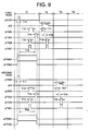
- Fig. 9 is a timing chart showing drive signals (in other words, drive signals for reading out signals from pixels exposed in a PD undivided state) for reading out imaging signal.
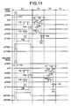
- Fig. 10 is a timing chart showing drive signals for reading out focal point detection signal from pixels exposed in a PD left-and-right bisected state.
- Fig. 11 is a timing chart showing drive signals for reading out focal point detection signal from pixels exposed in a PD upper-and-lower bisected state.
- a signal line is selected every one horizontal row, and moved successively to the next row.
- movement shown in Figs. 9 through 11 is carried out, and drive signals shown in figures are output.
- the scanning is repeated over entire image field in vertical direction.
- select movement is returned to the top row after a vertical returning period has elapsed.
- Figs. 9 through 11 only shows drive signals in the first and the second rows.
- a period T1 is a period when all effective pixels are driven at the same time.
- the same drive signals are output in all rows.
- the period T2 is a period for reading out the first row
- the period T3 is a period for reading out the second row
- the period T4 is a period for reading out the third row
- the drive signal shown in the figure is output only to the selected row. The same holds for Figs. 10 and 11 explained later.
- ⁇ PDR is made high, so that the PD reset transistor 46 becomes on.
- unnecessary electric charge stored in all effective pixels in the pinned photodiodes 31 through 34 is discharged to the electric power supply VDD.
- the pinned photodiodes 31 through 34 are reset.
- the pinned photodiodes 31 through 34 in all effective pixels start exposure at the time the period T11 is finished.
- photoelectric conversion of incident light is performed in the area of the pinned photodiodes 31 through 34 as described above.
- ⁇ TGA is made high, so that the first and the second transfer transistors 37, 38 become on. All electric charge stored in the connected pinned photodiodes 31 through 34 and spaces between them in all effective pixels are transferred to the first and the second electric charge storage portions 35, 36 separately.
- the period T15 (the period from the time ⁇ PDR is made low to the time ⁇ TGA is made on) shown in Fig. 9 becomes exposure time. Exposure time T15 is the same period and the same timing for all effective pixels. Accordingly, all effective pixels can obtain imaging information without making mistakes in the timing.
- ⁇ S in the first row is made high, so that the selection transistor 45 becomes on. Accordingly, pixels in the first row are selected, and signals from the pixels in the first row are output to the vertical signal line 25.
- the second row is red out.
- the drive signal is the same as the first row.
- the periods T26 through T29 in Fig. 9 are corresponding to the periods T16 through T19.
- ⁇ PDR may be always high after completion of reading out (after ⁇ S is off).
- each pixel makes ⁇ PDB1, ⁇ PDB2 high, and combines four pinned photodiodes 31 through 34 in the period from the start of the period T11 to the end of the period T14, image signal can be output as usual.
- gate electrodes 67, 68 disposed along the division lines B-B', D-D' transmits incident light, using efficiency of the incident light enhances and sensitivity can be improved.
- an electronic shutter capable of making exposure timing of all pixels the same is possible. There is no doubt that the movement of a rolling shutter for resetting every row is also possible.
- This movement is carried out when desired row of pixels standing in a line in the left-and-right direction are used as a focal point detection line sensor to obtain focal point detection signal.
- a left-half signal in the present embodiment, the signal photoelectrically converted from the area between pinned photodiodes 31 and 33 is added
- a right-half signal in the present embodiment, the signal photoelectrically converted from the area between pinned photodiodes 32 and 34 is added
- the signal of all pixels red out in this manner is temporally stored in the memory 7 shown in Fig.
- focal point detection processing upon carrying out focal point detection processing at the focal point calculator, signals regarding only desired row of pixels are selectively used from the memory 7.
- focal point detection signal is obtained by reading out all pixels, pixels other than desired row of pixels may be thinned out and not necessary to be red out.
- ⁇ PDR is made to be high, so that PD reset transistor 46 becomes on, and ⁇ PDB1 and ⁇ PDB2 are made to be high, so that it becomes PD undivided state.
- unnecessary electric charge stored in pinned photodiodes 31 through 34 of all effective pixels is discharged to the power supply VDD.
- the pinned photodiodes 31 through 34 are reset.
- the pinned photodiodes 31 through 34 of all effective pixels starts exposure at the end of the period T31.
- photoelectric conversion of the incident light is carried out even on the area between the pinned photodiodes 31 through 34 as described above.
- ⁇ PDB1 is made to be low after termination of the period T31, even after terminating the period T31 ⁇ PDB2 is kept high until termination of the period T34. Accordingly, in the period after termination of the period T31 until termination of the period T34 all effective pixels become the PD left-and-right bisected state and the pinned photodiodes 31 through 34 of each pixel as a whole become substantially equivalent to a left-and-right bisected (bisected to a left portion and a right portion) photoelectric converter portion. In this period, movements according to the period T32 through T34 explained below are carried out.
- ⁇ FDR is made to be high, so that the FD reset transistor 44 becomes on.
- ⁇ TGB and ⁇ TGC are made to be high, so that the third and the fourth transfer transistor 41, 42 become on at the same time.
- the period T34 (the period from making ⁇ PDR low to making ⁇ TGA on) shown in Fig. 10 is the exposure period.
- the exposure period T35 is the same period and the same timing for all effective pixels. Accordingly, all effective pixels can obtain focal point detection information without shifting timing.
- the movements of the period so far (period T1) is the same as the movements for obtaining image signal explained with reference to Fig. 9 except exposure is carried out in the PD left-and-right bisected state.
- ⁇ S of the first row is made to be high, so that the select transistor 45 becomes on. Accordingly, pixels of the first row are selected, and signals are output from pixels of the first row to the vertical signal line 25.
- ⁇ FDR of the first row is made to be high, and the FD reset transistor 44 is on. With this movement, FD40 is reset.
- the output from the amplifying transistor 43 of the first row upon resetting the FD40 is stored in the CDS circuit 27 through the vertical signal line 25.
- ⁇ TGC is made to be high, so that the fourth transfer transistor 42 becomes on. Accordingly, electric charge stored in the second electric charge storage portion 36 is transferred to the FD40. Potential amplified in accordance with the amount of electric charge is transferred to the CDS circuit 27 through the vertical signal line 25. In the CDS circuit 27, the difference from the previously stored output upon resetting is output as a pupil signal output of the other of the left-and-right direction of the pixels in the first row. These pupil signal output of the other of the left-and-right direction of the pixels in the first row is output by the drive signal of the horizontal scanning circuit 22 through the horizontal signal line 28 and the output amplifier 29.
- pupil signal output of one of the left-and-right direction and pupil signal output of the other of the left-and-right direction of the pixels in the first row can be obtained.
- ⁇ PDR After completion of readout (after ⁇ S is off) ⁇ PDR may be always high.
- ⁇ PDR may be always high.
- each pixel becomes in the PD left-and-right bisected state by making ⁇ PDB1 low and making ⁇ PDB2 high in the period from the completion of the period T31 to the completion of the period T34, pupil signal output of one side in the left-and-right direction and pupil signal output of the other side in the left-and-right direction of each pixel can be obtained.
- gate electrodes 67, 68 disposed along the division lines B-B', D-D' transmit incident light, using efficiency of the incident light increases, and sensitivity of the focal point detection signal can be increased.
- an electronic shutter upon obtaining focal point detection signal, an electronic shutter whose exposure timing is the same over entire effective pixels can be available.
- This movement is carried out when desired column of pixels standing in a line in the upper-and-lower direction are used as a focal point detection line sensor to obtain focal point detection signal.
- an upper-half signal in the present embodiment, the signal photoelectrically converted from the area between pinned photodiodes 31 and 32 is added
- a lower-half signal in the present embodiment, the signal photoelectrically converted from the area between pinned photodiodes 33 and 34 is added
- the signal of all pixels red out in this manner is temporally stored in the memory 7 shown in Fig.
- focal point detection signal is obtained by reading out all pixels, pixels other than desired column of pixels are not necessary to be red out, or may be thinned out.
- the movement shown in Fig. 11 is basically similar to the afore-mentioned movement shown in Fig. 10 .
- the point of difference is that ⁇ PDB1 is interchanged with ⁇ PDB2.
- ⁇ PDB1 is on in the period from the start of the period T31 to the end of the period T34, and ⁇ PDB2 is on only in the period T31.
- focal point detection signal (pupil signal output of one side in the left-and-right direction and pupil signal output of the other side in the left-and-right direction) for detecting phase shift in the left-and-right direction can be obtained from any desired pixel line standing in line left-and-right direction.
- focal point detection signal for detecting phase shift in the left-and-right direction
- focal point detection signal (pupil signal output of one side in the upper-and-lower direction and pupil signal output of the other side in the upper-and-lower direction) for detecting phase shift in the upper-and-lower direction can be obtained from any desired pixel line standing in line upper-and-lower direction.
- the aforementioned solid-state imaging device 3 does not cause an effect something like a defect pixel, but is able to freely change whether which pixel functions as a pixel having a photoelectric converter portion bisected in which direction, so that it becomes possible to obtain an advantage that accuracy of focal point detection can be increased.
- a pupil division phase difference detection method in order to detect focal point at the center, upper part, or lower part of the image frame, it is said to be necessary to dispose left-and-right bisected photodiodes in the vertical direction (upper-and-lower direction) in a line sensor shape, and in order to detect focal point at the center, left part, or right part of the image frame, it is said to be necessary to dispose upper-and-lower bisected photodiodes in the horizontal direction (left-and-right direction) in a line sensor shape.
- the aforementioned solid-state imaging device 3 can carry out focal point detection in the horizontal direction (left-and-right direction) as well as in the vertical direction (upper-and-lower direction) despite of the same pixel configuration.
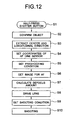
- Step S1 When a release button in the operating portion 9a is half-pressed (Step S1), the microprocessor 9 in the electronic camera 1 drives the imaging controller 4 corresponding to the half-press operation.
- the imaging controller 4 reads out imaging signal for confirming object from all pixels or given pixels by a given well-known method, and stores in the memory 7. In this case, when all pixels are to be red out, for example, the same movements shown in Fig. 9 are carried out.
- the image processor confirms object by using image confirming technique from the signal (Step S2). For example, in a face confirming mode, a face as an object is confirmed.
- the image processor 13 picks up central coordinates and a longitudinal direction of the object (Step S3).
- the microprocessor 9 sets coordinates of pixel line (position and longitudinal direction) corresponding to a line sensor for auto focus optimum for precision detection of focusing state to the object on the basis of the center coordinates and longitudinal direction picked up in step S3 (Step S4).
- Microprocessor 9 sets shooting condition (aperture stop, focusing state, shutter speed, and the like) for focal point detection on the basis of confirmation results in step S2 (Step S5).
- the microprocessor 9 successively moves the lens controller 2a to become the conditions such as aperture stop set by the step S5, and drives the imaging controller 4 to become shutter speed condition set by the step S5 and pixel line coordinates set by the step S4, and reads out auto focus signal to store the memory 7 (Step S6).
- the pixel line set in the step S4 is a pixel line standing in line of left-and-right direction
- image signal for auto focus is red out by the movements shown in Fig. 10 .
- the pixel line set in the step S4 is a pixel line standing in line of upper-and-lower direction
- image signal for auto focus is red out by the movements shown in Fig. 11 .
- the microprocessor 9 picks up signals of each pixel in the pixel line of coordinates set in the step S4 among signals of all pixels stored in the memory 7 obtained in the step S6, makes the focal point calculator 10 calculate in accordance with the pupil division phase difference detection method on the basis of these signals to obtain an amount of defocus (Step S7).
- the microprocessor 9 makes the lens controller 2a adjust the image-taking lens 2 to come to focus state in accordance with the amount of defocus calculated in step S7.
- the microprocessor 9 successively set shooting condition (aperture stop, shutter speed, and the like) for shooting.
- the microprocessor 9 makes the lens controller 2a set the aperture stop an the like to become the condition set in the step S9, and in synchronization with a full-press of the release button in the operating portion 9a drives the imaging controller 4 with the shutter time condition, and the like set in the step S9, so that shooting is carried out by reading out image signal (Step S10).
- image signal is red out by the aforementioned movement shown in Fig. 9 .
- the image signal is stored in the memory 7 by the imaging controller 4.
- the microprocessor 9 if required, performs required processing in the image processor 13 or the image compressor 12 on the basis of an instruction of the operating portion 9a, and makes the recorder output the processed signal to store in the recording medium 11a.
- CMOS type image sensor various kinds of pixel structure have been known.
- the present invention can apply to those image sensors.
- the present invention can apply to various image sensors other than the CMOS type image sensor.
- connection/separation transistors 51 through 54 are MOS transistors, those may be, for example, junction-field-effect-transistors (J-FET).
Landscapes
- Engineering & Computer Science (AREA)
- Multimedia (AREA)
- Signal Processing (AREA)
- Solid State Image Pick-Up Elements (AREA)
- Transforming Light Signals Into Electric Signals (AREA)
Claims (9)
- Festkörper-Bildgebungsvorrichtung (3) für das photoelektrische Konvertieren eines Objektbilds, das durch eine bildaufnehmende Linse (2) gebildet wird, umfassend eine Vielzahl an Pixeln (20), die zweidimensional angeordnet sind,
mindestens ein Pixel (20) unter der Vielzahl an Pixeln (20) umfassend vier photoelektrische Konvertierungsabschnitte (31-34), von denen sich jeder in einem von vier Bereichen befindet, die durch eine erste Linie geteilt sind, die sich in eine erste Richtung erstreckt, und eine zweite Linie, die sich in eine zweite Richtung erstreckt, wobei sich die erste und zweite Linie in einer Draufsicht kreuzen und eine photoelektrische Konvertierung ausführen, und ein Moduseinstellmittel (67, 68), das in der Lage ist, jeden von einem ersten bis zu einem dritten Modus selektiv gemäß einem Steuerungssignal durch elektrisches Verbinden und Trennen von zwei der photoelektrischen Konvertierungsabschnitte, die durch die erste und zweite Linie getrennt sind, einzustellen;
wobei der erste Modus ein Modus ist, in dem zwei photoelektrische Konvertierungsabschnitte, die sich in einer Seite der ersten Linie unter den vier photoelektrischen Konvertierungsabschnitten (31-34) befinden, elektrisch verbunden sind, so dass zwei photoelektrische Konvertierungsabschnitte, die sich in der anderen Seite der ersten Linie unter den vier photoelektrischen Konvertierungsabschnitten (31-34) befinden, elektrisch verbunden sind, und dass die photoelektrischen Konvertierungsabschnitte, die sich in Bezug auf die erste Linie unter den vier photoelektrischen Konvertierungsabschnitten (31-34) auf einer anderen Seite befinden, elektrisch getrennt sind;
wobei der zweite Modus ein Modus ist, in dem zwei photoelektrische Konvertierungsabschnitte, die sich in einer Seite der zweiten Linie unter den vier photoelektrischen Konvertierungsabschnitten (31-34) befinden, elektrisch verbunden sind, so dass zwei photoelektrische Konvertierungsabschnitte, die sich in der anderen Seite der zweiten Linie unter den vier photoelektrischen Konvertierungsabschnitten (31-34) befinden, elektrisch verbunden sind, und so dass die photoelektrischen Konvertierungsabschnitte, die sich in Bezug auf die zweite Linie unter den vier photoelektrischen Konvertierungsabschnitten (31-34) auf einer anderen Seite befinden, elektrisch getrennt sind;
wobei der dritte Modus ein Modus ist, in dem zwei photoelektrische Konvertierungsabschnitte, die sich in einer Seite der ersten Linie unter den vier photoelektrischen Konvertierungsabschnitten (31-34) befinden, elektrisch miteinander verbunden sind, so dass zwei photoelektrische Konvertierungsabschnitte, die sich in der anderen Seite der ersten Linie unter den vier photoelektrischen Konvertierungsabschnitten (31-34) befinden, elektrisch miteinander verbunden sind, so dass zwei photoelektrische Konvertierungsabschnitte, die sich in einer Seite der zweiten Linie unter den vier photoelektrischen Konvertierungsabschnitten (31-34) befinden, elektrisch miteinander verbunden sind, und dass zwei photoelektrische Konvertierungsabschnitte, die sich in der anderen Seite der zweiten Linie unter den vier photoelektrischen Konvertierungsabschnitten (31-34) befinden, elektrisch miteinander verbunden sind;
dadurch gekennzeichnet, dass
das Moduseinstellmittel (67, 68) eine erste Gate-Elektrode (67) umfasst, die entlang der ersten Linie angeordnet ist, und eine zweite Gate-Elektrode (68), die entlang der zweiten Linie angeordnet ist, wobei die erste (67) und zweite Gate-Elektrode (68) aus einem transparenten Material hergestellt sind, und
wobei jeder Bereich der Festkörper-Bildgebungsvorrichtung (3), der sich zwischen zwei benachbarten photoelektrischen Konvertierungsabschnitten befindet, wobei sich die erste oder die zweite Linie dazwischen befindet, als ein photoelektrischer Konvertierer funktioniert, wenn die benachbarten zwei elektrischen Konvertierungsabschnitte elektrisch verbunden sind, und nicht als photoelektrischer Konvertierer funktioniert, wenn die benachbarten zwei photoelektrische Konvertierungsabschnitte elektrisch getrennt sind. - Festkörper-Bildgebungsvorrichtung (3) nach Anspruch 1, wobei jeder des mindestens einen Pixels (20) darauf mit einer Mikrolinse (65) vorgesehen ist, um Licht in die vier photoelektrischen Konvertierungsabschnitte (31-34) zu leiten.
- Festkörper-Bildgebungsvorrichtung (3) nach Anspruch 1 oder 2, wobei die erste Gate-Elektrode (67) ein Gate eines MOS-Transistors bildet, der Halbleiterbereiche der zwei photoelektrischen Konvertierungsabschnitte, die sich auf einer Seite der zweiten Linie unter den vier photoelektrischen Konvertierungsabschnitten (31-34) befinden, als Quelle (Source) oder Drain (Abfluss) einrichtet, und ein Gate eines MOS-Transistors, der Halbleiterbereiche der zwei photoelektrischen Konvertierungsabschnitte, die sich auf der anderen Seite der zweiten Linie unter den vier photoelektrischen Konvertierungsabschnitten (31-34) befinden, als Quelle (Source) oder Drain (Abfluss) einrichtet, und
die zweite Gate-Elektrode (68) ein Gate eines MOS-Transistors bildet, der Halbleiterbereiche der zwei photoelektrischen Konvertierungsabschnitte, die sich auf einer Seite der ersten Linie unter den vier photoelektrischen Konvertierungsabschnitten (31-34) befinden, als Quelle (Source) oder Drain (Abfluss) einrichtet, und ein Gate eines MOS-Transistors, der Halbleiterbereiche der zwei photoelektrischen Konvertierungsabschnitte, die sich auf der anderen Seite der ersten Linie unter den vier photoelektrischen Konvertierungsabschnitten (31-34) befinden, als Quelle (Source) oder Drain (Abfluss) einrichtet. - Festkörper-Bildgebungsvorrichtung (3) nach Anspruch 1, 2 oder 3, wobei die erste und zweite Gate-Elektrode (67, 68) aus Polysilizium hergestellt sind.
- Festkörper-Bildgebungsvorrichtung (3) nach einem der Ansprüche 1 bis 4, wobei jedes des mindestens einen Pixels (20) Folgendes umfasst:einen ersten und einen zweiten elektrischen Ladungsspeicherabschnitt (35, 36) jeweils zum Speichern elektrischer Ladung, die von zwei photoelektrischen Konvertierungsabschnitten transferiert wird, die sich unter den vier photoelektrischen Konvertierungsabschnitten (31-34) diagonal voneinander befinden,einen Ladungsakkumulierungsabschnitt (40), der selektiv elektrische Ladung von einem ersten und zweiten Speicherabschnitt empfängt,ein Verstärker (43) zum Ausgeben des Signals entsprechend einer elektrischen Ladungsmenge des Ladungsakkumulierungsabschnitts (40),ein erstes Transfer-Gate (37) zum Transferieren elektrischer Ladung von einem der zwei diagonal von einander befindlichen photoelektrischen Konvertierungsabschnitte zum ersten elektrischen Ladungsspeicherabschnitt (35),ein zweites Transfer-Gate (38) zum Transferieren elektrischer Ladung vom anderen der zwei diagonal von einander befindlichen photoelektrischen Konvertierungsabschnitte zum zweiten elektrischen Ladungsspeicherabschnitt (36),ein drittes Transfer-Gate (41) zum Transferieren elektrischer Ladung vom ersten elektrischen Ladungsspeicherabschnitt (36) zum Ladungsakkumulierungsabschnitt (40), undein viertes Transfer-Gate (42) zum Transferieren elektrischer Ladung vom zweiten elektrischen Ladungsspeicherabschnitt (36) zum Ladungsakkumulierungsabschnitt (40).
- Festkörper-Bildgebungsvorrichtung (3) nach Anspruch 5, wobei jedes des mindestens einen Pixels ein Entladungs-Gate (46) für elektrische Ladung zum Endladen elektrischer Ladung von mindestens einem photoelektrischen Konvertierungsabschnitt der vier photoelektrischen Konvertierungsabschnitte (31-34) umfasst.
- Eine Bildgebungseinrichtung (1) umfassend eine Bildaufnahmelinse (2), die Festkörper-Bildgebungsvorrichtung (3) nach einem der Ansprüche 1 bis 6 und einen Signalprozessor (5) zum Ausgeben eines Detektionssignals, das den Fokussierungszustand der Bildaufnahmelinse (2) auf Basis der Signale ausgibt, die im ersten Modus oder im zweiten Modus von jedem ausgewählten Pixel (20) des mindestens einen Pixels (20) bezogen werden.
- Bildgebungseinrichtung (1) nach Anspruch 7, wobei gemäß dem Objektbild bestimmt wird, auf welchem Modus unter dem ersten und dem zweiten Modus die Detektion des Fokuseinstellungszustands der Bildaufnahmelinse (2) basiert.
- Bildgebungseinrichtung (1) nach Anspruch 7, wobei eine Linsensteuereinheit (2a) zum Steuern der Fokuseinstellung der Bildaufnahmelinse (2) auf Basis des Detektionssignals vom Signalprozessor (10) enthalten ist.
Applications Claiming Priority (2)
| Application Number | Priority Date | Filing Date | Title |
|---|---|---|---|
| JP2006155496A JP4835270B2 (ja) | 2006-06-03 | 2006-06-03 | 固体撮像素子及びこれを用いた撮像装置 |
| PCT/JP2007/061251 WO2007142171A1 (ja) | 2006-06-03 | 2007-05-29 | 固体撮像素子及びこれを用いた撮像装置 |
Publications (3)
| Publication Number | Publication Date |
|---|---|
| EP2037672A1 EP2037672A1 (de) | 2009-03-18 |
| EP2037672A4 EP2037672A4 (de) | 2010-07-28 |
| EP2037672B1 true EP2037672B1 (de) | 2014-08-06 |
Family
ID=38801422
Family Applications (1)
| Application Number | Title | Priority Date | Filing Date |
|---|---|---|---|
| EP07744636.7A Ceased EP2037672B1 (de) | 2006-06-03 | 2007-05-29 | Festkörper-bildgebungselement und bildgebungseinrichtung damit |
Country Status (5)
| Country | Link |
|---|---|
| US (1) | US8159580B2 (de) |
| EP (1) | EP2037672B1 (de) |
| JP (1) | JP4835270B2 (de) |
| CN (1) | CN101461230B (de) |
| WO (1) | WO2007142171A1 (de) |
Families Citing this family (47)
| Publication number | Priority date | Publication date | Assignee | Title |
|---|---|---|---|---|
| US7755121B2 (en) | 2007-08-23 | 2010-07-13 | Aptina Imaging Corp. | Imagers, apparatuses and systems utilizing pixels with improved optical resolution and methods of operating the same |
| US7495228B1 (en) * | 2008-03-31 | 2009-02-24 | General Electric Company | Dual function detector device |
| JP5568880B2 (ja) * | 2008-04-03 | 2014-08-13 | ソニー株式会社 | 固体撮像装置、固体撮像装置の駆動方法および電子機器 |
| JP5328224B2 (ja) * | 2008-05-01 | 2013-10-30 | キヤノン株式会社 | 固体撮像装置 |
| EP2445008B1 (de) * | 2008-08-11 | 2015-03-04 | Honda Motor Co., Ltd. | Abbildungsvorrichtung und Bilderzeugungsverfahren |
| JP5461343B2 (ja) * | 2010-08-24 | 2014-04-02 | 富士フイルム株式会社 | 撮像素子及び撮像装置 |
| JP2012105023A (ja) | 2010-11-09 | 2012-05-31 | Canon Inc | 画像処理装置、撮像装置、及び画像処理方法 |
| JP5456644B2 (ja) * | 2010-11-17 | 2014-04-02 | 本田技研工業株式会社 | 受光素子及び制御方法 |
| JP5627438B2 (ja) | 2010-12-14 | 2014-11-19 | キヤノン株式会社 | 撮像装置、その制御方法、プログラム及び記憶媒体 |
| JP5778931B2 (ja) | 2011-01-25 | 2015-09-16 | キヤノン株式会社 | 撮像装置及びその制御方法 |
| JP5856376B2 (ja) | 2011-01-27 | 2016-02-09 | キヤノン株式会社 | 撮像装置及びその制御方法 |
| JP5785398B2 (ja) * | 2011-02-17 | 2015-09-30 | キヤノン株式会社 | 撮像装置及び画像信号処理装置 |
| JP5954964B2 (ja) * | 2011-02-18 | 2016-07-20 | キヤノン株式会社 | 撮像装置およびその制御方法 |
| JP6041495B2 (ja) * | 2011-03-24 | 2016-12-07 | キヤノン株式会社 | 撮像装置及び欠陥画素の判定方法 |
| JP6039165B2 (ja) | 2011-08-11 | 2016-12-07 | キヤノン株式会社 | 撮像素子及び撮像装置 |
| US20140191290A1 (en) * | 2011-08-24 | 2014-07-10 | Sharp Kabushiki Kaisha | Solid-state imaging element |
| FR2979485B1 (fr) * | 2011-08-26 | 2016-09-09 | E2V Semiconductors | Capteur d'image a regroupement de pixels |
| JP5850680B2 (ja) * | 2011-09-09 | 2016-02-03 | キヤノン株式会社 | 撮像装置及びその制御方法 |
| US8710420B2 (en) * | 2011-11-08 | 2014-04-29 | Aptina Imaging Corporation | Image sensor pixels with junction gate photodiodes |
| JP5967944B2 (ja) | 2012-01-18 | 2016-08-10 | キヤノン株式会社 | 固体撮像装置およびカメラ |
| JP6172888B2 (ja) * | 2012-01-18 | 2017-08-02 | キヤノン株式会社 | 撮像装置および撮像システム |
| JP5955000B2 (ja) * | 2012-01-25 | 2016-07-20 | キヤノン株式会社 | 固体撮像素子、該固体撮像素子を備えた距離検出装置、及びカメラ |
| JP2013172210A (ja) | 2012-02-17 | 2013-09-02 | Canon Inc | 撮像装置 |
| JP5860168B2 (ja) * | 2012-12-21 | 2016-02-16 | 富士フイルム株式会社 | 固体撮像装置 |
| JP5886781B2 (ja) * | 2013-03-26 | 2016-03-16 | キヤノン株式会社 | 焦点検出装置、焦点検出方法およびプログラム、並びに撮像装置 |
| JP6239855B2 (ja) * | 2013-05-08 | 2017-11-29 | キヤノン株式会社 | 焦点調節装置、焦点調節方法およびプログラム、並びに撮像装置 |
| JP6548372B2 (ja) * | 2014-01-28 | 2019-07-24 | キヤノン株式会社 | 固体撮像素子およびそれを用いた測距装置、撮像装置 |
| JP6609113B2 (ja) | 2014-06-18 | 2019-11-20 | キヤノン株式会社 | 撮像装置及びその制御方法 |
| JP6484513B2 (ja) * | 2014-10-08 | 2019-03-13 | 株式会社テクノロジーハブ | 画像センサ |
| JP6438290B2 (ja) * | 2014-12-12 | 2018-12-12 | キヤノン株式会社 | 撮像装置およびその制御方法 |
| JP6650668B2 (ja) | 2014-12-16 | 2020-02-19 | キヤノン株式会社 | 固体撮像装置 |
| JP6442362B2 (ja) | 2015-05-29 | 2018-12-19 | キヤノン株式会社 | 撮像装置及び撮像素子の制御方法 |
| JP6676317B2 (ja) | 2015-09-11 | 2020-04-08 | キヤノン株式会社 | 撮像装置、および、撮像システム |
| US10896923B2 (en) | 2015-09-18 | 2021-01-19 | Semiconductor Energy Laboratory Co., Ltd. | Method of operating an imaging device with global shutter system |
| JP2017108281A (ja) * | 2015-12-09 | 2017-06-15 | 株式会社ニコン | 撮像素子および撮像装置 |
| JP6736329B2 (ja) * | 2016-03-31 | 2020-08-05 | キヤノン株式会社 | 撮像素子 |
| JP6678505B2 (ja) | 2016-04-22 | 2020-04-08 | キヤノン株式会社 | 撮像装置及びその制御方法、プログラム並びに記憶媒体 |
| JP6678504B2 (ja) | 2016-04-22 | 2020-04-08 | キヤノン株式会社 | 撮像装置及びその制御方法、プログラム並びに記憶媒体 |
| JP6748477B2 (ja) | 2016-04-22 | 2020-09-02 | キヤノン株式会社 | 撮像装置及びその制御方法、プログラム並びに記憶媒体 |
| JP7005125B2 (ja) * | 2016-04-22 | 2022-01-21 | キヤノン株式会社 | 撮像素子、撮像システム、および撮像素子の製造方法 |
| JP6741549B2 (ja) | 2016-10-14 | 2020-08-19 | キヤノン株式会社 | 撮像装置及びその制御方法 |
| JP7329318B2 (ja) | 2018-10-25 | 2023-08-18 | ソニーグループ株式会社 | 固体撮像装置及び撮像装置 |
| JP7277106B2 (ja) | 2018-10-25 | 2023-05-18 | ソニーグループ株式会社 | 固体撮像装置及び撮像装置 |
| JP7283511B2 (ja) * | 2019-10-31 | 2023-05-30 | 株式会社ニコン | 撮像装置及びカメラ |
| KR102908808B1 (ko) * | 2020-03-27 | 2026-01-07 | 에스케이하이닉스 주식회사 | 이미지 센싱 장치 |
| JP2021061618A (ja) * | 2020-12-15 | 2021-04-15 | 株式会社ニコン | 撮像素子および撮像装置 |
| WO2022201835A1 (ja) * | 2021-03-24 | 2022-09-29 | ソニーセミコンダクタソリューションズ株式会社 | 撮像素子及び撮像装置 |
Family Cites Families (16)
| Publication number | Priority date | Publication date | Assignee | Title |
|---|---|---|---|---|
| US4410804A (en) * | 1981-07-13 | 1983-10-18 | Honeywell Inc. | Two dimensional image panel with range measurement capability |
| JP3874135B2 (ja) * | 1997-12-05 | 2007-01-31 | 株式会社ニコン | 固体撮像素子 |
| US6956605B1 (en) * | 1998-08-05 | 2005-10-18 | Canon Kabushiki Kaisha | Image pickup apparatus |
| JP3524391B2 (ja) * | 1998-08-05 | 2004-05-10 | キヤノン株式会社 | 撮像装置及びそれを用いた撮像システム |
| US6710804B1 (en) * | 2000-01-18 | 2004-03-23 | Eastman Kodak Company | CMOS active pixel image sensor with extended dynamic range and sensitivity |
| EP1356665A4 (de) * | 2000-11-27 | 2006-10-04 | Vision Sciences Inc | Cmos-bildsensor mit programmierbarer auflösung |
| JP4500434B2 (ja) * | 2000-11-28 | 2010-07-14 | キヤノン株式会社 | 撮像装置及び撮像システム、並びに撮像方法 |
| JP2002217399A (ja) * | 2001-01-22 | 2002-08-02 | Fuji Photo Film Co Ltd | 電荷読出方法および固体撮像装置 |
| JP4027113B2 (ja) | 2002-02-19 | 2007-12-26 | キヤノン株式会社 | 撮像装置及びシステム |
| JP4403687B2 (ja) * | 2002-09-18 | 2010-01-27 | ソニー株式会社 | 固体撮像装置およびその駆動制御方法 |
| JP4300872B2 (ja) * | 2003-05-09 | 2009-07-22 | 株式会社ニコン | 増幅型固体撮像素子 |
| JP4371797B2 (ja) * | 2003-12-12 | 2009-11-25 | コニカミノルタホールディングス株式会社 | 固体撮像装置 |
| US7518143B2 (en) * | 2004-02-27 | 2009-04-14 | National University Corporation Tohoku University | Solid-state imaging device, line sensor and optical sensor and method of operating solid-state imaging device |
| EP1780795B1 (de) * | 2004-07-20 | 2009-07-08 | Fujitsu Microelectronics Limited | Cmos-bildgeberelement |
| US20060071290A1 (en) * | 2004-09-27 | 2006-04-06 | Rhodes Howard E | Photogate stack with nitride insulating cap over conductive layer |
| US7812299B2 (en) * | 2005-07-22 | 2010-10-12 | Nikon Corporation | Image sensor having two-dimensionally arrayed pixels, focus detecting device using the sensor, and imaging system including the sensor |
-
2006
- 2006-06-03 JP JP2006155496A patent/JP4835270B2/ja not_active Expired - Fee Related
-
2007
- 2007-05-29 EP EP07744636.7A patent/EP2037672B1/de not_active Ceased
- 2007-05-29 CN CN2007800206267A patent/CN101461230B/zh not_active Expired - Fee Related
- 2007-05-29 WO PCT/JP2007/061251 patent/WO2007142171A1/ja not_active Ceased
-
2008
- 2008-12-02 US US12/326,884 patent/US8159580B2/en not_active Expired - Fee Related
Also Published As
| Publication number | Publication date |
|---|---|
| EP2037672A4 (de) | 2010-07-28 |
| EP2037672A1 (de) | 2009-03-18 |
| WO2007142171A1 (ja) | 2007-12-13 |
| JP4835270B2 (ja) | 2011-12-14 |
| CN101461230B (zh) | 2011-02-23 |
| CN101461230A (zh) | 2009-06-17 |
| US20090086063A1 (en) | 2009-04-02 |
| JP2007325139A (ja) | 2007-12-13 |
| US8159580B2 (en) | 2012-04-17 |
Similar Documents
| Publication | Publication Date | Title |
|---|---|---|
| EP2037672B1 (de) | Festkörper-bildgebungselement und bildgebungseinrichtung damit | |
| US8319874B2 (en) | Connection/separation element in photoelectric converter portion, solid-state imaging device, and imaging apparatus | |
| KR102369398B1 (ko) | 고체 촬상 장치 및 그 구동 방법, 및 전자 기기 | |
| US9024363B2 (en) | Photoelectric conversion apparatus and imaging system using the photoelectric conversion apparatus | |
| EP3379575B1 (de) | Festkörperbildgebungsvorrichtung, bildgebungssystem und bewegliches objekt | |
| TWI423671B (zh) | 固態影像擷取設備、其驅動方法及電子設備 | |
| JP5045012B2 (ja) | 固体撮像素子及びこれを用いた撮像装置 | |
| JP4710660B2 (ja) | 固体撮像素子及びこれを用いた電子カメラ | |
| US7812299B2 (en) | Image sensor having two-dimensionally arrayed pixels, focus detecting device using the sensor, and imaging system including the sensor | |
| EP1681851A1 (de) | Festkörper-Bildaufnahmevorrichtung, Kamera und Steuerungsverfahren der Festkörper-Bildaufnahmevorrichtung | |
| CN103208499A (zh) | 固态成像器件和电子装置 | |
| JP4839990B2 (ja) | 固体撮像素子及びこれを用いた撮像装置 | |
| US10455140B2 (en) | Focus detection device and imaging system | |
| JP5413481B2 (ja) | 光電変換部の連結/分離構造、固体撮像素子及び撮像装置 | |
| US8913167B2 (en) | Image pickup apparatus and method of driving the same | |
| JP5750918B2 (ja) | 固体撮像素子及びこれを用いた撮像装置 | |
| JP2005109370A (ja) | 固体撮像装置 | |
| JP6676317B2 (ja) | 撮像装置、および、撮像システム | |
| CN117256159B (zh) | 固体拍摄装置以及摄像头设备 | |
| HK1188061A (en) | System, apparatus and method for dark current correction |
Legal Events
| Date | Code | Title | Description |
|---|---|---|---|
| PUAI | Public reference made under article 153(3) epc to a published international application that has entered the european phase |
Free format text: ORIGINAL CODE: 0009012 |
|
| 17P | Request for examination filed |
Effective date: 20081229 |
|
| AK | Designated contracting states |
Kind code of ref document: A1 Designated state(s): AT BE BG CH CY CZ DE DK EE ES FI FR GB GR HU IE IS IT LI LT LU LV MC MT NL PL PT RO SE SI SK TR |
|
| AX | Request for extension of the european patent |
Extension state: AL BA HR MK RS |
|
| DAX | Request for extension of the european patent (deleted) | ||
| RBV | Designated contracting states (corrected) |
Designated state(s): DE FR GB IT |
|
| A4 | Supplementary search report drawn up and despatched |
Effective date: 20100629 |
|
| RAP1 | Party data changed (applicant data changed or rights of an application transferred) |
Owner name: NIKON CORPORATION |
|
| 17Q | First examination report despatched |
Effective date: 20110513 |
|
| REG | Reference to a national code |
Ref country code: DE Ref legal event code: R079 Ref document number: 602007037981 Country of ref document: DE Free format text: PREVIOUS MAIN CLASS: H04N0005335000 Ipc: H01L0027146000 |
|
| GRAP | Despatch of communication of intention to grant a patent |
Free format text: ORIGINAL CODE: EPIDOSNIGR1 |
|
| RIC1 | Information provided on ipc code assigned before grant |
Ipc: H04N 5/347 20110101ALI20140206BHEP Ipc: H04N 5/3745 20110101ALI20140206BHEP Ipc: H01L 27/146 20060101AFI20140206BHEP Ipc: H04N 5/232 20060101ALI20140206BHEP |
|
| INTG | Intention to grant announced |
Effective date: 20140220 |
|
| GRAS | Grant fee paid |
Free format text: ORIGINAL CODE: EPIDOSNIGR3 |
|
| GRAA | (expected) grant |
Free format text: ORIGINAL CODE: 0009210 |
|
| AK | Designated contracting states |
Kind code of ref document: B1 Designated state(s): DE FR GB IT |
|
| REG | Reference to a national code |
Ref country code: GB Ref legal event code: FG4D |
|
| REG | Reference to a national code |
Ref country code: DE Ref legal event code: R096 Ref document number: 602007037981 Country of ref document: DE Effective date: 20140918 |
|
| PG25 | Lapsed in a contracting state [announced via postgrant information from national office to epo] |
Ref country code: IT Free format text: LAPSE BECAUSE OF FAILURE TO SUBMIT A TRANSLATION OF THE DESCRIPTION OR TO PAY THE FEE WITHIN THE PRESCRIBED TIME-LIMIT Effective date: 20140806 |
|
| REG | Reference to a national code |
Ref country code: DE Ref legal event code: R097 Ref document number: 602007037981 Country of ref document: DE |
|
| PLBE | No opposition filed within time limit |
Free format text: ORIGINAL CODE: 0009261 |
|
| STAA | Information on the status of an ep patent application or granted ep patent |
Free format text: STATUS: NO OPPOSITION FILED WITHIN TIME LIMIT |
|
| 26N | No opposition filed |
Effective date: 20150507 |
|
| REG | Reference to a national code |
Ref country code: FR Ref legal event code: PLFP Year of fee payment: 10 |
|
| REG | Reference to a national code |
Ref country code: FR Ref legal event code: PLFP Year of fee payment: 11 |
|
| REG | Reference to a national code |
Ref country code: FR Ref legal event code: PLFP Year of fee payment: 12 |
|
| PGFP | Annual fee paid to national office [announced via postgrant information from national office to epo] |
Ref country code: DE Payment date: 20190514 Year of fee payment: 13 |
|
| PGFP | Annual fee paid to national office [announced via postgrant information from national office to epo] |
Ref country code: GB Payment date: 20190529 Year of fee payment: 13 |
|
| PGFP | Annual fee paid to national office [announced via postgrant information from national office to epo] |
Ref country code: FR Payment date: 20200414 Year of fee payment: 14 |
|
| REG | Reference to a national code |
Ref country code: DE Ref legal event code: R119 Ref document number: 602007037981 Country of ref document: DE |
|
| GBPC | Gb: european patent ceased through non-payment of renewal fee |
Effective date: 20200529 |
|
| PG25 | Lapsed in a contracting state [announced via postgrant information from national office to epo] |
Ref country code: GB Free format text: LAPSE BECAUSE OF NON-PAYMENT OF DUE FEES Effective date: 20200529 |
|
| PG25 | Lapsed in a contracting state [announced via postgrant information from national office to epo] |
Ref country code: DE Free format text: LAPSE BECAUSE OF NON-PAYMENT OF DUE FEES Effective date: 20201201 |
|
| PG25 | Lapsed in a contracting state [announced via postgrant information from national office to epo] |
Ref country code: FR Free format text: LAPSE BECAUSE OF NON-PAYMENT OF DUE FEES Effective date: 20210531 |