EP3379575B1 - Festkörperbildgebungsvorrichtung, bildgebungssystem und bewegliches objekt - Google Patents
Festkörperbildgebungsvorrichtung, bildgebungssystem und bewegliches objekt Download PDFInfo
- Publication number
- EP3379575B1 EP3379575B1 EP18161673.1A EP18161673A EP3379575B1 EP 3379575 B1 EP3379575 B1 EP 3379575B1 EP 18161673 A EP18161673 A EP 18161673A EP 3379575 B1 EP3379575 B1 EP 3379575B1
- Authority
- EP
- European Patent Office
- Prior art keywords
- semiconductor region
- type semiconductor
- imaging device
- solid
- photoelectric conversion
- Prior art date
- Legal status (The legal status is an assumption and is not a legal conclusion. Google has not performed a legal analysis and makes no representation as to the accuracy of the status listed.)
- Active
Links
Images


Classifications
-
- H—ELECTRICITY
- H10—SEMICONDUCTOR DEVICES; ELECTRIC SOLID-STATE DEVICES NOT OTHERWISE PROVIDED FOR
- H10F—INORGANIC SEMICONDUCTOR DEVICES SENSITIVE TO INFRARED RADIATION, LIGHT, ELECTROMAGNETIC RADIATION OF SHORTER WAVELENGTH OR CORPUSCULAR RADIATION
- H10F39/00—Integrated devices, or assemblies of multiple devices, comprising at least one element covered by group H10F30/00, e.g. radiation detectors comprising photodiode arrays
- H10F39/10—Integrated devices
- H10F39/12—Image sensors
- H10F39/191—Photoconductor image sensors
-
- H—ELECTRICITY
- H04—ELECTRIC COMMUNICATION TECHNIQUE
- H04N—PICTORIAL COMMUNICATION, e.g. TELEVISION
- H04N25/00—Circuitry of solid-state image sensors [SSIS]; Control thereof
- H04N25/70—SSIS architectures; Circuits associated therewith
-
- H—ELECTRICITY
- H10—SEMICONDUCTOR DEVICES; ELECTRIC SOLID-STATE DEVICES NOT OTHERWISE PROVIDED FOR
- H10F—INORGANIC SEMICONDUCTOR DEVICES SENSITIVE TO INFRARED RADIATION, LIGHT, ELECTROMAGNETIC RADIATION OF SHORTER WAVELENGTH OR CORPUSCULAR RADIATION
- H10F39/00—Integrated devices, or assemblies of multiple devices, comprising at least one element covered by group H10F30/00, e.g. radiation detectors comprising photodiode arrays
- H10F39/80—Constructional details of image sensors
- H10F39/803—Pixels having integrated switching, control, storage or amplification elements
- H10F39/8033—Photosensitive area
-
- B—PERFORMING OPERATIONS; TRANSPORTING
- B60—VEHICLES IN GENERAL
- B60W—CONJOINT CONTROL OF VEHICLE SUB-UNITS OF DIFFERENT TYPE OR DIFFERENT FUNCTION; CONTROL SYSTEMS SPECIALLY ADAPTED FOR HYBRID VEHICLES; ROAD VEHICLE DRIVE CONTROL SYSTEMS FOR PURPOSES NOT RELATED TO THE CONTROL OF A PARTICULAR SUB-UNIT
- B60W30/00—Purposes of road vehicle drive control systems not related to the control of a particular sub-unit, e.g. of systems using conjoint control of vehicle sub-units
- B60W30/08—Active safety systems predicting or avoiding probable or impending collision or attempting to minimise its consequences
- B60W30/09—Taking automatic action to avoid collision, e.g. braking and steering
-
- H—ELECTRICITY
- H04—ELECTRIC COMMUNICATION TECHNIQUE
- H04N—PICTORIAL COMMUNICATION, e.g. TELEVISION
- H04N25/00—Circuitry of solid-state image sensors [SSIS]; Control thereof
-
- H—ELECTRICITY
- H04—ELECTRIC COMMUNICATION TECHNIQUE
- H04N—PICTORIAL COMMUNICATION, e.g. TELEVISION
- H04N25/00—Circuitry of solid-state image sensors [SSIS]; Control thereof
- H04N25/60—Noise processing, e.g. detecting, correcting, reducing or removing noise
- H04N25/62—Detection or reduction of noise due to excess charges produced by the exposure, e.g. smear, blooming, ghost image, crosstalk or leakage between pixels
-
- H—ELECTRICITY
- H04—ELECTRIC COMMUNICATION TECHNIQUE
- H04N—PICTORIAL COMMUNICATION, e.g. TELEVISION
- H04N25/00—Circuitry of solid-state image sensors [SSIS]; Control thereof
- H04N25/70—SSIS architectures; Circuits associated therewith
- H04N25/76—Addressed sensors, e.g. MOS or CMOS sensors
-
- H—ELECTRICITY
- H10—SEMICONDUCTOR DEVICES; ELECTRIC SOLID-STATE DEVICES NOT OTHERWISE PROVIDED FOR
- H10F—INORGANIC SEMICONDUCTOR DEVICES SENSITIVE TO INFRARED RADIATION, LIGHT, ELECTROMAGNETIC RADIATION OF SHORTER WAVELENGTH OR CORPUSCULAR RADIATION
- H10F30/00—Individual radiation-sensitive semiconductor devices in which radiation controls the flow of current through the devices, e.g. photodetectors
- H10F30/20—Individual radiation-sensitive semiconductor devices in which radiation controls the flow of current through the devices, e.g. photodetectors the devices having potential barriers, e.g. phototransistors
-
- H—ELECTRICITY
- H10—SEMICONDUCTOR DEVICES; ELECTRIC SOLID-STATE DEVICES NOT OTHERWISE PROVIDED FOR
- H10F—INORGANIC SEMICONDUCTOR DEVICES SENSITIVE TO INFRARED RADIATION, LIGHT, ELECTROMAGNETIC RADIATION OF SHORTER WAVELENGTH OR CORPUSCULAR RADIATION
- H10F39/00—Integrated devices, or assemblies of multiple devices, comprising at least one element covered by group H10F30/00, e.g. radiation detectors comprising photodiode arrays
- H10F39/10—Integrated devices
- H10F39/12—Image sensors
- H10F39/18—Complementary metal-oxide-semiconductor [CMOS] image sensors; Photodiode array image sensors
- H10F39/186—Complementary metal-oxide-semiconductor [CMOS] image sensors; Photodiode array image sensors having arrangements for blooming suppression
- H10F39/1865—Overflow drain structures
-
- H—ELECTRICITY
- H10—SEMICONDUCTOR DEVICES; ELECTRIC SOLID-STATE DEVICES NOT OTHERWISE PROVIDED FOR
- H10F—INORGANIC SEMICONDUCTOR DEVICES SENSITIVE TO INFRARED RADIATION, LIGHT, ELECTROMAGNETIC RADIATION OF SHORTER WAVELENGTH OR CORPUSCULAR RADIATION
- H10F39/00—Integrated devices, or assemblies of multiple devices, comprising at least one element covered by group H10F30/00, e.g. radiation detectors comprising photodiode arrays
- H10F39/80—Constructional details of image sensors
- H10F39/802—Geometry or disposition of elements in pixels, e.g. address-lines or gate electrodes
-
- H—ELECTRICITY
- H10—SEMICONDUCTOR DEVICES; ELECTRIC SOLID-STATE DEVICES NOT OTHERWISE PROVIDED FOR
- H10F—INORGANIC SEMICONDUCTOR DEVICES SENSITIVE TO INFRARED RADIATION, LIGHT, ELECTROMAGNETIC RADIATION OF SHORTER WAVELENGTH OR CORPUSCULAR RADIATION
- H10F39/00—Integrated devices, or assemblies of multiple devices, comprising at least one element covered by group H10F30/00, e.g. radiation detectors comprising photodiode arrays
- H10F39/80—Constructional details of image sensors
- H10F39/803—Pixels having integrated switching, control, storage or amplification elements
-
- H—ELECTRICITY
- H10—SEMICONDUCTOR DEVICES; ELECTRIC SOLID-STATE DEVICES NOT OTHERWISE PROVIDED FOR
- H10F—INORGANIC SEMICONDUCTOR DEVICES SENSITIVE TO INFRARED RADIATION, LIGHT, ELECTROMAGNETIC RADIATION OF SHORTER WAVELENGTH OR CORPUSCULAR RADIATION
- H10F39/00—Integrated devices, or assemblies of multiple devices, comprising at least one element covered by group H10F30/00, e.g. radiation detectors comprising photodiode arrays
- H10F39/80—Constructional details of image sensors
- H10F39/805—Coatings
- H10F39/8057—Optical shielding
-
- B—PERFORMING OPERATIONS; TRANSPORTING
- B60—VEHICLES IN GENERAL
- B60W—CONJOINT CONTROL OF VEHICLE SUB-UNITS OF DIFFERENT TYPE OR DIFFERENT FUNCTION; CONTROL SYSTEMS SPECIALLY ADAPTED FOR HYBRID VEHICLES; ROAD VEHICLE DRIVE CONTROL SYSTEMS FOR PURPOSES NOT RELATED TO THE CONTROL OF A PARTICULAR SUB-UNIT
- B60W2420/00—Indexing codes relating to the type of sensors based on the principle of their operation
- B60W2420/40—Photo, light or radio wave sensitive means, e.g. infrared sensors
- B60W2420/403—Image sensing, e.g. optical camera
Definitions
- the present invention relates to a solid-state imaging device, an imaging system, and movable object.
- solid-state imaging devices represented by CCD image sensors or CMOS image sensors
- various consideration has been made to improve the sensitivity or the charge accumulation amount of a photoelectric conversion unit that generates signal carriers.
- a photoelectric conversion unit of a solid-state imaging device a use of the buried photodiode structure formed of a p-n junction of a p-type semiconductor region provided on the surface of a semiconductor substrate and an n-type semiconductor region forming a charge accumulation region is the mainstream.
- signal carriers generated in the photoelectric conversion unit are electrons.
- JP 2014-165286 discloses that a p-type semiconductor region having a higher concentration than a well is arranged under an n-type semiconductor region forming a charge accumulation region to increase the p-n junction capacitance and thereby the charge accumulation amount of the photoelectric conversion unit is increased. Further, JP 2014-165286 discloses that an opening is provided in the p-type semiconductor region in order to prevent a reduction in the sensitivity due to the p-type semiconductor region being provided under the n-type semiconductor region as a charge accumulation region.
- the global electronic shutter operation is a drive method that performs capturing so as to match exposure periods among a plurality of pixels, which has an advantage that, even when capturing a subject that is moving fast, a subject image is less likely to be distorted.
- the object of improving the sensitivity or the charge accumulation amount of the photoelectric conversion unit described above similarly applies to a solid-state imaging device having a global electronic shutter function.
- Pixels of a solid-state imaging device having a global electronic shutter function each have a holding portion for temporarily holding signal carriers separately from a photoelectric conversion unit. Since this holding portion holds signal carriers generated during an exposure period which are different from signal carriers held by the photoelectric conversion unit, it is highly important to suppress leakage of signal carriers from the photoelectric conversion unit into the holding portion.
- JP 2014-165286 there is no consideration for application to a solid-state imaging device having a global electronic shutter function.
- the configuration disclosed in JP 2014-165286 is insufficient to suppress leakage of signal carriers from the photoelectric conversion unit into the holding portion.
- Further prior art is disclosed in documents US 2015/060951 A1 and US2015/054997 A1 , describing image sensors operable in global shutter mode and having small pixels with high well capacity, as well as in document WO 2016/203974 A1 , describing an image sensor and electronic device, as well as in document US 2011/248371 A1 , describing a solid-state imaging device, a method of manufacturing a solid-state imaging device, and an electronic apparatus.
- An object of the present invention is to provide a solid-state imaging device and an imaging system that can improve the sensitivity or the charge accumulation amount of a photoelectric conversion unit while reducing noise due to leaking of signal carriers from the photoelectric conversion unit into a separate holding portion.
- a solid-state imaging device according to claim 1.
- an imaging system according to claim 9.
- a movable object is provided.
- FIG. 1 is a block diagram illustrating a general configuration of a solid-state imaging device according to the present embodiment.
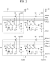
- FIG. 2 is an equivalent circuit diagram of pixels of the solid-state imaging device according to the present embodiment.
- FIG. 3 , FIG. 5A, and FIG. 5B are plan views of a pixel of the solid-state imaging device according to the present embodiment.
- FIG. 4 is a cross-sectional view of the pixel of the solid-state imaging device according to the present embodiment.
- the imaging device 100 includes a pixel region 10, a vertical scanning circuit 20, a column readout circuit 30, a horizontal scanning circuit 40, a control circuit 50, and an output circuit 60.
- a plurality of pixels 12 are provided arranged in a matrix over a plurality of rows by a plurality of columns.
- a control signal line 14 is arranged extending in the row direction (the horizontal direction in FIG. 1 ).
- the control signal line 14 is connected to respective pixels 12 aligned in the row direction, which is a signal line common to these pixels 12.
- a vertical output line 16 is arranged extending in the column direction (the vertical direction in FIG. 1 ).
- the vertical output line 16 is connected to respective pixels 12 aligned in the column direction, which is a signal line common to these pixels 12.
- the control signal line 14 on each row is connected to the vertical scanning circuit 20.
- the vertical scanning circuit 20 is a circuit unit that supplies, to the pixels 12 via the control signal lines 14, control signals for driving readout circuits in the pixels 12 when reading out pixel signals from the pixels 12.
- One end of the vertical output line 16 on each column is connected to the column readout circuit 30.
- Pixel signals read out from the pixels 12 are input to the column readout circuit 30 via the vertical output lines 16.
- the column readout circuit 30 is a circuit unit that performs predetermined signal processing, for example, signal processing such as an amplification process or an analog-to-digital (AD) conversion process on the pixel signals read out from the pixels 12.
- the column readout circuit 30 may include a differential amplifier circuit, a sample-and-hold circuit, an AD conversion circuit, or the like.
- the horizontal scanning circuit 40 is a circuit unit that supplies, to the column readout circuit 30, control signals for transferring the pixel signals processed in the column readout circuit 30 to the output circuit 60 sequentially on a column basis.
- the control circuit 50 is a circuit unit that supplies control signals for controlling operations and the timings of the operations of the vertical scanning circuit 20, the column readout circuit 30, and the horizontal scanning circuit 40.
- the output circuit 60 is a circuit unit that is formed of a buffer amplifier, a differential amplifier, or the like and outputs the pixel signals read out from the column readout circuit 30 to a signal processing unit outside the solid-state imaging device 100.
- FIG. 2 is a circuit diagram illustrating an example of pixel circuits forming the pixel region 10. While FIG. 2 illustrates four pixels 12 arranged in two rows by two columns out of the pixels 12 forming the pixel region 10, the number of pixels 12 forming the pixel region 10 is not limited in particular.
- Each of the plurality of pixels 12 includes a photoelectric conversion unit D, transfer transistors M1 and M2, a reset transistor M3, an amplifier transistor M4, a select transistor M5, and an overflow transistor M6.
- the photoelectric conversion unit D is a photodiode, for example.
- the anode of the photodiode of the photoelectric conversion unit D is connected to the ground voltage line, and the cathode thereof is connected to the source of the transfer transistor M1 and the source of the overflow transistor M6.
- the drain of the transfer transistor M1 is connected to the source of the transfer transistor M2.
- a capacitance component parasitically coupled to the connection node of the drain of the transfer transistor M1 and the source of the transfer transistor M2 has a function as a charge holding portion.
- FIG. 2 depicts such a capacitance component as a capacitor (C1). This capacitor may be denoted as a holding portion C1 in the following description.
- the drain of the transfer transistor M2 is connected to the source of the reset transistor M3 and the gate of the amplifier transistor M4.
- the connection node of the drain of the transfer transistor M2, the source of the reset transistor M3, and the gate of the amplifier transistor M4 is a so-called floating diffusion (FD) region.
- a capacitance component parasitically coupled to the FD region (floating diffusion capacitor) has a function as a charge holding portion.
- FIG. 2 depicts this capacitance component as a capacitor (C2) connected to the FD region.
- the FD region may be denoted as a holding portion C2 in the following description.
- the drain of the reset transistor M3 and the drain of the amplifier transistor M4 are connected to a power source voltage line (VDD).
- the voltage supplied to the drain of the reset transistor M3 and the voltage supplied to the drain of the amplifier transistor M4 may be the same as each other or may be different from each other.
- the source of the amplifier transistor M4 is connected to the drain of the select transistor M5.
- the source of the select transistor M5 is connected to the vertical output line 16.
- the control signal lines 14 are arranged extending in the row direction (the horizontal direction in FIG. 2 ) for each row of the pixel array of the pixel region 10.
- the control signal lines 14 on each row include a control line GS, a control line TX, a control line RES, a control line SEL, and a control line OFG.
- the control line GS is connected to the gates of the transfer transistors M1 of the pixels 12 aligned in the row direction, respectively, which is a signal line common to these pixels 12.
- the control line TX is connected to the gates of the transfer transistors M2 of the pixels 12 aligned in the row direction, respectively, which is a signal line common to these pixels 12.
- the control line RES is connected to the gates of the reset transistors M3 of the pixels 12 aligned in the row direction, respectively, which is a signal line common to these pixels 12.
- the control line SEL is connected to the gates of the select transistors M5 of the pixels 12 aligned in the row direction, respectively, which is a signal line common to these pixels 12.
- the control line OFG is connected to the gates of the overflow transistors M6 of the pixels 12 aligned in the row direction, respectively, which is a signal line common to these pixels 12. Note that, in FIG. 2 , the name of each control line is appended with a corresponding row number (for example, GS(n), GS(n+1)).
- the control lines GS, the control lines TX, the control lines RES, the control lines SEL, and the control lines OFG are connected to the vertical scanning circuit 20.
- a drive pulse for controlling the transfer transistor M1 is output to the control line GS from the vertical scanning circuit 20.
- a drive pulse for controlling the transfer transistor M2 is output to the control line TX from the vertical scanning circuit 20.
- a drive pulse for controlling the reset transistor M3 is output to the control line RES from the vertical scanning circuit 20.
- a drive pulse for controlling the select transistor M5 is output to the control line SEL from the vertical scanning circuit 20.
- a drive pulse for controlling the overflow transistor M6 is output to the control line OFG from the vertical scanning circuit 20.
- These control signals are supplied from the vertical scanning circuit 20 in accordance with predetermined timing signals from the control circuit 50.
- a logic circuit such as a shift resistor, an address decoder, or the like is used for the vertical scanning circuit 20.
- the vertical output lines 16 are arranged extending in the column direction (the vertical direction in FIG. 2 ) for respective rows of the pixel array of the pixel region 10. Each of the vertical output lines 16 is connected to the sources of the select transistors M5 of the pixels 12 aligned in the column direction, which is a signal line common to these pixels 12. The vertical output line 16 is connected with a current source 18.
- the photoelectric conversion unit D converts (photoelectrically converts) an incident light into charges of an amount in accordance with the light amount and accumulates the generated charges.
- the overflow transistor M6 drains charges accumulated in the photoelectric conversion unit D to the drain thereof.
- the drain OFD of the overflow transistor M6 may be connected to the power source voltage line (VDD).
- the transfer transistor M1 transfers charges held in the photoelectric conversion unit D to the holding portion C1.
- the transfer transistor M1 operates as the global electronic shutter.
- the holding portion C1 holds charges generated by the photoelectric conversion unit D in a position different from the photoelectric conversion unit D.
- the transfer transistor M2 transfers charges held in the holding portion C1 to the holding portion C2.
- the holding portion C2 holds charges transferred from the holding portion C1 and sets the voltage of the input node of an amplifier portion (the gate of the amplifier transistor M4) to a voltage in accordance with the capacitance thereof and the amount of the transferred charges.
- the reset transistor M3 resets the holding portion C2 to a predetermined voltage in accordance with the voltage VDD. In this case, it is also possible to reset the holding portion C1 by turning on the transfer transistor M2. Furthermore, it is also possible to reset the photoelectric conversion unit D by further turning on the transfer transistor M1.
- the select transistor M5 selects the pixel 12 from which a signal is output to the output line 16.
- the amplifier transistor M4 is configured such that the voltage VDD is supplied to the drain and a bias current is supplied to the source from the current source 18 via the select transistor M5, which forms an amplifier portion (a source follower circuit) in which the gate is the input node. Thereby, the amplifier transistor M4 outputs a signal Vout based on charges generated by an incident light to the vertical output line 16. Note that, in FIG. 2 , the signal Vout is appended with the corresponding column number (Vout(m), Vout(m+1)).
- Such a configuration allows charges generated by the photoelectric conversion unit D to be accumulated in the photoelectric conversion unit D while the holding portion C1 is holding charges. This enables an image capturing operation in which exposure periods are matched among the plurality of pixels 12, namely, a so-called global electronic shutter operation.
- electronic shutter means electrical control of accumulation of charges generated by an incident light.
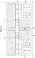
- FIG. 3 illustrates an example of a planar layout of the pixel 12 in the solid-state imaging device according to the present embodiment. While each region where each element of the pixel 12 is provided is depicted with a rectangular block in FIG. 3 for simplified illustration, each block is not intended to illustrate the shape of each element but is intended to illustrate that at least a part of the element is arranged inside each area. For example, regions corresponding to the transfer transistors M1 and M2 and the overflow transistor M6 approximately correspond to regions where the gates of respective transistors are arranged. Further, the region where the reset transistor M3, the amplifier transistor M4, and the select transistor M5 are provided is represented as one region.
- the photoelectric conversion unit D, the transfer transistor M1, the holding portion C1, the transfer transistor M2, and the holding portion C2 are arranged so as to be adjacent to each other in this order within a unit region of the pixel 12.
- the overflow transistor M6 is arranged adjacent to the photoelectric conversion unit D. Arrows depicted in FIG. 3 illustrate a transfer direction of charges when the transfer transistors M1 and M2 and the overflow transistor M6 are driven. That is, when the transfer transistor M1 is driven, charges of the photoelectric conversion unit D are transferred to the holding portion C1. When the transfer transistor M2 is driven, charges of the holding portion C1 are transferred to the holding portion C2. When the overflow transistor M6 is driven, charges of the photoelectric conversion unit D are transferred (drained) to the drain OFD of the overflow transistor M6.
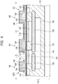
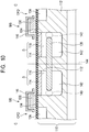
- FIG. 4 is a schematic cross-sectional view taken along the line A-A' of FIG. 3 .
- a p-type semiconductor region 112 (seventh semiconductor region) forming a well is provided on the surface of an n-type semiconductor substrate 110.
- the p-type is a first conductivity type and the n-type is a second conductivity type.
- the photoelectric conversion unit D, the holding portion C1, an n-type semiconductor region 122, and an n-type semiconductor region 124 are arranged spaced apart from each other on the surface of the p-type semiconductor region 112. Note that the description of the reset transistor M3, the amplifier transistor M4, and the select transistor M5 that do not appear in the cross-section of FIG. 4 are omitted here.
- the photoelectric conversion unit D is a buried photodiode including a p-type semiconductor region 114 (first semiconductor region) in contact with the surface of the semiconductor substrate 110 and an n-type semiconductor region 116 (second semiconductor region) provided under the p-type semiconductor region 114.
- the n-type semiconductor region 116 is a charge accumulation layer for accumulating signal charges (electrons) generated by the photoelectric conversion unit D.
- the holding portion C1 has the buried photodiode structure including a p-type semiconductor region 118 (eighth semiconductor region) in contact with the surface of the semiconductor substrate 110 and an n-type semiconductor region 120 (fifth semiconductor region) provided under the p-type semiconductor region 118.
- the n-type semiconductor region 122 forms the holding portion C2.
- the n-type semiconductor region 124 forms the drain OFD of the overflow transistor M6.
- a gate electrode 128 is provided with a gate insulating film 126 interposed therebetween.
- the transfer transistor M1 is formed in which the n-type semiconductor region 116 is the source, the n-type semiconductor region 120 is the drain, and the gate electrode 128 is the gate.
- a gate electrode 132 is provided with a gate insulating film 130 interposed therebetween.
- the transfer transistor M2 is formed in which the n-type semiconductor region 120 is the source, the n-type semiconductor region 122 is the drain, and the gate electrode 132 is the gate.
- a gate electrode 136 is provided with a gate insulating film 134 interposed therebetween.
- the overflow transistor M6 is formed in which the n-type semiconductor region 116 is the source, the n-type semiconductor region 124 is the drain, and the gate electrode 136 is the gate.
- the photoelectric conversion unit D further includes a p-type semiconductor region 138 (third semiconductor region) provided under the n-type semiconductor region 116. Further, the holding portion C1 further includes a p-type semiconductor region 138 (sixth semiconductor region) provided under the n-type semiconductor region 120.
- the p-type semiconductor region 138 has a function as a depletion suppression layer for suppressing the depletion layer from expanding downward from the n-type semiconductor regions 116 and 120 and has a higher impurity concentration than the p-type semiconductor region 112.
- an opening 140 is provided in a part of a region overlapping with the n-type semiconductor region 116 in a plan view.
- plan view refers to a two-dimensional plan view obtained by projecting each component portion of the solid-state imaging device on a plane parallel to the surface of the semiconductor substrate 110, which corresponds to a planar layout of FIG. 3 , for example.
- the p-type semiconductor region 138 is configured to be able to fix the potential thereof. From such a point of view, the p-type semiconductor region 138 is extended in the direction parallel to the surface of the semiconductor substrate 110 and connected to the p-type semiconductor region 112 in the present embodiment. Such a configuration allows the potential of the p-type semiconductor region 138 to be fixed to the potential of the p-type semiconductor region 112 as a well, for example, to the ground potential. Note that a form of connecting the p-type semiconductor region 138 to the p-type semiconductor region 112 is not limited to the example of the present embodiment. For example, a part of the bottom of the p-type semiconductor region 138 may be extended in the depth direction so as to penetrate the n-type semiconductor region 142 and connected to the p-type semiconductor region 112.
- FIG. 5A illustrates the plan view of FIG. 3 overlapped with the p-type semiconductor region 138.
- the p-type semiconductor region 138 is approximately arranged under the photoelectric conversion unit D, the holding portion C1, and the gates of the transfer transistors M1 and M2 and the overflow transistor M6. It is desirable for the opening 140 to be arranged on the holding portion C1 side of a center part 144 of the photoelectric conversion unit D.
- the center part 144 of the photoelectric conversion unit D in this case may be the centroid of the n-type semiconductor region 116 in the plan view, may be the center of the opening region not covered with interconnections or the like, or may be the center of an optical waveguide when the optical waveguide is arranged over the photoelectric conversion unit D.
- the center part 144 is located in substantially the same position of the photoelectric conversion unit D when any of the above definitions is applied.
- a light entering the pixel 12 is converged to the center part 144 of the photoelectric conversion unit D by a microlens (not illustrated) provided above the photoelectric conversion unit D.
- the photoelectric conversion unit D further includes an n-type semiconductor region 142 (fourth semiconductor region) provided under the p-type semiconductor region 138.
- the n-type semiconductor region 142 is provided in at least a region overlapping with the n-type semiconductor region 116 in the plan view.
- the n-type semiconductor region 142 is provided so as to extend from a region overlapping with the n-type semiconductor region 116 in the plan view to a region overlapping with the n-type semiconductor region 120 of the holding portion C1 in the plan view.
- the n-type semiconductor region 116 and the n-type semiconductor region 142 are connected to each other via the opening 140 to form a continuous n-type semiconductor region.
- the n-type semiconductor region 120 and the n-type semiconductor region 142 are separated from each other by the p-type semiconductor region 138.
- the n-type semiconductor regions 142 of the adjacent pixels 12 are separated from each other by the p-type semiconductor region 112.
- the p-type semiconductor region 138 provided under the n-type semiconductor region 116 and the p-type semiconductor region 138 provided under the n-type semiconductor region 120 are provided at the same depth. Further, it can be said that, between the p-type semiconductor region 138 provided under the n-type semiconductor region 116 and the p-type semiconductor region 138 provided under the n-type semiconductor region 120, a region having a lower potential than each of these two p-type semiconductor regions 138 is present.
- FIG. 4 illustrates the light-shielding film 146 provided above the semiconductor substrate 110.
- the light-shielding film 146 is arranged to cover at least the entire holding portion C1 with a metal film having an opening 148 in the center region including at least the center part 144 of the photoelectric conversion unit D.
- FIG. 5B illustrates the plan view of FIG. 3 overlapped with a region where the light-shielding film 146 is provided. Note that, in FIG. 5B , depiction of the gate electrodes 128, 132, and 136 or the contact portions connected to the n-type semiconductor regions 122 and 124 is omitted. In the solid-state imaging device according to the present embodiment, it is preferable for the opening 140 provided in the p-type semiconductor region 138 to be covered with the light-shielding film 146 as illustrated in FIG. 5B , for example.
- the concentration is designed such that, even when electrons are accumulated in the n-type semiconductor region 116, the most part of the n-type semiconductor region 142 is depleted.
- the concentration is designed such that the entire p-type semiconductor region 138 is not depleted.
- the impurity concentration of each portion can be set.
- the impurity concentration boron concentration
- the impurity concentration (arsenic concentration) is 2.5 ⁇ 10 17 cm -3 , and the peak position of the impurity concentration is at a depth of 0.2 ⁇ m.
- the impurity concentration (arsenic concentration) is 2.5 ⁇ 10 17 cm -3 , and the peak position of the impurity concentration is at a depth of 0.2 ⁇ m.
- the impurity concentration (boron concentration) is 1.0 ⁇ 10 16 cm -3 , the peak position of the impurity concentration is at a depth of 0.7 ⁇ m, and the thickness is 0.8 ⁇ m.
- the impurity concentration (phosphorous concentration) is 4.0 ⁇ 10 14 cm -3 , and the depth of the bottom (interface with the p-type semiconductor region 112) is at 3.0 ⁇ m.
- the p-type semiconductor region 138 is provided under the n-type semiconductor region 116 forming a charge accumulation layer of the photoelectric conversion unit D.
- One of the purposes of providing the p-type semiconductor region 138 is to increase the saturation charge amount of the n-type semiconductor region 116 as a charge accumulation layer.
- a p-n junction capacitor is formed between the n-type semiconductor region 116 and the p-type semiconductor region 138.
- Signal charges accumulated in the n-type semiconductor region 116 are transferred to a signal output portion.
- the potential of the n-type semiconductor region 116 reaches a predetermined potential determined by the power source voltage or the like, the signal charges of the n-type semiconductor region 116 are no longer transferred.
- the saturation charge amount increases in proportion to the p-n junction capacitance of the photoelectric conversion unit D. Therefore, by providing the p-type semiconductor region 138, it is possible to increase the saturation charge amount of the n-type semiconductor region 116 as a charge accumulation layer.
- the holding portion C1 may be accumulating signal charges of the previous frame during an exposure period of the photoelectric conversion unit D.
- signal charges based on a light entering the photoelectric conversion unit D leaks into the n-type semiconductor region 120, which may be superimposed on the signal of the previous frame as a noise.
- a light converged into the center part 144 of the photoelectric conversion unit D has expansion of the same degree as the wavelength. While the most part of the light transmitted inside the device is absorbed in the n-type semiconductor region 116 and the p-type semiconductor region 114 of the photoelectric conversion unit D, a non-negligible amount of light enters the p-type semiconductor region 138. As a result, pairs of electrons and holes occur also in the p-type semiconductor region 138 by photoelectric conversion. Although the inside of the p-type semiconductor region 138 is a neutral region and there is no electric field, a small portion of electrons generated in the p-type semiconductor region 138 is diffused and leaks into the holding portion C1.
- the n-type semiconductor region 142 is provided under the p-type semiconductor region 138.
- the concentration is designed so that the most part of the n-type semiconductor region 142 is depleted. Further, the concentration is designed so that the entire p-type semiconductor region 138 is not depleted.
- Japanese Patent Application Laid-Open No. 2014-165286 discloses that a p-type semiconductor region is arranged under an n-type semiconductor region forming a charge accumulation layer of a photoelectric conversion unit.
- a p-type semiconductor region p-type well
- these p-type semiconductor regions are not depleted. Therefore, if the structure disclosed in Japanese Patent Application Laid-Open No. 2014-165286 were simply applied to a solid-state imaging device having the holding portion C1, such configuration could not prevent electrons generated in the p-type semiconductor region under the charge accumulation layer from being scattered and leaking into the holding portion C1.
- the opening 140 serves as a moving path of signal charges when the signal charges generated inside a region deeper than the n-type semiconductor region 116, for example, the n-type semiconductor region 142 are collected to the n-type semiconductor region 116. Therefore, with the opening 140 being provided in the p-type semiconductor region 138, the light-receiving sensitivity can be improved compared to a case where the opening 140 is not provided.
- the opening 140 not to include the center portion 144 of the photoelectric conversion D and to be arranged in a position near the holding portion C1. Since the strongest light enters the center part 144 of the photoelectric conversion unit D, the number of charges generated in the p-type semiconductor region 138 is larger. With the opening 140 being provided in a position closer to the holding portion C1 than to the center part 144 of the photoelectric conversion unit D, electrons generated in the p-type semiconductor region 138 near the center part 144 of the photoelectric conversion unit D are pulled into the potential of the opening 140 before reaching the holding portion C1. The electrons pulled into the potential of the opening 140 are captured by the n-type semiconductor region 116 or the n-type semiconductor region 142. Therefore, such an arrangement can further reduce a noise component leaking into the holding portion C1.
- the opening 140 in a position that does not overlap with a light incident region.
- the n-type semiconductor region 142 may be arranged to extend up to under the holding portion C1 as previously described. A small part of a light entering the pixel 12 further enters the under part of the holding portion C1 due to scattering or the like. The n-type semiconductor region 142 extends up to under holding portion C1 and thereby the photoelectric conversion region of a deeper part expands, which allows electrons generated under the holding portion C1 to be also collected in the n-type semiconductor region 116. Thereby, the light-receiving sensitivity can be further improved.
- the p-type semiconductor region 138 extending under the n-type semiconductor region 120 provides an advantage of increasing the saturation charge amount of the n-type semiconductor region 120 as a charge accumulation layer in the holding portion C1 similarly to the case of the n-type semiconductor region 116.
- no opening is provided in the p-type semiconductor region 138 between the n-type semiconductor region 120 and the n-type semiconductor region 142, and the n-type semiconductor region 120 is separated from the n-type semiconductor region 142.
- Such a configuration can prevent charges generated in the n-type semiconductor region 142 and a deeper region thereof from flowing into the n-type semiconductor region 120.
- the p-type semiconductor region 138 can be formed by implanting impurity ions with a photoresist opened in a predetermined region as a mask.
- the opening 140 can be formed by covering in advance a part of a region overlapping with the n-type semiconductor region 116 by the photoresist in the plan view.
- the impurity concentration of the p-type semiconductor region 138 may be different between a region under the n-type semiconductor region 116 and a region under the n-type semiconductor region 120. By doing so, it is possible to design the p-type semiconductor region 138 in accordance with characteristics required for the photoelectric conversion unit D and the holding portion C1 to improve the flexibility of design.
- the p-type semiconductor region 138 at the same time as the formation of the region under the n-type semiconductor region 116 and the region under the n-type semiconductor region 120 in view of reduction in manufacturing cost.
- the p-type semiconductor region 138 under the n-type semiconductor region 116 and the p-type semiconductor region 138 under the n-type semiconductor region 120 will be formed at the same depth of the semiconductor substrate and at the same impurity concentration.
- charges generated in the p-type semiconductor region 138 can be collected in the n-type semiconductor region 116 of the photoelectric conversion unit D. This can improve the sensitivity of the photoelectric conversion unit D and prevent unintended charges from leaking into the holding portion C1.
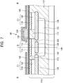
- FIG. 6 is a plan view of a pixel of the solid-state imaging device according to the present embodiment.
- FIG. 7 is a cross-sectional view of the pixel of the solid-state imaging device according to the present embodiment.
- FIG. 8 is a plan view of a pixel of a solid-state imaging device according to a modified example of the present embodiment. Similar component as that of the solid-state imaging device according to the first embodiment is labeled with the same reference symbol, and the description thereof will be omitted or simplified.
- the pixels 12 having the planar layout illustrated in FIG. 3 are arranged adjacent to each other in the vertical direction in the drawing.
- the photoelectric conversion unit D of the pixel 12A is arranged adjacent to the holding portion C1 of the pixel 12B.
- leakage of signal charges from the p-type semiconductor region 138 of the photoelectric conversion unit D of the pixel A into the holding portion C1 of the pixel 12B may occur.
- FIG. 7 is a schematic cross-sectional view taken along the line B-B' of FIG. 6 .
- the n-type semiconductor region 116 is connected to the n-type semiconductor region 142 via the two openings 140 in the outside of the center part 144 of the photoelectric conversion unit D.
- an opening 140 may be arranged to surround a region including the center part 144 of the photoelectric conversion unit D in the plan view as illustrated in FIG. 8 , for example.
- a fixed voltage supply to the p-type semiconductor region 138 can be realized by forming a part of the bottom of the p-type semiconductor region 138 to extend in the depth direction and connect to the p-type semiconductor region 112.
- charges generated in the p-type semiconductor region 138 can be collected in the n-type semiconductor region 116 of the photoelectric conversion unit D. This can improve the sensitivity of the photoelectric conversion unit D and prevent unintended charges from leaking into the holding portion C1.
- FIG. 9 is a plan view of a pixel of a solid-state imaging device according to the present embodiment.
- FIG. 10 is a cross-sectional view of the pixel of the solid-state imaging device according to the present embodiment. Similar component as that of the solid-state imaging device according to the first and second embodiments is labeled with the same reference symbol, and the description thereof will be omitted or simplified.
- the pixels 12 having the planar layout illustrated in FIG. 3 are arranged mirror-symmetrically and adjacent to each other in the horizontal direction in the drawing.
- the photoelectric conversion unit D of the pixel 12A is arranged adjacent to the photoelectric conversion unit D of the pixel 12B.
- the openings 140 are arranged to surround a region including the center part 144 of the photoelectric conversion unit D in the plan view, some improvement is required, such as forming the bottom of the p-type semiconductor region 138 to extend in the depth direction and connect to the p-type semiconductor region 112 as described in the modified example of the second embodiment.
- FIG. 10 is a schematic cross-sectional view taken along the line C-C' of FIG. 9 .
- FIG. 10 illustrates a state where the p-type semiconductor region 138 and the p-type semiconductor region 112 are connected at the boundary between the pixel 12A and the pixel 12B.
- the layout of the present embodiment can be applied to a pixel used for focus detection.
- a single microlens (not illustrated) that converges a light into the pixel 12 is arranged to the photoelectric conversion unit D of the pixel 12A and the photoelectric conversion unit D of the pixel 12B.
- the center 150 of a light converged by the microlens is arranged between the photoelectric conversion unit D of the pixel 12A and the photoelectric conversion unit D of the pixel 12B.
- charges generated in the p-type semiconductor region 138 can be collected into the n-type semiconductor region 116 of the photoelectric conversion unit D. This can improve the sensitivity of the photoelectric conversion unit D and prevent unintended charges from leaking into the holding portion C1.
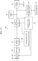
- FIG. 11 is a block diagram illustrating a configuration of the imaging system according to the present embodiment.
- the imaging devices 100 described in the above first to the third embodiments can be applied to various imaging systems.
- the applicable imaging systems may include a digital still camera, a digital camcorder, a surveillance camera, a copier machine, a fax machine, a mobile phone, an on-vehicle camera, an observation satellite, and the like.
- a camera module having an optical system, such as a lens, and an imaging device may be included in the imaging system.
- FIG. 11 illustrates a block diagram of a digital still camera as an example of the above.
- the imaging system 200 illustrated as an example in FIG. 11 has the imaging device 201, a lens 202 that captures an optical image of a subject onto the imaging device 201, an aperture 204 for changing a light amount passing through the lens 202, and a barrier 206 for protecting the lens 202.
- the lens 202 and the aperture 204 form an optical system that converges a light onto the imaging device 201.
- the imaging device 201 is any of the solid-state imaging devices 100 described in the first to third embodiments and converts an optical image captured by the lens 202 into image data.
- the imaging system 200 further has a signal processing unit 208 that processes an output signal output from the imaging device 201.
- the signal processing unit 208 performs AD conversion that converts an analog signal output from the imaging device 201 into a digital signal. Further, the signal processing unit 208 performs other operations of performing various correction or compression if necessary and outputting image data.
- An AD conversion unit that is a part of the signal processing unit 208 may be formed on the semiconductor substrate in which the imaging device 201 is provided, or may be formed on a different semiconductor substrate from the imaging device 201. Further, the imaging device 201 and the signal processing unit 208 may be formed on the same semiconductor substrate.
- the imaging system 200 further has a memory unit 210 for temporarily storing image data therein and an external interface unit (external I/F unit) 212 for communicating with an external computer or the like.
- the imaging system 200 further has a storage medium 214 such as a semiconductor memory for performing storage or readout of image pickup data and a storage medium control interface unit (storage medium control I/F unit) 216 for performing storage or readout on the storage medium 214.
- the storage medium 214 may be embedded in the imaging system 200 or may be removable.
- the imaging system 200 further has a general control/operation unit 218 that controls various computation and controls the entire digital still camera and a timing generation unit 220 that outputs various timing signals to the imaging device 201 and the signal processing unit 208.
- the timing signal or the like may be input from the outside, and the imaging system 200 may have at least the imaging device 201 and the signal processing unit 208 that processes an output signal output from the imaging device 201.
- the imaging device 201 outputs an imaging signal to the signal processing unit 208.
- the signal processing unit 208 performs predetermined signal processing on the imaging signal output from the imaging device 201 and outputs image data.
- the signal processing unit 208 uses the imaging signal to generate an image.
- Solid-state imaging device 100 can realize an imaging system that can acquire a good quality image with a high sensitivity and a large saturation charge amount.
- FIG. 12A is a diagram illustrating a configuration of the imaging system according to the present embodiment.
- FIG. 12B is a diagram illustrating a configuration of the movable object according to the present embodiment.
- FIG. 12A illustrates an example of an imaging system related to an on-vehicle camera.
- the imaging system 300 has an imaging device 310.
- the imaging device 310 is any of the solid-state imaging devices 100 described in the above first to third embodiments.
- the imaging system 300 has an image processing unit 312 that performs image processing on a plurality of image data acquired by the imaging device 310 and a parallax calculation unit 314 that calculates a parallax (a phase difference of parallax images) from the plurality of image data acquired by the imaging system 300.
- the imaging system 300 has a distance measurement unit 316 that calculates a distance to the object based on the calculated parallax and a collision determination unit 318 that determines whether or not there is a collision possibility based on the calculated distance.
- the parallax calculation unit 314 and the distance measurement unit 316 are an example of a distance information acquisition unit that acquires distance information on the distance to the object. That is, the distance information is information on a parallax, a defocus amount, a distance to an object, or the like.
- the collision determination unit 318 may use any of the distance information to determine the collision possibility.
- the distance information acquisition unit may be implemented by dedicatedly designed hardware or may be implemented by a software module. Further, the distance information acquisition unit may be implemented by a Field Programmable Gate Array (FPGA), an Application Specific Integrated Circuit (ASIC), or the like, or may be implemented by combination thereof.
- FPGA Field Programmable Gate Array
- ASIC Application Specific Integrated Circuit
- the imaging system 300 is connected to the vehicle information acquisition device 320 and can acquire vehicle information such as a vehicle speed, a yaw rate, a steering angle, or the like. Further, the imaging system 300 is connected with a control ECU 330, which is a control device that outputs a control signal for causing a vehicle to generate braking force based on a determination result by the collision determination unit 318. Further, the imaging system 300 is connected with an alert device 340 that issues an alert to the driver based on a determination result by the collision determination unit 318.
- the control ECU 330 performs vehicle control to avoid a collision or reduce damage by applying a brake, pushing back an accelerator, suppressing engine power, or the like.
- the alert device 340 alerts a user by sounding an alert such as a sound, displaying alert information on a display of a car navigation system or the like, providing vibration to a seat belt or a steering wheel, or the like.
- an area around a vehicle for example, a front area or a rear area is captured by using the imaging system 300.
- FIG. 12B illustrates the imaging system in a case of capturing a front area of a vehicle (a capturing area 350).
- the vehicle information acquisition device 320 transmits instructions to the imaging system 300 or the imaging device 310. Such a configuration can further improve the ranging accuracy.
- the embodiment is applicable to automatic driving control for following another vehicle, automatic driving control for not going out of a traffic lane, or the like.
- the imaging system is not limited to a vehicle such as the subject vehicle, and can be applied to a movable object (moving apparatus) such as a ship, an airplane, or an industrial robot, for example.
- the imaging system can be widely applied to a device which utilizes object recognition, such as an intelligent transportation system (ITS), without being limited to movable objects.
- ITS intelligent transportation system
- an example in which a part of the configuration of any of the embodiments is added to another embodiment or an example in which a part of the configuration of any of the embodiments is replaced with a part of the configuration of another embodiment is one of the embodiments of the present invention.
- the conductivity type of the semiconductor region forming each portion of the pixel 12 is the opposite conductivity type.
- the names of source and drain of each transistor described in the above embodiments may be different in accordance with the conductivity of the transistor, the function in interest, or the like, and all or a part of the sources and drains described above may be referenced by the opposite names.
- the holding portion C1 has the buried diode structure including the p-type semiconductor region 118 and the n-type semiconductor region 120 in the above embodiments, the configuration of the holding portion C1 is not limited thereto.
- an electrode may be arranged over the semiconductor substrate 110 via an insulating film without the p-type semiconductor region 118 being arranged on the surface of the semiconductor substrate 110, and a MOS capacitor may be formed between the electrode and the n-type semiconductor region 120. This electrode may be connected to the gate electrode 128 of the transfer transistor M1.
- the present invention can be widely applied to solid-state imaging devices having a holding portion used for temporarily holding signal carriers separately from a photoelectric conversion unit.
- the imaging system illustrated in the above embodiments are an example of imaging systems to which the solid-state imaging device of the present invention may be applied, the imaging system to which the solid-state imaging device of the present invention can be applied is not limited to the configuration illustrated in FIG. 11 to FIG. 12B .
Landscapes
- Engineering & Computer Science (AREA)
- Multimedia (AREA)
- Signal Processing (AREA)
- Automation & Control Theory (AREA)
- Transportation (AREA)
- Mechanical Engineering (AREA)
- Solid State Image Pick-Up Elements (AREA)
- Transforming Light Signals Into Electric Signals (AREA)
Claims (10)
- Festkörperabbildungsvorrichtung (100), mit:einer Vielzahl von Pixeln (12), wovon jedes eine fotoelektrische Umwandlungseinheit (D) umfasst, die Ladungen durch fotoelektrische Umwandlung erzeugt;einem ersten Halteabschnitt (C1), der Ladungen hält, die von der fotoelektrischen Umwandlungseinheit (D) übertragen werden;einem zweiten Halteabschnitt (C2), der Ladungen hält, die von dem ersten Halteabschnitt (C1) übertragen werden; undeiner Verstärkungseinheit, die ein Signal auf Grundlage einer Menge von durch den zweiten Halteabschnitt (C2) gehaltenen Ladungen ausgibt, wobei die fotoelektrische Umwandlungseinheit (D) umfasstein erstes Halbleitergebiet (114) einer ersten Leitfähigkeitsart, das in einem Halbleitersubstrat (110) bereitgestellt ist und in Kontakt mit einer Oberfläche des Halbleitersubstrats (110) ist,ein zweites Halbleitergebiet (116) einer zweiten Leitfähigkeitsart, das unter dem ersten Halbleitergebiet (114) bereitgestellt ist und dazu angepasst ist, um die erzeugten Ladungen zu akkumulieren,ein drittes Halbleitergebiet (138) der ersten Leitfähigkeitsart, das unter dem zweiten Halbleitergebiet (116) bereitgestellt ist, wobei eine Störstellenkonzentration des dritten Halbleitergebiets (138) derart eingestellt ist, dass die Gesamtheit des dritten Halbleitergebiets (138) nicht verarmt ist, undein viertes Halbleitergebiet (142) der zweiten Leitfähigkeitsart, das unter dem dritten Halbleitergebiet (138) bereitgestellt ist, wobei eine Störstellenkonzentration des vierten Halbleitergebiets (142) derart eingestellt ist, dass das vierte Halbleitergebiet (142) verarmt ist, wenn Ladungen in dem zweiten Halbleitergebiet (116) akkumuliert werden,wobei das dritte Halbleitergebiet (138) eine Öffnung (140) in einem Gebiet aufweist, das in einer Draufsicht mit dem zweiten Halbleitergebiet (116) überlappt, und das zweite Halbleitergebiet (116) und das vierte Halbleitergebiet (142) über die Öffnung (140) verbunden sind,wobei das vierte Halbleitergebiet (142) ausbreitend unter einem sechsten Halbleitergebiet (138) bereitgestellt ist,wobei der erste Halteabschnitt (C1) umfasstein fünftes Halbleitergebiet (120) der zweiten Leitfähigkeitsart, das beabstandet von dem zweiten Halbleitergebiet (116) bereitgestellt ist, unddas sechste Halbleitergebiet (138) der ersten Leitfähigkeitsart, das unter dem fünften Halbleitergebiet (120) bei einer Tiefe bereitgestellt ist, bei der das dritte Halbleitergebiet (138) bereitgestellt ist, undwobei das zweite Halbleitergebiet (116) und das vierte Halbleitergebiet (142) über die Öffnung (140) miteinander verbunden sind, um ein durchgehendes Halbleitergebiet auszubilden, sodass das durchgängige Halbleitergebiet, das ein geringeres Potenzial als sowohl das dritte Halbleitergebiet (138) als auch das sechste Halbleitergebiet (138) aufweist, zwischen dem dritten Halbleitergebiet (138) und dem sechsten Halbleitergebiet (138) bereitgestellt ist,dadurch gekennzeichnet, dassin einer Draufsicht, die Öffnung (140) innerhalb eines Bereichs zwischen einem Mittelabschnitt der fotoelektrischen Umwandlungseinheit (D) und dem ersten Halteabschnitt (C1) angeordnet ist.
- Festkörperabbildungsvorrichtung (100) nach Anspruch 1, wobei die Öffnung (140) zwischen dem Mittelabschnitt der fotoelektrischen Umwandlungseinheit (D) und dem ersten Halteabschnitt (C1) von einem anderen benachbarten Pixel in einer Draufsicht angeordnet ist.
- Festkörperabbildungsvorrichtung (100) nach einem der Ansprüche 1 oder 2, ferner mit einer Lichtabschirmungsschicht (146), die den ersten Halteabschnitt (C1) bedeckt,
wobei sich die Lichtabschirmungsschicht (146) über der Öffnung (140) erstreckt. - Festkörperabbildungsvorrichtung (100) nach einem der Ansprüche 1 bis 3, wobei das dritte Halbleitergebiet (138) und das sechste Halbleitergebiet (138) die gleiche Störstellenkonzentration aufweisen.
- Festkörperabbildungsvorrichtung (100) nach einem der Ansprüche 1 bis 4, wobei die fotoelektrische Umwandlungseinheit (D) von einem Pixel und die fotoelektrische Umwandlungseinheit (D) eines anderen Pixels nebeneinander angeordnet sind, und das dritte Halbleitergebiet (138) des ersten Pixels und das dritte Halbleitergebiet (138) des anderen Pixels miteinander verbunden sind.
- Festkörperabbildungsvorrichtung (100) nach einem der Ansprüche 1 bis 5,
wobei die fotoelektrische Umwandlungseinheit (D) und der erste Halteabschnitt (C1) in einem siebten Halbleitergebiet (112) der ersten Leitfähigkeitsart bereitgestellt sind, und
wobei das dritte Halbleitergebiet (138) und das sechste Halbleitergebiet (138) mit dem siebten Halbleitergebiet verbunden sind. - Festkörperabbildungsvorrichtung (100) nach Anspruch 6, wobei das dritte Halbleitergebiet (138) und das sechste Halbleitergebiet (138) jeweils eine höhere Störstellenkonzentration als das siebte Halbleitergebiet (112) aufweisen.
- Festkörperabbildungsvorrichtung (100) nach einem der Ansprüche 1 bis 7,
wobei der erste Halteabschnitt (C1) ferner ein achtes Halbleitergebiet (118) der ersten Leitfähigkeitsart umfasst, das in dem Halbleitersubstrat (110) und in Kontakt mit einer Oberfläche des Halbleitersubstrats (110) bereitgestellt ist, und
wobei das fünfte Halbleitergebiet (120) unter dem achten Halbleitergebiet (118) bereitgestellt ist. - Abbildungssystem, mit:der Festkörperabbildungsvorrichtung (100) nach einem der Ansprüche 1 bis 8; undeiner Signalverarbeitungseinheit (208), die die Signale verarbeitet, die von den Pixeln der Festkörperabbildungsvorrichtung (100) ausgegeben werden.
- Bewegliches Objekt, mit:der Festkörperabbildungsvorrichtung (100, 310) nach einem der Ansprüche 1 bis 8;einer Abstandsinformationserfassungseinheit (314, 316), die dazu angepasst ist, um eine Abstandsinformation über einen Abstand zu einem Objekt auf Grundlage von Signalen von der Festkörperabbildungsvorrichtung (100, 310) aus Paralaxenbildern zu erfassen; undeiner Steuerungseinheit (330), die dazu angepasst ist, um das bewegliche Objekt auf Grundlage der Abstandsinformation zu steuern.
Applications Claiming Priority (1)
| Application Number | Priority Date | Filing Date | Title |
|---|---|---|---|
| JP2017054074A JP6701108B2 (ja) | 2017-03-21 | 2017-03-21 | 固体撮像装置及び撮像システム |
Publications (3)
| Publication Number | Publication Date |
|---|---|
| EP3379575A2 EP3379575A2 (de) | 2018-09-26 |
| EP3379575A3 EP3379575A3 (de) | 2018-10-17 |
| EP3379575B1 true EP3379575B1 (de) | 2021-05-12 |
Family
ID=61655624
Family Applications (1)
| Application Number | Title | Priority Date | Filing Date |
|---|---|---|---|
| EP18161673.1A Active EP3379575B1 (de) | 2017-03-21 | 2018-03-14 | Festkörperbildgebungsvorrichtung, bildgebungssystem und bewegliches objekt |
Country Status (7)
| Country | Link |
|---|---|
| US (1) | US10453879B2 (de) |
| EP (1) | EP3379575B1 (de) |
| JP (1) | JP6701108B2 (de) |
| KR (1) | KR102262794B1 (de) |
| CN (1) | CN108632544B (de) |
| BR (1) | BR102018005471A2 (de) |
| RU (1) | RU2688958C1 (de) |
Families Citing this family (16)
| Publication number | Priority date | Publication date | Assignee | Title |
|---|---|---|---|---|
| JP7091080B2 (ja) | 2018-02-05 | 2022-06-27 | キヤノン株式会社 | 装置、システム、および移動体 |
| JP7108421B2 (ja) | 2018-02-15 | 2022-07-28 | キヤノン株式会社 | 撮像装置及び撮像システム |
| JP7019471B2 (ja) | 2018-03-19 | 2022-02-15 | キヤノン株式会社 | 固体撮像装置及び撮像システム |
| JP7161317B2 (ja) | 2018-06-14 | 2022-10-26 | キヤノン株式会社 | 撮像装置、撮像システム及び移動体 |
| JP6929266B2 (ja) | 2018-12-17 | 2021-09-01 | キヤノン株式会社 | 光電変換装置、光電変換システム、移動体 |
| JP7292868B2 (ja) | 2018-12-18 | 2023-06-19 | キヤノン株式会社 | 検出器 |
| JP2020107980A (ja) | 2018-12-27 | 2020-07-09 | キヤノン株式会社 | 光検出装置および撮像システム |
| JP7555703B2 (ja) | 2019-02-25 | 2024-09-25 | キヤノン株式会社 | 光電変換装置、撮像システム及び移動体 |
| US11503234B2 (en) * | 2019-02-27 | 2022-11-15 | Canon Kabushiki Kaisha | Photoelectric conversion device, imaging system, radioactive ray imaging system, and movable object |
| US20210305303A1 (en) * | 2020-03-31 | 2021-09-30 | Canon Kabushiki Kaisha | Photoelectric conversion apparatus, photoelectric conversion system, and moving object |
| JP7019743B2 (ja) * | 2020-04-08 | 2022-02-15 | キヤノン株式会社 | 固体撮像装置及び撮像システム |
| JP7170100B2 (ja) * | 2020-08-07 | 2022-11-11 | キヤノン株式会社 | 撮像素子及び撮像装置 |
| JP7534902B2 (ja) | 2020-09-23 | 2024-08-15 | キヤノン株式会社 | 光電変換装置、撮像装置、半導体装置及び光電変換システム |
| JP7753044B2 (ja) | 2021-10-20 | 2025-10-14 | キヤノン株式会社 | 光電変換装置 |
| JP2024009651A (ja) | 2022-07-11 | 2024-01-23 | キヤノン株式会社 | 光電変換装置、撮像システム、および機器 |
| JP2024073685A (ja) | 2022-11-18 | 2024-05-30 | キヤノン株式会社 | 光電変換装置及びその駆動方法 |
Citations (1)
| Publication number | Priority date | Publication date | Assignee | Title |
|---|---|---|---|---|
| US20150054997A1 (en) * | 2013-08-23 | 2015-02-26 | Aptina Imaging Corporation | Image sensors having pixel arrays with non-uniform pixel sizes |
Family Cites Families (44)
| Publication number | Priority date | Publication date | Assignee | Title |
|---|---|---|---|---|
| JP3723124B2 (ja) | 2001-12-14 | 2005-12-07 | 株式会社東芝 | 固体撮像装置 |
| JP2005209673A (ja) | 2004-01-20 | 2005-08-04 | Sony Corp | 光電変換装置および光電変換装置の製造方法および固体撮像装置 |
| JP2008004692A (ja) * | 2006-06-21 | 2008-01-10 | Nikon Corp | 固体撮像装置 |
| JP4818018B2 (ja) | 2006-08-01 | 2011-11-16 | キヤノン株式会社 | 光電変換装置及びそれを用いた撮像システム |
| JP5132102B2 (ja) | 2006-08-01 | 2013-01-30 | キヤノン株式会社 | 光電変換装置および光電変換装置を用いた撮像システム |
| JP4494492B2 (ja) | 2008-04-09 | 2010-06-30 | キヤノン株式会社 | 固体撮像装置及び固体撮像装置の駆動方法 |
| JP5213501B2 (ja) | 2008-04-09 | 2013-06-19 | キヤノン株式会社 | 固体撮像装置 |
| JP4759590B2 (ja) | 2008-05-09 | 2011-08-31 | キヤノン株式会社 | 光電変換装置及びそれを用いた撮像システム |
| JP5279352B2 (ja) | 2008-06-06 | 2013-09-04 | キヤノン株式会社 | 固体撮像装置 |
| JP4752926B2 (ja) * | 2009-02-05 | 2011-08-17 | ソニー株式会社 | 固体撮像装置、固体撮像装置の製造方法、固体撮像装置の駆動方法、電子機器 |
| JP2010268080A (ja) | 2009-05-12 | 2010-11-25 | Canon Inc | 固体撮像装置 |
| JP4785963B2 (ja) * | 2009-10-09 | 2011-10-05 | キヤノン株式会社 | 固体撮像装置 |
| JP2011222708A (ja) * | 2010-04-08 | 2011-11-04 | Sony Corp | 固体撮像装置、固体撮像装置の製造方法、および電子機器 |
| US8618459B2 (en) * | 2011-04-27 | 2013-12-31 | Aptina Imaging Corporation | Image sensor array for the back side illumination with junction gate photodiode pixels |
| JP2013093553A (ja) | 2011-10-04 | 2013-05-16 | Canon Inc | 光電変換装置及びその製造方法、並びに光電変換システム |
| JP5967944B2 (ja) | 2012-01-18 | 2016-08-10 | キヤノン株式会社 | 固体撮像装置およびカメラ |
| JP6053505B2 (ja) | 2012-01-18 | 2016-12-27 | キヤノン株式会社 | 固体撮像装置 |
| US9490373B2 (en) * | 2012-02-02 | 2016-11-08 | Sony Corporation | Solid-state imaging device and electronic apparatus with improved storage portion |
| JP6004665B2 (ja) * | 2012-02-17 | 2016-10-12 | キヤノン株式会社 | 撮像装置、および撮像システム。 |
| JP2014049727A (ja) | 2012-09-04 | 2014-03-17 | Canon Inc | 固体撮像装置 |
| JP2014165286A (ja) * | 2013-02-23 | 2014-09-08 | Nikon Corp | フォトダイオード、固体撮像素子及び撮像装置 |
| JP5925713B2 (ja) | 2013-02-26 | 2016-05-25 | 株式会社東芝 | 固体撮像装置 |
| US9159753B2 (en) * | 2013-03-01 | 2015-10-13 | Semiconductor Components Industries, Llc | Image sensor pixels with self-aligned lateral anti-blooming structures |
| US9231007B2 (en) * | 2013-08-27 | 2016-01-05 | Semiconductor Components Industries, Llc | Image sensors operable in global shutter mode and having small pixels with high well capacity |
| JP6261361B2 (ja) | 2014-02-04 | 2018-01-17 | キヤノン株式会社 | 固体撮像装置およびカメラ |
| US9479717B2 (en) * | 2014-02-18 | 2016-10-25 | Semiconductor Components Industries, Llc | Image sensor array with external charge detection circuitry |
| JP6595750B2 (ja) | 2014-03-14 | 2019-10-23 | キヤノン株式会社 | 固体撮像装置及び撮像システム |
| JP6274567B2 (ja) | 2014-03-14 | 2018-02-07 | キヤノン株式会社 | 固体撮像装置及び撮像システム |
| JP6541347B2 (ja) | 2014-03-27 | 2019-07-10 | キヤノン株式会社 | 固体撮像装置および撮像システム |
| WO2015187884A1 (en) * | 2014-06-06 | 2015-12-10 | Rambus Inc. | Image sensor with depletion-level pixel charge transfer control |
| JP6417197B2 (ja) | 2014-11-27 | 2018-10-31 | キヤノン株式会社 | 固体撮像装置 |
| JP2016207791A (ja) * | 2015-04-20 | 2016-12-08 | キヤノン株式会社 | 撮像装置の製造方法 |
| US9768213B2 (en) | 2015-06-03 | 2017-09-19 | Canon Kabushiki Kaisha | Solid-state image sensor and camera |
| WO2016203974A1 (ja) * | 2015-06-15 | 2016-12-22 | ソニー株式会社 | イメージセンサ、および電子機器 |
| JP6570384B2 (ja) * | 2015-09-11 | 2019-09-04 | キヤノン株式会社 | 撮像装置及び撮像システム |
| US10205894B2 (en) | 2015-09-11 | 2019-02-12 | Canon Kabushiki Kaisha | Imaging device and imaging system |
| JP6664175B2 (ja) * | 2015-09-11 | 2020-03-13 | キヤノン株式会社 | 撮像装置及び撮像装置の製造方法 |
| JP6541523B2 (ja) | 2015-09-11 | 2019-07-10 | キヤノン株式会社 | 撮像装置、撮像システム、および、撮像装置の制御方法 |
| US9706142B2 (en) * | 2015-09-23 | 2017-07-11 | Semiconductor Components Industries, Llc | High dynamic range and global shutter image sensor pixels having charge overflow signal detecting structures |
| JP2017135168A (ja) | 2016-01-25 | 2017-08-03 | キヤノン株式会社 | 光電変換装置及び情報処理装置 |
| JP6776011B2 (ja) | 2016-06-10 | 2020-10-28 | キヤノン株式会社 | 撮像装置及び撮像システム |
| JP6727938B2 (ja) | 2016-06-10 | 2020-07-22 | キヤノン株式会社 | 撮像装置、撮像装置の制御方法、及び撮像システム |
| JP6688165B2 (ja) * | 2016-06-10 | 2020-04-28 | キヤノン株式会社 | 撮像装置及び撮像システム |
| JP7013119B2 (ja) | 2016-07-21 | 2022-01-31 | キヤノン株式会社 | 固体撮像素子、固体撮像素子の製造方法、及び撮像システム |
-
2017
- 2017-03-21 JP JP2017054074A patent/JP6701108B2/ja active Active
-
2018
- 2018-03-07 US US15/914,505 patent/US10453879B2/en active Active
- 2018-03-14 EP EP18161673.1A patent/EP3379575B1/de active Active
- 2018-03-16 CN CN201810216003.7A patent/CN108632544B/zh active Active
- 2018-03-19 RU RU2018109487A patent/RU2688958C1/ru active
- 2018-03-20 BR BR102018005471A patent/BR102018005471A2/pt not_active Application Discontinuation
- 2018-03-20 KR KR1020180031815A patent/KR102262794B1/ko active Active
Patent Citations (1)
| Publication number | Priority date | Publication date | Assignee | Title |
|---|---|---|---|---|
| US20150054997A1 (en) * | 2013-08-23 | 2015-02-26 | Aptina Imaging Corporation | Image sensors having pixel arrays with non-uniform pixel sizes |
Also Published As
| Publication number | Publication date |
|---|---|
| KR20180106989A (ko) | 2018-10-01 |
| EP3379575A3 (de) | 2018-10-17 |
| JP2018157127A (ja) | 2018-10-04 |
| KR102262794B1 (ko) | 2021-06-09 |
| RU2688958C1 (ru) | 2019-05-23 |
| BR102018005471A2 (pt) | 2018-10-30 |
| CN108632544B (zh) | 2021-04-02 |
| US20180277575A1 (en) | 2018-09-27 |
| JP6701108B2 (ja) | 2020-05-27 |
| CN108632544A (zh) | 2018-10-09 |
| EP3379575A2 (de) | 2018-09-26 |
| US10453879B2 (en) | 2019-10-22 |
Similar Documents
| Publication | Publication Date | Title |
|---|---|---|
| EP3379575B1 (de) | Festkörperbildgebungsvorrichtung, bildgebungssystem und bewegliches objekt | |
| US11553149B2 (en) | Solid-state imaging device, imaging system and movable object | |
| JP7108421B2 (ja) | 撮像装置及び撮像システム | |
| US10818708B2 (en) | Solid-state imaging device and imaging system | |
| US10868069B2 (en) | Solid state imaging device, imaging system, and mobile apparatus | |
| US10381388B2 (en) | Solid-state imaging device and imaging system | |
| US20230069364A1 (en) | Photoelectric conversion apparatus having capacitance addition transistor, photoelectric conversion system, and movable body | |
| US12068342B2 (en) | Photoelectric conversion device, imaging system, and movable body | |
| JP7581020B2 (ja) | 光電変換装置、光電変換システム、移動体 | |
| JP7279105B2 (ja) | 光電変換装置 | |
| US11450701B2 (en) | Photoelectric conversion apparatus, photoelectric conversion system, and movable body | |
| JP7019743B2 (ja) | 固体撮像装置及び撮像システム | |
| JP2022158523A (ja) | 光電変換装置、光電変換システム、移動体 | |
| US12176358B2 (en) | Photoelectric conversion apparatus, photoelectric conversion system, and moving body | |
| US11575822B2 (en) | Photoelectric conversion apparatus, photoelectric conversion system, and moving body | |
| JP6946379B2 (ja) | 固体撮像装置及び撮像システム | |
| JP2023174479A (ja) | 光電変換装置 | |
| JP2021190614A (ja) | 光電変換装置及びその製造方法 | |
| JP2020004804A (ja) | 固体撮像装置、撮像システム、移動体、固体撮像装置の製造方法 |
Legal Events
| Date | Code | Title | Description |
|---|---|---|---|
| PUAI | Public reference made under article 153(3) epc to a published international application that has entered the european phase |
Free format text: ORIGINAL CODE: 0009012 |
|
| STAA | Information on the status of an ep patent application or granted ep patent |
Free format text: STATUS: THE APPLICATION HAS BEEN PUBLISHED |
|
| PUAL | Search report despatched |
Free format text: ORIGINAL CODE: 0009013 |
|
| AK | Designated contracting states |
Kind code of ref document: A2 Designated state(s): AL AT BE BG CH CY CZ DE DK EE ES FI FR GB GR HR HU IE IS IT LI LT LU LV MC MK MT NL NO PL PT RO RS SE SI SK SM TR |
|
| AX | Request for extension of the european patent |
Extension state: BA ME |
|
| AK | Designated contracting states |
Kind code of ref document: A3 Designated state(s): AL AT BE BG CH CY CZ DE DK EE ES FI FR GB GR HR HU IE IS IT LI LT LU LV MC MK MT NL NO PL PT RO RS SE SI SK SM TR |
|
| AX | Request for extension of the european patent |
Extension state: BA ME |
|
| RIC1 | Information provided on ipc code assigned before grant |
Ipc: H01L 27/146 20060101AFI20180911BHEP |
|
| STAA | Information on the status of an ep patent application or granted ep patent |
Free format text: STATUS: REQUEST FOR EXAMINATION WAS MADE |
|
| 17P | Request for examination filed |
Effective date: 20190417 |
|
| RBV | Designated contracting states (corrected) |
Designated state(s): AL AT BE BG CH CY CZ DE DK EE ES FI FR GB GR HR HU IE IS IT LI LT LU LV MC MK MT NL NO PL PT RO RS SE SI SK SM TR |
|
| GRAP | Despatch of communication of intention to grant a patent |
Free format text: ORIGINAL CODE: EPIDOSNIGR1 |
|
| STAA | Information on the status of an ep patent application or granted ep patent |
Free format text: STATUS: GRANT OF PATENT IS INTENDED |
|
| INTG | Intention to grant announced |
Effective date: 20200519 |
|
| GRAJ | Information related to disapproval of communication of intention to grant by the applicant or resumption of examination proceedings by the epo deleted |
Free format text: ORIGINAL CODE: EPIDOSDIGR1 |
|
| STAA | Information on the status of an ep patent application or granted ep patent |
Free format text: STATUS: REQUEST FOR EXAMINATION WAS MADE |
|
| GRAP | Despatch of communication of intention to grant a patent |
Free format text: ORIGINAL CODE: EPIDOSNIGR1 |
|
| STAA | Information on the status of an ep patent application or granted ep patent |
Free format text: STATUS: GRANT OF PATENT IS INTENDED |
|
| INTC | Intention to grant announced (deleted) | ||
| INTG | Intention to grant announced |
Effective date: 20201019 |
|
| GRAS | Grant fee paid |
Free format text: ORIGINAL CODE: EPIDOSNIGR3 |
|
| GRAA | (expected) grant |
Free format text: ORIGINAL CODE: 0009210 |
|
| STAA | Information on the status of an ep patent application or granted ep patent |
Free format text: STATUS: THE PATENT HAS BEEN GRANTED |
|
| AK | Designated contracting states |
Kind code of ref document: B1 Designated state(s): AL AT BE BG CH CY CZ DE DK EE ES FI FR GB GR HR HU IE IS IT LI LT LU LV MC MK MT NL NO PL PT RO RS SE SI SK SM TR |
|
| REG | Reference to a national code |
Ref country code: GB Ref legal event code: FG4D |
|
| REG | Reference to a national code |
Ref country code: CH Ref legal event code: EP |
|
| REG | Reference to a national code |
Ref country code: DE Ref legal event code: R096 Ref document number: 602018016923 Country of ref document: DE |
|
| REG | Reference to a national code |
Ref country code: IE Ref legal event code: FG4D |
|
| REG | Reference to a national code |
Ref country code: AT Ref legal event code: REF Ref document number: 1392750 Country of ref document: AT Kind code of ref document: T Effective date: 20210615 |
|
| REG | Reference to a national code |
Ref country code: LT Ref legal event code: MG9D |
|
| REG | Reference to a national code |
Ref country code: AT Ref legal event code: MK05 Ref document number: 1392750 Country of ref document: AT Kind code of ref document: T Effective date: 20210512 |
|
| REG | Reference to a national code |
Ref country code: NL Ref legal event code: MP Effective date: 20210512 |
|
| PG25 | Lapsed in a contracting state [announced via postgrant information from national office to epo] |
Ref country code: HR Free format text: LAPSE BECAUSE OF FAILURE TO SUBMIT A TRANSLATION OF THE DESCRIPTION OR TO PAY THE FEE WITHIN THE PRESCRIBED TIME-LIMIT Effective date: 20210512 Ref country code: AT Free format text: LAPSE BECAUSE OF FAILURE TO SUBMIT A TRANSLATION OF THE DESCRIPTION OR TO PAY THE FEE WITHIN THE PRESCRIBED TIME-LIMIT Effective date: 20210512 Ref country code: BG Free format text: LAPSE BECAUSE OF FAILURE TO SUBMIT A TRANSLATION OF THE DESCRIPTION OR TO PAY THE FEE WITHIN THE PRESCRIBED TIME-LIMIT Effective date: 20210812 Ref country code: FI Free format text: LAPSE BECAUSE OF FAILURE TO SUBMIT A TRANSLATION OF THE DESCRIPTION OR TO PAY THE FEE WITHIN THE PRESCRIBED TIME-LIMIT Effective date: 20210512 Ref country code: LT Free format text: LAPSE BECAUSE OF FAILURE TO SUBMIT A TRANSLATION OF THE DESCRIPTION OR TO PAY THE FEE WITHIN THE PRESCRIBED TIME-LIMIT Effective date: 20210512 |
|
| PG25 | Lapsed in a contracting state [announced via postgrant information from national office to epo] |
Ref country code: RS Free format text: LAPSE BECAUSE OF FAILURE TO SUBMIT A TRANSLATION OF THE DESCRIPTION OR TO PAY THE FEE WITHIN THE PRESCRIBED TIME-LIMIT Effective date: 20210512 Ref country code: SE Free format text: LAPSE BECAUSE OF FAILURE TO SUBMIT A TRANSLATION OF THE DESCRIPTION OR TO PAY THE FEE WITHIN THE PRESCRIBED TIME-LIMIT Effective date: 20210512 Ref country code: LV Free format text: LAPSE BECAUSE OF FAILURE TO SUBMIT A TRANSLATION OF THE DESCRIPTION OR TO PAY THE FEE WITHIN THE PRESCRIBED TIME-LIMIT Effective date: 20210512 Ref country code: PT Free format text: LAPSE BECAUSE OF FAILURE TO SUBMIT A TRANSLATION OF THE DESCRIPTION OR TO PAY THE FEE WITHIN THE PRESCRIBED TIME-LIMIT Effective date: 20210913 Ref country code: NO Free format text: LAPSE BECAUSE OF FAILURE TO SUBMIT A TRANSLATION OF THE DESCRIPTION OR TO PAY THE FEE WITHIN THE PRESCRIBED TIME-LIMIT Effective date: 20210812 Ref country code: PL Free format text: LAPSE BECAUSE OF FAILURE TO SUBMIT A TRANSLATION OF THE DESCRIPTION OR TO PAY THE FEE WITHIN THE PRESCRIBED TIME-LIMIT Effective date: 20210512 Ref country code: GR Free format text: LAPSE BECAUSE OF FAILURE TO SUBMIT A TRANSLATION OF THE DESCRIPTION OR TO PAY THE FEE WITHIN THE PRESCRIBED TIME-LIMIT Effective date: 20210813 Ref country code: IS Free format text: LAPSE BECAUSE OF FAILURE TO SUBMIT A TRANSLATION OF THE DESCRIPTION OR TO PAY THE FEE WITHIN THE PRESCRIBED TIME-LIMIT Effective date: 20210912 |
|
| PG25 | Lapsed in a contracting state [announced via postgrant information from national office to epo] |
Ref country code: NL Free format text: LAPSE BECAUSE OF FAILURE TO SUBMIT A TRANSLATION OF THE DESCRIPTION OR TO PAY THE FEE WITHIN THE PRESCRIBED TIME-LIMIT Effective date: 20210512 |
|
| PG25 | Lapsed in a contracting state [announced via postgrant information from national office to epo] |
Ref country code: SM Free format text: LAPSE BECAUSE OF FAILURE TO SUBMIT A TRANSLATION OF THE DESCRIPTION OR TO PAY THE FEE WITHIN THE PRESCRIBED TIME-LIMIT Effective date: 20210512 Ref country code: SK Free format text: LAPSE BECAUSE OF FAILURE TO SUBMIT A TRANSLATION OF THE DESCRIPTION OR TO PAY THE FEE WITHIN THE PRESCRIBED TIME-LIMIT Effective date: 20210512 Ref country code: ES Free format text: LAPSE BECAUSE OF FAILURE TO SUBMIT A TRANSLATION OF THE DESCRIPTION OR TO PAY THE FEE WITHIN THE PRESCRIBED TIME-LIMIT Effective date: 20210512 Ref country code: EE Free format text: LAPSE BECAUSE OF FAILURE TO SUBMIT A TRANSLATION OF THE DESCRIPTION OR TO PAY THE FEE WITHIN THE PRESCRIBED TIME-LIMIT Effective date: 20210512 Ref country code: RO Free format text: LAPSE BECAUSE OF FAILURE TO SUBMIT A TRANSLATION OF THE DESCRIPTION OR TO PAY THE FEE WITHIN THE PRESCRIBED TIME-LIMIT Effective date: 20210512 Ref country code: DK Free format text: LAPSE BECAUSE OF FAILURE TO SUBMIT A TRANSLATION OF THE DESCRIPTION OR TO PAY THE FEE WITHIN THE PRESCRIBED TIME-LIMIT Effective date: 20210512 Ref country code: CZ Free format text: LAPSE BECAUSE OF FAILURE TO SUBMIT A TRANSLATION OF THE DESCRIPTION OR TO PAY THE FEE WITHIN THE PRESCRIBED TIME-LIMIT Effective date: 20210512 |
|
| REG | Reference to a national code |
Ref country code: DE Ref legal event code: R097 Ref document number: 602018016923 Country of ref document: DE |
|
| PLBE | No opposition filed within time limit |
Free format text: ORIGINAL CODE: 0009261 |
|
| STAA | Information on the status of an ep patent application or granted ep patent |
Free format text: STATUS: NO OPPOSITION FILED WITHIN TIME LIMIT |
|
| 26N | No opposition filed |
Effective date: 20220215 |
|
| PG25 | Lapsed in a contracting state [announced via postgrant information from national office to epo] |
Ref country code: IS Free format text: LAPSE BECAUSE OF FAILURE TO SUBMIT A TRANSLATION OF THE DESCRIPTION OR TO PAY THE FEE WITHIN THE PRESCRIBED TIME-LIMIT Effective date: 20210912 Ref country code: AL Free format text: LAPSE BECAUSE OF FAILURE TO SUBMIT A TRANSLATION OF THE DESCRIPTION OR TO PAY THE FEE WITHIN THE PRESCRIBED TIME-LIMIT Effective date: 20210512 |
|
| PG25 | Lapsed in a contracting state [announced via postgrant information from national office to epo] |
Ref country code: IT Free format text: LAPSE BECAUSE OF FAILURE TO SUBMIT A TRANSLATION OF THE DESCRIPTION OR TO PAY THE FEE WITHIN THE PRESCRIBED TIME-LIMIT Effective date: 20210512 |
|
| PG25 | Lapsed in a contracting state [announced via postgrant information from national office to epo] |
Ref country code: MC Free format text: LAPSE BECAUSE OF FAILURE TO SUBMIT A TRANSLATION OF THE DESCRIPTION OR TO PAY THE FEE WITHIN THE PRESCRIBED TIME-LIMIT Effective date: 20210512 |
|
| REG | Reference to a national code |
Ref country code: CH Ref legal event code: PL |
|
| GBPC | Gb: european patent ceased through non-payment of renewal fee |
Effective date: 20220314 |
|
| REG | Reference to a national code |
Ref country code: BE Ref legal event code: MM Effective date: 20220331 |
|
| PG25 | Lapsed in a contracting state [announced via postgrant information from national office to epo] |
Ref country code: LU Free format text: LAPSE BECAUSE OF NON-PAYMENT OF DUE FEES Effective date: 20220314 Ref country code: LI Free format text: LAPSE BECAUSE OF NON-PAYMENT OF DUE FEES Effective date: 20220331 Ref country code: IE Free format text: LAPSE BECAUSE OF NON-PAYMENT OF DUE FEES Effective date: 20220314 Ref country code: GB Free format text: LAPSE BECAUSE OF NON-PAYMENT OF DUE FEES Effective date: 20220314 Ref country code: FR Free format text: LAPSE BECAUSE OF NON-PAYMENT OF DUE FEES Effective date: 20220331 Ref country code: CH Free format text: LAPSE BECAUSE OF NON-PAYMENT OF DUE FEES Effective date: 20220331 |
|
| PG25 | Lapsed in a contracting state [announced via postgrant information from national office to epo] |
Ref country code: BE Free format text: LAPSE BECAUSE OF NON-PAYMENT OF DUE FEES Effective date: 20220331 |
|
| PG25 | Lapsed in a contracting state [announced via postgrant information from national office to epo] |
Ref country code: HU Free format text: LAPSE BECAUSE OF FAILURE TO SUBMIT A TRANSLATION OF THE DESCRIPTION OR TO PAY THE FEE WITHIN THE PRESCRIBED TIME-LIMIT; INVALID AB INITIO Effective date: 20180314 |
|
| PG25 | Lapsed in a contracting state [announced via postgrant information from national office to epo] |
Ref country code: MK Free format text: LAPSE BECAUSE OF FAILURE TO SUBMIT A TRANSLATION OF THE DESCRIPTION OR TO PAY THE FEE WITHIN THE PRESCRIBED TIME-LIMIT Effective date: 20210512 Ref country code: CY Free format text: LAPSE BECAUSE OF FAILURE TO SUBMIT A TRANSLATION OF THE DESCRIPTION OR TO PAY THE FEE WITHIN THE PRESCRIBED TIME-LIMIT Effective date: 20210512 |
|
| PG25 | Lapsed in a contracting state [announced via postgrant information from national office to epo] |
Ref country code: MT Free format text: LAPSE BECAUSE OF FAILURE TO SUBMIT A TRANSLATION OF THE DESCRIPTION OR TO PAY THE FEE WITHIN THE PRESCRIBED TIME-LIMIT Effective date: 20210512 |
|
| REG | Reference to a national code |
Ref country code: DE Ref legal event code: R079 Ref document number: 602018016923 Country of ref document: DE Free format text: PREVIOUS MAIN CLASS: H01L0027146000 Ipc: H10F0039180000 |
|
| PGFP | Annual fee paid to national office [announced via postgrant information from national office to epo] |
Ref country code: DE Payment date: 20250218 Year of fee payment: 8 |
|
| PG25 | Lapsed in a contracting state [announced via postgrant information from national office to epo] |
Ref country code: TR Free format text: LAPSE BECAUSE OF FAILURE TO SUBMIT A TRANSLATION OF THE DESCRIPTION OR TO PAY THE FEE WITHIN THE PRESCRIBED TIME-LIMIT Effective date: 20210512 |